EP4568112A1 - Continuous-time pipeline adc and method for calibrating a digital filter of a continuous-time pipeline adc - Google Patents
Continuous-time pipeline adc and method for calibrating a digital filter of a continuous-time pipeline adc Download PDFInfo
- Publication number
- EP4568112A1 EP4568112A1 EP24157514.1A EP24157514A EP4568112A1 EP 4568112 A1 EP4568112 A1 EP 4568112A1 EP 24157514 A EP24157514 A EP 24157514A EP 4568112 A1 EP4568112 A1 EP 4568112A1
- Authority
- EP
- European Patent Office
- Prior art keywords
- filter
- continuous
- output
- adc
- time
- Prior art date
- Legal status (The legal status is an assumption and is not a legal conclusion. Google has not performed a legal analysis and makes no representation as to the accuracy of the status listed.)
- Pending
Links
Images





Classifications
-
- H—ELECTRICITY
- H03—ELECTRONIC CIRCUITRY
- H03M—CODING; DECODING; CODE CONVERSION IN GENERAL
- H03M1/00—Analogue/digital conversion; Digital/analogue conversion
- H03M1/12—Analogue/digital converters
- H03M1/14—Conversion in steps with each step involving the same or a different conversion means and delivering more than one bit
- H03M1/16—Conversion in steps with each step involving the same or a different conversion means and delivering more than one bit with scale factor modification, i.e. by changing the amplification between the steps
- H03M1/164—Conversion in steps with each step involving the same or a different conversion means and delivering more than one bit with scale factor modification, i.e. by changing the amplification between the steps the steps being performed sequentially in series-connected stages
-
- H—ELECTRICITY
- H03—ELECTRONIC CIRCUITRY
- H03M—CODING; DECODING; CODE CONVERSION IN GENERAL
- H03M1/00—Analogue/digital conversion; Digital/analogue conversion
- H03M1/10—Calibration or testing
- H03M1/1009—Calibration
- H03M1/1033—Calibration over the full range of the converter, e.g. for correcting differential non-linearity
-
- H—ELECTRICITY
- H03—ELECTRONIC CIRCUITRY
- H03M—CODING; DECODING; CODE CONVERSION IN GENERAL
- H03M1/00—Analogue/digital conversion; Digital/analogue conversion
- H03M1/12—Analogue/digital converters
- H03M1/50—Analogue/digital converters with intermediate conversion to time interval
-
- H—ELECTRICITY
- H03—ELECTRONIC CIRCUITRY
- H03M—CODING; DECODING; CODE CONVERSION IN GENERAL
- H03M1/00—Analogue/digital conversion; Digital/analogue conversion
- H03M1/06—Continuously compensating for, or preventing, undesired influence of physical parameters
- H03M1/0617—Continuously compensating for, or preventing, undesired influence of physical parameters characterised by the use of methods or means not specific to a particular type of detrimental influence
- H03M1/0626—Continuously compensating for, or preventing, undesired influence of physical parameters characterised by the use of methods or means not specific to a particular type of detrimental influence by filtering
-
- H—ELECTRICITY
- H03—ELECTRONIC CIRCUITRY
- H03M—CODING; DECODING; CODE CONVERSION IN GENERAL
- H03M1/00—Analogue/digital conversion; Digital/analogue conversion
- H03M1/10—Calibration or testing
- H03M1/1009—Calibration
-
- H—ELECTRICITY
- H03—ELECTRONIC CIRCUITRY
- H03M—CODING; DECODING; CODE CONVERSION IN GENERAL
- H03M1/00—Analogue/digital conversion; Digital/analogue conversion
- H03M1/12—Analogue/digital converters
- H03M1/50—Analogue/digital converters with intermediate conversion to time interval
- H03M1/502—Analogue/digital converters with intermediate conversion to time interval using tapped delay lines
Definitions
- the present disclosure relates to continuous-time pipeline ADC. Furthermore, the present disclosure relates to a method of calibrating a digital filter of a continuous-time pipeline ADC.
- CTP continuous-time pipeline
- the digital outputs of various stages are combined to give the final ADC output signal.
- This reconstruction requires estimating digital filters for various stages.
- This digital reconstruction needs to match a sampled analog system.
- the digital filter needs to match an analog path, wherein mismatch degrades the overall performance of the CTP ADC.
- US 10,432,210 B1 discloses oversampled continuous-time pipeline ADC with digital signal reconstruction.
- the present disclosure proposes a continuous-time analog-to-digital converter circuit, comprising:
- the present disclosure proposes a method for calibrating a digital filter of a continuous-time analog-to-digital converter circuit, comprising the steps:
- filter coefficients of said digital filter are provided by a calibration device.
- the CTP ADC circuit further comprises a signal source being configured to feed its signal to the calibration device, wherein the output is applied to the calibration device, wherein the calibration device is configured to update the filter coefficients of the digital filter.
- the signal source is configured to generate one of the following: pseudo random signal, sine wave signal.
- pseudo random signal a signal generated by the signal source.
- sine wave signal a signal generated by the signal source.
- the digital filter is one of the following: adaptive IIR-filter, adaptive FIR filter.
- the CTP ADC circuit comprises switches which are configured to set the ATP ADC circuit into a calibration mode and into normal operation mode.
- the CTP ADC circuit further comprises a gain stage between the sub ADC and the digital filter and/or a gain stage between the first summation node and the continuous-time filter, wherein at least one of said gain stages is bypassed in the calibration mode.
- a calibration algorithm running on the calibration device is a normalized LMS algorithm.
- the normalized LMS provides a fast way of implementing the calibration procedure of the digital filter.
- a number of calibration cycles of the calibration algorithm is known in advance, wherein after having performed the calibration the filter coefficients have converged within a specified tolerance.
- the number of cycles can be determined in advance, e.g. by means of a simulation process (e.g. MATLAB).
- the signal source and the calibration device are on-chip or off-chip.
- An on-chip signal source is easy to implement.
- the calibration device is preferably implemented on-chip in order to perform calibration when temperature varies.
- the CTP ADC circuit further comprises a DC blocker functionally coupled between an output of the second summation node and the calibration device.
- DC blocker functionally coupled between an output of the second summation node and the calibration device.
- the CTP ADC circuit is one of the following: IIR-filter, CIC-filter, FIR-filter.
- a value of the sampling rate of the output of the continuous-time filter is equal or smaller than a value of the sampling rate of the sub DACs.
- FIG. 1 shows a block diagram of a conventional single stage continuous timeline analog-to-digital converter circuit 100.
- One recognizes an input 1, to which an analog input signal v in (t) can be applied.
- An analog delay element 10 is connected to the input 1 having a specific time delay t d and is further connected to a first summation node 20.
- An ADC-DAC path is interconnected between the input 1 and the first summation node 20 comprising a switch S 1, being switched with a specific rate f s , a sub-ADC 11 being connected to the switch S1 and the sub-DAC 12 being connected to the sub-ADC 11 and to the first summation node 20.
- a digitization and reconversion of the digitized analog input signal v in (t) into analog is performed and the reconverted digital is subtracted at the first summation node 20.
- An output of the first summation node 20 is a residue r(t), which is fed to a first analog filter 30 (continuous time filter G(s)).
- An output of the first analog filter 30 is sampled by means of a switch S2 with the specific rate fs and is applied to a backend ADC 41, which is connected to a second summation node 42.
- the output of the sub-ADC 11a is also filtered by means of a digital filter 40, whose output is connected to the second summation node 42.
- An output of the second summation node 42 represents a final signal v of the CTP ADC circuit 100.
- Marked with dotted lines is an arrangement A which represents the sampled analog path with the sub DAC 12, the first summation node 20 and the continuous-time filter 30, wherein said arrangement A has a specific discrete transfer function.
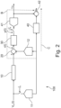
- FIG. 2 shows by dotted lines, that the transfer function of path C with the digital filter 40 is intended to be a replica of the transfer function of path B with the sampled analog path. If the two paths B, C are not matched, this is an indication that the output signal v is not zero and indicates that an optimized digital filter 40 is still not obtained.
- FIG. 3 shows modifications of the arrangement of FIG. 2 to find the filter coefficients of the digital filter 40, in order to perform a calibration procedure according to the proposed disclosure.
- the continuous-time filter 30 is implemented as a second order loop filter G(s). Now it is intended to find the filter coefficients FW of the digital filter 40 as accurate and as fast as possible. This is done via a so called “foreground calibration" which means, that during calibration the normal operation mode of the CTP ADC circuit 100 is not active or stopped, respectively.
- the signal calib is inactive and the signal calib is active and vice versa.
- the CTP ADC circuit 100 returns back to normal operation mode. In the normal operation mode, the signal calib closes the corresponding switch and the signal calib opens the corresponding switch.
- Initial value of the digital filter 40 (e.g. implemented aa an adaptive FIR filter) are all set to zero (can be set to nominal value also).
- the input 1 is disconnected and analog-delay path is connected to common-mode or zero.
- Gain stages 43, 44 can be implemented as a multiplier and are also bypassed in the calibration mode.
- the gain of the ADC1-DAC1 path is reduced to not saturate the continuous-time loop filter 30. This is done by either setting the "Gain" of analog-filter & digital-filter path to 1 or some low value.
- a signal (e.g. pseudo random source signal, even sine or another signal) of a signal source 60 is applied as an input of the sub DAC 12. There is no strict requirements as regards the type of the signal source 60.
- the signal delay t d of the delay element 10 should be matched to the ADC-DAC path delay to minimize the residue r(t).
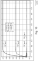
- FIG. 4 shows a convergence of the filter weights FW (FIR taps) with clock cycles.
- filter weights FW converge well within 20k cycles.
- the digital filter 40 may be an infinite impulse response filter (IIR filter), however, its impulse response dies down after few samples.
- IIR filter infinite impulse response filter
- the digital filter 40 can be approximated by an FIR-filter (finite impulse response filter). It is intended to implement a digital filter 40, whose response matches with the response of the continuous-time analog filter 30.
- the second columns shows the expected values of the filter coefficients and the third columns shows that values are close to the expected values in the second column and have been obtained after convergence.
- a value of the sampling rate f s of the output of the continuous-time filter 30 is equal to a value of the sampling rate f s of the sub DACs 11, 12.
- the value of the sampling rate f s of the output of the continuous-time filter 30 can also be smaller than a value of the sampling rate of the sub DACs 11, 12.
- the diagram of FIG. 4 shows filter coefficients FIR Tap 0 to FIR Tap 9, after 40k cycles all values of the coefficients have converged within a specified tolerance.
- the number of cycles is a predefined value which is known in advance. To take care of variations in process, temperature and to have an extra margin, the number of cycles may be somewhat over-dimensioned.
- the job of the algorithm e.g. LMS algorithm
- LMS algorithm is only exemplary, there are a lot of alternative algorithms which could be used.
- Requirement for LMS to converge is the provision of a pseudo random signal. It takes an amount of time to cancel the known signal and converge to the error err.
- the calibration device 50 takes the error signal err and the input signal s in of the signal source 60 and calculates the filter weights FW, which become the coefficients of the digital filter 40. Normalized LMS-algorithm is considered to be a very efficient algorithm in this context.
- FIG. 5 shows an output spectrum of the CTP ADC circuit 100 after the coefficients of the digital filter 40 have been calibrated as having been described above and the CTP ADC circuit 100 running in the normal operation mode.
- the spectrum is a result of an input signal to the CTP ADC circuit 100 with appr. 250 MHz with a sampling frequency fs of 1 GHz.
- fs sampling frequency
- the filter weights are updated after LMS convergence, the ADC performance is restored.
- FIG. 6 shows an output spectrum with the same filter coefficients, if the filter parameter w1 changes by 20%, e.g. due to RC-variation.
- the filter parameter w1 changes by 20%, e.g. due to RC-variation.
- the CTP ADC circuit 100 is hardly functional, because in terms of ADC performance the CTP ADC circuit 100 is degraded with the spectrum shown in FIG 6 .
- FIG. 7 shows a generalization of the proposed CTP ADC circuit 100 with two stages and the back end ADC 41.
- a first digital filter 40a (of the first stage) and a second digital filter 40b (of the second stage) are summed up via the second summation node 42, which provides the final output signal v.
- the calibration of both stages can be done in sequential or in parallel manner, though there is no significant difference between number of convergence cycles.
- the corresponding calibration signals are calib1, calib 1 (for the calibration of the first stage) and calib 2, calib 2 (for the calibration second stage), which are used as described above with respect to the single stage CTP ADC circuit 100 of FIG. 3 .
- the order of the calibration of the stages is arbitrary.
- the calibration of the two stages of the CTP ADC circuit 100 can be performed in the following three ways:
- filter coefficients of digital filters of CTP ADC circuits 100 with more than two stages can be calibrated in the above described manner.
- FIG. 9 shows a convergence of the second stage of the CTP ADC circuit 100 with FIR filter coefficients similar as shown in FIG. 4 .
- a calibration of is well done with 10k clock cycles.
- FIG. 10 shows a convergence of the first stage of the CTP ADC circuit 100 with FIR filter coefficients similar as shown in FIG. 9 .
- a calibration of is well done with 10k clock cycles.
- FIG. 11 shows a spectrum of the CTP ADC circuit after having calibrated the filter coefficients of both stages.
- a "DC-blocker" may be added in a so called “error-path” functionally coupled between the second summation node 42 and the calibration device 50 to the LMS loop which may block DC (hence remove offset) from digital error data.
- the DC-blocker can be implemented by minimum possible stages of IIR-, CIC-, or FIR-filter. Any other possible structures can be used to filter out DC component from the digital error data.
- Possible sources or offsets are e.g. the first summation nodes 20a, 20b. Any gain-mismatch after the first stage is naturally taken care as loop which will tried to be corrected as well.
- FIG. 12 shows three signal diagrams of the CTP ADC circuit 100 without said DC blocker.
- FIG. 12a shows a signal at the output of the second summation node 42
- FIG. 12b shows an ADC spectrum of a CTP ADC circuit 100 without DC blocker
- FIG. 12c shows a DNCF (digital noise cancellation filter, i.e. a digital filter which is tuned by the LMS-algorithm), with a settling of coefficients of a CTP ADC circuit 100 without DC blocker.
- DNCF digital noise cancellation filter
- FIG. 13 shows three signal diagrams of the CTP ADC circuit 100 having a DC blocker as mentioned above.
- FIG. 13a shows a DNCF settling of coefficients of a CTP ADC circuit 100 with DC blocker
- FIG. 13b shows input and output signals of said DC blocker
- FIG. 13c shows an ADC spectrum of a CTP ADC circuit 100 having a DC blocker.
- the DC blocker is also a digital filter which will block DC components form the digital input and its output is also digital without DC value.
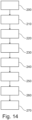
- FIG. 14 shows a principal flow of the proposed method.
- a step 200 the continuous-time analog-to-digital converter circuit (100) is set into a calibration mode.
- a calibration input signal is applied to an input 1.
- a step 220 the calibration input signal is delayed by means of a delay element 10 with a specified time delay t d , the delay element 10 functionally connected between the input 1 and a first summation node 20.
- a step 230 the calibration input signal is digitized and the digitized signal is reconverted to analog domain and to subtract it at the first summation node 20.
- a step 240 an output of the first summation node 20 is filtered by means of a continuous-time filter 30 and clocking the output of the continuous-time filter 30 with a specified sampling rate fs.
- a step 250 the clocked output of the continuous-time filter 30 is digitized by means of a backend ADC 41 and applied to a second summation node 42.
- an output signal v of the continuous-time analog-to-digital converter circuit 100 is provided by summing up the output of the backend ADC 41 with an output of a digital filter 40 being connected to a sub ADC being connected to the input 1.
- a replica of a transfer function of the sampled output of the continuous-time filter 30 is provided in the digital domain by means of the digital filter 40.
- the proposed CTP ADC circuit can be used for applications requiring high speed ADC.
- the proposed architecture also has anti-aliasing properties, which can help remove anti-aliasing filter or greatly relax its design.
- the proposed scheme can be implemented on-chip for foreground calibration. Signal required to feed input for DNCF estimation can be easily implemented as "digital waveform generator”.
- the proposed method implements a so called "foreground calibration" only which doesn't need very specific type of test-signal of the signal source 60. It can be multi-tone sine-wave, ramp-wave, chirp or even random input. As per our calibration, it's not necessary to feed digital test signal, even analog signal at the ADC input can be fed during calibration.
- the proposed method is to find the DNCF in a adaptive filter manner which starts from the most inner-loop (last stage) and sequentially finding all stage filters. All the stage filters can also be tuned simultaneously using LMS/NLMS but it seem to take bit longer time than sequential estimation. Our proposal also requires bit of change in the filter-dc-gain (set to 1) during calibration.
- circuits or circuitry which may be illustrated as or using terms such as blocks, modules, device, system, unit, controller, etc. and/or other circuit-type depictions.
- Such circuits or circuitry are used together with other elements to exemplify how certain embodiments may be carried out in the form or structures, steps, functions, operations, activities, etc.
- the logic circuitry may correspond to logic circuitry (which may refer to or include a code-programmed/configured CPU
- the logic circuitry may carry out a process or method (sometimes "algorithm") by performing such activities and/or steps associated with the above-discussed functionalities.
- the logic circuitry may carry out a process or method by performing these same activities/operations.
- one or more modules are discrete logic circuits or programmable logic circuits configured and arranged for implementing these operations/activities.
- a programmable circuit is one or more computer circuits, including memory circuitry for storing and accessing a program to be executed as a set (or sets) of instructions (and/or to be used as configuration data to define how the programmable circuit is to perform), and an algorithm or process as described above is used by the programmable circuit to perform the related steps, functions, operations, activities, etc.
- the instructions can be configured for implementation in logic circuitry, with the instructions (whether characterized in the form of object code, firmware or software) stored in and accessible from a memory (circuit).
- the instructions whether characterized in the form of object code, firmware or software
- a memory circuit
- the adjectives "first” and “second” are not used to connote any description of the structure or to provide any substantive meaning; rather, such adjectives are merely used for English-language antecedence to differentiate one such similarly-named structure from another similarly-named structure.
- the discloses devices, apparatuses, units, elements, systems and methods described herein may at least partially be embodied by a computer program or a plurality of computer programs, which may exist in a variety of forms both active and inactive in a single computer system or across multiple computer systems.
- they may exist as software program(s) comprised of program instructions in source code, object code, executable code or other formats for performing some of the steps.
- Any of the above may be embodied on a computer readable medium, which may include storage devices and signals, in compressed or uncompressed form.
Landscapes
- Engineering & Computer Science (AREA)
- Theoretical Computer Science (AREA)
- Physics & Mathematics (AREA)
- Nonlinear Science (AREA)
- Analogue/Digital Conversion (AREA)
Abstract
A continuous-time analog-to-digital converter circuit (100), comprising:
- an input (1) configured to receive an analog input signal (vin);
- a delay element (10) with a specified time delay (td), the delay element (10) functionally connected between the input (1) and a first summation node (20);
- a ADC-DAC path with a sub ADC (11) and a sub DAC (12) connected between the input (1) and the first summation node (20), the ADC-DAC path configured to digitize the analog input signal (vin) and to reconvert the digitized signal to analog domain and to subtract it at the first summation node (20);
- wherein an output of the first summation node (20) is filtered by means of a continuous-time filter (30), wherein an output of the continuous-time filter (30) is clocked by a specified sampling rate (fs);
- wherein a backend ADC (41) is configured to digitize the clocked output of the analog filter (30) and to connect the clocked output to a second summation node (42);
- wherein an output (v) is obtained by a summation of the output of the backend ADC (41) and an output of a digital filter (40) being connected to the sub ADC (11), characterized in that the digital filter (40) is configured to represent a replica of a transfer function of the sampled output of the continuous-time filter (30) in the digital domain.
- an input (1) configured to receive an analog input signal (vin);
- a delay element (10) with a specified time delay (td), the delay element (10) functionally connected between the input (1) and a first summation node (20);
- a ADC-DAC path with a sub ADC (11) and a sub DAC (12) connected between the input (1) and the first summation node (20), the ADC-DAC path configured to digitize the analog input signal (vin) and to reconvert the digitized signal to analog domain and to subtract it at the first summation node (20);
- wherein an output of the first summation node (20) is filtered by means of a continuous-time filter (30), wherein an output of the continuous-time filter (30) is clocked by a specified sampling rate (fs);
- wherein a backend ADC (41) is configured to digitize the clocked output of the analog filter (30) and to connect the clocked output to a second summation node (42);
- wherein an output (v) is obtained by a summation of the output of the backend ADC (41) and an output of a digital filter (40) being connected to the sub ADC (11), characterized in that the digital filter (40) is configured to represent a replica of a transfer function of the sampled output of the continuous-time filter (30) in the digital domain.
Description
- The present disclosure relates to continuous-time pipeline ADC. Furthermore, the present disclosure relates to a method of calibrating a digital filter of a continuous-time pipeline ADC.
- In a continuous-time pipeline (CTP) ADC, the digital outputs of various stages are combined to give the final ADC output signal. This reconstruction requires estimating digital filters for various stages. This digital reconstruction needs to match a sampled analog system. The digital filter needs to match an analog path, wherein mismatch degrades the overall performance of the CTP ADC.
-
US 10,432,210 B1 -
US 11,563,442 B2 -
US 11,218,158 B1 - It is an object of the present invention to provide an improved CTP ADC circuit.
- According to a first aspect, the present disclosure proposes a continuous-time analog-to-digital converter circuit, comprising:
- an input configured to receive an analog input signal;
- a delay element with a specified time delay, the delay element functionally connected between the input and a first summation node;
- a ADC-DAC path with a sub ADC and a sub DAC connected between the input and the first summation node, the ADC-DAC path configured to digitize the analog input signal and to reconvert the digitized signal to analog domain and to subtract it at the first summation node;
- wherein an output of the first summation node is filtered by means of a continuous-time filter, wherein an output of the continuous-time filter is clocked by a specified sampling rate;
- wherein a backend ADC is configured to digitize the clocked output of the analog filter and to connect the clocked output to a second summation node;
- wherein an output is obtained by a summation of the output of the backend ADC and an output of a digital filter being connected to the sub ADC, characterized in that the digital filter is configured to represent a replica of a transfer function of the sampled output of the continuous-time filter in the digital domain.
- It is assumed, that a delay of an ADC-DAC path is already tuned/programmed by any other method, wherein the digital filter of the proposed CTP ADC circuit only matches the analog path. This advantageously allows to increase a gain of the analog filter block, resulting in an improved performance of the CTP ADC circuit.
- According to a further aspect, the present disclosure proposes a method for calibrating a digital filter of a continuous-time analog-to-digital converter circuit, comprising the steps:
- setting the continuous-time analog-to-digital converter circuit into a calibration mode;
- applying a calibration input signal at an input;
- delaying the calibration input signal by means of a delay element with a specified time delay, the delay element functionally connected between the input and a first summation node;
- digitizing the calibration input signal and reconverting the digitized signal to analog domain and to subtract it at the first summation node;
- filtering an output of the first summation node by means of a continuous-time filter and clocking the output of the continuous-time filter with a specified sampling rate;
- digitizing the clocked output of the continuous-time filter by means of a backend ADC and applying it to a second summation node;
- providing an output signal of the continuous-time analog-to-digital converter circuit by summing up the output of the backend ADC with an output of a digital filter being connected to a sub ADC being connected to the input; and
- providing a replica of a transfer function of the sampled output of the continuous-time filter in the digital domain by means of the digital filter.
- In one or more embodiments, filter coefficients of said digital filter are provided by a calibration device.
- In one or more embodiments, the CTP ADC circuit further comprises a signal source being configured to feed its signal to the calibration device, wherein the output is applied to the calibration device, wherein the calibration device is configured to update the filter coefficients of the digital filter.
- According to one or more embodiments, the signal source is configured to generate one of the following: pseudo random signal, sine wave signal. Advantageously, even more alternative kinds of signal sources are possible to be used.
- According to one or more embodiments, the digital filter is one of the following: adaptive IIR-filter, adaptive FIR filter.
- According to one or more embodiments, the CTP ADC circuit comprises switches which are configured to set the ATP ADC circuit into a calibration mode and into normal operation mode.
- According to one or more embodiments, the CTP ADC circuit further comprises a gain stage between the sub ADC and the digital filter and/or a gain stage between the first summation node and the continuous-time filter, wherein at least one of said gain stages is bypassed in the calibration mode.
- According to one or more embodiments, a calibration algorithm running on the calibration device is a normalized LMS algorithm. The normalized LMS provides a fast way of implementing the calibration procedure of the digital filter.
- According to one or more embodiments, a number of calibration cycles of the calibration algorithm is known in advance, wherein after having performed the calibration the filter coefficients have converged within a specified tolerance. The number of cycles can be determined in advance, e.g. by means of a simulation process (e.g. MATLAB).
- According to one or more embodiments, the signal source and the calibration device are on-chip or off-chip. An on-chip signal source is easy to implement. Furthermore, also the calibration device is preferably implemented on-chip in order to perform calibration when temperature varies.
- According to one or more embodiments, the CTP ADC circuit further comprises a DC blocker functionally coupled between an output of the second summation node and the calibration device. In this way, DC components can be filtered from digital error data, i.e. an offset may be removed or at least reduced.
- According to one or more embodiments, the CTP ADC circuit is one of the following: IIR-filter, CIC-filter, FIR-filter.
- According to one or more embodiments, a value of the sampling rate of the output of the continuous-time filter is equal or smaller than a value of the sampling rate of the sub DACs.
- The above discussion/summary is not intended to describe each embodiment or every implementation of the present disclosure. The drawings and detailed description that follow also exemplify various embodiments. The aspects defined above and further aspects of the present disclosure are apparent from the examples of embodiment to be described hereinafter with reference to the appended drawings, which are explained with reference to the examples of embodiment. However, needless to say, that the disclosure is not limited to the examples of embodiments.
- All illustrations in the drawings are schematical. It is noted that in different figures, similar or identical elements or features are provided with the same reference signs or with reference signs that are different from the corresponding reference signs only within the first digit. In order to avoid unnecessary repetitions, elements or features which have already been elucidated with respect to a previously described embodiment are not elucidated again at a later position of the description.
- Various example embodiments may be more completely understood in consideration of the following detailed description in connection with the accompanying drawings, in which:
- FIG. 1
- shows a conventional CTP ADC circuit;
- FIG. 2
- shows the conventional CTP ADC circuit of
FIG. 1 indicating a principle work mechanism of the present disclosure; - FIG. 3
- shows an embodiment of a proposed CTP ADC circuit;
- FIG. 4
- is a diagram showing an effect of a calibration procedure;
- FIG. 5
- is a diagram with signals of an CTP ADC circuit in normal operation mode after having been calibrated its digital filter;
- FIG. 6
- is a signal diagram showing a result of a bad or no calibration of the CTP ADC circuit;
- FIGs. 7, 8
- are diagrams of a double stage CTP ADC circuit according to the present disclosure;
- FIG. 9
- is a diagram with signals of an CTP ADC circuit in normal operation mode after having been calibrated its digital filter;
- FIG. 10
- is a diagram with signals of a CTP ADC circuit in normal operation mode after having been calibrated its digital filter;
- FIG. 11
- is a diagram with signals of an CTP ADC circuit in normal operation mode after having been calibrated;
- FIG. 12
- shows signal diagrams of a proposed CTP ADC circuit without DC blocker;
- FIG. 13
- shows signal diagrams of a proposed CTP ADC circuit with a 3rd order IIR elliptic DC blocker; and
- FIG. 14
- shows a flow of the proposed method.
- While various embodiments discussed herein are amenable to modifications and alternative forms, aspects thereof have been shown by way of example in the drawings and will be described in detail. It should be understood, however, that the intention is not to limit the disclosure to the particular embodiments described. On the contrary, the intention is to cover all modifications, equivalents, and alternatives falling within the scope of the disclosure including aspects defined in the claims. In addition, the term "example" as used throughout this application is only by way of illustration, and not limitation.
-
FIG. 1 shows a block diagram of a conventional single stage continuous timeline analog-to-digital converter circuit 100. One recognizes aninput 1, to which an analog input signal vin(t) can be applied. Ananalog delay element 10 is connected to theinput 1 having a specific time delay td and is further connected to afirst summation node 20. An ADC-DAC path is interconnected between theinput 1 and thefirst summation node 20 comprising aswitch S 1, being switched with a specific rate fs, a sub-ADC 11 being connected to the switch S1 and the sub-DAC 12 being connected to the sub-ADC 11 and to thefirst summation node 20. In this way, a digitization and reconversion of the digitized analog input signal vin(t) into analog is performed and the reconverted digital is subtracted at thefirst summation node 20. An output of thefirst summation node 20 is a residue r(t), which is fed to a first analog filter 30 (continuous time filter G(s)). An output of thefirst analog filter 30 is sampled by means of a switch S2 with the specific rate fs and is applied to abackend ADC 41, which is connected to asecond summation node 42. Furthermore, the output of the sub-ADC 11a is also filtered by means of adigital filter 40, whose output is connected to thesecond summation node 42. An output of thesecond summation node 42 represents a final signal v of theCTP ADC circuit 100. Marked with dotted lines is an arrangement A which represents the sampled analog path with thesub DAC 12, thefirst summation node 20 and the continuous-time filter 30, wherein said arrangement A has a specific discrete transfer function. - It is proposed to note that the two sub-paths are inherently subtracted at the output signal v. If a signal is injected at the input of the sub DAC 12 (with vin=0), then the output signal v = 0 (ignoring quantization noise of the back-end ADC 41), if the two paths match. This observation is used to apply Least Mean Square (LMS) to the "error" v and adaptively update the
digital filter 40 to match the desired response. - A principal working mechanism is shown in
FIG. 2 which shows by dotted lines, that the transfer function of path C with thedigital filter 40 is intended to be a replica of the transfer function of path B with the sampled analog path. If the two paths B, C are not matched, this is an indication that the output signal v is not zero and indicates that an optimizeddigital filter 40 is still not obtained. -
FIG. 3 shows modifications of the arrangement ofFIG. 2 to find the filter coefficients of thedigital filter 40, in order to perform a calibration procedure according to the proposed disclosure. One recognizes a one stage CTP ADC circuit with a 2.5-bit sub ADC 11 and a back-end ADC 41 with 12-bit, wherein a sampling rate fs is 1GHz. The continuous-time filter 30 is implemented as a second order loop filter G(s). Now it is intended to find the filter coefficients FW of thedigital filter 40 as accurate and as fast as possible. This is done via a so called "foreground calibration" which means, that during calibration the normal operation mode of theCTP ADC circuit 100 is not active or stopped, respectively. That means, during normal operation the signal calib is inactive and the signalcalib is active and vice versa. Once thedigital filter 40 is calibrated, theCTP ADC circuit 100 returns back to normal operation mode. In the normal operation mode, the signal calib closes the corresponding switch and the signalcalib opens the corresponding switch. - Initial value of the digital filter 40 (e.g. implemented aa an adaptive FIR filter) are all set to zero (can be set to nominal value also). The
input 1 is disconnected and analog-delay path is connected to common-mode or zero. Gain stages 43, 44 can be implemented as a multiplier and are also bypassed in the calibration mode. - In the calibration mode the following steps are done:
The gain of the ADC1-DAC1 path is reduced to not saturate the continuous-time loop filter 30. This is done by either setting the "Gain" of analog-filter & digital-filter path to 1 or some low value. - Changes in this DC-gain can be avoided by having DAC with bit large number of levels (with reduced step-size) than ADC and extra levels are used only during calibration mode. In this case amplitude of test-signal is reduced to ensure backend ADC doesn't saturate.
- A signal (e.g. pseudo random source signal, even sine or another signal) of a
signal source 60 is applied as an input of thesub DAC 12. There is no strict requirements as regards the type of thesignal source 60. A calibration device 50 (e.g. running an LMS algorithm) updates the filter weights FW based on the "error" of the output signal v. After the convergence of the filter weights FW, calibration can be stopped, and normal ADC conversion start (calib = 0). Thecalibration device 50 tries to minimize the error signal err, which corresponds to the output signal v of thesecond summation node 42. Once the error is zero, it is known that this is the condition that thedigital filter 40 is matched to the continuous-time analog filter 30. It is known in advance after how many cycles the filter coefficients have converged. - The signal delay td of the
delay element 10 should be matched to the ADC-DAC path delay to minimize the residue r(t). The better the delay matching, the smaller the residue r(t), which allows to keep larger gain in the continuous-time filter 30, which relaxes the back-end ADC requirement. -
FIG. 4 shows a convergence of the filter weights FW (FIR taps) with clock cycles. One recognizes, that filter weights FW converge well within 20k cycles. Ideal filter weights for Zero Order Hold (ZOH) DAC can be expressed as follows:
- Based on the analog continuous-
time filter 30, whose transfer function is given in the denominator of the above formula, we achieve certain FIR filter coefficients as shown in the second part of the formula. - The
digital filter 40 may be an infinite impulse response filter (IIR filter), however, its impulse response dies down after few samples. For ease of implementation, thedigital filter 40 can be approximated by an FIR-filter (finite impulse response filter). It is intended to implement adigital filter 40, whose response matches with the response of the continuous-time analog filter 30. - The following table shows a comparison of exemplary ideal filter weights FW vs. obtained filter weights FW after LMS-convergence:
Table 1 Filter tap Ideal coefficient Coefficient after LMS convergence 0 0 0 1 0.785508 0.785468 2 0.257663 0.257684 3 -0.033318 -0.033310 4 -0.011714 -0.011707 5 0.001488 0.001488 - The second columns shows the expected values of the filter coefficients and the third columns shows that values are close to the expected values in the second column and have been obtained after convergence.
- A value of the sampling rate fs of the output of the continuous-
time filter 30 is equal to a value of the sampling rate fs of thesub DACs time filter 30 can also be smaller than a value of the sampling rate of thesub DACs backend ADC 41 can be same or smaller than the sampling rate of thesub DACs - The diagram of
FIG. 4 shows filtercoefficients FIR Tap 0 toFIR Tap 9, after 40k cycles all values of the coefficients have converged within a specified tolerance. One recognizes, that after 40k cycles the signalcalib goes HIGH, which means that the calibration procedure of the CTP ADC circuit has stopped. The number of cycles is a predefined value which is known in advance. To take care of variations in process, temperature and to have an extra margin, the number of cycles may be somewhat over-dimensioned. The job of the algorithm (e.g. LMS algorithm) changes all the parameters simultaneously and tries to move all the parameters in a direction, which would converge to the right value. LMS algorithm is only exemplary, there are a lot of alternative algorithms which could be used. Requirement for LMS to converge is the provision of a pseudo random signal. It takes an amount of time to cancel the known signal and converge to the error err. Thecalibration device 50 takes the error signal err and the input signal sin of thesignal source 60 and calculates the filter weights FW, which become the coefficients of thedigital filter 40. Normalized LMS-algorithm is considered to be a very efficient algorithm in this context. -
FIG. 5 shows an output spectrum of theCTP ADC circuit 100 after the coefficients of thedigital filter 40 have been calibrated as having been described above and theCTP ADC circuit 100 running in the normal operation mode. The spectrum is a result of an input signal to theCTP ADC circuit 100 with appr. 250 MHz with a sampling frequency fs of 1 GHz. One recognizes, that the coefficients of thedigital filter 40 are working as expected. - If the calibration is enabled, the filter weights are updated after LMS convergence, the ADC performance is restored.
-
FIG. 6 shows an output spectrum with the same filter coefficients, if the filter parameter w1 changes by 20%, e.g. due to RC-variation. One recognizes again the maximum of the input signal of appr. 250 MHz having been applied to theCTP ADC circuit 100, however, with much more spectral noise than in the spectrum shown inFIG. 5 . In result, theCTP ADC circuit 100 is hardly functional, because in terms of ADC performance theCTP ADC circuit 100 is degraded with the spectrum shown inFIG 6 . -
FIG. 7 shows a generalization of the proposedCTP ADC circuit 100 with two stages and theback end ADC 41. In order to get the final output signal v, output signals of theback end ADC 41, a firstdigital filter 40a (of the first stage) and a seconddigital filter 40b (of the second stage) are summed up via thesecond summation node 42, which provides the final output signal v. The calibration of both stages can be done in sequential or in parallel manner, though there is no significant difference between number of convergence cycles. - The corresponding calibration signals are calib1,
calib1 (for the calibration of the first stage) andcalib 2,calib2 (for the calibration second stage), which are used as described above with respect to the single stageCTP ADC circuit 100 ofFIG. 3 . The order of the calibration of the stages is arbitrary. - A sequential method is described in the following. The second stage is calibrated by making the signal calib2 = 1. Once the filter coefficients of the second
digital filter 40b converge, calibration is stopped. Gain of the second stage is by-passed to prevent loop saturation. - Afterwards, the first stage is calibrated by making the signals calibi =1 and calib2 = 0. As before, gain stage is by-passed. Once the filter coefficients of the first
digital filter 40a converge, calibration is stopped, and normal ADC conversion of theCTP ADC circuit 100 can start. - Referring to
FIG. 7 now, the calibration of the two stages of theCTP ADC circuit 100 can be performed in the following three ways: - (i) Configuration 1: Sequential
- Step 1: calibi=0, calib2=1 and calib3=1 (finds filter coefficients of the second stage), then
- Step 2 : calib1=1, calib2=1 and calib3=0 (finds filter coefficients of the first stage),
- Step 3 : calibi=0, calib2=0 and calib3=0 normal operation, after calibration
- (ii) Configuration 2: Sequential
- Step 1 : calib1=1, calib2=1 and calib3=0 (finds filter coefficients of the first stage), then
- Step2 : calibi=0, calib2=1 and calib3=1 (finds filter coefficients of the second stage)
- Step3 : calibi=0, calib2=0 and calib3=0 normal operation, after calibration
- (iii) Configuration 3: Parallel
- calib1=1, calib2=0 and calib3=0 (finds filter coefficients of both stages simultaneously)
- calibi=0, calib2=0 and calib3=0 after calibration
- In parallel mode, both calib2 and calib3 switches can be removed as they are always off
FIG. 8 shows an arrangement of aCTP ADC circuit 100 for which a slight variant of the parallel configuration is performed. One recognizes, that in this case some switches of the second stage are not required, because they are always on or always off: - (iv) Configuration 3: Parallel modified
- calibi=1 (finds filter coefficients of both stages simultaneously)
- calibi=0 after calibration.
- Of course, also filter coefficients of digital filters of
CTP ADC circuits 100 with more than two stages (not shown) can be calibrated in the above described manner. -
FIG. 9 shows a convergence of the second stage of theCTP ADC circuit 100 with FIR filter coefficients similar as shown inFIG. 4 . One recognizes, that a calibration of is well done with 10k clock cycles. -
FIG. 10 shows a convergence of the first stage of theCTP ADC circuit 100 with FIR filter coefficients similar as shown inFIG. 9 . One recognizes, that a calibration of is well done with 10k clock cycles. -
FIG. 11 shows a spectrum of the CTP ADC circuit after having calibrated the filter coefficients of both stages. One recognizes 90.1 dB (2-bits from the first stage, 1-bit from the second stage, 12-bits from back-end ADC 41). - In further alternative embodiments of the proposed CTP ADC circuit 100 a "DC-blocker" (not shown) may be added in a so called "error-path" functionally coupled between the
second summation node 42 and thecalibration device 50 to the LMS loop which may block DC (hence remove offset) from digital error data. The DC-blocker can be implemented by minimum possible stages of IIR-, CIC-, or FIR-filter. Any other possible structures can be used to filter out DC component from the digital error data. - Possible sources or offsets are e.g. the
first summation nodes - To include a gain-mismatch error of the first stage, gain-bypass can be removed (calib1= 0) and multi-level sub-DAC can be used with reduced amplitude of a test signal (ideally "Full-scale/Gain"). More number of sub DAC levels supports that a small test signal is still bit larger than a step-size of the sub DAC.
-
FIG. 12 shows three signal diagrams of theCTP ADC circuit 100 without said DC blocker. -
FIG. 12a shows a signal at the output of thesecond summation node 42,FIG. 12b shows an ADC spectrum of aCTP ADC circuit 100 without DC blocker andFIG. 12c shows a DNCF (digital noise cancellation filter, i.e. a digital filter which is tuned by the LMS-algorithm), with a settling of coefficients of aCTP ADC circuit 100 without DC blocker. -
FIG. 13 shows three signal diagrams of theCTP ADC circuit 100 having a DC blocker as mentioned above. -
FIG. 13a shows a DNCF settling of coefficients of aCTP ADC circuit 100 with DC blocker,FIG. 13b shows input and output signals of said DC blocker andFIG. 13c shows an ADC spectrum of aCTP ADC circuit 100 having a DC blocker. The DC blocker is also a digital filter which will block DC components form the digital input and its output is also digital without DC value. -
FIG. 14 shows a principal flow of the proposed method. - In a
step 200 the continuous-time analog-to-digital converter circuit (100) is set into a calibration mode. - In a step 210 a calibration input signal is applied to an
input 1. - In a
step 220 the calibration input signal is delayed by means of adelay element 10 with a specified time delay td, thedelay element 10 functionally connected between theinput 1 and afirst summation node 20. - In a
step 230 the calibration input signal is digitized and the digitized signal is reconverted to analog domain and to subtract it at thefirst summation node 20. - In a
step 240 an output of thefirst summation node 20 is filtered by means of a continuous-time filter 30 and clocking the output of the continuous-time filter 30 with a specified sampling rate fs. - In a
step 250 the clocked output of the continuous-time filter 30 is digitized by means of abackend ADC 41 and applied to asecond summation node 42. - In a
step 260 an output signal v of the continuous-time analog-to-digital converter circuit 100 is provided by summing up the output of thebackend ADC 41 with an output of adigital filter 40 being connected to a sub ADC being connected to theinput 1. - In a step 270 a replica of a transfer function of the sampled output of the continuous-
time filter 30 is provided in the digital domain by means of thedigital filter 40. - The proposed CTP ADC circuit can be used for applications requiring high speed ADC. The proposed architecture also has anti-aliasing properties, which can help remove anti-aliasing filter or greatly relax its design. The proposed scheme can be implemented on-chip for foreground calibration. Signal required to feed input for DNCF estimation can be easily implemented as "digital waveform generator".
- The proposed method implements a so called "foreground calibration" only which doesn't need very specific type of test-signal of the
signal source 60. It can be multi-tone sine-wave, ramp-wave, chirp or even random input. As per our calibration, it's not necessary to feed digital test signal, even analog signal at the ADC input can be fed during calibration. - The proposed method is to find the DNCF in a adaptive filter manner which starts from the most inner-loop (last stage) and sequentially finding all stage filters. All the stage filters can also be tuned simultaneously using LMS/NLMS but it seem to take bit longer time than sequential estimation. Our proposal also requires bit of change in the filter-dc-gain (set to 1) during calibration.
- In the foregoing description various specific details have been set forth to describe specific examples presented herein. It should be apparent to one skilled in the art, however, that one or more other examples and/or variations of these examples may be practiced without all the specific details given below. In other instances, well known features have not been described in detail so as not to obscure the description of the examples herein. For ease of illustration, the same reference signs may be used in different diagrams to refer to the same elements or additional instances of the same element. Also, although aspects and features may in some cases be described in individual figures, it will be appreciated that features from one figure or embodiment can be combined with features of another figure or embodiment even though the combination is not explicitly shown or explicitly described as a combination.
- As examples, the specification describes and/or illustrates aspects useful for implementing the claimed disclosure by way of various circuits or circuitry which may be illustrated as or using terms such as blocks, modules, device, system, unit, controller, etc. and/or other circuit-type depictions. Such circuits or circuitry are used together with other elements to exemplify how certain embodiments may be carried out in the form or structures, steps, functions, operations, activities, etc. As examples, wherein such circuits or circuitry may correspond to logic circuitry (which may refer to or include a code-programmed/configured CPU, in one example the logic circuitry may carry out a process or method (sometimes "algorithm") by performing such activities and/or steps associated with the above-discussed functionalities. In other examples, the logic circuitry may carry out a process or method by performing these same activities/operations.
- For example, in certain of the above-discussed embodiments, one or more modules are discrete logic circuits or programmable logic circuits configured and arranged for implementing these operations/activities. In certain embodiments, such a programmable circuit is one or more computer circuits, including memory circuitry for storing and accessing a program to be executed as a set (or sets) of instructions (and/or to be used as configuration data to define how the programmable circuit is to perform), and an algorithm or process as described above is used by the programmable circuit to perform the related steps, functions, operations, activities, etc. Depending on the application, the instructions (and/or configuration data) can be configured for implementation in logic circuitry, with the instructions (whether characterized in the form of object code, firmware or software) stored in and accessible from a memory (circuit). As another example, where the specification may make reference to a "first" type of structure, a "second" type of structure, where the adjectives "first" and "second" are not used to connote any description of the structure or to provide any substantive meaning; rather, such adjectives are merely used for English-language antecedence to differentiate one such similarly-named structure from another similarly-named structure.
- Based upon the above discussion and illustrations, those skilled in the art will readily recognize, that various modifications and changes may be made to the various embodiments without strictly following the exemplary embodiments and applications illustrated and described herein. For example, methods as exemplified in the Figures may involve steps carried out in various orders, with one or more aspects of the embodiments herein retained, or may involve fewer or more steps.
- It should be noted that the term "comprising" does not exclude other elements or steps and "a" or "an" does not exclude a plurality. Also elements described in association with different embodiments may be combined. It should also be noted, that reference signs in the claims should not be construed as limiting the scope of the claims.
- The discloses devices, apparatuses, units, elements, systems and methods described herein may at least partially be embodied by a computer program or a plurality of computer programs, which may exist in a variety of forms both active and inactive in a single computer system or across multiple computer systems. For example, they may exist as software program(s) comprised of program instructions in source code, object code, executable code or other formats for performing some of the steps. Any of the above may be embodied on a computer readable medium, which may include storage devices and signals, in compressed or uncompressed form.
- It is noted that the embodiments above have been described with reference to different subject-matters. In particular, some embodiments may have been described with reference to method-type claims whereas other embodiments may have been described with reference to apparatus-type claims.
- However, a person skilled in the art will gather from the above that, unless otherwise indicated, in addition to any combination of features belonging to one type of subject-matter also any combination of features relating to different subject-matters, in particular a combination of features of the method-type claims and features of the apparatus-type claims, is considered to be disclosed with this document.
- It has to be noted that embodiments have been described with reference to different subject matters. In particular, some embodiments have been described with reference to method type claims whereas other embodiments have been described with reference to apparatus type claims.
- However, a person skilled in the art will gather from the above and the following description that, unless other notified, in addition to any combination of features belonging to one type of subject matter also any combination between features relating to different subject matters, in particular between features of the method type claims and features of the apparatus type claims is considered as to be disclosed with this application.
-
- 1
- input
- 10, 10a, 10b
- delay element
- 11, 11a, 11b
- sub ADC
- 12, 12a, 12b
- sub DAC
- 20, 20a, 20b
- 1st summation node
- 30, 30a, 30b
- continuous-time filter
- 40, 40a, 40b
- digital filter
- 41
- backend ADC
- 42
- 2nd summation node
- 43
- DC gain stage
- 44
- DC gain stage
- 50
- calibration device
- 60
- signal source
- 100
- CTP ADC device
- 200... 270
- method steps
- err
- error signal
- FW
- filter weights
Claims (15)
- A continuous-time analog-to-digital converter circuit (100), comprising:- an input (1) configured to receive an analog input signal (vin);- a delay element (10) with a specified time delay (td), the delay element (10) functionally connected between the input (1) and a first summation node (20);- a ADC-DAC path with a sub ADC (11) and a sub DAC (12) connected between the input (1) and the first summation node (20), the ADC-DAC path configured to digitize the analog input signal (vin) and to reconvert the digitized signal to analog domain and to subtract it at the first summation node (20);- wherein an output of the first summation node (20) is filtered by means of a continuous-time filter (30), wherein an output y(t) of the continuous-time filter (30) is clocked by a specified sampling rate (fs);- wherein a backend ADC (41) is configured to digitize the clocked output y(t) of the analog filter (30) and to connect the clocked output to a second summation node (42);- wherein an output (v) is obtained by a summation of the output of the backend ADC (41) and an output of a digital filter (40) being connected to the sub ADC (11), characterized in that the digital filter (40) is configured to represent a replica of a transfer function of the sampled output y(t) of the continuous-time filter (30) in the digital domain.
- Continuous-time analog-to-digital converter circuit (100) according to claim 1, wherein filter coefficients of said digital filter (40) are provided by a calibration device (50).
- Continuous-time analog-to-digital converter circuit (100) according to claim 2, further comprising a signal source (60), being configured to feed its signal (sin) to the calibration device (50), wherein the output (v) is applied to the calibration device (50), wherein the calibration device is configured to update the filter coefficients (FW) of the digital filter (40).
- Continuous-time analog-to-digital converter circuit (100) according to claim 3, wherein the signal source (60) is configured to generate one of the following: pseudo random signal, sine wave signal.
- Continuous-time analog-to-digital converter circuit (100) according to any of the preceding claims, wherein the digital filter (40) is one of the following: adaptive IIR-filter, adaptive FIR filter.
- Continuous-time analog-to-digital converter circuit (100) according to any of the preceding claims, comprising switches which are configured to set the ATP ADC circuit (100) into a calibration mode and into normal operation mode.
- Continuous-time analog-to-digital converter circuit (100) according to claim 6, further comprising a gain stage (43) between the sub ADC (11) and the digital filter (40) and/or a gain stage (44) between the first summation node (20) and the continuous-time filter (30), wherein at least one of said gain stages (43, 44) is bypassed in the calibration mode.
- Continuous-time analog-to-digital converter circuit (100) according to any of the preceding claims, wherein a calibration algorithm running on the calibration device (50) is a normalized LMS algorithm.
- Continuous-time analog-to-digital converter circuit (100) according to claim 8, wherein a number of calibration cycles of the calibration algorithm is known in advance, wherein after having performed the calibration the filter coefficients have converged within a specified tolerance.
- Continuous-time analog-to-digital converter circuit (100) according to any of the preceding claims, further comprising a DC blocker functionally coupled between an output of the second summation node (42) and the calibration device (50).
- Continuous-time analog-to-digital converter circuit (100) according to claim 10, wherein the DC blocker is one of the following: IIR-filter, CIC-filter, FIR-filter.
- Continuous-time analog-to-digital converter circuit (100) according to any of the preceding claims, wherein a value of the sampling rate (fs) of the output y(t) of the continuous-time filter (30) is equal or smaller than a value of the sampling rate (fs) of the sub DACs (11, 12).
- Method for calibrating a digital filter (42) of a continuous-time analog-to-digital converter circuit (100), comprising the steps:- setting the continuous-time analog-to-digital converter circuit (100) into a calibration mode;- applying a calibration input signal at an input (1);- delaying the calibration input signal by means of a delay element (10) with a specified time delay (td), the delay element (10) functionally connected between the input (1) and a first summation node (20);- digitizing the calibration input signal (vin) and reconverting the digitized signal to analog domain and to subtract it at the first summation node (20);- filtering an output of the first summation node (20) by means of a continuous-time filter (30) and clocking the output of the continuous-time filter (30) with a specified sampling rate (fs);- digitizing the clocked output of the continuous-time filter (30) by means of a backend ADC (41) and applying it to a second summation node (42);- providing an output signal (v) of the continuous-time analog-to-digital converter circuit (100) by summing up the output of the backend ADC (41) with an output of a digital filter (40) being connected to a sub ADC (11) being connected to the input (1); and- providing a replica of a transfer function of the sampled output of the continuous-time filter (30) in the digital domain by means of the digital filter (40).
- Method according to claim 12, wherein by means of the calibration device (50) an RMS error of the output signal (v) is minimized.
- Method according to claim 13 or 14, wherein a number of cycles of a calibration procedure is performed, wherein the number of cycles cause the coefficients of the digital filter (40) to converge within a specified tolerance band.
Applications Claiming Priority (1)
| Application Number | Priority Date | Filing Date | Title |
|---|---|---|---|
| IN202341083007 | 2023-12-06 |
Publications (1)
| Publication Number | Publication Date |
|---|---|
| EP4568112A1 true EP4568112A1 (en) | 2025-06-11 |
Family
ID=89941071
Family Applications (1)
| Application Number | Title | Priority Date | Filing Date |
|---|---|---|---|
| EP24157514.1A Pending EP4568112A1 (en) | 2023-12-06 | 2024-02-14 | Continuous-time pipeline adc and method for calibrating a digital filter of a continuous-time pipeline adc |
Country Status (3)
| Country | Link |
|---|---|
| US (1) | US20250192792A1 (en) |
| EP (1) | EP4568112A1 (en) |
| CN (1) | CN120110396A (en) |
Families Citing this family (1)
| Publication number | Priority date | Publication date | Assignee | Title |
|---|---|---|---|---|
| US10931299B1 (en) * | 2020-03-31 | 2021-02-23 | Taiwan Semiconductor Manufacturing Company, Ltd. | Analog to digital converter with VCO-based and pipelined quantizers |
Citations (4)
| Publication number | Priority date | Publication date | Assignee | Title |
|---|---|---|---|---|
| US10432210B1 (en) | 2018-07-05 | 2019-10-01 | Analog Devices Global Unlimited Company | Oversampled continuous-time pipeline ADC with digital signal reconstruction |
| US11218158B1 (en) | 2021-01-21 | 2022-01-04 | Analog Devices International Unlimited Company | Digital estimation of transfer functions in continuous-time analog-to-digital converters |
| CN114928349A (en) * | 2022-06-27 | 2022-08-19 | 奉加微电子(昆山)有限公司 | Continuous time pipeline analog-to-digital converter and digital reconstruction filter thereof |
| US11563442B2 (en) | 2020-08-07 | 2023-01-24 | Analog Devices International Unlimited Company | Calibration of continuous-time residue generation systems for analog-to-digital converters |
Family Cites Families (2)
| Publication number | Priority date | Publication date | Assignee | Title |
|---|---|---|---|---|
| US9614510B2 (en) * | 2015-03-13 | 2017-04-04 | Texas Instruments Incorporated | Input path matching in pipelined continuous-time analog-to-digital converters |
| US11652491B2 (en) * | 2020-08-07 | 2023-05-16 | Analog Devices International Unlimited Company | High-pass shaped dither in continuous-time residue generation systems for analog-to-digital converters |
-
2024
- 2024-02-14 EP EP24157514.1A patent/EP4568112A1/en active Pending
- 2024-11-14 CN CN202411625666.6A patent/CN120110396A/en active Pending
- 2024-12-05 US US18/970,141 patent/US20250192792A1/en active Pending
Patent Citations (4)
| Publication number | Priority date | Publication date | Assignee | Title |
|---|---|---|---|---|
| US10432210B1 (en) | 2018-07-05 | 2019-10-01 | Analog Devices Global Unlimited Company | Oversampled continuous-time pipeline ADC with digital signal reconstruction |
| US11563442B2 (en) | 2020-08-07 | 2023-01-24 | Analog Devices International Unlimited Company | Calibration of continuous-time residue generation systems for analog-to-digital converters |
| US11218158B1 (en) | 2021-01-21 | 2022-01-04 | Analog Devices International Unlimited Company | Digital estimation of transfer functions in continuous-time analog-to-digital converters |
| CN114928349A (en) * | 2022-06-27 | 2022-08-19 | 奉加微电子(昆山)有限公司 | Continuous time pipeline analog-to-digital converter and digital reconstruction filter thereof |
Non-Patent Citations (1)
| Title |
|---|
| DONG LIRAN ET AL: "A 2-GS/s 200-MHz BW Oversampling Continuous-Time Pipeline ADC with Adaptive Digital Filter in 28nm", 2021 IEEE INTERNATIONAL CONFERENCE ON INTEGRATED CIRCUITS, TECHNOLOGIES AND APPLICATIONS (ICTA), IEEE, 24 November 2021 (2021-11-24), pages 245 - 246, XP033996982, ISBN: 978-1-6654-1745-7, [retrieved on 20211222], DOI: 10.1109/ICTA53157.2021.9661855 * |
Also Published As
| Publication number | Publication date |
|---|---|
| US20250192792A1 (en) | 2025-06-12 |
| CN120110396A (en) | 2025-06-06 |
Similar Documents
| Publication | Publication Date | Title |
|---|---|---|
| US11329660B2 (en) | VCO-based continuous-time pipelined ADC | |
| US10651870B2 (en) | Input path matching in pipelined continuous-time analog-to-digital converters | |
| AU2005228155B2 (en) | Digital linearizing system | |
| US6177893B1 (en) | Parallel processing analog and digital converter | |
| US5257026A (en) | Method and apparatus for calibrating a multi-bit delta-sigma modular | |
| US6489913B1 (en) | Sub-ranging analog-to-digital converter using a sigma delta converter | |
| US10432210B1 (en) | Oversampled continuous-time pipeline ADC with digital signal reconstruction | |
| US11563442B2 (en) | Calibration of continuous-time residue generation systems for analog-to-digital converters | |
| US11652491B2 (en) | High-pass shaped dither in continuous-time residue generation systems for analog-to-digital converters | |
| JPH0793581B2 (en) | Sigma Delta analog / digital converter | |
| CN108494403B (en) | Double-channel TIADC sampling holding circuit mismatch self-adaptive calibration method | |
| KR20180130566A (en) | Digital Audio Converters & Amplifier Controllers | |
| US20250192792A1 (en) | Continuous-time pipeline adc and method for calibrating a digital filter of a continuous-time pipeline adc | |
| US9685975B2 (en) | Distributed combiner for parallel discrete-to-linear converters | |
| WO2018064720A1 (en) | A device, system and method for digital-to-analogue conversion | |
| CN119836751A (en) | Aliasing suppression in analog-to-digital converters (ADCs) | |
| Pavan et al. | Analysis of RC time-constant variations in continuous-time pipelined ADCs | |
| JP5286420B2 (en) | Analog-digital converter and semiconductor integrated circuit device using the same | |
| US6130633A (en) | Multibit digital to analog converter with feedback across the discrete time/continuous time interface | |
| Kong et al. | Subsampling mismatch noise cancellation for high-speed continuous-time DACs | |
| US6121909A (en) | One bit digital to analog converter with feedback across the discrete time/continuous time interface | |
| Khakpour et al. | Adaptive noise cancellation based architecture for correction of gain and offset mismatch errors in time-interleaved ADC | |
| JP3113525B2 (en) | A / D converter | |
| EP4568113A1 (en) | Continuous-time pipeline adc and method for a delay matching technique in a continuous-time pipeline adc | |
| O'Donoghue et al. | A Digitally Corrected 5-mW 2-MS/s SC $\Delta\Sigma $ ADC in 0.25-$\mu $ m CMOS With 94-dB SFDR |
Legal Events
| Date | Code | Title | Description |
|---|---|---|---|
| PUAI | Public reference made under article 153(3) epc to a published international application that has entered the european phase |
Free format text: ORIGINAL CODE: 0009012 |
|
| STAA | Information on the status of an ep patent application or granted ep patent |
Free format text: STATUS: THE APPLICATION HAS BEEN PUBLISHED |
|
| AK | Designated contracting states |
Kind code of ref document: A1 Designated state(s): AL AT BE BG CH CY CZ DE DK EE ES FI FR GB GR HR HU IE IS IT LI LT LU LV MC ME MK MT NL NO PL PT RO RS SE SI SK SM TR |
|
| STAA | Information on the status of an ep patent application or granted ep patent |
Free format text: STATUS: REQUEST FOR EXAMINATION WAS MADE |
|
| 17P | Request for examination filed |
Effective date: 20251211 |