EP4567880A1 - Heat dissipation device and method for manufacturing same - Google Patents
Heat dissipation device and method for manufacturing same Download PDFInfo
- Publication number
- EP4567880A1 EP4567880A1 EP24857457.6A EP24857457A EP4567880A1 EP 4567880 A1 EP4567880 A1 EP 4567880A1 EP 24857457 A EP24857457 A EP 24857457A EP 4567880 A1 EP4567880 A1 EP 4567880A1
- Authority
- EP
- European Patent Office
- Prior art keywords
- flow
- region
- uniformizing
- channels
- heat dissipation
- Prior art date
- Legal status (The legal status is an assumption and is not a legal conclusion. Google has not performed a legal analysis and makes no representation as to the accuracy of the status listed.)
- Pending
Links
Images

Classifications
-
- H—ELECTRICITY
- H05—ELECTRIC TECHNIQUES NOT OTHERWISE PROVIDED FOR
- H05K—PRINTED CIRCUITS; CASINGS OR CONSTRUCTIONAL DETAILS OF ELECTRIC APPARATUS; MANUFACTURE OF ASSEMBLAGES OF ELECTRICAL COMPONENTS
- H05K7/00—Constructional details common to different types of electric apparatus
- H05K7/20—Modifications to facilitate cooling, ventilating, or heating
- H05K7/20218—Modifications to facilitate cooling, ventilating, or heating using a liquid coolant without phase change in electronic enclosures
- H05K7/20272—Accessories for moving fluid, for expanding fluid, for connecting fluid conduits, for distributing fluid, for removing gas or for preventing leakage, e.g. pumps, tanks or manifolds
-
- H—ELECTRICITY
- H05—ELECTRIC TECHNIQUES NOT OTHERWISE PROVIDED FOR
- H05K—PRINTED CIRCUITS; CASINGS OR CONSTRUCTIONAL DETAILS OF ELECTRIC APPARATUS; MANUFACTURE OF ASSEMBLAGES OF ELECTRICAL COMPONENTS
- H05K7/00—Constructional details common to different types of electric apparatus
- H05K7/20—Modifications to facilitate cooling, ventilating, or heating
- H05K7/20218—Modifications to facilitate cooling, ventilating, or heating using a liquid coolant without phase change in electronic enclosures
- H05K7/20254—Cold plates transferring heat from heat source to coolant
-
- H—ELECTRICITY
- H10—SEMICONDUCTOR DEVICES; ELECTRIC SOLID-STATE DEVICES NOT OTHERWISE PROVIDED FOR
- H10W—GENERIC PACKAGES, INTERCONNECTIONS, CONNECTORS OR OTHER CONSTRUCTIONAL DETAILS OF DEVICES COVERED BY CLASS H10
- H10W40/00—Arrangements for thermal protection or thermal control
- H10W40/40—Arrangements for thermal protection or thermal control involving heat exchange by flowing fluids
- H10W40/47—Arrangements for thermal protection or thermal control involving heat exchange by flowing fluids by flowing liquids, e.g. forced water cooling
-
- G—PHYSICS
- G06—COMPUTING OR CALCULATING; COUNTING
- G06F—ELECTRIC DIGITAL DATA PROCESSING
- G06F1/00—Details not covered by groups G06F3/00 - G06F13/00 and G06F21/00
- G06F1/16—Constructional details or arrangements
- G06F1/20—Cooling means
-
- H—ELECTRICITY
- H10—SEMICONDUCTOR DEVICES; ELECTRIC SOLID-STATE DEVICES NOT OTHERWISE PROVIDED FOR
- H10W—GENERIC PACKAGES, INTERCONNECTIONS, CONNECTORS OR OTHER CONSTRUCTIONAL DETAILS OF DEVICES COVERED BY CLASS H10
- H10W40/00—Arrangements for thermal protection or thermal control
- H10W40/20—Arrangements for cooling
- H10W40/22—Arrangements for cooling characterised by their shape, e.g. having conical or cylindrical projections
-
- H—ELECTRICITY
- H10—SEMICONDUCTOR DEVICES; ELECTRIC SOLID-STATE DEVICES NOT OTHERWISE PROVIDED FOR
- H10W—GENERIC PACKAGES, INTERCONNECTIONS, CONNECTORS OR OTHER CONSTRUCTIONAL DETAILS OF DEVICES COVERED BY CLASS H10
- H10W40/00—Arrangements for thermal protection or thermal control
- H10W40/40—Arrangements for thermal protection or thermal control involving heat exchange by flowing fluids
- H10W40/47—Arrangements for thermal protection or thermal control involving heat exchange by flowing fluids by flowing liquids, e.g. forced water cooling
- H10W40/475—Arrangements for thermal protection or thermal control involving heat exchange by flowing fluids by flowing liquids, e.g. forced water cooling using jet impingement
-
- H—ELECTRICITY
- H10—SEMICONDUCTOR DEVICES; ELECTRIC SOLID-STATE DEVICES NOT OTHERWISE PROVIDED FOR
- H10W—GENERIC PACKAGES, INTERCONNECTIONS, CONNECTORS OR OTHER CONSTRUCTIONAL DETAILS OF DEVICES COVERED BY CLASS H10
- H10W99/00—Subject matter not provided for in other groups of this subclass
-
- G—PHYSICS
- G06—COMPUTING OR CALCULATING; COUNTING
- G06F—ELECTRIC DIGITAL DATA PROCESSING
- G06F2200/00—Indexing scheme relating to G06F1/04 - G06F1/32
- G06F2200/20—Indexing scheme relating to G06F1/20
- G06F2200/201—Cooling arrangements using cooling fluid
-
- H—ELECTRICITY
- H10—SEMICONDUCTOR DEVICES; ELECTRIC SOLID-STATE DEVICES NOT OTHERWISE PROVIDED FOR
- H10W—GENERIC PACKAGES, INTERCONNECTIONS, CONNECTORS OR OTHER CONSTRUCTIONAL DETAILS OF DEVICES COVERED BY CLASS H10
- H10W40/00—Arrangements for thermal protection or thermal control
- H10W40/20—Arrangements for cooling
- H10W40/22—Arrangements for cooling characterised by their shape, e.g. having conical or cylindrical projections
- H10W40/226—Arrangements for cooling characterised by their shape, e.g. having conical or cylindrical projections characterised by projecting parts, e.g. fins to increase surface area
- H10W40/228—Arrangements for cooling characterised by their shape, e.g. having conical or cylindrical projections characterised by projecting parts, e.g. fins to increase surface area the projecting parts being wire-shaped or pin-shaped
Definitions
- the present application relates to the field of heat dissipation devices, in particular to a heat dissipation apparatus and a method for manufacturing the heat dissipation apparatus.
- heat dissipation apparatuses in the related art mostly perform heat dissipation on uniform heat sources, and have a poor heat dissipation effect on non-uniform heating chips.
- the present application discloses a heat dissipation apparatus and a method for manufacturing the heat dissipation apparatus, which can improve a heat dissipation effect on non-uniform heating chips.
- the present application adopts the following technical solution.
- an embodiment of the present application discloses a heat dissipation apparatus, including: a cover body, a flow-uniformizing component and a bottom board component, wherein the bottom board component includes a heat dissipation chamber, a plurality of heat conduction members are arranged in a first region of the heat dissipation chamber at a first interval, a plurality of heat conduction members are arranged in a second region of the heat dissipation chamber at a second interval, wherein the first interval is smaller than the second interval; the flow-uniformizing component at least covers the heat dissipation chamber, a third region of the flow-uniformizing component includes a plurality of first flow-uniformizing channels and a plurality of first liquid drain channels, the first flow-uniformizing channels and the first liquid drain channels are arranged alternately, the first flow-uniformizing channels are provided with a plurality of first liquid outlet holes at a third interval, the first liquid outlet holes communicate with the first
- an embodiment of the present application discloses a method for manufacturing a heat dissipation apparatus, including: bonding a liquid separation board, a flow jetting board, a frame board and a bottom board into a first body according to an order; and connecting a cover body with the first body.
- the embodiment of the present application provides the heat dissipation apparatus, relatively densely arranged heat conduction members are arranged in the first region of the heat dissipation chamber of the bottom board component, relatively sparsely arranged heat conduction members are arranged in the second region of the heat dissipation chamber of the bottom board component, in the case where the chip is in the mounted state, a high heat flux region of the chip corresponds to the first region, a low heat flux region of the chip corresponds to the second region, in addition, the flow-uniformizing component covers the heat dissipation chamber, the third region of the flow-uniformizing component corresponds to the first region of the heat dissipation chamber, the fourth region of the flow-uniformizing component corresponds to the second region of the heat dissipation chamber, the plurality of first flow-uniformizing channels in the third region of the flow-uniformizing component communicate with the liquid inlet in the cover body, the first flow-uniformizing channels are provided with the plurality of first
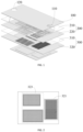
- FIG. 1 is a schematic structural diagram of a heat dissipation apparatus disclosed by an embodiment of the present application.
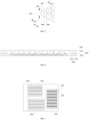
- FIG. 2 is a schematic structural diagram of a bottom board component disclosed by an embodiment of the present application.
- FIG. 3 is a schematic diagram of arrangement of flow-uniformizing channels and liquid drain channels on a flow-uniformizing component disclosed by an embodiment of the present application.
- FIG. 4 is a schematic diagram of a chip disclosed by an embodiment of the present application.
- the heat dissipation apparatus includes: a cover body 100, a flow-uniformizing component 200 and a bottom board component 300, wherein the bottom board component 300 includes a heat dissipation chamber, a plurality of heat conduction members 322 are arranged in a first region 321 of the heat dissipation chamber at a first interval, a plurality of heat conduction members 322 are arranged in a second region 323 of the heat dissipation chamber at a second interval, wherein the first interval is smaller than the second interval; the flow-uniformizing component 200 at least covers the heat dissipation chamber, a third region 201 of the flow-uniformizing component 200 includes a plurality of first flow-uniformizing channels 211 and a plurality of first liquid drain channels 212, the first flow-uniformizing channels 211 and the first liquid drain channels 212 are arranged alternately, the first flow-uniformizing channels 211
- a height of each heat conduction member 322 is smaller than a height of the heat dissipation chamber, and for example, as shown in FIG. 5 , the height h pin of each heat conduction member 322 may be 0.7 to 0.8 time the height of the heat dissipation chamber.
- a thickness of the cover body 100 may be 300-500 um, and diameters of the liquid inlet 110 and the liquid outlet 120 may be 5-8 mm.
- the plurality of first flow-uniformizing channels 211 and the plurality of first liquid drain channels 212 in the third region 201 of the flow-uniformizing component 200 may be arranged alternatively in a preset direction of the flow-uniformizing component 200, for example, the first flow-uniformizing channels 211 and the first liquid drain channels 212 are arranged in the preset direction of the flow-uniformizing component 200 according to an order of 1, 3, and 5 being the first liquid drain channels 212 and 2, 4, and 6 being the first flow-uniformizing channels 211.
- One row or a plurality of rows of liquid outlet holes may be arranged along the flow-uniformizing channels.
- the preset direction may be a direction perpendicular to a connecting line of the liquid inlet 110 and the liquid outlet 120 in the cover body 100.
- An arrangement manner of the plurality of second flow-uniformizing channels 213 and the plurality of second liquid drain channels 214 in the fourth region 202 of the flow-uniformizing component 200 is similar to an arrangement manner of the plurality of first flow-uniformizing channels 211 and the plurality of first liquid drain channels 212 in the third region 201 of the flow-uniformizing component 200, which is not repeated here.
- the cover body 100, the flow-uniformizing component 200 and the bottom board component 300 are stacked in sequence, relatively densely arranged heat conduction members 322 are arranged in the first region 321 corresponding to the high heat flux region of the chip of the bottom board component 300, such that a superficial area of the heat conduction members 322 in the first region 321 making contact with liquid is larger, relatively sparsely arranged heat conduction members 322 are arranged in the second region 323 corresponding to the low heat flux region of the chip of the bottom board component 300, such that a superficial area of the heat conduction members 322 in the second region 323 making contact with liquid is smaller, local high heat control of the chip can be implemented, at the same time, better temperature uniformity is kept, and the heat dissipation effect on the non-uniform heating chip is improved.
- the third region 201 of the flow-uniformizing component 200 corresponds to the first region 321 of the bottom board component 300
- the fourth region 202 of the flow-uniformizing component 200 corresponds to the second region 323 of the bottom board component 300
- the plurality of first flow-uniformizing channels 211 in the third region 201 of the flow-uniformizing component 200 communicate with the liquid inlet 110 in the cover body 100
- the first flow-uniformizing channels 211 are provided with the plurality of first liquid outlet holes 221 communicating with the first flow-uniformizing channels 211 and the first region 321 at a third interval
- the plurality of first liquid drain channels 212 in the third region 201 of the flow-uniformizing component 200 communicate with the first region 321 and the plurality of second flow-uniformizing channels 213 in the fourth region 202 of the flow-uniformizing component 200
- the second flow-uniformizing channels 213 are provided with the plurality of second liquid outlet holes 223 communicating with the second flow-uni
- the liquid in the first region 321 of the heat dissipation chamber flows, through the plurality of first liquid drain channels 212 arranged in the third region 201 of the flow-uniformizing component 200, into the plurality of second flow-uniformizing channels 213 arranged in the fourth region 202 of the flow-uniformizing component 200 for performing flow uniformizing, after flow uniformizing, the liquid impacts perpendicularly on the second region 323 of the heat dissipation chamber with the heat conduction members 322 through the second liquid outlet holes 223 arranged in the second flow-uniformizing channels 213 to achieve distributed flow jetting, the heat conduction members 322 make contact with the liquid to perform heat conduction, and heat dissipation of the low heat flux region (namely the sixth region 402) of the chip is achieved.
- the liquid in the second region 323 of the heat dissipation chamber flows out from the liquid outlet 120 in the cover body 100 through the plurality of second liquid drain channels 214 in the fourth region 202 of the flow-uniformizing component 200.
- the present application adopts the design of the liquid outlet holes, can improve a flow rate of the liquid flowing downwards, then improve disturbance, and enhance heat transfer.
- the heat dissipation chamber can provide a mixed flow space, prolong a flow jetting route, and enhance the heat dissipation effect.
- the liquid flowing manner that the liquid enters the heat dissipation chamber through the flow-uniformizing channels and the liquid outlet holes of the flow-uniformizing component 200, impacts on the heat conduction members 322, then is rapidly reflected, and then is drained out through the liquid drain channels can keep a lower entire pressure drop at a higher flow rate.
- the embodiment of the present application provides the heat dissipation apparatus, the relatively densely arranged heat conduction members 322 are arranged in the first region 321 of the heat dissipation chamber of the bottom board component 300, the relatively sparsely arranged heat conduction members 322 are arranged in the second region 323 of the heat dissipation chamber of the bottom board component 300, in the case where the chip is in the mounted state, the high heat flux region of the chip corresponds to the first region 321, the low heat flux region of the chip corresponds to the second region 323, in addition, the flow-uniformizing component 200 covers the heat dissipation chamber, the third region 201 of the flow-uniformizing component 200 corresponds to the first region 321 of the heat dissipation chamber, the fourth region 202 of the flow-uniformizing component 200 corresponds to the second region 323 of the heat dissipation chamber, the plurality of first flow-uniformizing channels 211 in the third region 201 of the flow-uniformizing component 200
- the heat conduction members may be microneedle teeth, adopting the microneedle teeth as the heat conduction members 322 can effectively enhance the entire heat transfer effect, and avoid the appearance of local hot spots, and meanwhile, implements better temperature control aiming at the high heat flux region.
- the microneedle teeth may be of a rectangular columnar structure, which is not specifically limited in the present application.
- an interval length among the heat conduction members 322 may be equal to a width of a bottom face of the rectangular columnar structure, that is to say, a width of a bottom face of the heat conduction members 322 arranged in the first region 321 is smaller than a width of a bottom face of the heat conduction members 322 arranged in the second region 323.
- an interval length among the heat conduction members 322 may be equal to an edge length of a bottom face square of the square columnar structure, that is to say, a bottom face square of the heat conduction members 322 arranged in the first region 321 is smaller than a bottom face square of the heat conduction members 322 arranged in the second region 323.
- a bottom face square of the heat conduction members 322 arranged in the first region 321 is smaller than a bottom face square of the heat conduction members 322 arranged in the second region 323.
- an edge length d pin of the bottom face square of the heat conduction members 322 arranged in the first region 321 may be 10-100 um
- the first interval w pin may be 10-100 um
- an edge length d pin of the bottom face square of the heat conduction members 322 arranged in the second region 323 may be 100-200 um
- the second interval w pin may be 100-200 um.
- heights of the heat conduction members 322 arranged in the first region 321 and heights of the heat conduction members 322 arranged in the second region 323 may further be arranged according to actual heat dissipation requirements, for example, the heights of the heat conduction members 322 arranged in the first region 321 are set to be larger than the heights of the heat conduction members 322 arranged in the second region 323.
- the relatively densely arranged heat conduction members 322 are arranged in the first region 321 of the heat dissipation chamber
- the relatively sparsely arranged heat conduction members 322 are arranged in the second region 323 of the heat dissipation chamber
- the third region 201 of the flow-uniformizing component 200 corresponds to the first region 321 of the heat dissipation chamber
- the fourth region 202 of the flow-uniformizing component 200 corresponds to the second region 323 of the heat dissipation chamber.
- the first liquid outlet holes 221 of the third region 201 of the flow-uniformizing component 200 being smaller than sizes of the second liquid outlet holes 223 of the fourth region 202 of the flow-uniformizing component 200, and the third interval among the first liquid outlet holes 221 being smaller than the fourth interval among the second liquid outlet holes 223, namely, the first liquid outlet holes 221 of the third region 201 are arranged densely, the second liquid outlet holes 223 of the fourth region 202 are arranged sparsely, so that the liquid outlet holes in the flow-uniformizing component 200 can be matched with the heat conduction members 322 arranged in the heat dissipation chamber, and the heat dissipation effect on the chip is further improved.
- the flow-uniformizing component 200 may include a liquid separation board 210 and a flow jetting board 220, the third region 201 of the liquid separation board 210 includes a plurality of first flow-uniformizing channels 211 and a plurality of first liquid drain channels 212, and the fourth region 202 of the liquid separation board 210 includes a plurality of second flow-uniformizing channels 213 and a plurality of second liquid drain channels 214.
- the third region 201 of the flow jetting board 220 includes a plurality of first liquid outlet holes 221 and a plurality of first liquid drain frames 222, and a fourth region 202 of the flow jetting board 220 includes a plurality of second liquid outlet holes 223 and a plurality of second liquid drain frames 224.
- the first liquid outlet holes 221 correspond to the first flow-uniformizing channels 211
- the second liquid outlet holes 223 correspond to the second flow-uniformizing channels 213
- the first liquid drain frames 222 correspond to the first liquid drain channels 212
- the first liquid drain frames 222 communicate with the first liquid drain channels 212 and the first region 321
- the second liquid drain frames 224 correspond to the second liquid drain channels 214
- the second liquid drain frames 224 communicate with the second liquid drain channels 214 and the second region 323.
- the flow-uniformizing component 200 may be composed of the liquid separation board 210 and the flow jetting board 220, a flow direction of the liquid in the liquid separation board 210 is shown in FIG. 3 , the third region 201 of the liquid separation board 210 includes the plurality of first flow-uniformizing channels 211 and the plurality of first liquid drain channels 212, the fourth region 202 of the liquid separation board 210 includes the plurality of second flow-uniformizing channels 213 and the plurality of second liquid drain channels 214, and the arrangement of the plurality of first flow-uniformizing channels 211, the plurality of first liquid drain channels 212, the plurality of second flow-uniformizing channels 213 and the plurality of second liquid drain channels 214 herein is consistent with that in the above, which is not repeated here in the present application.
- a thickness of the liquid separation board 210 may be 1-1.5 mm
- the plurality of first flow-uniformizing channels 211 may be of a rake-shaped structure
- the plurality of first liquid drain channels 212 may be of a rake-shaped structure
- the plurality of second flow-uniformizing channels 213 may be of a rake-shaped structure
- the plurality of second liquid drain channels 214 may also be of a rake-shaped structure
- a width of each flow-uniformizing channel may be 1-1.5 mm
- a width of each liquid drain channel may be 1-1.5 mm.
- a structure of the flow jetting board 220 is shown in FIG. 7 , the third region 201 of the flow jetting board 220 includes the plurality of first liquid outlet holes 221 and the plurality of first liquid drain frames 222, and the fourth region 202 of the flow jetting board 220 includes the plurality of second liquid outlet holes 223 and the plurality of second liquid drain frames 224.
- Arrangement of the first liquid outlet holes 221 corresponds to the first flow-uniformizing channels 211 of the liquid separation board 210
- arrangement of the first liquid drain frames 222 corresponds to the first liquid drain channels 212
- arrangement of the second liquid outlet holes 223 corresponds to the second flow-uniformizing channels 213 of the liquid separation board 210
- arrangement of the second liquid drain frames 224 corresponds to the second liquid drain channels 214 of the liquid separation board 210.
- a thickness of the flow jetting board 220 may be 200-300 um.
- the bottom board component 300 may include a frame board 310 and a bottom board 320, the frame board 310 is provided with the heat dissipation chamber, a plurality of heat conduction members 322 are arranged in the first region 321 of the bottom board 320 at the first interval, and a plurality of heat conduction members 322 are arranged in the second region 323 of the bottom board 320 at the second interval.
- a thickness of the bottom board 320 may be 600-800 um
- a thickness of the frame board 310 may be 200-300 um
- a height of the corresponding heat dissipation chamber may be 200-300 um.
- the bottom board 320 may be made of silicon materials. Since the chip mounted under the bottom board 320 is a silicon substrate chip, the bottom board 320 is made of the silicon materials, when the chip is welded to the heat dissipation apparatus, the problem of risk of interface reliability brought by inconsistency of coefficients of thermal expansion of the materials can be avoided.
- the bottom board 320 may be formed by etching the chip.
- an area of an arrangement region of the heat conduction members 322 on the bottom board component 300 may be larger than an area of the chip, and then heat dissipation on the chip is better implemented.
- first liquid drain channels 212 and the second liquid drain channels 214 may be strip-shaped liquid drain frames, which can improve the flow-out rate of the liquid from the first region 321 or the second region 323 of the heat dissipation chamber.
- the above heat dissipation apparatus may further include a metal layer, and the metal layer is arranged between the bottom board component 300 and the chip.
- the metal layer may be formed by sequentially plating titanium, platinum and gold on a surface of the bottom board component 300 close to the chip or on the chip surface using a vapor deposition or magnetron sputtering technology. After metallization processing is completed, gold tin solders are attached on a welding face of the bottom board component 300 or the chip using an evaporation technology, and then a clamp is used to place the heat dissipation apparatus and the chip into an atmosphere furnace for heating fit, thus achieving assembly of the heat dissipation apparatus and the chip.
- the bottom board component 300 is made of the silicon materials
- titanium in the metal layer may play a role of increasing adhesivity
- platinum in the metal layer may play a role of blocking titanium from leaking downwards
- gold may play a role of improving the weldability.
- the metal layer can separate the bottom board component 300 from the chip, avoiding the problem of risk of interface reliability brought by inconsistency of coefficients of thermal expansion of the materials.
- the heat dissipation apparatus disclosed by the present application may be entirely packaged after being assembled with the chip, that is, the heat dissipation apparatus may be directly welded on a chip silicon wafer through a patch process, then the heat dissipation apparatus and the chip are entirely packaged, so as to reduce interface thermal resistance of the heat dissipation apparatus to the chip, and the heat dissipation effect on the chip is improved.
- the heat dissipation apparatus disclosed by the present application may be used to perform heat dissipation on high-density isomerous chips, supervisor stack pointer (SSP) chips and the like.
- SSP supervisor stack pointer
- the liquid described above may be water, a dielectric working medium or a refrigerant, etc., that is, the heat dissipation apparatus disclosed by the present application may use the water, the dielectric working medium or the refrigerant as a working medium.
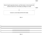
- An embodiment of the present application further discloses a method for manufacturing a heat dissipation apparatus. As shown in FIG. 8 , the manufacturing method includes:
- the cover body 100 may be bonded to the first body using epoxy resin or shadowless glue (UV glue).
- UV glue shadowless glue
- liquid separation board 210, the flow jetting board 220, the frame board 310, the bottom board 320 and the cover body 100 herein are the liquid separation board 210, the flow jetting board 220, the frame board 310, the bottom board 320 and the cover body 100 described in the heat dissipation apparatus above.
- the liquid separation board 210, the flow jetting board 220, the frame board 310 and the bottom board 320 are bonded into the first body first according to the order, then the cover body 100 is connected with the first body, a processing difficult problem of the heat dissipation apparatus in a very small space size may be solved, and the manufacturing efficiency of the heat dissipation apparatus is improved.
- the bottom board 320 and the flow jetting board 220 may be made of silicon materials
- the frame board 310 and the liquid separation board 210 may be made of glass, that is, a structure of a layer of silicon, a layer of glass, a layer of silicon and a layer of glass.
- a material of the frame board 310 may further be polydimethylsiloxane (PDMS), and the cover body 100 may be made of glass.
- the bottom board 320, the frame board 310, the flow jetting board 220, the liquid separation board 210 and the cover body 100 are processed respectively, the bottom board 320 is processed through a deep silicon etching process, the frame board 310, the liquid separation board 210 and the cover body 100 are processed through a laser cutting process, and the flow jetting board 220 is processed through an etching process.
- FIG. 9 A flowchart of processing the bottom board 320 through the deep silicon etching process is shown in FIG. 9 , including the following steps: (a) a photoetching mask board is designed according to a morphology of a needed heat conduction member; (b) spin coating of a photoresist is performed; (c) exposure is performed, and an exposure duration is changed based on a height of the needed heat conduction member; and (d) the photoresist is cleared to complete etching processing.
Landscapes
- Engineering & Computer Science (AREA)
- Microelectronics & Electronic Packaging (AREA)
- Physics & Mathematics (AREA)
- Thermal Sciences (AREA)
- Theoretical Computer Science (AREA)
- Human Computer Interaction (AREA)
- General Engineering & Computer Science (AREA)
- General Physics & Mathematics (AREA)
- Cooling Or The Like Of Semiconductors Or Solid State Devices (AREA)
- Cooling Or The Like Of Electrical Apparatus (AREA)
Abstract
Description
- The present application claims priority to
Chinese Patent Application No. 202311085306.7 filed to the Chinese Patent Office on August 25, 2023 - The present application relates to the field of heat dissipation devices, in particular to a heat dissipation apparatus and a method for manufacturing the heat dissipation apparatus.
- With the rapid development of social informatization, more requirements are put forward for the performance of electronic devices, which leads to the continuous increase of single-chip functional modules, and chips show a trend of increasing integration level and area at the same time, which makes the non-uniform power distribution of the chips become more and more obvious, resulting in a plurality of local "hot spots" of high heat flux of the chips. The temperature inhomogeneity caused by the local "hot spots" will cause thermal stress of largearea chips, resulting in chip warping and even fracture, which seriously affects the reliability and life of the chips.
- However, heat dissipation apparatuses in the related art mostly perform heat dissipation on uniform heat sources, and have a poor heat dissipation effect on non-uniform heating chips.
- The present application discloses a heat dissipation apparatus and a method for manufacturing the heat dissipation apparatus, which can improve a heat dissipation effect on non-uniform heating chips.
- In order to solve the above problem, the present application adopts the following technical solution.
- In a first aspect, an embodiment of the present application discloses a heat dissipation apparatus, including: a cover body, a flow-uniformizing component and a bottom board component, wherein the bottom board component includes a heat dissipation chamber, a plurality of heat conduction members are arranged in a first region of the heat dissipation chamber at a first interval, a plurality of heat conduction members are arranged in a second region of the heat dissipation chamber at a second interval, wherein the first interval is smaller than the second interval; the flow-uniformizing component at least covers the heat dissipation chamber, a third region of the flow-uniformizing component includes a plurality of first flow-uniformizing channels and a plurality of first liquid drain channels, the first flow-uniformizing channels and the first liquid drain channels are arranged alternately, the first flow-uniformizing channels are provided with a plurality of first liquid outlet holes at a third interval, the first liquid outlet holes communicate with the first flow-uniformizing channels and the first region, a fourth region of the flow-uniformizing component includes a plurality of second flow-uniformizing channels and a plurality of second liquid drain channels, the second flow-uniformizing channels and the second liquid drain channels are arranged alternately, the second flow-uniformizing channels are provided with a plurality of second liquid outlet holes at a fourth interval, the second liquid outlet holes communicate with the second flow-uniformizing channels and the second region, and the first liquid drain channels communicate with the first region and the second flow-uniformizing channels; the cover body covers the flow-uniformizing component, the cover body is provided with a liquid inlet and a liquid outlet, the liquid inlet communicates with the first flow-uniformizing channels, and the second liquid drain channels communicate with the second region and the liquid outlet; and in a case that a chip is in a mounted state, a face of the bottom board component away from the flow-uniformizing component makes contact with the chip, a fifth region of the chip corresponds to the first region, a sixth region of the chip corresponds to the second region, wherein a temperature of the fifth region is higher than a temperature of the sixth region.
- In a second aspect, an embodiment of the present application discloses a method for manufacturing a heat dissipation apparatus, including: bonding a liquid separation board, a flow jetting board, a frame board and a bottom board into a first body according to an order; and connecting a cover body with the first body.
- The embodiment of the present application provides the heat dissipation apparatus, relatively densely arranged heat conduction members are arranged in the first region of the heat dissipation chamber of the bottom board component, relatively sparsely arranged heat conduction members are arranged in the second region of the heat dissipation chamber of the bottom board component, in the case where the chip is in the mounted state, a high heat flux region of the chip corresponds to the first region, a low heat flux region of the chip corresponds to the second region, in addition, the flow-uniformizing component covers the heat dissipation chamber, the third region of the flow-uniformizing component corresponds to the first region of the heat dissipation chamber, the fourth region of the flow-uniformizing component corresponds to the second region of the heat dissipation chamber, the plurality of first flow-uniformizing channels in the third region of the flow-uniformizing component communicate with the liquid inlet in the cover body, the first flow-uniformizing channels are provided with the plurality of first liquid outlet holes at the third interval, the first liquid outlet holes communicate with the first flow-uniformizing channels and the first region, the plurality of first liquid drain channels in the third region of the flow-uniformizing component communicate with the first region and the plurality of second flow-uniformizing channels in the fourth region of the flow-uniformizing component, the second flow-uniformizing channels are provided with the plurality of second liquid outlet holes at the fourth interval, the second liquid outlet holes communicate with the second flow-uniformizing channels and the second region, the plurality of second liquid drain channels in the fourth region of the flow-uniformizing component communicate with the second region and the liquid outlet in the cover body, so that heat dissipation may be performed on the high heat flux region of the chip first, and then heat dissipation may be performed on the low heat flux region of the chip, thus improving the heat dissipation effect on the non-uniform heating chip. In addition, heat dissipation is performed on the chip through the heat dissipation apparatus provided by the present application, thermal stress brought by local temperature difference of the chip can be eliminated, and the service life and reliability of the chip are ensured.
-
-
FIG. 1 is a schematic structural diagram of a heat dissipation apparatus disclosed by an embodiment of the present application; -
FIG. 2 is a schematic structural diagram of a bottom board component disclosed by an embodiment of the present application; -
FIG. 3 is a schematic diagram of arrangement of flow-uniformizing channels and liquid drain channels on a flow-uniformizing component disclosed by an embodiment of the present application; -
FIG. 4 is a schematic diagram of a chip disclosed by an embodiment of the present application; -
FIG. 5 is a schematic structural diagram of a heat conduction member disclosed by an embodiment of the present application; -
FIG. 6 is a sectional view of a heat dissipation apparatus disclosed by an embodiment of the present application; -
FIG. 7 is a schematic structural diagram of a flow jetting board disclosed by an embodiment of the present application; -
FIG. 8 is a flowchart of a method for manufacturing a heat dissipation apparatus disclosed by an embodiment of the present application; and -
FIG. 9 is a flowchart of processing a bottom board disclosed by an embodiment of the present application. - Technical solutions in embodiments of the present application will be described clearly with reference to accompanying drawings in the embodiments of the present application below. Apparently, the described embodiments are part of the embodiments of the present application, not all the embodiments. Based on the embodiments of the present application, all other embodiments obtained by those ordinarily skilled in the art fall within the scope of protection of the present application.
- Terms "first", "second" and the like in the description and claims of the present application are used to distinguish similar objects, but not used to describe a specific order or sequence. It should be understood that data used like this may be interchanged where appropriate, such that the embodiments of the present application may be implemented in an order other than those illustrated or described herein, the objects distinguished by "first", "second" and the like are usually of the same class, and the number of the objects is not limited, for example, there may be one or more first objects. In addition, "and/or" in the description and claims represents at least one of connected objects, and a character "/" generally represents that front and back associated objects are in an "or" relationship.
- The present application discloses a heat dissipation apparatus and a method for manufacturing the heat dissipation apparatus.
FIG. 1 is a schematic structural diagram of a heat dissipation apparatus disclosed by an embodiment of the present application.FIG. 2 is a schematic structural diagram of a bottom board component disclosed by an embodiment of the present application.FIG. 3 is a schematic diagram of arrangement of flow-uniformizing channels and liquid drain channels on a flow-uniformizing component disclosed by an embodiment of the present application.FIG. 4 is a schematic diagram of a chip disclosed by an embodiment of the present application. - As shown in
FIG. 1 to FIG. 4 , the heat dissipation apparatus disclosed by the present application includes: acover body 100, a flow-uniformizingcomponent 200 and abottom board component 300, wherein thebottom board component 300 includes a heat dissipation chamber, a plurality ofheat conduction members 322 are arranged in afirst region 321 of the heat dissipation chamber at a first interval, a plurality ofheat conduction members 322 are arranged in asecond region 323 of the heat dissipation chamber at a second interval, wherein the first interval is smaller than the second interval; the flow-uniformizingcomponent 200 at least covers the heat dissipation chamber, athird region 201 of the flow-uniformizingcomponent 200 includes a plurality of first flow-uniformizingchannels 211 and a plurality of firstliquid drain channels 212, the first flow-uniformizingchannels 211 and the firstliquid drain channels 212 are arranged alternately, the first flow-uniformizingchannels 211 are provided with a plurality of firstliquid outlet holes 221 at a third interval, the firstliquid outlet holes 221 communicate with the first flow-uniformizingchannels 211 and thefirst region 321, afourth region 202 of the flow-uniformizingcomponent 200 includes a plurality of second flow-uniformizingchannels 213 and a plurality of secondliquid drain channels 214, the second flow-uniformizingchannels 213 and the secondliquid drain channels 214 are arranged alternately, the second flow-uniformizingchannels 213 are provided with a plurality of secondliquid outlet holes 223 at a fourth interval, the secondliquid outlet holes 223 communicate with the second flow-uniformizingchannels 213 and thesecond region 323, and the firstliquid drain channels 212 communicate with thefirst region 321 and the second flow-uniformizingchannels 213; thecover body 100 covers the flow-uniformizingcomponent 200, thecover body 100 is provided with aliquid inlet 110 and aliquid outlet 120, theliquid inlet 110 communicates with the first flow-uniformizingchannels 211, and the secondliquid drain channels 214 communicate with thesecond region 323 and theliquid outlet 120; and in a case that a chip is in a mounted state, a face of thebottom board component 300 away from the flow-uniformizingcomponent 200 makes contact with the chip, afifth region 401 of the chip corresponds to thefirst region 321, asixth region 402 of the chip corresponds to thesecond region 323, wherein a temperature of thefifth region 401 is higher than a temperature of thesixth region 402. - It needs to be noted that a height of each
heat conduction member 322 is smaller than a height of the heat dissipation chamber, and for example, as shown inFIG. 5 , the height hpin of eachheat conduction member 322 may be 0.7 to 0.8 time the height of the heat dissipation chamber. In addition, a thickness of thecover body 100 may be 300-500 um, and diameters of theliquid inlet 110 and theliquid outlet 120 may be 5-8 mm. - The plurality of first flow-uniformizing
channels 211 and the plurality of firstliquid drain channels 212 in thethird region 201 of the flow-uniformizingcomponent 200 may be arranged alternatively in a preset direction of the flow-uniformizingcomponent 200, for example, the first flow-uniformizingchannels 211 and the firstliquid drain channels 212 are arranged in the preset direction of the flow-uniformizingcomponent 200 according to an order of 1, 3, and 5 being the firstliquid drain channels 212 and 2, 4, and 6 being the first flow-uniformizingchannels 211. One row or a plurality of rows of liquid outlet holes may be arranged along the flow-uniformizing channels. For example, the preset direction may be a direction perpendicular to a connecting line of theliquid inlet 110 and theliquid outlet 120 in thecover body 100. An arrangement manner of the plurality of second flow-uniformizingchannels 213 and the plurality of secondliquid drain channels 214 in thefourth region 202 of the flow-uniformizingcomponent 200 is similar to an arrangement manner of the plurality of first flow-uniformizingchannels 211 and the plurality of firstliquid drain channels 212 in thethird region 201 of the flow-uniformizingcomponent 200, which is not repeated here. - In the present application, the
cover body 100, the flow-uniformizingcomponent 200 and thebottom board component 300 are stacked in sequence, relatively densely arrangedheat conduction members 322 are arranged in thefirst region 321 corresponding to the high heat flux region of the chip of thebottom board component 300, such that a superficial area of theheat conduction members 322 in thefirst region 321 making contact with liquid is larger, relatively sparsely arrangedheat conduction members 322 are arranged in thesecond region 323 corresponding to the low heat flux region of the chip of thebottom board component 300, such that a superficial area of theheat conduction members 322 in thesecond region 323 making contact with liquid is smaller, local high heat control of the chip can be implemented, at the same time, better temperature uniformity is kept, and the heat dissipation effect on the non-uniform heating chip is improved. - In addition, the
third region 201 of the flow-uniformizingcomponent 200 corresponds to thefirst region 321 of thebottom board component 300, thefourth region 202 of the flow-uniformizingcomponent 200 corresponds to thesecond region 323 of thebottom board component 300, the plurality of first flow-uniformizingchannels 211 in thethird region 201 of the flow-uniformizingcomponent 200 communicate with theliquid inlet 110 in thecover body 100, the first flow-uniformizingchannels 211 are provided with the plurality of firstliquid outlet holes 221 communicating with the first flow-uniformizingchannels 211 and thefirst region 321 at a third interval, the plurality of firstliquid drain channels 212 in thethird region 201 of the flow-uniformizingcomponent 200 communicate with thefirst region 321 and the plurality of second flow-uniformizingchannels 213 in thefourth region 202 of the flow-uniformizingcomponent 200, the second flow-uniformizingchannels 213 are provided with the plurality of secondliquid outlet holes 223 communicating with the second flow-uniformizingchannels 213 and thesecond region 323 at a fourth interval, the plurality of secondliquid drain channels 214 in thefourth region 202 of the flow-uniformizingcomponent 200 communicate with thesecond region 323 and theliquid outlet 120 in thecover body 100, heat dissipation may be performed on the high heat flux region of the chip first, and then heat dissipation may be performed on the low heat flux region of the chip, more uniform heat dissipation is implemented, and the heat dissipation effect on the non-uniform heating chip is further improved. - When heat dissipation is performed on the chip arranged under the
bottom board component 300 through the heat dissipation apparatus disclosed by the present application, as shown inFIG. 6 , after flowing, through theliquid inlet 110 in thecover body 100, into the plurality of first flow-uniformizingchannels 211 in thethird region 201 of the flow-uniformizingcomponent 200 for performing flow uniformizing, the liquid impacts perpendicularly on thefirst region 321 of the heat dissipation chamber with theheat conduction members 322 through the firstliquid outlet holes 221 arranged in the first flow-uniformizingchannels 211 to achieve distributed flow jetting, theheat conduction members 322 make contact with the liquid to perform heat conduction, and heat dissipation of the high heat flux region (namely the fifth region 401) of the chip is achieved. Then the liquid in thefirst region 321 of the heat dissipation chamber flows, through the plurality of firstliquid drain channels 212 arranged in thethird region 201 of the flow-uniformizingcomponent 200, into the plurality of second flow-uniformizingchannels 213 arranged in thefourth region 202 of the flow-uniformizingcomponent 200 for performing flow uniformizing, after flow uniformizing, the liquid impacts perpendicularly on thesecond region 323 of the heat dissipation chamber with theheat conduction members 322 through the secondliquid outlet holes 223 arranged in the second flow-uniformizingchannels 213 to achieve distributed flow jetting, theheat conduction members 322 make contact with the liquid to perform heat conduction, and heat dissipation of the low heat flux region (namely the sixth region 402) of the chip is achieved. After heat dissipation of the chip is completed, the liquid in thesecond region 323 of the heat dissipation chamber flows out from theliquid outlet 120 in thecover body 100 through the plurality of secondliquid drain channels 214 in thefourth region 202 of the flow-uniformizingcomponent 200. - The present application adopts the design of the liquid outlet holes, can improve a flow rate of the liquid flowing downwards, then improve disturbance, and enhance heat transfer. The heat dissipation chamber can provide a mixed flow space, prolong a flow jetting route, and enhance the heat dissipation effect. In addition, the liquid flowing manner that the liquid enters the heat dissipation chamber through the flow-uniformizing channels and the liquid outlet holes of the flow-uniformizing
component 200, impacts on theheat conduction members 322, then is rapidly reflected, and then is drained out through the liquid drain channels can keep a lower entire pressure drop at a higher flow rate. - The embodiment of the present application provides the heat dissipation apparatus, the relatively densely arranged
heat conduction members 322 are arranged in thefirst region 321 of the heat dissipation chamber of thebottom board component 300, the relatively sparsely arrangedheat conduction members 322 are arranged in thesecond region 323 of the heat dissipation chamber of thebottom board component 300, in the case where the chip is in the mounted state, the high heat flux region of the chip corresponds to thefirst region 321, the low heat flux region of the chip corresponds to thesecond region 323, in addition, the flow-uniformizingcomponent 200 covers the heat dissipation chamber, thethird region 201 of the flow-uniformizingcomponent 200 corresponds to thefirst region 321 of the heat dissipation chamber, thefourth region 202 of the flow-uniformizingcomponent 200 corresponds to thesecond region 323 of the heat dissipation chamber, the plurality of first flow-uniformizingchannels 211 in thethird region 201 of the flow-uniformizingcomponent 200 communicate with theliquid inlet 110 in thecover body 100, the first flow-uniformizingchannels 211 are provided with the plurality of firstliquid outlet holes 221 at the third interval, the firstliquid outlet holes 221 communicate with the first flow-uniformizingchannels 211 and thefirst region 321, the plurality of firstliquid drain channels 212 in thethird region 201 of the flow-uniformizingcomponent 200 communicate with thefirst region 321 and the plurality of second flow-uniformizingchannels 213 in thefourth region 202 of the flow-uniformizingcomponent 200, the second flow-uniformizingchannels 213 are provided with the plurality of secondliquid outlet holes 223 at the fourth interval, the secondliquid outlet holes 223 communicate with the second flow-uniformizingchannels 213 and thesecond region 323, the plurality of secondliquid drain channels 214 in thefourth region 202 of the flow-uniformizingcomponent 200 communicate with thesecond region 323 and theliquid outlet 120 in thecover body 100, heat dissipation can be performed on the high heat flux region of the chip first, and then heat dissipation is performed on the low heat flux region of the chip, thus improving the heat dissipation effect on the non-uniform heating chip. In addition, heat dissipation is performed on the chip through the heat dissipation apparatus provided by the present application, thermal stress brought by local temperature difference of the chip can be eliminated, and the service life and reliability of the chip are ensured. - In the present application, the heat conduction members may be microneedle teeth, adopting the microneedle teeth as the
heat conduction members 322 can effectively enhance the entire heat transfer effect, and avoid the appearance of local hot spots, and meanwhile, implements better temperature control aiming at the high heat flux region. It needs to be noted that the microneedle teeth may be of a rectangular columnar structure, which is not specifically limited in the present application. - In an implementation, in a case that the
heat conduction members 322 are of a rectangular columnar structure, an interval length among theheat conduction members 322 may be equal to a width of a bottom face of the rectangular columnar structure, that is to say, a width of a bottom face of theheat conduction members 322 arranged in thefirst region 321 is smaller than a width of a bottom face of theheat conduction members 322 arranged in thesecond region 323. In a case that theheat conduction members 322 are of a square columnar structure, an interval length among theheat conduction members 322 may be equal to an edge length of a bottom face square of the square columnar structure, that is to say, a bottom face square of theheat conduction members 322 arranged in thefirst region 321 is smaller than a bottom face square of theheat conduction members 322 arranged in thesecond region 323. For example, as shown inFIG. 5 , an edge length dpin of the bottom face square of theheat conduction members 322 arranged in thefirst region 321 may be 10-100 um, the first interval wpin may be 10-100 um, an edge length dpin of the bottom face square of theheat conduction members 322 arranged in thesecond region 323 may be 100-200 um, and the second interval wpin may be 100-200 um. In addition, heights of theheat conduction members 322 arranged in thefirst region 321 and heights of theheat conduction members 322 arranged in thesecond region 323 may further be arranged according to actual heat dissipation requirements, for example, the heights of theheat conduction members 322 arranged in thefirst region 321 are set to be larger than the heights of theheat conduction members 322 arranged in thesecond region 323. - In the embodiment of the present application, since the relatively densely arranged
heat conduction members 322 are arranged in thefirst region 321 of the heat dissipation chamber, the relatively sparsely arrangedheat conduction members 322 are arranged in thesecond region 323 of the heat dissipation chamber, thethird region 201 of the flow-uniformizingcomponent 200 corresponds to thefirst region 321 of the heat dissipation chamber, and thefourth region 202 of the flow-uniformizingcomponent 200 corresponds to thesecond region 323 of the heat dissipation chamber. By setting sizes of the firstliquid outlet holes 221 of thethird region 201 of the flow-uniformizingcomponent 200 being smaller than sizes of the secondliquid outlet holes 223 of thefourth region 202 of the flow-uniformizingcomponent 200, and the third interval among the firstliquid outlet holes 221 being smaller than the fourth interval among the secondliquid outlet holes 223, namely, the firstliquid outlet holes 221 of thethird region 201 are arranged densely, the secondliquid outlet holes 223 of thefourth region 202 are arranged sparsely, so that the liquid outlet holes in the flow-uniformizingcomponent 200 can be matched with theheat conduction members 322 arranged in the heat dissipation chamber, and the heat dissipation effect on the chip is further improved. - In an implementation, the flow-uniformizing
component 200 may include aliquid separation board 210 and aflow jetting board 220, thethird region 201 of theliquid separation board 210 includes a plurality of first flow-uniformizingchannels 211 and a plurality of firstliquid drain channels 212, and thefourth region 202 of theliquid separation board 210 includes a plurality of second flow-uniformizingchannels 213 and a plurality of secondliquid drain channels 214. Thethird region 201 of theflow jetting board 220 includes a plurality of firstliquid outlet holes 221 and a plurality of firstliquid drain frames 222, and afourth region 202 of theflow jetting board 220 includes a plurality of secondliquid outlet holes 223 and a plurality of secondliquid drain frames 224. The firstliquid outlet holes 221 correspond to the first flow-uniformizingchannels 211, the secondliquid outlet holes 223 correspond to the second flow-uniformizingchannels 213, the firstliquid drain frames 222 correspond to the firstliquid drain channels 212, the firstliquid drain frames 222 communicate with the firstliquid drain channels 212 and thefirst region 321, the secondliquid drain frames 224 correspond to the secondliquid drain channels 214, and the secondliquid drain frames 224 communicate with the secondliquid drain channels 214 and thesecond region 323. - In the present application, the flow-
uniformizing component 200 may be composed of theliquid separation board 210 and theflow jetting board 220, a flow direction of the liquid in theliquid separation board 210 is shown inFIG. 3 , thethird region 201 of theliquid separation board 210 includes the plurality of first flow-uniformizing channels 211 and the plurality of firstliquid drain channels 212, thefourth region 202 of theliquid separation board 210 includes the plurality of second flow-uniformizing channels 213 and the plurality of secondliquid drain channels 214, and the arrangement of the plurality of first flow-uniformizing channels 211, the plurality of firstliquid drain channels 212, the plurality of second flow-uniformizing channels 213 and the plurality of secondliquid drain channels 214 herein is consistent with that in the above, which is not repeated here in the present application. - For example, a thickness of the
liquid separation board 210 may be 1-1.5 mm, the plurality of first flow-uniformizing channels 211 may be of a rake-shaped structure, the plurality of firstliquid drain channels 212 may be of a rake-shaped structure, the plurality of second flow-uniformizing channels 213 may be of a rake-shaped structure, the plurality of secondliquid drain channels 214 may also be of a rake-shaped structure, a width of each flow-uniformizing channel may be 1-1.5 mm, and a width of each liquid drain channel may be 1-1.5 mm. - A structure of the
flow jetting board 220 is shown inFIG. 7 , thethird region 201 of theflow jetting board 220 includes the plurality of first liquid outlet holes 221 and the plurality of first liquid drain frames 222, and thefourth region 202 of theflow jetting board 220 includes the plurality of second liquid outlet holes 223 and the plurality of second liquid drain frames 224. Arrangement of the first liquid outlet holes 221 corresponds to the first flow-uniformizing channels 211 of theliquid separation board 210, arrangement of the first liquid drain frames 222 corresponds to the firstliquid drain channels 212, arrangement of the second liquid outlet holes 223 corresponds to the second flow-uniformizing channels 213 of theliquid separation board 210, and arrangement of the second liquid drain frames 224 corresponds to the secondliquid drain channels 214 of theliquid separation board 210. For example, a thickness of theflow jetting board 220 may be 200-300 um. - In the embodiment of the present application, the
bottom board component 300 may include aframe board 310 and abottom board 320, theframe board 310 is provided with the heat dissipation chamber, a plurality ofheat conduction members 322 are arranged in thefirst region 321 of thebottom board 320 at the first interval, and a plurality ofheat conduction members 322 are arranged in thesecond region 323 of thebottom board 320 at the second interval. - For example, a thickness of the
bottom board 320 may be 600-800 um, a thickness of theframe board 310 may be 200-300 um, and a height of the corresponding heat dissipation chamber may be 200-300 um. - In an implementation, the
bottom board 320 may be made of silicon materials. Since the chip mounted under thebottom board 320 is a silicon substrate chip, thebottom board 320 is made of the silicon materials, when the chip is welded to the heat dissipation apparatus, the problem of risk of interface reliability brought by inconsistency of coefficients of thermal expansion of the materials can be avoided. - Optionally, the
bottom board 320 may be formed by etching the chip. - In the embodiment of the present application, an area of an arrangement region of the
heat conduction members 322 on thebottom board component 300 may be larger than an area of the chip, and then heat dissipation on the chip is better implemented. - In an implementation, the first
liquid drain channels 212 and the secondliquid drain channels 214 may be strip-shaped liquid drain frames, which can improve the flow-out rate of the liquid from thefirst region 321 or thesecond region 323 of the heat dissipation chamber. - In the embodiment of the present application, the above heat dissipation apparatus may further include a metal layer, and the metal layer is arranged between the
bottom board component 300 and the chip. The metal layer may be formed by sequentially plating titanium, platinum and gold on a surface of thebottom board component 300 close to the chip or on the chip surface using a vapor deposition or magnetron sputtering technology. After metallization processing is completed, gold tin solders are attached on a welding face of thebottom board component 300 or the chip using an evaporation technology, and then a clamp is used to place the heat dissipation apparatus and the chip into an atmosphere furnace for heating fit, thus achieving assembly of the heat dissipation apparatus and the chip. - In a case that the
bottom board component 300 is made of the silicon materials, titanium in the metal layer may play a role of increasing adhesivity, platinum in the metal layer may play a role of blocking titanium from leaking downwards, and gold may play a role of improving the weldability. In a case that thebottom board component 300 is made of non-silicon materials, the metal layer can separate thebottom board component 300 from the chip, avoiding the problem of risk of interface reliability brought by inconsistency of coefficients of thermal expansion of the materials. - In addition, the heat dissipation apparatus disclosed by the present application may be entirely packaged after being assembled with the chip, that is, the heat dissipation apparatus may be directly welded on a chip silicon wafer through a patch process, then the heat dissipation apparatus and the chip are entirely packaged, so as to reduce interface thermal resistance of the heat dissipation apparatus to the chip, and the heat dissipation effect on the chip is improved.
- The heat dissipation apparatus disclosed by the present application may be used to perform heat dissipation on high-density isomerous chips, supervisor stack pointer (SSP) chips and the like.
- It needs to be noted that the liquid described above may be water, a dielectric working medium or a refrigerant, etc., that is, the heat dissipation apparatus disclosed by the present application may use the water, the dielectric working medium or the refrigerant as a working medium.
- An embodiment of the present application further discloses a method for manufacturing a heat dissipation apparatus. As shown in
FIG. 8 , the manufacturing method includes: - S820: a
liquid separation board 210, aflow jetting board 220, aframe board 310 and abottom board 320 are bonded into a first body according to an order. - S840: a cover body is connected with the first body.
- For example, the
cover body 100 may be bonded to the first body using epoxy resin or shadowless glue (UV glue). - It needs to be noted that the
liquid separation board 210, theflow jetting board 220, theframe board 310, thebottom board 320 and thecover body 100 herein are theliquid separation board 210, theflow jetting board 220, theframe board 310, thebottom board 320 and thecover body 100 described in the heat dissipation apparatus above. - Through the manufacturing method disclosed by the present application, considering size requirements of bonding, the
liquid separation board 210, theflow jetting board 220, theframe board 310 and thebottom board 320 are bonded into the first body first according to the order, then thecover body 100 is connected with the first body, a processing difficult problem of the heat dissipation apparatus in a very small space size may be solved, and the manufacturing efficiency of the heat dissipation apparatus is improved. - In the embodiment of the present application, in order to facilitate bonding of the
liquid separation board 210, theflow jetting board 220, theframe board 310 and thebottom board 320, thebottom board 320 and theflow jetting board 220 may be made of silicon materials, theframe board 310 and theliquid separation board 210 may be made of glass, that is, a structure of a layer of silicon, a layer of glass, a layer of silicon and a layer of glass. In addition, a material of theframe board 310 may further be polydimethylsiloxane (PDMS), and thecover body 100 may be made of glass. - In the present application, the
bottom board 320, theframe board 310, theflow jetting board 220, theliquid separation board 210 and thecover body 100 are processed respectively, thebottom board 320 is processed through a deep silicon etching process, theframe board 310, theliquid separation board 210 and thecover body 100 are processed through a laser cutting process, and theflow jetting board 220 is processed through an etching process. - A flowchart of processing the
bottom board 320 through the deep silicon etching process is shown inFIG. 9 , including the following steps: (a) a photoetching mask board is designed according to a morphology of a needed heat conduction member; (b) spin coating of a photoresist is performed; (c) exposure is performed, and an exposure duration is changed based on a height of the needed heat conduction member; and (d) the photoresist is cleared to complete etching processing. - Focus descriptions in the above embodiments of the present application are differences among the embodiments, different optimization features of the embodiments may be combined to form preferable embodiments as long as they are not contradictory, and given the simplicity of the text, it will not be repeated here.
- The above descriptions are only the embodiments of the present application, and are not used to limit the present application. For those skilled in the art, the present application may have various changes and variations. Any modification, equivalent replacement, improvement and the like within the spirit and principle of the present application should fall within the scope of the claims of the present application.
Claims (11)
- A heat dissipation apparatus, comprising: a cover body, a flow-uniformizing component and a bottom board component, whereinthe bottom board component comprises a heat dissipation chamber, a plurality of heat conduction members are arranged in a first region of the heat dissipation chamber at a first interval, a plurality of heat conduction members are arranged in a second region of the heat dissipation chamber at a second interval, wherein the first interval is smaller than the second interval;the flow-uniformizing component at least covers the heat dissipation chamber, a third region of the flow-uniformizing component comprises a plurality of first flow-uniformizing channels and a plurality of first liquid drain channels, the first flow-uniformizing channels and the first liquid drain channels are arranged alternately, the first flow-uniformizing channels are provided with a plurality of first liquid outlet holes at a third interval, the first liquid outlet holes communicate with the first flow-uniformizing channels and the first region, a fourth region of the flow-uniformizing component comprises a plurality of second flow-uniformizing channels and a plurality of second liquid drain channels, the second flow-uniformizing channels and the second liquid drain channels are arranged alternately, the second flow-uniformizing channels are provided with a plurality of second liquid outlet holes at a fourth interval, the second liquid outlet holes communicate with the second flow-uniformizing channels and the second region, and the first liquid drain channels communicate with the first region and the second flow-uniformizing channels;the cover body covers the flow-uniformizing component, the cover body is provided with a liquid inlet and a liquid outlet, the liquid inlet communicates with the first flow-uniformizing channels, and the second liquid drain channels communicate with the second region and the liquid outlet; andin a case that a chip is in a mounted state, a face of the bottom board component away from the flow-uniformizing component makes contact with the chip, a fifth region of the chip corresponds to the first region, a sixth region of the chip corresponds to the second region, wherein a temperature of the fifth region is higher than a temperature of the sixth region.
- The heat dissipation apparatus according to claim 1, wherein a size of each first liquid outlet hole is smaller than a size of each second liquid outlet hole, and the third interval is smaller than the fourth interval.
- The heat dissipation apparatus according to claim 1 or 2, wherein the flow-uniformizing component comprises a liquid separation board and a flow jetting board, a third region of the liquid separation board comprises the plurality of first flow-uniformizing channels and the plurality of first liquid drain channels, a fourth region of the liquid separation board comprises the plurality of second flow-uniformizing channels and the plurality of second liquid drain channels, a third region of the flow jetting board comprises the plurality of first liquid outlet holes and a plurality of first liquid drain frames, a fourth region of the flow jetting board comprises the plurality of second liquid outlet holes and a plurality of second liquid drain frames, the first liquid outlet holes correspond to the first flow-uniformizing channels, the second liquid outlet holes correspond to the second flow-uniformizing channels, the first liquid drain frames correspond to the first liquid drain channels, the first liquid drain frames communicate with the first liquid drain channels and the first region, the second liquid drain frames correspond to the second liquid drain channels, and the second liquid drain frames communicate with the second liquid drain channels and the second region.
- The heat dissipation apparatus according to claim 1, wherein the bottom board component comprises a frame board and a bottom board, the frame board is provided with the heat dissipation chamber, a plurality of heat conduction members are arranged in a first region of the bottom board at a first interval, and a plurality of heat conduction members are arranged in a second region of the bottom board at a second interval.
- The heat dissipation apparatus according to claim 4, wherein the bottom board is made of silicon materials.
- The heat dissipation apparatus according to claim 5, wherein the bottom board is formed by etching a chip.
- The heat dissipation apparatus according to claim 1, wherein an area of an arrangement region of the heat conduction members on the bottom board component is larger than an area of the chip.
- The heat dissipation apparatus according to claim 1, wherein the first liquid drain channels and the second liquid drain channels are strip-shaped liquid drain frames.
- The heat dissipation apparatus according to claim 1, further comprising a metal layer, wherein the metal layer is arranged between the bottom board component and the chip.
- A method for manufacturing a heat dissipation apparatus, comprising:bonding a liquid separation board, a flow jetting board, a frame board and a bottom board into a first body according to an order; andconnecting a cover body with the first body.
- The manufacturing method according to claim 10, wherein the bottom board and the flow jetting board are made of silicon materials, and the frame board and the liquid separation board are made of glass.
Applications Claiming Priority (2)
| Application Number | Priority Date | Filing Date | Title |
|---|---|---|---|
| CN202311085306.7A CN119517868A (en) | 2023-08-25 | 2023-08-25 | Heat dissipation device and method for manufacturing heat dissipation device |
| PCT/CN2024/093589 WO2025044302A1 (en) | 2023-08-25 | 2024-05-16 | Heat dissipation device and method for manufacturing same |
Publications (1)
| Publication Number | Publication Date |
|---|---|
| EP4567880A1 true EP4567880A1 (en) | 2025-06-11 |
Family
ID=94665133
Family Applications (1)
| Application Number | Title | Priority Date | Filing Date |
|---|---|---|---|
| EP24857457.6A Pending EP4567880A1 (en) | 2023-08-25 | 2024-05-16 | Heat dissipation device and method for manufacturing same |
Country Status (4)
| Country | Link |
|---|---|
| US (1) | US20260089880A1 (en) |
| EP (1) | EP4567880A1 (en) |
| CN (1) | CN119517868A (en) |
| WO (1) | WO2025044302A1 (en) |
Family Cites Families (5)
| Publication number | Priority date | Publication date | Assignee | Title |
|---|---|---|---|---|
| US6625025B1 (en) * | 2000-07-10 | 2003-09-23 | Nortel Networks Limited | Component cooling in electronic devices |
| CN205960170U (en) * | 2016-08-17 | 2017-02-15 | 苏州市永创金属科技有限公司 | Compound radiator of wave filter |
| CN108551750B (en) * | 2018-03-20 | 2019-09-10 | 山东超越数控电子股份有限公司 | A kind of enhancing jet stream radiator heat-dissipation efficient appliances, radiating subassembly and production method |
| TWI689698B (en) * | 2019-05-10 | 2020-04-01 | 訊凱國際股份有限公司 | Flow regulator and liquid-cooled heat sink |
| CN115696723B (en) * | 2022-10-21 | 2026-02-17 | 华为数字能源技术有限公司 | Electronic component and electronic equipment |
-
2023
- 2023-08-25 CN CN202311085306.7A patent/CN119517868A/en active Pending
-
2024
- 2024-05-16 US US19/112,612 patent/US20260089880A1/en active Pending
- 2024-05-16 EP EP24857457.6A patent/EP4567880A1/en active Pending
- 2024-05-16 WO PCT/CN2024/093589 patent/WO2025044302A1/en active Pending
Also Published As
| Publication number | Publication date |
|---|---|
| CN119517868A (en) | 2025-02-25 |
| US20260089880A1 (en) | 2026-03-26 |
| WO2025044302A1 (en) | 2025-03-06 |
Similar Documents
| Publication | Publication Date | Title |
|---|---|---|
| US8929071B2 (en) | Low cost manufacturing of micro-channel heatsink | |
| EP1768179B1 (en) | Chip cooling system | |
| US7762314B2 (en) | Cooling apparatus, cooled electronic module and methods of fabrication employing a manifold structure with interleaved coolant inlet and outlet passageways | |
| US7992627B2 (en) | Microjet module assembly | |
| US20060250773A1 (en) | Cooling apparatus, cooled electronic module and methods of fabrication thereof employing an integrated manifold and a plurality of thermally conductive fins | |
| US7362574B2 (en) | Jet orifice plate with projecting jet orifice structures for direct impingement cooling apparatus | |
| US9252069B2 (en) | High power module cooling system | |
| US20060250774A1 (en) | Cooling apparatus, cooled electronic module and methods of fabrication thereof employing an integrated coolant inlet and outlet manifold | |
| US20040190252A1 (en) | Micro-channel heat exchangers and spreaders | |
| EP2994936A1 (en) | Method for creating a selective solder seal interface for an integrated circuit cooling system | |
| US20080002363A1 (en) | Direct liquid jet impingement module for high heat flux electronics packages | |
| US11121061B2 (en) | Cooling chip structures having a jet impingement system and assembly having the same | |
| EP4567880A1 (en) | Heat dissipation device and method for manufacturing same | |
| CN117690891A (en) | Power module heat dissipation structure, heat dissipation substrate and power module | |
| US7365980B2 (en) | Micropin heat exchanger | |
| US20250227891A1 (en) | Distributed impingement and recovery manifold (dirm) cold plate | |
| EP3871477B1 (en) | Conduction cooling for circuit boards | |
| US20240096742A1 (en) | Cooling apparatus, semiconductor device including the apparatus, and manufacturing method therof | |
| WO2025001373A1 (en) | Heat dissipation device and manufacturing method for heat dissipation device | |
| CN110534436B (en) | Silicon-based self-adaptive spraying type micro-fluid heat dissipation substrate and preparation method thereof | |
| KR102897610B1 (en) | Liquid cooling structure | |
| WO2025147257A1 (en) | Distributed impingement and recovery manifold (dirm) cold plate | |
| JPH08236295A (en) | Cooled gas distribution system for plasma reactor | |
| WO2026011003A1 (en) | Liquid mems cooling system | |
| CN120704487A (en) | A memory heat dissipation module and its preparation method |
Legal Events
| Date | Code | Title | Description |
|---|---|---|---|
| STAA | Information on the status of an ep patent application or granted ep patent |
Free format text: STATUS: UNKNOWN |
|
| STAA | Information on the status of an ep patent application or granted ep patent |
Free format text: STATUS: THE INTERNATIONAL PUBLICATION HAS BEEN MADE |
|
| PUAI | Public reference made under article 153(3) epc to a published international application that has entered the european phase |
Free format text: ORIGINAL CODE: 0009012 |
|
| STAA | Information on the status of an ep patent application or granted ep patent |
Free format text: STATUS: REQUEST FOR EXAMINATION WAS MADE |
|
| 17P | Request for examination filed |
Effective date: 20250306 |
|
| AK | Designated contracting states |
Kind code of ref document: A1 Designated state(s): AL AT BE BG CH CY CZ DE DK EE ES FI FR GB GR HR HU IE IS IT LI LT LU LV MC ME MK MT NL NO PL PT RO RS SE SI SK SM TR |
|
| REG | Reference to a national code |
Ref country code: DE Ref legal event code: R079 Free format text: PREVIOUS MAIN CLASS: H01L0023473000 Ipc: H05K0007200000 |