EP4567850A1 - Contact assembly for circuit interrupters - Google Patents

Contact assembly for circuit interrupters Download PDF

Info

Publication number
EP4567850A1
EP4567850A1 EP23213881.8A EP23213881A EP4567850A1 EP 4567850 A1 EP4567850 A1 EP 4567850A1 EP 23213881 A EP23213881 A EP 23213881A EP 4567850 A1 EP4567850 A1 EP 4567850A1
Authority
EP
European Patent Office
Prior art keywords
contact
component
assembly
pieces
circuit interrupters
Prior art date
Legal status (The legal status is an assumption and is not a legal conclusion. Google has not performed a legal analysis and makes no representation as to the accuracy of the status listed.)
Pending
Application number
EP23213881.8A
Other languages
German (de)
French (fr)
Inventor
Thierry Delachaux
Christoph KENEL
Markus Hoidis
Felix Theodor Erich Rager
Matthias BATOR
Current Assignee (The listed assignees may be inaccurate. Google has not performed a legal analysis and makes no representation or warranty as to the accuracy of the list.)
ABB Schweiz AG
Original Assignee
ABB Schweiz AG
Priority date (The priority date is an assumption and is not a legal conclusion. Google has not performed a legal analysis and makes no representation as to the accuracy of the date listed.)
Filing date
Publication date
Application filed by ABB Schweiz AG filed Critical ABB Schweiz AG
Priority to EP23213881.8A priority Critical patent/EP4567850A1/en
Publication of EP4567850A1 publication Critical patent/EP4567850A1/en
Pending legal-status Critical Current

Links

Images

Classifications

    • HELECTRICITY
    • H01ELECTRIC ELEMENTS
    • H01HELECTRIC SWITCHES; RELAYS; SELECTORS; EMERGENCY PROTECTIVE DEVICES
    • H01H33/00High-tension or heavy-current switches with arc-extinguishing or arc-preventing means
    • H01H33/60Switches wherein the means for extinguishing or preventing the arc do not include separate means for obtaining or increasing flow of arc-extinguishing fluid
    • H01H33/66Vacuum switches
    • H01H33/664Contacts; Arc-extinguishing means, e.g. arcing rings
    • HELECTRICITY
    • H01ELECTRIC ELEMENTS
    • H01HELECTRIC SWITCHES; RELAYS; SELECTORS; EMERGENCY PROTECTIVE DEVICES
    • H01H33/00High-tension or heavy-current switches with arc-extinguishing or arc-preventing means
    • H01H33/60Switches wherein the means for extinguishing or preventing the arc do not include separate means for obtaining or increasing flow of arc-extinguishing fluid
    • H01H33/66Vacuum switches
    • H01H33/664Contacts; Arc-extinguishing means, e.g. arcing rings
    • H01H33/6643Contacts; Arc-extinguishing means, e.g. arcing rings having disc-shaped contacts subdivided in petal-like segments, e.g. by helical grooves
    • HELECTRICITY
    • H01ELECTRIC ELEMENTS
    • H01HELECTRIC SWITCHES; RELAYS; SELECTORS; EMERGENCY PROTECTIVE DEVICES
    • H01H33/00High-tension or heavy-current switches with arc-extinguishing or arc-preventing means
    • H01H33/60Switches wherein the means for extinguishing or preventing the arc do not include separate means for obtaining or increasing flow of arc-extinguishing fluid
    • H01H33/66Vacuum switches
    • H01H33/664Contacts; Arc-extinguishing means, e.g. arcing rings
    • H01H33/6646Contacts; Arc-extinguishing means, e.g. arcing rings having non flat disc-like contact surface

Definitions

  • Copper-Chromium alloys are known to have very good capabilities in terms of high current interruption and high voltage withstand, and are therefore normally used, e.g., in vacuum circuit breaker, when these characteristics are fundamental.
  • Silver-Tungsten Carbide alloys are known to have outstanding low chopping current characteristics and are therefore used when a low chopping current is requested.
  • WCAg in spite of the low current chopping characteristics - has the drawback of limited short-circuit current interruption capability and reproducibility (only about up to three short-circuit interruption operations can be performed in a reliable way).
  • WCAg is a relatively expensive material and its extensive use is not always convenient.
  • the proposed solutions typically involve the preparation of more or less sophisticated alloys or composite materials, the use of cladding techniques to combine materials with different properties, or similar solutions, which however are not always completely satisfactory in terms of performances of the obtained product, costs of the material(s), complexity of the production process and similar drawbacks.
  • the main aim of the present invention is to provide a contact system, in particular for vacuum interrupter applications, and more precisely for vacuum contactor applications, which allows overcoming or at least mitigating the drawbacks of the known art.
  • a purpose of the present invention is to provide a contact assembly for circuit interrupters which is capable to support different characteristics of an interrupting unit, thereby fulfilling different operative requirements.
  • a further purpose of the present invention is to provide a contact assembly for circuit interrupters, in particular for vacuum interrupters, more in particular for vacuum contactor applications, which combine efficiently low chopping currents characteristics and high current interruption characteristics.
  • a further purpose of the present invention is to provide a contact assembly for circuit interrupters which can be easily implemented into vacuum circuit interrupters, in particular into vacuum contactor applications.
  • a further purpose of the present invention is to provide a contact assembly for circuit interrupters, which has a relatively simple construction and is easy and cheap to be manufactured at industrial levels.
  • the present invention also relates to a contact arrangement which comprises a contact assembly as described herein, as well as to a circuit interrupter - in particular a vacuum circuit interrupter - comprising a contact assembly and a contact arrangement as described herein.
  • the contact assembly of the present disclosure comprises a contact element and a contact carrier.
  • the contact element comprises a first contact component which is connected to said contact carrier on one side and on an opposite side is provided with a first contact surface.
  • the contact element further comprises a second contact component which in turn comprises one or more contact pieces which are positioned on the first contact surface of said first contact component and which are at least partially positioned on the first at a distance from the center of said first contact surface.
  • the first contact component is made with a first material having relatively high current interruption characteristics and the second contact component is made with a second material having relatively low chopping current characteristics.
  • the positioning of the contact piece(s) made with a material having relatively low chopping current characteristics at discrete point(s) and at a distance from the center - and even far off the center - of the contact surface of the first contact component (which is made of a material having relatively high current interruption characteristics) brings about a contact system in which the properties of the two different materials are efficiently combined.
  • the first material forming the first contact component conveniently comprises CuCr or an alloy thereof, while the second material forming the second contact component conveniently comprises WCAg or an alloy thereof.
  • the first material may conveniently comprise an alloy or a mixture of CuCr with minor amounts of a material comprising one or more of Fe, Al, , V, Nb, Ta, Hf, Sn, Zr or Si and said second material may conveniently comprise an alloy or a mixture of WCAg with minor amounts of a material comprising one or more of Co, Fe, Bi, Sb, Te or Cu.
  • the use of the relatively expensive WCAg may be limited to a few pieces positioned on the contact surface of the first contact component, thereby contributing to relatively limit the costs of the overall contact assembly.
  • the one or more contact pieces of the second contact component at least partially protrude from the first contact surface of said first contact component and are provided with a second contact surface.
  • the current can flow through the contact material with the low chopping current performance. Then, during the opening phase, the arc starts on this material. In case of low currents, the arc burns on the material with low chopping current performance and a low chop value is thereby ensured. In case of high currents (fault conditions), the arc "moves" out of the contact pieces and is constricted on the high current interruption materials, thereby ensuring better interruption capability to the contact assembly.
  • Shape and dimensions of the contact piece(s) of the second contact component can be selected according to the needs. For instance, the shape and size (area) of the contact piece(s) may be adjusted in order to allow the contact assembly to carry the current with low electrical losses and no temperature-rise issue.
  • the second contact component may conveniently comprise a plurality of pad-shaped contact pieces which are positioned on the first contact surface of said first contact component at a distance and around the center of said first contact surface.
  • the second contact component may comprise contact pieces that extend from the center of the first contact surface into the outer portions of said first contact component.
  • Number and positioning of the pad-shaped contact pieces on the first contact surface of said first contact component can be selected according to the needs.
  • a plurality of pad-shaped contact pieces may be symmetrically positioned around the center of the first contact surface of said first contact component and at a distance from the outer edges of said first contact surface.
  • the plurality of pad-shaped contact pieces may be conveniently positioned far off the center of the first contact surface but not too close to the peripheral edge of said first contact surface.
  • the geometry of the contact pieces may vary according to the needs; for instance, the contact pieces may be rectangular or circular pads. Other geometries are however possible.
  • the thickness of the contact piece(s) of the second contact component may vary according to the needs.
  • the thickness of the contact piece(s) may be between 0.2 and 3 mm, preferably it may between 0.5 and 1.5 mm, and in more preferred embodiments between 0.8 and 1.2 mm.
  • the above dimensions may refer to the portion of the contact pieces protruding from the first contact surface.
  • shape and dimensions of the first contact component can be those typical of the contacts currently used, e.g., in vacuum interrupters, for example in vacuum contactor applications.
  • the first contact component made with high current interruption materials can conveniently comprise a disk-shaped body provided with a contact surface onto which the contact pieces made of a material with low chopping current performance are positioned as previously described.
  • the first contact component can conveniently comprise a disk-shaped body made with high current interruption materials and including a plurality of spirally-shaped cut-out portions (spiral contacts), such as, for instance, on transverse magnetic field contact in vacuum interrupters.
  • the spiral contact can be conveniently provided with a contact surface onto which the contact pieces made of a material with low chopping current performance are positioned, as in the previous case.
  • the number of contact pieces of the second contact component positioned on the contact surface of the first contact component can be equal, less or more than the number of spirally-shaped cut-out portions creating the spiral contact.
  • the disk of the first contact component may have, e.g., 3 spirally-shaped cut-out portions and 6 contact pieces positioned on the contact surface, or, vice versa, e.g., 6 spirally-shaped cut-out portions but only 4 or 3 or 2 contact pieces positioned on the contact surface.
  • the design of the first contact component can be any and do not represent a limiting feature of the present invention.
  • the contact assembly according to the present invention can be conveniently used in a contact arrangement for circuit interrupters together with a similar or different contact assembly, so as to form a contact pair that can be open and closed according to the conventional operating modes of the interrupters.
  • the positioning of the contact pieces on the contact surface of one of the contact assemblies mirrors the positioning of the contact pieces on the contact surface of the other contact assembly. In this way, in the closed position, the current can flow directly through both contact material with the low chopping current performance.
  • the contact pieces of the second contact component of one of said first or second contact assembly are in contact with the first contact surface of the first contact component of the other of said first or second contact assembly.
  • the positioning of the contact pieces on the contact surface of one of the contact assemblies is staggered with respect to the positioning of the contact pieces on the contact surface of the other contact assembly, so that - in the closed position - the second contacts surface of the contact material with the low chopping current performance of one contact assembly is in contact with the first contact surface of the first contact component of the other contact assembly with the high-short circuit interruption.
  • a circuit interrupter in particular a vacuum circuit interrupter comprising a contact arrangement as described herein is also part of the present invention.
  • the vacuum circuit interrupter of the present invention may conveniently be a vacuum contactor.
  • the present invention - in its more general definition - relates to a contact assembly 1, 10 for circuit interrupters, in particular for vacuum contactor applications.
  • the contact assembly 1, 10 comprises a contact element 2 and a contact carrier 3 which develops along and around a longitudinal axis 110 which is substantially parallel to the direction of movement of a moving contact assembly 1 or 10 of a contact arrangement 20 (see figures 11-13 ) under operating conditions, as better explained hereinafter.
  • One of the peculiar characteristics of the contact assembly 1, 10 of the invention is that it comprises a second contact component 22, 202, which in turns comprises one or more contact pieces 51, 52 that are positioned on the first contact surface 41 of the first contact component 21, 201 at a distance from the center 100 of said first contact surface 41.
  • the contact assembly 1, 10 has an axial symmetry with respect to the longitudinal axis 110 and in such a case the center 100 of the first contact surface 41 can be identified as the intersection point between the longitudinal axis 110 and the first contact surface 41 of the first contact component 21, 201.
  • the first material can be or can comprise CuCr or an alloy/composition thereof, such as, e.g., CuCr and minor amounts of a material comprising one or more of Fe, Al, Cr, V, Nb, Ta, Hf, Sn, Zr or Si.
  • the second material can be or can comprise WCAg or an alloy/composition thereof, such as, e.g., WCAg and minor amounts of a material comprising one or more of Co, Fe, Bi, Sb, Te or Cu, according to solutions known in the art.
  • the contact piece(s) 51, 52 of the second contact component 22, 202 at least partially protrude from the first contact surface 41 of the first contact component 21, 201 and are provided with a second contact surface 42.
  • the current in the closed position of the current arrangement 20 the current can flow through the contact pieces 51, 52 made with a material with the low chopping current performance.
  • the arc starts on the contact pieces 51, 52 and, in case of low currents, the arc burns on the material with low chopping current performance, thereby ensuring a low chop value.
  • high currents - such as under fault conditions - the arc "moves" out of the contact pieces 51, 52 and is constricted on the first contact surface 41 of the first contact component 21, 201 which is made with the high current interruption materials, thereby ensuring better interruption capability to the contact assembly 1, 10.
  • the second contact component 22 is substantially constituted by a ring-shaped contact piece 51 which is positioned at a certain distance around the center 100 of the first contact surface 41 of the first contact component 21, 201.
  • the second contact component 202 preferably comprises a plurality of pad-shaped contact pieces 52 which are positioned on the first contact surface 41 of the first contact component 21, 201 at a distance and around the center 100 of said first contact surface 41.
  • the plurality of the pad-shaped contact pieces 52 are symmetrically positioned far off the center 100 of the first contact surface 41 of said first contact component 21, 201, but not too close to the outer edges 410, 411 of said first contact surface 41 to avoid hindering the motion of the rotating arc.
  • the first contact component 21 is substantially constituted by a disk-shaped body 21 made with high current interruption materials.
  • the disk-shaped body 21 is provided with a contact surface 41 onto which the contact pieces (in particular a ring-shaped contact piece 51, as shown in figures 1-2 , or a plurality of pad-shaped contact pieces 52, as shown in figures 5-6 and 14 ) made of a material with low chopping current performance are positioned as previously described.
  • the first contact component 201 is substantially constituted by a disk-shaped body 201 made with high current interruption materials which includes a plurality of spirally-shaped cut-out portions 210, according to some of the so-called "spiral contact" designs of know type. Also in this case, the disk-shaped body 201 is provided with a contact surface 41 onto which the contact pieces (in particular a ring-shaped contact piece 51, as shown in figures 3-4 , or a plurality of pad-shaped contact pieces 52, as shown in figures 7-10 ) made of a material with low chopping current performance are positioned as previously described.
  • the contact pieces in particular a ring-shaped contact piece 51, as shown in figures 3-4 , or a plurality of pad-shaped contact pieces 52, as shown in figures 7-10 .
  • the design of the first contact component 21, 201 can be any according to the needs and do not represent a limiting feature of the present invention.
  • the contact arrangement 20 of the invention is substantially based on a first contact assembly 1 and a second contact assembly 10 as described herein.
  • the first 1 and second 10 contact assembly are positioned facing each other.
  • the first 1 and second 10 contact assembly are relatively movable with respect to each other along a linear direction which is substantially parallel to the longitudinal axis 110 of the contact assemblies 1, 10.
  • one of the first 1 and second 10 contact assembly is a stationary contact system while the other is a movable contact system.
  • the first 1 and second 10 contact assembly can be in closed position in which the contact elements 2 of said first 1 and second 10 contact assembly are in contact with each other or in an open position (shown in figures 11-13 ) in which the contact elements 2 of the first 1 and second 10 contact assembly are spaced apart from each other.
  • the positioning of the ring-shaped contact component 22 on the contact surface 41 of the contact assembly 1 mirrors the positioning of the ring-shaped contact component 22 on the contact surface 41 of the other contact assembly 10. From the open position shown in the figure, when the contacts are brought in the closed position (not shown) the second contact surfaces 42 of the ring-shaped contact components 22 of the two assemblies are in contact with each other and the current can flow through the through the contact material with the low chopping current performance. Similarly, with reference to figure 12 , the positioning of the pad-shaped contact pieces 52', 52", 52′′′ on the contact surface 41 of the contact assembly 1 mirrors the positioning of the pad-shaped contact pieces 52', 52", 52′′′ on the contact surface 41 of the other contact assembly 10.
  • the contact pieces 51, 52 of the second contact component 22, 202 of one of said first 1 or second 10 contact assembly are in contact with the first contact surface 41 of the first contact component 21, 201 of the other of said first 1 or second 10 contact assembly.
  • the positioning of the pad-shaped contact pieces 52', 52", 52′′′ on the contact surface 41 of the contact assembly 1 is staggered with respect to the positioning of the pad-shaped contact pieces 52', 52", 52′′′ on the contact surface 41 of the other contact assembly 10.
  • the second contact surfaces 42 of the pad-shaped contact pieces 52', 52", 52′′′ of one of the assemblies are in contact with the first contact surface 41 of the first contact component 201 of the other of contact assembly (e.g., the contact assembly 10) (similarly, the second contact surfaces 42 of the pad-shaped contact pieces 52', 52", 52′′′ of the contact assembly 10 are in contact with the first contact surface 41 of the first contact component 201 of the contact assembly 1).
  • the current can flow through the through the pieces 52', 52", 52′′′ made with the contact material with the low chopping current performance.
  • the design of the present contact assembly - which is made of two distinct materials properly positioned with respect to each other (in particular the off-center positioning of the low chopping current material at discrete points with respect to the high current interruption material) - allows combining the advantages of each material without suffering the drawbacks typical of each single material application.
  • the presently disclosed contact assembly is very easy to manufacture with consequent advantages in terms of costs.

Landscapes

  • High-Tension Arc-Extinguishing Switches Without Spraying Means (AREA)

Abstract

A contact assembly (1, 10) for circuit interrupters, which comprises a contact element (2) and a contact carrier (3). The contact element (2) comprises a first contact component (21, 201) and a second contact component (22, 202. The first contact component (21, 201) is connected to said contact carrier (3) on one side (4) and on an opposite side is provided with a first contact surface (41). The first contact component (21, 201) is made with a first material having relatively high current interruption characteristics and the second contact component (22, 202) is made with a second material having relatively low chopping current characteristics. The second contact component (22, 202) comprises one or more contact pieces (51, 52) which are at least partially positioned on the first contact surface (41) of said first contact component (21, 201) at a distance from the center (100) of said first contact surface (41).

Description

  • The present invention relates to a contact assembly for circuit interrupters. In particular, the present invention relates to an improved contact assembly for vacuum circuit interrupters, and more in particular to an improved contact assembly for vacuum contactor applications, which is capable to improve and support a number of different characteristics and requirements depending on the intended application.
  • According to solutions well known in the art, vacuum interrupters are used for breaking and making load and fault currents. Depending on the applications, the contact system has to fulfill a number of operative requirements and shall have some particular physical characteristics, such as: current interruption capability characteristics, dielectric withstand characteristics, anti-welding characteristics, low current chopping characteristics, anti-arc erosion characteristics, low contact resistance characteristics.
  • To this purpose, a number of different materials have been developed and tailored for specific applications. For instance, Copper-Chromium alloys (CuCr) are known to have very good capabilities in terms of high current interruption and high voltage withstand, and are therefore normally used, e.g., in vacuum circuit breaker, when these characteristics are fundamental. Similarly, Silver-Tungsten Carbide alloys (WCAg) are known to have outstanding low chopping current characteristics and are therefore used when a low chopping current is requested.
  • It is however extremely difficult, if not impossible, to use a single material when different requirements have to be fulfilled by the contact system, because different - and sometimes conflicting - material properties are required.
  • For instance, WCAg - in spite of the low current chopping characteristics - has the drawback of limited short-circuit current interruption capability and reproducibility (only about up to three short-circuit interruption operations can be performed in a reliable way). In addition to this drawback, it has to be noted that WCAg is a relatively expensive material and its extensive use is not always convenient.
  • Conversely, CuCr - in spite of the high current interruption characteristics (it can perform at least thirty short-circuit interruption operations at maximum short circuit current for a correctly design vacuum interrupter) - has not so good low current chopping characteristics. Thus, using a single material, in applications where both a low-chopping current and a good short-circuit current capability are required, does not provide satisfactory results.
  • Many attempts have been made in order to obtain a contact system that could combine different characteristics in order to fulfill different operative requirements.
  • The proposed solutions typically involve the preparation of more or less sophisticated alloys or composite materials, the use of cladding techniques to combine materials with different properties, or similar solutions, which however are not always completely satisfactory in terms of performances of the obtained product, costs of the material(s), complexity of the production process and similar drawbacks.
  • The main aim of the present invention is to provide a contact system, in particular for vacuum interrupter applications, and more precisely for vacuum contactor applications, which allows overcoming or at least mitigating the drawbacks of the known art.
  • Within this aim, a purpose of the present invention is to provide a contact assembly for circuit interrupters which is capable to support different characteristics of an interrupting unit, thereby fulfilling different operative requirements.
  • A further purpose of the present invention is to provide a contact assembly for circuit interrupters, in particular for vacuum interrupters, more in particular for vacuum contactor applications, which combine efficiently low chopping currents characteristics and high current interruption characteristics.
  • A further purpose of the present invention is to provide a contact assembly for circuit interrupters in which the use of relatively expensive materials is limited.
  • A further purpose of the present invention is to provide a contact assembly for circuit interrupters which can be based on the use of existing materials.
  • A further purpose of the present invention is to provide a contact assembly for circuit interrupters which can be easily implemented into vacuum circuit interrupters, in particular into vacuum contactor applications.
  • A further purpose of the present invention is to provide a contact assembly for circuit interrupters, which has a relatively simple construction and is easy and cheap to be manufactured at industrial levels.
  • The above aim and purposes, as well as other purposes that will emerge clearly from the following description and attached drawings, are provided, according to the invention, by a contact assembly, according to the following claim 1 and the related dependent claims.
  • In further aspects, the present invention also relates to a contact arrangement which comprises a contact assembly as described herein, as well as to a circuit interrupter - in particular a vacuum circuit interrupter - comprising a contact assembly and a contact arrangement as described herein.
  • In a general definition of the invention, the contact assembly of the present disclosure. comprises a contact element and a contact carrier. In details, the contact element comprises a first contact component which is connected to said contact carrier on one side and on an opposite side is provided with a first contact surface. The contact element further comprises a second contact component which in turn comprises one or more contact pieces which are positioned on the first contact surface of said first contact component and which are at least partially positioned on the first at a distance from the center of said first contact surface. Furthermore, in the contact assembly of the present disclosure, the first contact component is made with a first material having relatively high current interruption characteristics and the second contact component is made with a second material having relatively low chopping current characteristics.
  • In this way, as better described hereinafter, in the contact assembly of the present invention, the design of the contact element - and in particular of the first and of second contact components properly positioned with respect to each other - combined with the proper selection of the materials used for their manufacturing, allows obtaining an efficient combination of different characteristics, in particular high current interruption capabilities and low chopping current characteristics.
  • Indeed, it has been found that the positioning of the contact piece(s) made with a material having relatively low chopping current characteristics at discrete point(s) and at a distance from the center - and even far off the center - of the contact surface of the first contact component (which is made of a material having relatively high current interruption characteristics) brings about a contact system in which the properties of the two different materials are efficiently combined.
  • At the same time, the design of the assembly is relatively simple and the contact assembly of the present invention is therefore relatively easy to obtain from a manufacturing standpoint. The one or more contact pieces of the second contact component can be positioned on the first contact surface of the first contact component or can be at least partially housed in a corresponding seat formed on said first contact surface.
  • According to some embodiments of the contact assembly of the invention, the first material forming the first contact component conveniently comprises CuCr or an alloy thereof, while the second material forming the second contact component conveniently comprises WCAg or an alloy thereof.
  • In particular, the first material may conveniently comprise an alloy or a mixture of CuCr with minor amounts of a material comprising one or more of Fe, Al, , V, Nb, Ta, Hf, Sn, Zr or Si and said second material may conveniently comprise an alloy or a mixture of WCAg with minor amounts of a material comprising one or more of Co, Fe, Bi, Sb, Te or Cu.
  • It is also worth noting that, in the presently disclosed contact assembly, the use of the relatively expensive WCAg may be limited to a few pieces positioned on the contact surface of the first contact component, thereby contributing to relatively limit the costs of the overall contact assembly.
  • In embodiments of the contact assembly for circuit interrupters of the present disclosure, better described in the following detailed description, the one or more contact pieces of the second contact component at least partially protrude from the first contact surface of said first contact component and are provided with a second contact surface.
  • In this way, in the closed position the current can flow through the contact material with the low chopping current performance. Then, during the opening phase, the arc starts on this material. In case of low currents, the arc burns on the material with low chopping current performance and a low chop value is thereby ensured. In case of high currents (fault conditions), the arc "moves" out of the contact pieces and is constricted on the high current interruption materials, thereby ensuring better interruption capability to the contact assembly.
  • Shape and dimensions of the contact piece(s) of the second contact component can be selected according to the needs. For instance, the shape and size (area) of the contact piece(s) may be adjusted in order to allow the contact assembly to carry the current with low electrical losses and no temperature-rise issue.
  • For example, in some embodiments of the contact assembly for circuit interrupters of the invention, the second contact component may conveniently comprise a ring-shaped contact piece which is positioned around the center of the first contact surface of said first contact component.
  • Alternatively, in further embodiments of the presently disclosed contact assembly for circuit interrupters, the second contact component may conveniently comprise a plurality of pad-shaped contact pieces which are positioned on the first contact surface of said first contact component at a distance and around the center of said first contact surface.
  • In general, the second contact component may comprise contact pieces that extend from the center of the first contact surface into the outer portions of said first contact component.
  • A combination of ring-shaped and pad-shaped contact pieces properly positioned on the first contact surface of the first contact component may also be possible.
  • Number and positioning of the pad-shaped contact pieces on the first contact surface of said first contact component can be selected according to the needs.
  • For example, in exemplary embodiments of the presently disclosed contact assembly, a plurality of pad-shaped contact pieces may be symmetrically positioned around the center of the first contact surface of said first contact component and at a distance from the outer edges of said first contact surface.
  • In other words, in such embodiments, the plurality of pad-shaped contact pieces may be conveniently positioned far off the center of the first contact surface but not too close to the peripheral edge of said first contact surface.
  • The geometry of the contact pieces may vary according to the needs; for instance, the contact pieces may be rectangular or circular pads. Other geometries are however possible.
  • Similarly, the thickness of the contact piece(s) of the second contact component may vary according to the needs. Typically, the thickness of the contact piece(s) may be between 0.2 and 3 mm, preferably it may between 0.5 and 1.5 mm, and in more preferred embodiments between 0.8 and 1.2 mm. In cases where the one or more contact pieces of the second contact component at least partially protrude from the first contact surface of said first contact component, the above dimensions may refer to the portion of the contact pieces protruding from the first contact surface.
  • In the contact assembly of the present disclosure, shape and dimensions of the first contact component can be those typical of the contacts currently used, e.g., in vacuum interrupters, for example in vacuum contactor applications.
  • Thus, for instance, the first contact component made with high current interruption materials can conveniently comprise a disk-shaped body provided with a contact surface onto which the contact pieces made of a material with low chopping current performance are positioned as previously described.
  • According to other well-known designs of currently used contacts, the first contact component can conveniently comprise a disk-shaped body made with high current interruption materials and including a plurality of spirally-shaped cut-out portions (spiral contacts), such as, for instance, on transverse magnetic field contact in vacuum interrupters. Also in this case, the spiral contact can be conveniently provided with a contact surface onto which the contact pieces made of a material with low chopping current performance are positioned, as in the previous case.
  • In general, the number of contact pieces of the second contact component positioned on the contact surface of the first contact component can be equal, less or more than the number of spirally-shaped cut-out portions creating the spiral contact. For instance, the disk of the first contact component may have, e.g., 3 spirally-shaped cut-out portions and 6 contact pieces positioned on the contact surface, or, vice versa, e.g., 6 spirally-shaped cut-out portions but only 4 or 3 or 2 contact pieces positioned on the contact surface. An equal number of spirally-shaped cut-out portions and contact pieces, e.g., 3/3, is also possible.
  • In practice, the design of the first contact component can be any and do not represent a limiting feature of the present invention.
  • The contact assembly according to the present invention can be conveniently used in a contact arrangement for circuit interrupters together with a similar or different contact assembly, so as to form a contact pair that can be open and closed according to the conventional operating modes of the interrupters.
  • In a typical embodiment of a contact arrangement for circuit interrupters of the present invention, such contact arrangement may conveniently comprise a first and a second contact assembly as previously described. According to known layout of conventional contact arrangements, the first and the second contact assembly are positioned facing each other and are relatively movable (generally in a linear direction) between a closed position in which the contact elements of said first and second contact assembly are in contact with each other and an open position in which the contact elements of said first and second contact assembly are spaced apart from each other.
  • In some embodiments of the presently disclosed contact arrangement for circuit interrupters, in the closed position the contact pieces of the second contact component of said first contact assembly are in contact with the contact pieces of the second contact component of said second contact assembly.
  • In practice, as better described in the following detailed description, in these embodiments the positioning of the contact pieces on the contact surface of one of the contact assemblies mirrors the positioning of the contact pieces on the contact surface of the other contact assembly. In this way, in the closed position, the current can flow directly through both contact material with the low chopping current performance.
  • In embodiments alternative to the above described, in the closed position the contact pieces of the second contact component of one of said first or second contact assembly are in contact with the first contact surface of the first contact component of the other of said first or second contact assembly. Thus, in these embodiments the positioning of the contact pieces on the contact surface of one of the contact assemblies is staggered with respect to the positioning of the contact pieces on the contact surface of the other contact assembly, so that - in the closed position - the second contacts surface of the contact material with the low chopping current performance of one contact assembly is in contact with the first contact surface of the first contact component of the other contact assembly with the high-short circuit interruption.
  • In any case, in the closed position, the current can flow through the contact material with the low chopping current performance.
  • A circuit interrupter, in particular a vacuum circuit interrupter comprising a contact arrangement as described herein is also part of the present invention. In particular, the vacuum circuit interrupter of the present invention may conveniently be a vacuum contactor.
  • Further features and advantages of the present invention will be more apparent from the description of preferred but not exclusive embodiments of the present invention, shown by way of examples in the accompanying drawings, wherein:
    • Figure 1 is a plan view of a first embodiment of a contact assembly, according to the present invention;
    • Figure 2 is a side view of the first embodiment of a contact assembly shown in figure 1;
    • Figure 3 is a plan view of a second embodiment of a contact assembly, according to the present invention;
    • Figure 4 is a side view of the second embodiment of a contact assembly shown in figure 3;
    • Figure 5 is a plan view of a third embodiment of a contact assembly, according to the present invention;
    • Figure 6 is a side view of the third embodiment of a contact assembly shown in figure 5;
    • Figure 7 is a plan view of a fourth embodiment of a contact assembly, according to the present invention;
    • Figure 8 is a side view of the fourth embodiment of a contact assembly shown in figure 7;
    • Figure 9 is a plan view of a fifth embodiment of a contact assembly, according to the present invention;
    • Figure 10 is a plan view of a sixth embodiment of a contact assembly, according to the present invention;
    • Figure 11 is a side view of a first embodiment of a contact arrangement, according to the present invention, shown in the open position;
    • Figure 12 is a side view of a second embodiment of a contact arrangement, according to the present invention, shown in the open position;
    • Figure 13 is a side view of a third embodiment of a contact arrangement, according to the present invention, shown in the open position;
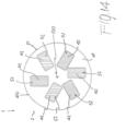
    • Figure 14 is a plan view of a seventh embodiment of a contact assembly, according to the present invention.
  • With reference to the attached figures, the present invention - in its more general definition - relates to a contact assembly 1, 10 for circuit interrupters, in particular for vacuum contactor applications.
  • According to a general mode of carrying out the present invention, the contact assembly 1, 10 comprises a contact element 2 and a contact carrier 3 which develops along and around a longitudinal axis 110 which is substantially parallel to the direction of movement of a moving contact assembly 1 or 10 of a contact arrangement 20 (see figures 11-13) under operating conditions, as better explained hereinafter.
  • In the contact assembly 1, 10 of the invention, the contact element 2 - which according to known solution can be substantially disk shaped as represented in the figures - comprises a first contact component 21, 201 which is connected to the contact carrier 3 on one side 4 and on an opposite side is provided with a first contact surface 41.
  • One of the peculiar characteristics of the contact assembly 1, 10 of the invention is that it comprises a second contact component 22, 202, which in turns comprises one or more contact pieces 51, 52 that are positioned on the first contact surface 41 of the first contact component 21, 201 at a distance from the center 100 of said first contact surface 41.
  • In particular, as shown in the figures, the contact assembly 1, 10 has an axial symmetry with respect to the longitudinal axis 110 and in such a case the center 100 of the first contact surface 41 can be identified as the intersection point between the longitudinal axis 110 and the first contact surface 41 of the first contact component 21, 201.
  • A further peculiar characteristic of the contact assembly 1, 10 of the invention is that the first contact component 21, 201 is made with a first material which have relatively high current interruption characteristics, while the second contact component 22, 202 is made with a second material which relatively low chopping current characteristics.
  • In particular, according to solutions known in the art, the first material can be or can comprise CuCr or an alloy/composition thereof, such as, e.g., CuCr and minor amounts of a material comprising one or more of Fe, Al, Cr, V, Nb, Ta, Hf, Sn, Zr or Si.
  • The second material can be or can comprise WCAg or an alloy/composition thereof, such as, e.g., WCAg and minor amounts of a material comprising one or more of Co, Fe, Bi, Sb, Te or Cu, according to solutions known in the art.
  • With particular reference to figure 2, 4, 6, and 8, in various embodiments of the contact assembly 1, 10 of the invention, the contact piece(s) 51, 52 of the second contact component 22, 202 at least partially protrude from the first contact surface 41 of the first contact component 21, 201 and are provided with a second contact surface 42.
  • Thus, according to these embodiments, in the closed position of the current arrangement 20 the current can flow through the contact pieces 51, 52 made with a material with the low chopping current performance. During the opening phase, the arc starts on the contact pieces 51, 52 and, in case of low currents, the arc burns on the material with low chopping current performance, thereby ensuring a low chop value. In case of high currents - such as under fault conditions - the arc "moves" out of the contact pieces 51, 52 and is constricted on the first contact surface 41 of the first contact component 21, 201 which is made with the high current interruption materials, thereby ensuring better interruption capability to the contact assembly 1, 10.
  • With reference to figures 1-4, in embodiments of the presently described contact assembly 1, 10, the second contact component 22 is substantially constituted by a ring-shaped contact piece 51 which is positioned at a certain distance around the center 100 of the first contact surface 41 of the first contact component 21, 201.
  • Alternatively, with reference to figures 5-10 and 14, in largely preferred embodiments of the contact assembly 1, 10 of the invention, the second contact component 202 preferably comprises a plurality of pad-shaped contact pieces 52 which are positioned on the first contact surface 41 of the first contact component 21, 201 at a distance and around the center 100 of said first contact surface 41.
  • According to further preferred embodiments of the contact assembly 1, 10 of the invention, the plurality of the pad-shaped contact pieces 52 are symmetrically positioned far off the center 100 of the first contact surface 41 of said first contact component 21, 201, but not too close to the outer edges 410, 411 of said first contact surface 41 to avoid hindering the motion of the rotating arc.
  • In the embodiments of figures 1-4 and 14, the first contact component 21 is substantially constituted by a disk-shaped body 21 made with high current interruption materials. The disk-shaped body 21 is provided with a contact surface 41 onto which the contact pieces (in particular a ring-shaped contact piece 51, as shown in figures 1-2, or a plurality of pad-shaped contact pieces 52, as shown in figures 5-6 and 14) made of a material with low chopping current performance are positioned as previously described.
  • Alternatively, with reference to figures 5-10, the first contact component 201 is substantially constituted by a disk-shaped body 201 made with high current interruption materials which includes a plurality of spirally-shaped cut-out portions 210, according to some of the so-called "spiral contact" designs of know type. Also in this case, the disk-shaped body 201 is provided with a contact surface 41 onto which the contact pieces (in particular a ring-shaped contact piece 51, as shown in figures 3-4, or a plurality of pad-shaped contact pieces 52, as shown in figures 7-10) made of a material with low chopping current performance are positioned as previously described.
  • As previously explained, the number of contact pieces 51, 52 of the second contact component 202 positioned on the contact surface 41 of the first contact component 202 can be equal, less or more than the number of spirally-shaped cut-out portions 210 creating the spiral contact. For instance, with reference to figure 9, the disk of the first contact component 201 is provided with three spirally-shaped cut-out portions 210 and six pad-shaped contact pieces 52 which are positioned on the contact surface 41; with reference to figure 10, the disk of the first contact component 201 is provided with six spirally-shaped cut-out portions 210 and three pad-shaped contact pieces 52 which are positioned on the contact surface 41 far off the center 100; with reference to figures 7-8, the disk of the first contact component 201 is provided with three spirally-shaped cut-out portions 210 and three pad-shaped contact pieces 52 which are positioned on the contact surface 41; with reference to figures 3-4, the disk of the first contact component 201 is provided with three spirally-shaped cut-out portions 210 and one single ring-shaped contact piece 51 which is positioned around the center 100 of the contact surface 41 of the first contact component 201.
  • In general, as previously said, the design of the first contact component 21, 201 can be any according to the needs and do not represent a limiting feature of the present invention. The same applies to the shape and numbers of contact pieces 51, 52 that can be tailored according to the needs.
  • With reference to figures 11-13, the present invention also relates to a contact arrangement 20 for circuit interrupters which comprises at least a contact assembly as disclosed herein.
  • In particular, according to preferred embodiments and with reference to the above-mentioned figures, the contact arrangement 20 of the invention is substantially based on a first contact assembly 1 and a second contact assembly 10 as described herein.
  • According to know solution used in current interrupters, e.g., in vacuum contactors, the first 1 and second 10 contact assembly are positioned facing each other. Typically, the first 1 and second 10 contact assembly are relatively movable with respect to each other along a linear direction which is substantially parallel to the longitudinal axis 110 of the contact assemblies 1, 10. In practice, one of the first 1 and second 10 contact assembly is a stationary contact system while the other is a movable contact system.
  • As a consequence of this movement, the first 1 and second 10 contact assembly can be in closed position in which the contact elements 2 of said first 1 and second 10 contact assembly are in contact with each other or in an open position (shown in figures 11-13) in which the contact elements 2 of the first 1 and second 10 contact assembly are spaced apart from each other.
  • In embodiments of the contact arrangement 20, in the closed position the contact pieces 51, 52 of the second contact component 22, 202 of said first contact assembly 1 are in contact with the contact pieces 51, 52 of the second contact component 22, 202 of said second contact assembly 10.
  • In practice, with reference to figure 11, in this embodiment the positioning of the ring-shaped contact component 22 on the contact surface 41 of the contact assembly 1 mirrors the positioning of the ring-shaped contact component 22 on the contact surface 41 of the other contact assembly 10. From the open position shown in the figure, when the contacts are brought in the closed position (not shown) the second contact surfaces 42 of the ring-shaped contact components 22 of the two assemblies are in contact with each other and the current can flow through the through the contact material with the low chopping current performance. Similarly, with reference to figure 12, the positioning of the pad-shaped contact pieces 52', 52", 52‴ on the contact surface 41 of the contact assembly 1 mirrors the positioning of the pad-shaped contact pieces 52', 52", 52‴ on the contact surface 41 of the other contact assembly 10. From the open position shown in the figure, when the contacts are brought in the closed position (not shown) the second contact surfaces 42 of the pad-shaped contact pieces 52', 52", 52‴ of the two assemblies are in contact with each other and also in this case the current can flow through the through the contact material (pad-shaped contact pieces 52', 52", 52‴) with the low chopping current performance.
  • In alternative embodiments of the contact arrangement 20, in the closed position the contact pieces 51, 52 of the second contact component 22, 202 of one of said first 1 or second 10 contact assembly are in contact with the first contact surface 41 of the first contact component 21, 201 of the other of said first 1 or second 10 contact assembly.
  • In practice, with reference to figure 13, the positioning of the pad-shaped contact pieces 52', 52", 52‴ on the contact surface 41 of the contact assembly 1 is staggered with respect to the positioning of the pad-shaped contact pieces 52', 52", 52‴ on the contact surface 41 of the other contact assembly 10. From the open position shown in the figure, when the contact assemblies 1, 10 are brought in the closed position (not shown) the second contact surfaces 42 of the pad-shaped contact pieces 52', 52", 52‴ of one of the assemblies (e.g., the contact assembly 1) are in contact with the first contact surface 41 of the first contact component 201 of the other of contact assembly (e.g., the contact assembly 10) (similarly, the second contact surfaces 42 of the pad-shaped contact pieces 52', 52", 52‴ of the contact assembly 10 are in contact with the first contact surface 41 of the first contact component 201 of the contact assembly 1). As in the previous cases, also in this case the current can flow through the through the pieces 52', 52", 52‴ made with the contact material with the low chopping current performance.
  • From experiments carried out with contact assemblies and contact arrangements as described above, it has been seen that the presently disclosed contact assemblies and arrangements can combine efficiently low chopping currents characteristics and high current interruption characteristics.
  • In practice, the design of the present contact assembly - which is made of two distinct materials properly positioned with respect to each other (in particular the off-center positioning of the low chopping current material at discrete points with respect to the high current interruption material) - allows combining the advantages of each material without suffering the drawbacks typical of each single material application.
  • From a manufacturing standpoint, the presently disclosed contact assembly is very easy to manufacture with consequent advantages in terms of costs.
  • It is therefore clear from the above that the contact assembly of the present disclosure, as well as the contact arrangement as described herein, fully meet the intended aims and purposes.
Claims (15)

  1. A contact assembly (1, 10) for circuit interrupters, the contact assembly (1, 10) comprising a contact element (2) and a contact carrier (3), characterized in that said contact element (2) comprises a first contact component (21, 201) and a second contact component (22, 202), wherein the first contact component (21, 201) is connected to said contact carrier (3) on one side (4) and on an opposite side is provided with a first contact surface (41), wherein the first contact component (21, 201) is made with a first material having relatively high current interruption characteristics and the second contact component (22, 202) is made with a second material having relatively low chopping current characteristics, and wherein the second contact component (22, 202) comprises one or more contact pieces (51, 52) which are at least partially positioned on the first contact surface (41) of said first contact component (21, 201) at a distance from the center (100) of said first contact surface (41).
  2. The contact assembly (1, 10) for circuit interrupters, according to claim 1, wherein said first material comprises CuCr or an alloy thereof and said second material comprises WCAg or an alloy thereof.
  3. The contact assembly (1, 10) for circuit interrupters, according to claim 1 or 2, wherein said first material comprises CuCr and minor amounts of a material comprising one or more of Fe, Al, V, Nb, Ta, Hf, Sn, Zr or Si and said second material comprises WCAg and minor amounts of a material comprising one or more of Co, Fe, Bi, Sb, Te or Cu.
  4. The contact assembly (1, 10) for circuit interrupters, according to one or more of the previous claims, wherein the one or more contact pieces (51, 52) of said second contact component (22, 202) protrudes from, are flush with or recessed into the first contact surface (41) of said first contact component (21, 201) and are provided with a second contact surface (42).
  5. The contact assembly (1, 10) for circuit interrupters, according to one or more of the previous claims, wherein the thickness of said one or more contact pieces (51, 52) of said second contact component (22, 202) is between 0.2 mm and 3 mm, preferably between 0.5 mm and 1.5 mm more preferably between 0.8 mm and 1.2 mm.
  6. The contact assembly (1, 10) for circuit interrupters, according to one or more of the previous claims, wherein said second contact component (22, 202) comprises a ring-shaped contact piece (51) positioned around the center (100) of the first contact surface (41) of said first contact component (21, 201).
  7. The contact assembly (1, 10) for circuit interrupters, according to one or more of more of the previous claims, wherein said second contact component (22, 202) comprises a plurality of pad-shaped contact pieces (52) positioned on the first contact surface (41) of said first contact component (21, 201) at a distance and around the center (100) of said first contact surface (41), said pad-shaped contact pieces (52) being made of the same or different material.
  8. The contact assembly (1, 10) for circuit interrupters, according to claim 7, wherein said plurality of pad-shaped contact pieces (52) are symmetrically positioned around the center (100) of the first contact surface (41) of said first contact component (21, 201) and at a distance from the outer edges (410, 411) of said first contact surface (41).
  9. The contact assembly (1, 10) for circuit interrupters, according to one or more of more of the previous claims, wherein said first contact component (21, 201) comprises a disk-shaped body (21).
  10. The contact assembly (1, 10) for circuit interrupters, according to one or more of more of the previous claims, wherein said first contact component (21, 201) comprises a disk-shaped body (201) including a plurality of spirally-shaped cut-out portions (210).
  11. A contact arrangement (20) for circuit interrupters comprising a contact assembly (1, 10) according to one or more of the previous claims.
  12. A contact arrangement (20) for circuit interrupters comprising a first (1) and a second (10) contact assembly according to one or more of claims 1-10, wherein said first (1) and second (2) contact assembly are positioned facing each other and are relatively movable between a closed position in which the contact elements (2) of said first (1) and (2) second contact assembly are in contact with each other and an open position in which the contact elements (2) of said first (1) and second (10) contact assembly are spaced apart from each other.
  13. A contact arrangement (20) for circuit interrupters, according to claim 12, wherein in the closed position the contact pieces (51, 52) of the second contact component (22, 202) of said first contact assembly (1) are in contact with the contact pieces (51, 52) of the second contact component (22, 202) of said second contact assembly (10).
  14. A contact arrangement (20) for circuit interrupters, according to claim 12, wherein in the closed position the contact pieces (51, 52) of the second contact component (22, 202) of one of said first (1) or second (10) contact assembly are in contact with the first contact surface (41) of the first contact component (21, 201) of the other of said first (1) or second (10) contact assembly.
  15. A circuit interrupter, in particular a vacuum circuit interrupter, comprising a contact arrangement (20) according to any of claims 11 to 14.
EP23213881.8A 2023-12-04 2023-12-04 Contact assembly for circuit interrupters Pending EP4567850A1 (en)

Priority Applications (1)

Application Number Priority Date Filing Date Title
EP23213881.8A EP4567850A1 (en) 2023-12-04 2023-12-04 Contact assembly for circuit interrupters

Applications Claiming Priority (1)

Application Number Priority Date Filing Date Title
EP23213881.8A EP4567850A1 (en) 2023-12-04 2023-12-04 Contact assembly for circuit interrupters

Publications (1)

Publication Number Publication Date
EP4567850A1 true EP4567850A1 (en) 2025-06-11

Family

ID=89076350

Family Applications (1)

Application Number Title Priority Date Filing Date
EP23213881.8A Pending EP4567850A1 (en) 2023-12-04 2023-12-04 Contact assembly for circuit interrupters

Country Status (1)

Country Link
EP (1) EP4567850A1 (en)

Citations (6)

* Cited by examiner, † Cited by third party
Publication number Priority date Publication date Assignee Title
JPH01157020A (en) * 1987-12-14 1989-06-20 Toshiba Corp Vacuum switch
JPH01173531A (en) * 1987-12-28 1989-07-10 Meidensha Corp Vacuum interrupter
JPH01204322A (en) * 1988-02-08 1989-08-16 Toshiba Corp Vacuum valve
JPH02270233A (en) * 1989-04-10 1990-11-05 Toshiba Corp Vacuum valve
EP4092708A1 (en) * 2021-05-21 2022-11-23 ABB Schweiz AG Vacuum interrupter
EP4276864A1 (en) * 2022-05-08 2023-11-15 Abb Schweiz Ag Vacuum interrupter

Patent Citations (6)

* Cited by examiner, † Cited by third party
Publication number Priority date Publication date Assignee Title
JPH01157020A (en) * 1987-12-14 1989-06-20 Toshiba Corp Vacuum switch
JPH01173531A (en) * 1987-12-28 1989-07-10 Meidensha Corp Vacuum interrupter
JPH01204322A (en) * 1988-02-08 1989-08-16 Toshiba Corp Vacuum valve
JPH02270233A (en) * 1989-04-10 1990-11-05 Toshiba Corp Vacuum valve
EP4092708A1 (en) * 2021-05-21 2022-11-23 ABB Schweiz AG Vacuum interrupter
EP4276864A1 (en) * 2022-05-08 2023-11-15 Abb Schweiz Ag Vacuum interrupter

Similar Documents

Publication Publication Date Title
US6163002A (en) Vacuum circuit interrupter with contact structure including support pins
JP5274676B2 (en) Vacuum valve
EP0133368B1 (en) High current switch contact
US20240087822A1 (en) Vacuum Interrupter
KR920006060B1 (en) Vacuum switch tube
KR0185509B1 (en) Contact electrode for vacuum interrupter
EP4276864A1 (en) Vacuum interrupter
JP3708735B2 (en) Vacuum valve
US6346683B1 (en) Vacuum interrupter and vacuum switch thereof
JP3146158B2 (en) Vacuum valve
GB2123852A (en) Electrode contacts for high current circuit interruption
JPH01128324A (en) Vacuum switch
EP4456108A1 (en) Copper compound material
CN114582685A (en) Medium voltage vacuum circuit breaker contact with improved arc extinguishing performance and related vacuum circuit breaker
JP2859394B2 (en) Contact material for vacuum valve
JP2003092050A (en) Contactor for vacuum interrupter and vacuum interrupter
JPH02270233A (en) Vacuum valve
JP7182946B2 (en) Contact material for vacuum valve, method for manufacturing contact material for vacuum valve, and vacuum valve
JPH01157020A (en) Vacuum switch
JP2019204651A (en) Vacuum valve
JPS63174232A (en) Vacuum valve
JP2881794B2 (en) Magnetically driven electrodes for vacuum interrupters
JPH06150784A (en) Vacuum valve
JP2751300B2 (en) Magnetically driven electrodes for vacuum interrupters
JPH11149855A (en) Circuit breaker

Legal Events

Date Code Title Description
PUAI Public reference made under article 153(3) epc to a published international application that has entered the european phase

Free format text: ORIGINAL CODE: 0009012

STAA Information on the status of an ep patent application or granted ep patent

Free format text: STATUS: THE APPLICATION HAS BEEN PUBLISHED

AK Designated contracting states

Kind code of ref document: A1

Designated state(s): AL AT BE BG CH CY CZ DE DK EE ES FI FR GB GR HR HU IE IS IT LI LT LU LV MC ME MK MT NL NO PL PT RO RS SE SI SK SM TR

STAA Information on the status of an ep patent application or granted ep patent

Free format text: STATUS: REQUEST FOR EXAMINATION WAS MADE

17P Request for examination filed

Effective date: 20251112

RIC1 Information provided on ipc code assigned before grant

Ipc: H01H 33/664 20060101AFI20260312BHEP

STAA Information on the status of an ep patent application or granted ep patent

Free format text: STATUS: EXAMINATION IS IN PROGRESS