EP4567776A1 - Display device - Google Patents
Display device Download PDFInfo
- Publication number
- EP4567776A1 EP4567776A1 EP22961059.7A EP22961059A EP4567776A1 EP 4567776 A1 EP4567776 A1 EP 4567776A1 EP 22961059 A EP22961059 A EP 22961059A EP 4567776 A1 EP4567776 A1 EP 4567776A1
- Authority
- EP
- European Patent Office
- Prior art keywords
- display device
- display
- filler
- controlling particles
- refractive index
- Prior art date
- Legal status (The legal status is an assumption and is not a legal conclusion. Google has not performed a legal analysis and makes no representation as to the accuracy of the status listed.)
- Pending
Links
Images



Classifications
-
- G—PHYSICS
- G09—EDUCATION; CRYPTOGRAPHY; DISPLAY; ADVERTISING; SEALS
- G09F—DISPLAYING; ADVERTISING; SIGNS; LABELS OR NAME-PLATES; SEALS
- G09F9/00—Indicating arrangements for variable information in which the information is built-up on a support by selection or combination of individual elements
- G09F9/30—Indicating arrangements for variable information in which the information is built-up on a support by selection or combination of individual elements in which the desired character or characters are formed by combining individual elements
- G09F9/302—Indicating arrangements for variable information in which the information is built-up on a support by selection or combination of individual elements in which the desired character or characters are formed by combining individual elements characterised by the form or geometrical disposition of the individual elements
- G09F9/3026—Video wall, i.e. stackable semiconductor matrix display modules
-
- C—CHEMISTRY; METALLURGY
- C09—DYES; PAINTS; POLISHES; NATURAL RESINS; ADHESIVES; COMPOSITIONS NOT OTHERWISE PROVIDED FOR; APPLICATIONS OF MATERIALS NOT OTHERWISE PROVIDED FOR
- C09K—MATERIALS FOR MISCELLANEOUS APPLICATIONS, NOT PROVIDED FOR ELSEWHERE
- C09K3/00—Materials not provided for elsewhere
- C09K3/10—Materials in mouldable or extrudable form for sealing or packing joints or covers
-
- G—PHYSICS
- G09—EDUCATION; CRYPTOGRAPHY; DISPLAY; ADVERTISING; SEALS
- G09F—DISPLAYING; ADVERTISING; SIGNS; LABELS OR NAME-PLATES; SEALS
- G09F9/00—Indicating arrangements for variable information in which the information is built-up on a support by selection or combination of individual elements
- G09F9/30—Indicating arrangements for variable information in which the information is built-up on a support by selection or combination of individual elements in which the desired character or characters are formed by combining individual elements
- G09F9/33—Indicating arrangements for variable information in which the information is built-up on a support by selection or combination of individual elements in which the desired character or characters are formed by combining individual elements being semiconductor devices, e.g. diodes
-
- C—CHEMISTRY; METALLURGY
- C09—DYES; PAINTS; POLISHES; NATURAL RESINS; ADHESIVES; COMPOSITIONS NOT OTHERWISE PROVIDED FOR; APPLICATIONS OF MATERIALS NOT OTHERWISE PROVIDED FOR
- C09K—MATERIALS FOR MISCELLANEOUS APPLICATIONS, NOT PROVIDED FOR ELSEWHERE
- C09K2200/00—Chemical nature of materials in mouldable or extrudable form for sealing or packing joints or covers
- C09K2200/02—Inorganic compounds
- C09K2200/0204—Elements
- C09K2200/0208—Carbon
-
- C—CHEMISTRY; METALLURGY
- C09—DYES; PAINTS; POLISHES; NATURAL RESINS; ADHESIVES; COMPOSITIONS NOT OTHERWISE PROVIDED FOR; APPLICATIONS OF MATERIALS NOT OTHERWISE PROVIDED FOR
- C09K—MATERIALS FOR MISCELLANEOUS APPLICATIONS, NOT PROVIDED FOR ELSEWHERE
- C09K2200/00—Chemical nature of materials in mouldable or extrudable form for sealing or packing joints or covers
- C09K2200/02—Inorganic compounds
- C09K2200/0243—Silica-rich compounds, e.g. silicates, cement, glass
- C09K2200/0247—Silica
-
- C—CHEMISTRY; METALLURGY
- C09—DYES; PAINTS; POLISHES; NATURAL RESINS; ADHESIVES; COMPOSITIONS NOT OTHERWISE PROVIDED FOR; APPLICATIONS OF MATERIALS NOT OTHERWISE PROVIDED FOR
- C09K—MATERIALS FOR MISCELLANEOUS APPLICATIONS, NOT PROVIDED FOR ELSEWHERE
- C09K2200/00—Chemical nature of materials in mouldable or extrudable form for sealing or packing joints or covers
- C09K2200/06—Macromolecular organic compounds, e.g. prepolymers
- C09K2200/0615—Macromolecular organic compounds, e.g. prepolymers obtained by reactions only involving carbon-to-carbon unsaturated bonds
- C09K2200/0632—Polystyrenes
-
- C—CHEMISTRY; METALLURGY
- C09—DYES; PAINTS; POLISHES; NATURAL RESINS; ADHESIVES; COMPOSITIONS NOT OTHERWISE PROVIDED FOR; APPLICATIONS OF MATERIALS NOT OTHERWISE PROVIDED FOR
- C09K—MATERIALS FOR MISCELLANEOUS APPLICATIONS, NOT PROVIDED FOR ELSEWHERE
- C09K2200/00—Chemical nature of materials in mouldable or extrudable form for sealing or packing joints or covers
- C09K2200/06—Macromolecular organic compounds, e.g. prepolymers
- C09K2200/0645—Macromolecular organic compounds, e.g. prepolymers obtained otherwise than by reactions involving carbon-to-carbon unsaturated bonds
- C09K2200/065—Polyurethanes
-
- C—CHEMISTRY; METALLURGY
- C09—DYES; PAINTS; POLISHES; NATURAL RESINS; ADHESIVES; COMPOSITIONS NOT OTHERWISE PROVIDED FOR; APPLICATIONS OF MATERIALS NOT OTHERWISE PROVIDED FOR
- C09K—MATERIALS FOR MISCELLANEOUS APPLICATIONS, NOT PROVIDED FOR ELSEWHERE
- C09K2200/00—Chemical nature of materials in mouldable or extrudable form for sealing or packing joints or covers
- C09K2200/06—Macromolecular organic compounds, e.g. prepolymers
- C09K2200/068—Containing also other elements than carbon, oxygen or nitrogen in the polymer main chain
- C09K2200/0685—Containing silicon
-
- H—ELECTRICITY
- H10—SEMICONDUCTOR DEVICES; ELECTRIC SOLID-STATE DEVICES NOT OTHERWISE PROVIDED FOR
- H10K—ORGANIC ELECTRIC SOLID-STATE DEVICES
- H10K59/00—Integrated devices, or assemblies of multiple devices, comprising at least one organic light-emitting element covered by group H10K50/00
- H10K59/10—OLED displays
- H10K59/18—Tiled displays
Definitions
- the present disclosure relates to a display device.
- Recent display devices tend to have a plurality of display modules comprising display panels disposed together to form a large-sized screen.
- a display device can implement a large-size screen by combining a plurality of display panels.
- An object of the present embodiment is to provide a display device capable of minimizing heterogeneity between adjacent display modules.
- a display device comprises a plurality of display modules disposed in a vertical direction and a left and right direction; and a filler filled between adjacent display modules, in which the filler comprises a binder resin, transmittance-controlling particles, and refractive index-controlling particles.
- the binder resin may comprise at least one of organic polysiloxane, polysiloxane block copolymer, polyester urethane, and wax.
- a viscosity of the binder resin may be 50,000 cPs to 300,000 cPs.
- the transmittance-controlling particles may comprise carbon black and color controlling particles (color pigments).
- the refractive index-controlling particles may comprise silica and polystyrene beads.
- the size of the silica may be 5 nm to 10 nm.
- the size of the polystyrene beads may be 10 nm to 90 nm.
- the content ratio of the transmittance-controlling particles may be 2% to 30%.
- the content ratio of the refractive index-controlling particles may be 10% to 40%.
- the display module may comprise a substrate; a plurality of LED chips disposed on the substrate; a coating layer covering the plurality of LED chips; and an optical film covering the coating layer.
- the binder resin may comprise at least one of organic polysiloxane, polysiloxane block copolymer, polyester urethane, and wax.
- the transmittance-controlling particles may comprise carbon black and color controlling particles (color pigments).
- the refractive index-controlling particles may comprise silica and polystyrene beads.
- the filler between adjacent display modules can minimize optical distortion caused by steps between a plurality of display modules and gaps between a plurality of display modules.
- the colors of a plurality of display modules can be matched by the transmittance controlling particles, and light scattered between a plurality of display modules can be absorbed.
- optical distortion due to refractive index can be minimized by refractive index-controlling particles.
- the display device is, for example, an intelligent display device that adds a computer support function to a broadcast reception function, and while remaining faithful to the broadcast reception function, the display device can have an Internet function or the like and can have a more convenient interface such as a manual input device, a touch screen, or a space remote control.
- the display device can be accessed to the Internet and a computer, and can also perform functions such as e-mail, web browsing, banking, or games.
- a standardized general-purpose OS can be used for these various functions.
- the display device described in the present disclosure can perform various user-friendly functions, for example, since various applications can be freely added or deleted on a general-purpose OS kernel. More specifically, the display device can be, for example, a network TV, an HBBTV, a smart TV, an LED TV, an OLED TV, or the like, and in some cases, can also be applied to a smartphone.
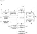
- FIG. 1 is a block diagram illustrating the configuration of a display device according to the present embodiment.
- the display device 100 may comprise a broadcast receiving part 130, an external device interface 135, a memory 140, a user input interface 150, a controller 170, a wireless communication interface 173, a display 180, a speaker 185, and a power supply circuit 190.
- the broadcast receiving part 130 may comprise a tuner 131, a demodulator 132, and a network interface 133.
- the tuner 131 can select a specific broadcast channel according to a channel selection command.
- the tuner 131 can receive a broadcast signal for the selected specific broadcast channel.
- a demodulator 132 can separate a received broadcast signal into a video signal, an audio signal, and a data signal related to a broadcast program, and can restore the separated video signal, audio signal, and data signal into a form that can be output.
- the external device interface 135 can receive an application or a list of applications within an adjacent external device and transmit them to the controller 170 or memory 140.
- the external device interface 135 can provide a connection path between the display device 100 and the external device.
- the external device interface 135 can receive one or more of images and audio output from an external device connected wirelessly or wiredly to the display device 100 and transmit them to the controller 170.
- the external device interface 135 can comprise a plurality of external input terminals.
- the plurality of external input terminals can comprise an RGB terminal, one or more HDMI (High Definition Multimedia Interface) terminals, and a component terminal.
- An image signal of an external device input through an external device interface 135 can be output through a display 180.
- a voice signal of an external device input through an external device interface 135 can be output through a speaker 185.
- An external device that can be connected to the external device interface 135 may be any one of a set-top box, a Blu-ray player, a DVD player, a game console, a sound bar, a smartphone, a PC, a USB memory, and a home theater, but these are only examples.
- the network interface 133 can provide an interface for connecting the display device 100 to a wired/wireless network comprising the Internet.
- the network interface 133 can transmit or receive data to or from another user or another electronic device through the accessed network or another network linked to the accessed network.
- some of the content data stored in the display device 100 can be transmitted to a selected user or electronic device among other users or other electronic devices pre-registered in the display device 100.
- the network interface 133 can access a predetermined web page through an accessed network or another network linked to the accessed network. In other words, the network interface can access a predetermined web page through a network and transmit or receive data with the corresponding server.
- the network interface 133 can receive content or data provided by a content provider or a network operator.
- the network interface 133 can receive content such as movies, advertisements, games, VOD, broadcast signals, or the like, and information related thereto provided from a content provider or a network provider through a network.
- the network interface 133 can receive firmware update information and update files provided by the network operato, and transmit data to the Internet or content provider or network operator.
- the network interface 133 can select and receive a desired application from among applications open to the public via a network.
- the memory 140 stores programs for each signal processing and control within the controller 170 and can store signal processed images, voices, or data signals.
- the memory 140 may perform a function for temporary storage of image, voice, or data signals input from an external device interface 135 or a network interface 133, and may also store information about a specific image through a channel memory function.
- the memory 140 can store an application or a list of applications input from an external device interface 135 or a network interface 133.
- the display device 100 can play content files (moving image files, still image files, music files, document files, application files, or the like) stored in the memory 140 and provide them to the user.
- content files moving image files, still image files, music files, document files, application files, or the like
- the user input interface 150 can transmit a signal input by the user to the controller 170, or transmit a signal from the controller 170 to the user.
- the user input interface 150 can receive and process control signals such as power on/off, channel selection, and screen setting from the remote control device 200 according to various communication methods such as Bluetooth, Ultra Wideband (WB), ZigBee, RF (Radio Frequency) communication, or infrared (IR) communication, or process control signals from the controller 170 to be transmitted to the remote control device 200.
- the user input interface 150 can transmit control signals input from local keys (not illustrated) such as a power key, channel key, volume key, and setting key to the controller 170.
- local keys such as a power key, channel key, volume key, and setting key
- An image signal processed by the controller 170 may be input to the display 180 and displayed as an image corresponding to the image signal.
- an image signal processed by the controller 170 may be input to an external output device through an external device interface 135.
- the voice signal processed in the controller 170 can be output as audio to the speaker 185. Additionally, the voice signal processed in the controller 170 can be input to an external output device through the external device interface 135.
- controller 170 can control the overall operation within the display device 100.
- controller 170 can control the display device 100 by a user command or an internal program input through the user input interface 150, and can access to a network to allow the user to download a desired application or application list into the display device 100.
- the controller 170 enables the user-selected channel information or the like to be output through the display 180 or speaker 185 together with the processed image or audio signal.
- controller 170 allows an image signal or voice signal from an external device, for example, a camera or camcorder, input through the external device interface 135 to be output through the display 180 or speaker 185 in accordance with an external device image playback command received through the user input interface 150.
- an external device for example, a camera or camcorder
- the controller 170 can control the display 180 to display an image, and for example, can control the display 180 to display a broadcast image input through the tuner 131, an external input image input through the external device interface 135, an image input through the network interface part, or an image stored in the memory 140.
- the image displayed on the display 180 can be a still image or a moving image, and can be a 2D image or a 3D image.
- controller 170 can control the playback of content stored in the display device 100, received broadcast content, or external input content input from the outside, and the content can be in various forms such as broadcast images, external input images, audio files, still images, accessed web screens, and document files.
- the wireless communication interface 173 can perform communication with an external device through wired or wireless communication.
- the wireless communication interface 173 can perform short range communication with an external device.
- the wireless communication interface 173 can support short range communication by using at least one of Bluetooth TM , RFID (Radio Frequency Identification), Infrared Data Association (IrDA), UWB (Ultra Wideband), ZigBee, NFC (Near Field Communication), Wi-Fi (Wireless-Fidelity), Wi-Fi Direct, and Wireless USB (Wireless Universal Serial Bus) technologies.
- Such a wireless communication interface 173 can support wireless communication between the display device 100 and a wireless communication system, between the display device 100 and another display device 100, or between the display device 100 and a network where the display device 100 (or an external server) is located via a wireless area network.
- the wireless area network can be a wireless personal area network.
- the other display device 100 may be a wearable device (e.g., a smartwatch, smart glass, HMD (head mounted display)), a mobile terminal such as a smart phone, etc., which can exchange data with (or be linked to) the display device 100 according to the present disclosure.
- the wireless communication interface 173 may detect (or recognize) a wearable device capable of communication around the display device 100.
- the controller 170 can transmit at least a part of the data processed in the display device 100 to the wearable device via the wireless communication interface 173. Accordingly, a user of the wearable device can use the data processed in the display device 100 via the wearable device.
- the display 180 can generate a driving signal by converting an image signal, data signal, OSD signal processed by the controller 170 or an image signal, data signal, or the like received from an external device interface 135 into R, G, and B signals, respectively.
- the display device 100 illustrated in FIG. 1 is only an embodiment of the present disclosure, some of the illustrated components may be integrated, added, or omitted according to the specifications of the display device 100 actually implemented.
- two or more components may be combined into one component, or one component may be divided into two or more components, as needed.
- the functions performed by each block are intended to explain an embodiment of the present disclosure, and the specific operations or devices thereof do not limit the scope of the present disclosure.
- the display device 100 may receive and play back an image through a network interface 133 or an external device interface 135 without having a tuner 131 and a demodulator 132.
- the display device 100 may be implemented separately as an image processing device, such as a set-top box for receiving contents according to broadcast signals or various network services, and a content playback device for playing contents input from the image processing device.
- an image processing device such as a set-top box for receiving contents according to broadcast signals or various network services
- a content playback device for playing contents input from the image processing device.
- a method for operating the display device according to the embodiment of the present disclosure to be described below may be performed by any one of the display device 100 described with reference to FIG. 1 , as well as an image processing device such as the separated set-top box, or a content playback device having a display 180 and an audio output part 185.
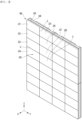
- FIG. 2 is a perspective view illustrating a plurality of display modules according to the present embodiment
- FIG. 3 is a cross-sectional view illustrating a space filled with filler between adjacent display modules illustrated in FIG. 2
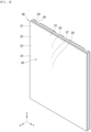
- FIG. 4 is a perspective view illustrating a space filled with filler between adjacent display modules as illustrated in FIG. 2 ;
- a display device 100 particularly a display 180, may comprise a display module 202.
- the display module 202 may comprise a substrate 210, a plurality of LED chips 211, 212, 213, a coating layer 214, and an optical film 215.
- a circuit connected to a plurality of LED chips 211, 212, 213 may be provided on the substrate 210.
- the substrate 210 may be a printed circuit board (PCB).
- a plurality of LED chips 211, 212, 213 may be disposed on a substrate 210.
- the plurality of LED chips 211, 212, 213 may comprise an R LED chip 211, a G LED chip 212, and a B LED chip 213.
- a plurality of the R LED chips 211, G LED chips 212, and B LED chips 213 may be provided in multiples on the substrate 210, respectively.
- the coating layer 214 can cover a plurality of LED chips 211, 212, 213 and can cover a surface of the substrate 210 on which the LED chips 211, 212, 213 are disposed.
- the coating layer 214 can support the LED chips 211, 212, 213 and protect the LED chips 211, 212, 213 and the substrate 210.
- the optical film 215 can cover the coating layer 214.
- the optical film 215 can be disposed on the front surface of the coating layer 214 and can protect the coating layer 214.
- a plurality of display modules 202 may be provided.
- a plurality of display modules 221, 222, 223, 224, 225, 226, 227, 228 can be disposed in a vertical direction Z and a left and right direction Y, and the plurality of display modules 221, 222, 223, 224, 225, 226, 227, 228 can provide one screen together or can provide a plurality of screens by dividing them.
- a plurality of display modules 221, 222, 223, 224, 225, 226, 227, 228 can be formed with the same structure, and the common configuration is described as a display module 202.
- the display device 100 may further comprise a module holder 230 in which a plurality of display modules 202 are mounted, and a cabinet 240 in which the module holder 230 is mounted.
- the module holder 230 may be formed larger than the display module 202, and a plurality of display modules 202 may be disposed on the front surface of the module holder 230.
- the module holder 230 can be disposed on the front surface of the cabinet 240, or can be disposed inside the cabinet 240.
- the cabinet 240 can support the module holder 230 and protect the module holder 230.
- a plurality of display modules 202 be disposed on one plane without steps, but minute steps between modules may occur due to errors in the manufacturing process or during the assembly process.
- the step between modules may cause a bright line to appear when the display module 202 is turned on due to the step, and may cause a white line (i.e., a white colored line) due to the protrusion of a specific display module when the display module 202 is turned off, which may reduce the sense of unity.
- a white line i.e., a white colored line
- the plurality of display modules 202 be disposed so that the gap G between adjacent display modules is minimized, but a slight gap G may exist between adjacent display modules.
- the gap G may be equal to or larger than a certain size (for example, 40 ⁇ m), in which case, when the display module 202 is turned on, a dark line may occur due to the light-off, and when the display module 202 is turned off, a white line may occur due to optical distortion (that is, scattering and refractive index deviation) in the gap G.
- a certain size for example, 40 ⁇ m
- the display device 100 may further comprise a filler 250 filled in the gap G between adjacent display modules.
- the filler 250 may comprise a binder resin 260, a transmittance-controlling particle 270, and a refractive index-controlling particle 280.
- binder resin 260 may comprise at least one of organic polysiloxan, polysiloxan block copolymer, polyester urethane, and high viscosity wax.
- the viscosity of the binder resin 260 can be 50,000 cPs to 300,000 cPs.
- Examples of the transmittance-controlling particles 270 may comprise carbon black for controlling transmittance and color, and color controlling particles (color pigments).
- color-controlling particles As examples of color-controlling particles, cobalt, titanium dioxide (TiO2), or the like can be applied.
- the transmittance-controlling particles 270 can match colors between display modules 202 and absorb scattered light.
- the refractive index-controlling particles 280 may comprise silica and polystyrene beads, as an example.
- the size of the silica may be from 5 nm to 10 nm, and the size of the polystyrene beads may be from 10 nm to 90 nm.
- Refractive index-controlling particles 280 can prevent optical distortion due to refractive index.
- the content ratio of the binder resin 260 may be 30% to 88%, the content ratio of the transmittance controlling particles 270 may be 2% to 30%, and the content ratio of the refractive index-controlling particles 280 may be 10% to 40%.
- each particle When dispersed, each particle can have a uniform dispersion of polystyrene beads 3.0 or less.
- the filler 250 can be filled in the gap G of the plurality of display modules 202 and can be cured in the gap G.
- the filler 250 can absorb light scattered from the gap G and provide an optical sense of identity between the gap G and the display module 202.
- the filler 250 can provide a the sense of unity to the plurality of display modules 202 as if the plurality of display modules 202 were one display module, as illustrated in FIG. 4 .
- FIG. 5 is a diagram illustrating a manufacturing process of a display device according to the present embodiment
- FIG. 6 is a cross-sectional view illustrating a plurality of display modules illustrated in FIG. 5
- FIG. 7 is a diagram illustrating a method for manufacturing a display device according to the present embodiment.
- a method for manufacturing a display device may comprise a step of applying a filler 250 between adjacent display modules 202 (S1, hereinafter referred to as an applying step), a step of filling the filler 250 using a tool T (S2, hereinafter referred to as a filling step), and a step of wiping off the filler 250' from the surface of adjacent display modules 202 (S3, hereinafter referred to as a cleaning step).
- the filler 250 can be applied to the gap G between adjacent display modules 202, as illustrated in FIG. 5 (a) .
- the filler 250 may comprise a binder resin 260, a transmittance-controlling particle 270, and a refractive index-controlling particle 280, as illustrated in FIG. 3 .
- a worker or robot can apply filler 250 to the gap G using an application mechanism C.
- the application mechanism C may comprise a cartridge containing a filler 250 therein and a nozzle disposed at the outlet of the cartridge.
- Cartridges can be manufactured and applied in different sizes according to capacity and can be configured to be suitable for mass production.
- the nozzle be configured to inject filler 250 between assembled display modules 202.
- the gap G may be smaller than the outlet of the nozzle, and a worker or robot may apply filler 250 to the gap and surrounding area of the display module G, as illustrated in FIG. 6 (a) and FIG. 7 (a).
- a part of the filler 250 may penetrate the gap G, and the remainder of the filler 250 may not flow into the gap G and remain on the front surface of the display module 202.
- the filling step (S2) may be a step of pushing the fillerl 250 for which the application step (S1) has been completed into the gap G, or may be a step of filling the gap G with the filling material 250.
- the worker or robot can move the tool T along the gap G.
- a part that is not filled in the gap G can be moved to the gap G by being pushed by the tool T in Fig. 6 (b) and Fig. 7 (b).
- the gap G can be minimized, and the maximum amount of filler 250 can be filled into the gap G.
- the remainder 250' of the filler 250 may remain on the front surface of the display module 202, as illustrated in FIG. 7 (b).
- a worker, a robot, or the like can clean the surface of the filler 250' of the surfaces of adjacent display modules 202 with a cleaning member, and the filler 250 filled in the gap G can be cured (e.g., naturally cured).
- the display device can have the gap G of the display modules 202 hidden by the filler 250, and the display device can secure a sense of unity.
Landscapes
- Engineering & Computer Science (AREA)
- Physics & Mathematics (AREA)
- General Physics & Mathematics (AREA)
- Theoretical Computer Science (AREA)
- Chemical & Material Sciences (AREA)
- Multimedia (AREA)
- Materials Engineering (AREA)
- Organic Chemistry (AREA)
- Devices For Indicating Variable Information By Combining Individual Elements (AREA)
Abstract
Description
- The present disclosure relates to a display device.
- Recent display devices tend to have a plurality of display modules comprising display panels disposed together to form a large-sized screen.
- A display device can implement a large-size screen by combining a plurality of display panels.
- An example of a display device having a plurality of display panels disposed is disclosed in
Korean Patent Publication No. 10-2016-0097599 A (published on August 18, 2016 - An object of the present embodiment is to provide a display device capable of minimizing heterogeneity between adjacent display modules.
- A display device according to the present disclosure comprises a plurality of display modules disposed in a vertical direction and a left and right direction; and a filler filled between adjacent display modules, in which the filler comprises a binder resin, transmittance-controlling particles, and refractive index-controlling particles.
- The binder resin may comprise at least one of organic polysiloxane, polysiloxane block copolymer, polyester urethane, and wax.
- A viscosity of the binder resin may be 50,000 cPs to 300,000 cPs.
- The transmittance-controlling particles may comprise carbon black and color controlling particles (color pigments).
- The refractive index-controlling particles may comprise silica and polystyrene beads.
- The size of the silica may be 5 nm to 10 nm.
- The size of the polystyrene beads may be 10 nm to 90 nm.
- The content ratio of the transmittance-controlling particles may be 2% to 30%.
- The content ratio of the refractive index-controlling particles may be 10% to 40%.
- The display module may comprise a substrate; a plurality of LED chips disposed on the substrate; a coating layer covering the plurality of LED chips; and an optical film covering the coating layer.
- A method for manufacturing a display device according to the present disclosure comprises applying a filler between adjacent display modules; filling with the filler using a tool; and wiping off the filler from the surfaces of the adjacent display modules; in which the filler may comprise a binder resin, transmittance-controlling particles, and refractive index-controlling particles.
- The binder resin may comprise at least one of organic polysiloxane, polysiloxane block copolymer, polyester urethane, and wax.
- The transmittance-controlling particles may comprise carbon black and color controlling particles (color pigments).
- The refractive index-controlling particles may comprise silica and polystyrene beads.
- According to the present embodiment, the filler between adjacent display modules can minimize optical distortion caused by steps between a plurality of display modules and gaps between a plurality of display modules.
- In addition, the colors of a plurality of display modules can be matched by the transmittance controlling particles, and light scattered between a plurality of display modules can be absorbed.
- Additionally, optical distortion due to refractive index can be minimized by refractive index-controlling particles.
-
-
FIG. 1 is a block diagram illustrating the configuration of a display device according to the present embodiment; -
FIG. 2 is a perspective view illustrating a plurality of display modules according to the present embodiment; -
FIG. 3 is a cross-sectional view illustrating a space filled with filler between adjacent display modules illustrated inFIG. 2 ; -
FIG. 4 is a perspective view illustrating a space filled with filler between adjacent display modules as illustrated inFIG. 2 ; -
FIG. 5 is a diagram illustrating a manufacturing process of a display device according to the present embodiment; -
FIG. 6 is a cross-sectional view illustrating a plurality of display modules illustrated inFIG. 5 ; and -
FIG. 7 is a diagram illustrating a method for manufacturing a display device according to the present embodiment. - Hereinafter, embodiments related to the present disclosure will be described in more detail with reference to the drawings. The suffixes "interface," "module," and "part" used for components in the following description are given or used interchangeably only for the convenience of writing the specification, and do not have distinct meanings or roles in themselves.
- The display device according to an embodiment of the present disclosure is, for example, an intelligent display device that adds a computer support function to a broadcast reception function, and while remaining faithful to the broadcast reception function, the display device can have an Internet function or the like and can have a more convenient interface such as a manual input device, a touch screen, or a space remote control. In addition, with the support of a wired or wireless Internet function, it can be accessed to the Internet and a computer, and can also perform functions such as e-mail, web browsing, banking, or games. A standardized general-purpose OS can be used for these various functions.
- Accordingly, the display device described in the present disclosure can perform various user-friendly functions, for example, since various applications can be freely added or deleted on a general-purpose OS kernel. More specifically, the display device can be, for example, a network TV, an HBBTV, a smart TV, an LED TV, an OLED TV, or the like, and in some cases, can also be applied to a smartphone.
-
FIG. 1 is a block diagram illustrating the configuration of a display device according to the present embodiment. - Referring to
FIG. 1 , thedisplay device 100 may comprise abroadcast receiving part 130, anexternal device interface 135, amemory 140, auser input interface 150, acontroller 170, awireless communication interface 173, adisplay 180, aspeaker 185, and apower supply circuit 190. - The
broadcast receiving part 130 may comprise atuner 131, ademodulator 132, and anetwork interface 133. - The
tuner 131 can select a specific broadcast channel according to a channel selection command. Thetuner 131 can receive a broadcast signal for the selected specific broadcast channel. - A
demodulator 132 can separate a received broadcast signal into a video signal, an audio signal, and a data signal related to a broadcast program, and can restore the separated video signal, audio signal, and data signal into a form that can be output. - The
external device interface 135 can receive an application or a list of applications within an adjacent external device and transmit them to thecontroller 170 ormemory 140. - The
external device interface 135 can provide a connection path between thedisplay device 100 and the external device. Theexternal device interface 135 can receive one or more of images and audio output from an external device connected wirelessly or wiredly to thedisplay device 100 and transmit them to thecontroller 170. Theexternal device interface 135 can comprise a plurality of external input terminals. The plurality of external input terminals can comprise an RGB terminal, one or more HDMI (High Definition Multimedia Interface) terminals, and a component terminal. - An image signal of an external device input through an
external device interface 135 can be output through adisplay 180. A voice signal of an external device input through anexternal device interface 135 can be output through aspeaker 185. - An external device that can be connected to the
external device interface 135 may be any one of a set-top box, a Blu-ray player, a DVD player, a game console, a sound bar, a smartphone, a PC, a USB memory, and a home theater, but these are only examples. - The
network interface 133 can provide an interface for connecting thedisplay device 100 to a wired/wireless network comprising the Internet. Thenetwork interface 133 can transmit or receive data to or from another user or another electronic device through the accessed network or another network linked to the accessed network. - In addition, some of the content data stored in the
display device 100 can be transmitted to a selected user or electronic device among other users or other electronic devices pre-registered in thedisplay device 100. - The
network interface 133 can access a predetermined web page through an accessed network or another network linked to the accessed network. In other words, the network interface can access a predetermined web page through a network and transmit or receive data with the corresponding server. - In addition, the
network interface 133 can receive content or data provided by a content provider or a network operator. In other words, thenetwork interface 133 can receive content such as movies, advertisements, games, VOD, broadcast signals, or the like, and information related thereto provided from a content provider or a network provider through a network. - Additionally, the
network interface 133 can receive firmware update information and update files provided by the network operato, and transmit data to the Internet or content provider or network operator. - The
network interface 133 can select and receive a desired application from among applications open to the public via a network. - The
memory 140 stores programs for each signal processing and control within thecontroller 170 and can store signal processed images, voices, or data signals. - In addition, the
memory 140 may perform a function for temporary storage of image, voice, or data signals input from anexternal device interface 135 or anetwork interface 133, and may also store information about a specific image through a channel memory function. - The
memory 140 can store an application or a list of applications input from anexternal device interface 135 or anetwork interface 133. - The
display device 100 can play content files (moving image files, still image files, music files, document files, application files, or the like) stored in thememory 140 and provide them to the user. - The
user input interface 150 can transmit a signal input by the user to thecontroller 170, or transmit a signal from thecontroller 170 to the user. For example, theuser input interface 150 can receive and process control signals such as power on/off, channel selection, and screen setting from theremote control device 200 according to various communication methods such as Bluetooth, Ultra Wideband (WB), ZigBee, RF (Radio Frequency) communication, or infrared (IR) communication, or process control signals from thecontroller 170 to be transmitted to theremote control device 200. - In addition, the
user input interface 150 can transmit control signals input from local keys (not illustrated) such as a power key, channel key, volume key, and setting key to thecontroller 170. - An image signal processed by the
controller 170 may be input to thedisplay 180 and displayed as an image corresponding to the image signal. In addition, an image signal processed by thecontroller 170 may be input to an external output device through anexternal device interface 135. - The voice signal processed in the
controller 170 can be output as audio to thespeaker 185. Additionally, the voice signal processed in thecontroller 170 can be input to an external output device through theexternal device interface 135. - In addition, the
controller 170 can control the overall operation within thedisplay device 100. - In addition, the
controller 170 can control thedisplay device 100 by a user command or an internal program input through theuser input interface 150, and can access to a network to allow the user to download a desired application or application list into thedisplay device 100. - The
controller 170 enables the user-selected channel information or the like to be output through thedisplay 180 orspeaker 185 together with the processed image or audio signal. - In addition, the
controller 170 allows an image signal or voice signal from an external device, for example, a camera or camcorder, input through theexternal device interface 135 to be output through thedisplay 180 orspeaker 185 in accordance with an external device image playback command received through theuser input interface 150. - Meanwhile, the
controller 170 can control thedisplay 180 to display an image, and for example, can control thedisplay 180 to display a broadcast image input through thetuner 131, an external input image input through theexternal device interface 135, an image input through the network interface part, or an image stored in thememory 140. In this case, the image displayed on thedisplay 180 can be a still image or a moving image, and can be a 2D image or a 3D image. - In addition, the
controller 170 can control the playback of content stored in thedisplay device 100, received broadcast content, or external input content input from the outside, and the content can be in various forms such as broadcast images, external input images, audio files, still images, accessed web screens, and document files. - The
wireless communication interface 173 can perform communication with an external device through wired or wireless communication. Thewireless communication interface 173 can perform short range communication with an external device. To this end, thewireless communication interface 173 can support short range communication by using at least one of Bluetooth™, RFID (Radio Frequency Identification), Infrared Data Association (IrDA), UWB (Ultra Wideband), ZigBee, NFC (Near Field Communication), Wi-Fi (Wireless-Fidelity), Wi-Fi Direct, and Wireless USB (Wireless Universal Serial Bus) technologies. Such awireless communication interface 173 can support wireless communication between thedisplay device 100 and a wireless communication system, between thedisplay device 100 and anotherdisplay device 100, or between thedisplay device 100 and a network where the display device 100 (or an external server) is located via a wireless area network. The wireless area network can be a wireless personal area network. - Here, the
other display device 100 may be a wearable device (e.g., a smartwatch, smart glass, HMD (head mounted display)), a mobile terminal such as a smart phone, etc., which can exchange data with (or be linked to) thedisplay device 100 according to the present disclosure. Thewireless communication interface 173 may detect (or recognize) a wearable device capable of communication around thedisplay device 100. - Furthermore, if the detected wearable device is a device authenticated to communicate with the
display device 100 according to the present disclosure, thecontroller 170 can transmit at least a part of the data processed in thedisplay device 100 to the wearable device via thewireless communication interface 173. Accordingly, a user of the wearable device can use the data processed in thedisplay device 100 via the wearable device. - The
display 180 can generate a driving signal by converting an image signal, data signal, OSD signal processed by thecontroller 170 or an image signal, data signal, or the like received from anexternal device interface 135 into R, G, and B signals, respectively. - Meanwhile, since the
display device 100 illustrated inFIG. 1 is only an embodiment of the present disclosure, some of the illustrated components may be integrated, added, or omitted according to the specifications of thedisplay device 100 actually implemented. - In other words, two or more components may be combined into one component, or one component may be divided into two or more components, as needed. In addition, the functions performed by each block are intended to explain an embodiment of the present disclosure, and the specific operations or devices thereof do not limit the scope of the present disclosure.
- According to another embodiment of the present disclosure, unlike as illustrated in
FIG. 1 , thedisplay device 100 may receive and play back an image through anetwork interface 133 or anexternal device interface 135 without having atuner 131 and ademodulator 132. - For example, the
display device 100 may be implemented separately as an image processing device, such as a set-top box for receiving contents according to broadcast signals or various network services, and a content playback device for playing contents input from the image processing device. - In this case, a method for operating the display device according to the embodiment of the present disclosure to be described below may be performed by any one of the
display device 100 described with reference toFIG. 1 , as well as an image processing device such as the separated set-top box, or a content playback device having adisplay 180 and anaudio output part 185. -
FIG. 2 is a perspective view illustrating a plurality of display modules according to the present embodiment,FIG. 3 is a cross-sectional view illustrating a space filled with filler between adjacent display modules illustrated inFIG. 2 , andFIG. 4 is a perspective view illustrating a space filled with filler between adjacent display modules as illustrated inFIG. 2 ; - A
display device 100, particularly adisplay 180, may comprise adisplay module 202. - The
display module 202 may comprise asubstrate 210, a plurality ofLED chips coating layer 214, and anoptical film 215. - A circuit connected to a plurality of
LED chips substrate 210. Thesubstrate 210 may be a printed circuit board (PCB). - A plurality of
LED chips substrate 210. The plurality ofLED chips R LED chip 211, aG LED chip 212, and aB LED chip 213. - A plurality of the
R LED chips 211, G LED chips 212, and B LED chips 213 may be provided in multiples on thesubstrate 210, respectively. - The
coating layer 214 can cover a plurality ofLED chips substrate 210 on which theLED chips coating layer 214 can support theLED chips LED chips substrate 210. - The
optical film 215 can cover thecoating layer 214. Theoptical film 215 can be disposed on the front surface of thecoating layer 214 and can protect thecoating layer 214. - A plurality of
display modules 202 may be provided. - A plurality of
display modules display modules - A plurality of
display modules display module 202. - The
display device 100, particularly thedisplay 180, may further comprise amodule holder 230 in which a plurality ofdisplay modules 202 are mounted, and acabinet 240 in which themodule holder 230 is mounted. - The
module holder 230 may be formed larger than thedisplay module 202, and a plurality ofdisplay modules 202 may be disposed on the front surface of themodule holder 230. - The
module holder 230 can be disposed on the front surface of thecabinet 240, or can be disposed inside thecabinet 240. - The
cabinet 240 can support themodule holder 230 and protect themodule holder 230. - It is preferable that a plurality of
display modules 202 be disposed on one plane without steps, but minute steps between modules may occur due to errors in the manufacturing process or during the assembly process. - The step between modules may cause a bright line to appear when the
display module 202 is turned on due to the step, and may cause a white line (i.e., a white colored line) due to the protrusion of a specific display module when thedisplay module 202 is turned off, which may reduce the sense of unity. - It is preferable that the plurality of
display modules 202 be disposed so that the gap G between adjacent display modules is minimized, but a slight gap G may exist between adjacent display modules. - The gap G may be equal to or larger than a certain size (for example, 40 µm), in which case, when the
display module 202 is turned on, a dark line may occur due to the light-off, and when thedisplay module 202 is turned off, a white line may occur due to optical distortion (that is, scattering and refractive index deviation) in the gap G. - It is desirable for the
display device 100 to minimize bright lines and white lines, and thedisplay device 100, particularly thedisplay 180, may further comprise afiller 250 filled in the gap G between adjacent display modules. - The
filler 250 may comprise abinder resin 260, a transmittance-controllingparticle 270, and a refractive index-controllingparticle 280. - Examples of the
binder resin 260 may comprise at least one of organic polysiloxan, polysiloxan block copolymer, polyester urethane, and high viscosity wax. - The viscosity of the
binder resin 260 can be 50,000 cPs to 300,000 cPs. - Examples of the transmittance-controlling
particles 270 may comprise carbon black for controlling transmittance and color, and color controlling particles (color pigments). - As examples of color-controlling particles, cobalt, titanium dioxide (TiO2), or the like can be applied.
- The transmittance-controlling
particles 270 can match colors betweendisplay modules 202 and absorb scattered light. - The refractive index-controlling
particles 280 may comprise silica and polystyrene beads, as an example. - The size of the silica may be from 5 nm to 10 nm, and the size of the polystyrene beads may be from 10 nm to 90 nm.
- Refractive index-controlling
particles 280 can prevent optical distortion due to refractive index. - The content ratio of the
binder resin 260 may be 30% to 88%, the content ratio of thetransmittance controlling particles 270 may be 2% to 30%, and the content ratio of the refractive index-controllingparticles 280 may be 10% to 40%. - When dispersed, each particle can have a uniform dispersion of polystyrene beads 3.0 or less.
- After mounting the plurality of
display modules 202, thefiller 250 can be filled in the gap G of the plurality ofdisplay modules 202 and can be cured in the gap G. - The
filler 250 can absorb light scattered from the gap G and provide an optical sense of identity between the gap G and thedisplay module 202. - The
filler 250 can provide a the sense of unity to the plurality ofdisplay modules 202 as if the plurality ofdisplay modules 202 were one display module, as illustrated inFIG. 4 . -
FIG. 5 is a diagram illustrating a manufacturing process of a display device according to the present embodiment,FIG. 6 is a cross-sectional view illustrating a plurality of display modules illustrated inFIG. 5 , andFIG. 7 is a diagram illustrating a method for manufacturing a display device according to the present embodiment. - A method for manufacturing a display device may comprise a step of applying a
filler 250 between adjacent display modules 202 (S1, hereinafter referred to as an applying step), a step of filling thefiller 250 using a tool T (S2, hereinafter referred to as a filling step), and a step of wiping off the filler 250' from the surface of adjacent display modules 202 (S3, hereinafter referred to as a cleaning step). - During the application step, the
filler 250 can be applied to the gap G betweenadjacent display modules 202, as illustrated inFIG. 5 (a) . - The
filler 250 may comprise abinder resin 260, a transmittance-controllingparticle 270, and a refractive index-controllingparticle 280, as illustrated inFIG. 3 . - During the application step, a worker or robot can apply
filler 250 to the gap G using an application mechanism C. - The application mechanism C may comprise a cartridge containing a
filler 250 therein and a nozzle disposed at the outlet of the cartridge. - Cartridges can be manufactured and applied in different sizes according to capacity and can be configured to be suitable for mass production.
- It is preferable that the nozzle be configured to inject
filler 250 between assembleddisplay modules 202. - The gap G may be smaller than the outlet of the nozzle, and a worker or robot may apply
filler 250 to the gap and surrounding area of the display module G, as illustrated inFIG. 6 (a) and FIG. 7 (a). - A part of the
filler 250 may penetrate the gap G, and the remainder of thefiller 250 may not flow into the gap G and remain on the front surface of thedisplay module 202. - The filling step (S2) may be a step of pushing the
fillerl 250 for which the application step (S1) has been completed into the gap G, or may be a step of filling the gap G with the fillingmaterial 250. - During the filling step (S2), the worker or robot can move the tool T along the gap G.
- In the application step (S1) of the
filler 250, a part that is not filled in the gap G can be moved to the gap G by being pushed by the tool T inFig. 6 (b) and Fig. 7 (b). - By the filling step (S2), the gap G can be minimized, and the maximum amount of
filler 250 can be filled into the gap G. - During the charging step (S2), the remainder 250' of the
filler 250 may remain on the front surface of thedisplay module 202, as illustrated in FIG. 7 (b). - During the cleaning step (S3), a worker, a robot, or the like can clean the surface of the filler 250' of the surfaces of
adjacent display modules 202 with a cleaning member, and thefiller 250 filled in the gap G can be cured (e.g., naturally cured). - As described above, when the application step (S1), the filling step (S2), and the cleaning step (S3) are completed, the display device can have the gap G of the
display modules 202 hidden by thefiller 250, and the display device can secure a sense of unity. - The above description is merely an example of the technical idea of the present disclosure, and those skilled in the art will appreciate that various modifications and variations may be made without departing from the essential characteristics of the present disclosure.
- Accordingly, the embodiments disclosed in the present disclosure are not intended to limit the technical idea of the present disclosure but to explain it, and the scope of the technical idea of the present disclosure is not limited by these embodiments.
- The scope of protection of the present disclosure should be interpreted by the claims below, and all technical ideas within a scope equivalent thereto should be interpreted as being comprised in the scope of the rights of the present disclosure.
Claims (12)
- A display device comprising:a plurality of display modules disposed in a vertical direction and a left and right direction; anda filler filled between adjacent display modules,wherein the filler comprises a binder resin, transmittance-controlling particles, and refractive index-controlling particles.
- The display device of claim 1,
wherein the binder resin comprises at least one of organic polysiloxane, polysiloxane block copolymer, polyester urethane, or wax. - The display device of claim 1,
wherein a viscosity of the binder resin is 50,000 cPs to 300,000 cPs. - The display device of claim 1,
wherein the transmittance-controlling particles comprise carbon black and color controlling particles (color pigments). - The display device of claim 1,
wherein the refractive index-controlling particles comprise silica and polystyrene beads. - The display device of claim 1,wherein a size of the silica is 5 nm to 10 nm, andwherein a size of the polystyrene beads is 10 nm to 90 nm.
- The display device of claim 1,wherein a content ratio of the transmittance-controlling particles is 2% to 30%, andwherein a content ratio of the refractive index-controlling particles is 10% to 40%.
- The display device of claim 1,
wherein the display module comprises:a substrate;a plurality of LED chips disposed on the substrate;a coating layer covering the plurality of LED chips; andan optical film covering the coating layer. - A method for manufacturing display device, comprising:applying a filler between adjacent display modules;filling with the filler using a tool; andwiping off the filler from surfaces of the adjacent display modules; andwherein the filler comprises a binder resin, transmittance-controlling particles, and refractive index-controlling particles.
- A display device of claim 9,
wherein the binder resin comprises at least one of organic polysiloxane, polysiloxane block copolymer, polyester urethane, or wax. - A display device of claim 9,
wherein the transmittance-controlling particles comprise carbon black and color controlling particles (color pigments). - A display device of claim 9,
wherein the refractive index-controlling particles comprise silica and polystyrene beads.
Applications Claiming Priority (1)
| Application Number | Priority Date | Filing Date | Title |
|---|---|---|---|
| PCT/KR2022/014347 WO2024071456A1 (en) | 2022-09-26 | 2022-09-26 | Display device |
Publications (2)
| Publication Number | Publication Date |
|---|---|
| EP4567776A1 true EP4567776A1 (en) | 2025-06-11 |
| EP4567776A4 EP4567776A4 (en) | 2025-10-22 |
Family
ID=90478279
Family Applications (1)
| Application Number | Title | Priority Date | Filing Date |
|---|---|---|---|
| EP22961059.7A Pending EP4567776A4 (en) | 2022-09-26 | 2022-09-26 | DISPLAY DEVICE |
Country Status (3)
| Country | Link |
|---|---|
| EP (1) | EP4567776A4 (en) |
| KR (1) | KR20250078423A (en) |
| WO (1) | WO2024071456A1 (en) |
Family Cites Families (9)
| Publication number | Priority date | Publication date | Assignee | Title |
|---|---|---|---|---|
| JP3815374B2 (en) * | 2002-05-20 | 2006-08-30 | 株式会社デンソー | EL display device |
| JP4698660B2 (en) * | 2006-12-12 | 2011-06-08 | サムスンコーニング精密素材株式会社 | External light shielding film for display device, manufacturing method thereof, and filter for display device including the same |
| KR102272059B1 (en) | 2015-02-09 | 2021-07-05 | 삼성전자주식회사 | Display module and display device comprising the same |
| JP6411685B1 (en) * | 2017-10-12 | 2018-10-24 | ルーメンス カンパニー リミテッド | LED module assembly for display |
| KR102231786B1 (en) * | 2018-12-19 | 2021-03-25 | (주)탑나노시스 | Composition of repairing solution for working stage, method of repairing the working stage |
| US11424224B2 (en) * | 2019-04-24 | 2022-08-23 | Seoul Viosys Co., Ltd. | LED display panel, LED display apparatus having the same and method of fabricating the same |
| KR102800894B1 (en) * | 2019-09-23 | 2025-04-29 | 삼성전자주식회사 | Display appartus and manufacturing method thereof |
| CN113540325B (en) * | 2020-04-22 | 2023-11-03 | 群创光电股份有限公司 | electronic device |
| KR102788991B1 (en) * | 2020-05-12 | 2025-03-31 | 삼성디스플레이 주식회사 | Tiled display device |
-
2022
- 2022-09-26 WO PCT/KR2022/014347 patent/WO2024071456A1/en not_active Ceased
- 2022-09-26 KR KR1020257001286A patent/KR20250078423A/en active Pending
- 2022-09-26 EP EP22961059.7A patent/EP4567776A4/en active Pending
Also Published As
| Publication number | Publication date |
|---|---|
| KR20250078423A (en) | 2025-06-02 |
| EP4567776A4 (en) | 2025-10-22 |
| WO2024071456A1 (en) | 2024-04-04 |
Similar Documents
| Publication | Publication Date | Title |
|---|---|---|
| CN102769725B (en) | Image display, portable terminal and operate its method | |
| US9749575B1 (en) | Display device and operating method thereof | |
| AU2008335654B2 (en) | Remote control protocol for media systems controlled by portable devices | |
| EP3417630B1 (en) | Display device and operating method thereof | |
| CA2749515C (en) | Television capable of implementing function extension | |
| KR102230024B1 (en) | Electronic device, and method for operating the same | |
| US20020008779A1 (en) | Audio/video system and function-extending module therefor | |
| EP3430814B1 (en) | Display device and method of operating the same | |
| US10481753B2 (en) | Display device and method of operating the same | |
| CN101489057A (en) | Television function expansion component using golden finger connector | |
| JP5389195B2 (en) | Information processing system, portable terminal, and information processing method | |
| EP4567776A1 (en) | Display device | |
| CN102780866A (en) | Modularized television | |
| KR102384520B1 (en) | Display device and controlling method thereof | |
| KR102269276B1 (en) | Electronic device, and method for operating the same | |
| KR20200084563A (en) | Display device, and controlling method thereof | |
| US9825961B2 (en) | Method and apparatus for assigning devices to a media service | |
| CN101489058A (en) | Control method for implementing television set function expansion | |
| CN205754693U (en) | A kind of integration of three networks is live/VOD system | |
| CN101489060B (en) | Golden finger connector applied in television set | |
| CN201699813U (en) | Signal source using PCMCIA connector | |
| KR102722276B1 (en) | Display Device and Control Method thereof | |
| CN201332458Y (en) | Television function expansion component using golden finger connector | |
| KR20240174305A (en) | Display device | |
| JP2014045491A (en) | Information processing system, portable terminal, television receiving device, and information processing method |
Legal Events
| Date | Code | Title | Description |
|---|---|---|---|
| STAA | Information on the status of an ep patent application or granted ep patent |
Free format text: STATUS: THE INTERNATIONAL PUBLICATION HAS BEEN MADE |
|
| PUAI | Public reference made under article 153(3) epc to a published international application that has entered the european phase |
Free format text: ORIGINAL CODE: 0009012 |
|
| STAA | Information on the status of an ep patent application or granted ep patent |
Free format text: STATUS: REQUEST FOR EXAMINATION WAS MADE |
|
| 17P | Request for examination filed |
Effective date: 20250307 |
|
| AK | Designated contracting states |
Kind code of ref document: A1 Designated state(s): AL AT BE BG CH CY CZ DE DK EE ES FI FR GB GR HR HU IE IS IT LI LT LU LV MC MK MT NL NO PL PT RO RS SE SI SK SM TR |
|
| A4 | Supplementary search report drawn up and despatched |
Effective date: 20250922 |
|
| RIC1 | Information provided on ipc code assigned before grant |
Ipc: G09F 9/302 20060101AFI20250916BHEP Ipc: H10K 59/00 20230101ALI20250916BHEP Ipc: H10K 59/18 20230101ALI20250916BHEP |
|
| DAV | Request for validation of the european patent (deleted) | ||
| DAX | Request for extension of the european patent (deleted) |