EP4564675A1 - Paralleling semiconductor switch devices, especially in an aircraft - Google Patents
Paralleling semiconductor switch devices, especially in an aircraft Download PDFInfo
- Publication number
- EP4564675A1 EP4564675A1 EP23213100.3A EP23213100A EP4564675A1 EP 4564675 A1 EP4564675 A1 EP 4564675A1 EP 23213100 A EP23213100 A EP 23213100A EP 4564675 A1 EP4564675 A1 EP 4564675A1
- Authority
- EP
- European Patent Office
- Prior art keywords
- aircraft
- semiconductor switch
- switching
- common nodes
- semiconductor
- Prior art date
- Legal status (The legal status is an assumption and is not a legal conclusion. Google has not performed a legal analysis and makes no representation as to the accuracy of the status listed.)
- Withdrawn
Links
Images

Classifications
-
- H—ELECTRICITY
- H03—ELECTRONIC CIRCUITRY
- H03K—PULSE TECHNIQUE
- H03K17/00—Electronic switching or gating, i.e. not by contact-making and –breaking
- H03K17/12—Modifications for increasing the maximum permissible switched current
- H03K17/122—Modifications for increasing the maximum permissible switched current in field-effect transistor switches
-
- H—ELECTRICITY
- H02—GENERATION; CONVERSION OR DISTRIBUTION OF ELECTRIC POWER
- H02M—APPARATUS FOR CONVERSION BETWEEN AC AND AC, BETWEEN AC AND DC, OR BETWEEN DC AND DC, AND FOR USE WITH MAINS OR SIMILAR POWER SUPPLY SYSTEMS; CONVERSION OF DC OR AC INPUT POWER INTO SURGE OUTPUT POWER; CONTROL OR REGULATION THEREOF
- H02M1/00—Details of apparatus for conversion
- H02M1/08—Circuits specially adapted for the generation of control voltages for semiconductor devices incorporated in static converters
- H02M1/088—Circuits specially adapted for the generation of control voltages for semiconductor devices incorporated in static converters for the simultaneous control of series or parallel connected semiconductor devices
-
- H—ELECTRICITY
- H03—ELECTRONIC CIRCUITRY
- H03K—PULSE TECHNIQUE
- H03K17/00—Electronic switching or gating, i.e. not by contact-making and –breaking
- H03K17/13—Modifications for switching at zero crossing
- H03K17/133—Modifications for switching at zero crossing in field-effect transistor switches
-
- H—ELECTRICITY
- H03—ELECTRONIC CIRCUITRY
- H03K—PULSE TECHNIQUE
- H03K2217/00—Indexing scheme related to electronic switching or gating, i.e. not by contact-making or -breaking covered by H03K17/00
- H03K2217/0036—Means reducing energy consumption
Definitions
- the invention relates to an operation method for a semiconductor switch arrangement comprising a first semiconductor switch device and a second semiconductor switch device connected in parallel to each other between common nodes, especially on an aircraft. Further, the invention provides to a semiconductor switch arrangement comprising a first semiconductor switch device and a second semiconductor switch device connected in parallel to each other between common nodes configured to be controlled in accordance with the operation method. Further, the invention provides an aircraft with such a semiconductor switch arrangement.
- the invention relates to the field of power electronics, especially for aircraft, more preferably for electric aircrafts as referred to in [4] and [5]. More specifically, the invention relates to power electronics and optimized inverters, especially for an aircraft.
- the invention relates to semiconductor switch arrangements such as power switches, inverters, converters using paralleled semiconductor power switch devices such as power transistors, especially field-effect transistors (FETs), MOSFETS or IGBTs.
- semiconductor switch arrangements such as power switches, inverters, converters using paralleled semiconductor power switch devices such as power transistors, especially field-effect transistors (FETs), MOSFETS or IGBTs.
- FETs field-effect transistors
- MOSFETS MOSFETS
- IGBTs IGBTs
- Paralleling of semiconductor switch devices refers to the process of connecting multiple semiconductor switch devices such as MOSFETs in parallel to increase the overall current handling capacity of the circuit. This technique is commonly used in power electronics circuits - see [1] and [2] - to achieve high power output.
- One of the challenges of paralleling MOSFETs is ensuring that the MOSFETs share the current equally, especially in high-power applications.
- Advanced control techniques such as current sharing algorithms and dynamic load balancing have been developed to achieve this goal. These techniques use feedback control to adjust the gate voltage of each MOSFET to ensure that they share the current equally. These methods come with higher complexity and additional implementation effort.
- paralleling of FETs is often done by creation of symmetrical layouts and using pre-selected components.
- An object of the invention is to enable paralleling a low number of semiconductors or modules, especially for aircraft applications, in a simplified, reliable way with minimal additional effort.
- the invention provides the method and the arrangement of the enclosed independent claims.
- the invention provides according to a one aspect thereof an operation method for a semiconductor switch arrangement comprising a first semiconductor switch device and a second semiconductor switch device connected in parallel to each other between common nodes, the method comprising alternatively conducting a first switching period and a second switching period, wherein the first switching period comprises turning on the first switching device to take the whole current between the common nodes first and then turning on the second switching device at zero voltage between the common nodes, and wherein the second switching period comprises turning on the second switching device to take the whole current between the common nodes first and then turning on the first switching device at zero voltage between the common nodes.
- the first switching period further comprises turning off the second switching device first at zero voltage between the common nodes so that the first switching device takes the whole current between the common nodes and then turning off the first switching device and the second switching period further comprises turning off the first switching device first at zero voltage between the common nodes so that the second switching device takes the whole current between the common nodes and then turning off the second switching device.
- the operation method is an operation method for operating a semiconductor switch arrangement comprising n semiconductor switch devices connected in parallel to each other between common nodes wherein n is a natural number with n>2, comprising alternatively conducting n switching periods wherein in each switching periods another of the n switching devices is turned on first to take the whole current between the common nodes and then the other of the n switching devices are turned on at zero voltage between the common nodes.
- the timing between the turning on of the first and second switching devices - the first before the second or the second before the first - is chosen, adjusted or controlled dependent from additional measured data, especially including device temperature or power loss.
- the semiconductor switch arrangement is one of the group consisting of a power switch, a power electronic, an inverter, a DC/DC converter, an AC/DC converter, a semiconductor switch arrangement for an aircraft, a semiconductor switch arrangement for an electrical power train of an aircraft, a power switch for an aircraft, a power electronic for an aircraft, an inverter for an aircraft, a DC/DC converter for an aircraft, an AC/DC converter for an aircraft.
- each switching device is one from the group consisting of a power transistor, a field-effect-transistor, a MOSFET, an IGBT, and a semiconductor power switching module. All switching devices are of the same kind, e.g., a first and second MOSFET, or a first and second IGBT or a first and second module of equal design.
- the operation method is conducted on an aircraft for providing an electrical consumer of the aircraft with electrical power.
- the method is an operation method for an inverter of an aircraft, such as a motor inverter for powering an electric motor of the aircraft, e.g., for propulsion.
- the invention provides a semiconductor switch arrangement, especially for an aircraft, comprising:
- the semiconductor switch arrangement is chosen from the group consisting of a power switch, a power electronic, an inverter, a DC/DC converter, an AC/DC converter, a semiconductor switch arrangement for an aircraft, a semiconductor switch arrangement for an electrical power train of an aircraft, a power switch for an aircraft, a power electronic for an aircraft, an inverter for an aircraft, a DC/DC converter for an aircraft, an AC/DC converter for an aircraft.
- each switching device is chosen from the group consisting of a power transistor, a field-effect-transistor, a MOSFET, an IGBT, and a semiconductor power switching module.
- a power transistor a field-effect-transistor
- MOSFET MOSFET
- IGBT IGBT
- semiconductor power switching module a semiconductor power switching module
- the invention provides a computer program comprising instructions to cause the semiconductor switch arrangement according to any of the aforementioned embodiments for the arrangement to execute the steps of the operation method of any of aforementioned embodiments for the operation method.
- the invention provides an aircraft comprising a semiconductor switch arrangement according to of the aforementioned embodiments and/or a computer readable medium or memory having stored thereon the computer program as mentioned before.
- Preferred embodiments of the invention relate to paralleling of Mosfets or the like/ Modules by swapped switching control.
- Preferred embodiments of the invention describe a method to parallel a low number of semiconductors or modules in a simplified, reliable way with minimal additional effort.
- switching losses and on-state losses determine the inverter behaviour and the achievable power ratings.
- Preferred embodiments of the invention mainly focuse on the switching losses.
- the invention proposes an inconvenient way of controlling the semiconductors during switching.
- preferred embodiments of the invention control the inverter or the like in a way where only one semiconductor switch is switching at each transition.
- the switching one takes the complete current and therefore generates additional losses.
- the second semiconductor switch e.g., transistor
- the semiconductor switch turning on later always switches at zero voltage and therefore switches without any losses (zero voltage switching).
- the efficiency of this method can even be increased by adjusting the timings when the dedicated semiconductors turn on or off.
- Preferred embodiments of the invention offer a very simple method to control paralleled semiconductors or modules without the need of complex control algorithms.
- additional available measurement data e.g., device temperature
- the proposed solution can be optimized by a smarter timing.
- a smarter timing also allows to compensate for differences in the on-state behaviour as the current conduction time of the single devices can be controlled in a flexible manner.
- the active switching transistor can withstand the overall phase current of one single phase (only for a very short time).
- Preferred embodiments of the invention have one, several or all of the following advantages:
- Preferred uses of embodiments of the invention are power electronic systems for providing an aircraft component, especially a drive train, with electrical power.
- embodiments of the invention are used in inverters for powering an electric motor with energy from a DC energy source such as a battery or a fuel cell.
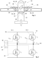
- Fig. 1 shows an aircraft 10 having at least one electrical consumer 12, at least one energy source 14 and at least one power electronic 16 for supplying the electrical consumer 12 with electrical power from the energy source 14.
- the power electronic 16 includes a semiconductor switch arrangement 18 and a control 20.
- the control 20 may be part of a component of the power electronic 16 or may be implemented as part of an outside control unit, e.g., in a computer unit 22 of the aircraft 10.
- the electrical consumer 12 can be of any kind of aircraft component to be powered with AC or DC power such as an electrical actor, a motor pump, or an electric motor 24.
- the motor 24 is a propulsion motor for driving a flight propulsion element such as a propeller 26 of the aircraft 10.
- the power electronic 16 or the semiconductor switch arrangement 18 is an inverter 28 for supplying the electrical consumer 12 with AC power converted from a DC energy source 14 such as a battery 30 or a fuel cell or a DC power network including several batteries and/or fuel cells (not shown).
- a DC energy source 14 such as a battery 30 or a fuel cell or a DC power network including several batteries and/or fuel cells (not shown).
- Other examples for the semiconductor switch arrangement 18 are DC/DC converters, AC/DC converters and power switches.
- Fig. 2 shows a simplified schematic diagram of an embodiment of the inverter 28 as an example for the power electronic 16 with the semiconductor switch arrangement 18.
- the semiconductor switch arrangement 18 includes a first semiconductor switch device 32.1 and a second semiconductor switch device 32.2 connected in parallel to each other between common nodes N1 and N2.
- the semiconductor switch devices 32.1, 32.2 are semiconductor power switches, especially single semiconductor power transistors such as field-effect transistors (FET), Mosfets or IGBTs.
- the semiconductor devices 32.1, 32.2 are modules including an arrangement of semiconductors to function as a power switch.
- the first and second semiconductor devices 32.1, 32.2 are MOSFETS.
- the inverter 28 includes a first to fourth transistor T1-T4 wherein two of them are connected in parallel to each other.
- an operation method for the semiconductor switch arrangement 18 enabling a paralleling of the semiconductor switch devices 32.1, 32.2 is explained in the following on basis of the first and second transistors T 1 , T 2 which are connected in parallel between the nodes N1 (e.g., power input for the first half of the inverter 28) and N2 (e.g., power output for outputting a load current I L to the load, e.g., one phase of the motor 24).
- the transistors T 1 , T 2 are Mosfets with Source, Drain and Gate.
- V GS1 designates the gate source voltage between gate and source of the first transistor T 1 (example for the first semiconductor switch device 32.1)
- V GS2 designates the gate-source voltage between gate and source of the second transistor T 2 (example for the second semiconductor switch device 32.2).
- i 1 represents the current through the first transistor T 1
- i 2 represents the current through the second transistor T 2
- I L represents the load current.
- Fig. 3 is a graph showing the course of the gate-source voltages V GS , V GS1 , V GS2 for the first and second transistors T 1 , T 2 and the course of the DC-link voltage V DS between drain and source, which corresponds to the voltage between the common nodes N1, N2, and of the currents I, i 1 , i 2 and I L over the time t.
- I L corresponds to the current I between the common nodes N1, N2.
- the gate source voltage V GS1 and the current i 1 for the first transistor T 1 is shown in broken lines, while the gate source voltage V GS2 and the current i 2 for the second transistor T 2 is shown in dotted lines.
- the control 20 may include a processor 34 and a computer readable medium, especially a memory 36, with a computer program containing instructions to carry out the following operation.
- the control routine may be part of a control for controlling the inverter 28 during different operation modes for driving the motor 24 or any other consumer 12.
- the control 20 controls the inverter 28 in the following way. For simplification only one phase with two paralleled switches - e.g., transistors T1, T2 - is shown.
- a first switching period SP1 at the beginning the first transistor T 1 is turned on and takes the full current I L .
- the second transistor T 2 is turned off a little bit earlier. Thus, the second transistor T 2 turns off at zero Voltage so that it has no losses. During this short time, the first transistor T 1 takes again the complete current and turns off.
- the time ts between turning on the one of the first and second transistors T1, T2 and then turning on the other of the first and second transistors T1, T2, is adjusted depending on measured parameters such as the temperature of the semiconductor switching device 32.1, 32.2.
- some embodiments comprise the steps of measuring at least one parameter indicative of a load or a loss in the first and/or second semiconductor switch 32.1, 32.2 (especially a device temperature) and adjusting, adapting or controlling the timing ts for turning the first and second semiconductor switch 32.1, 32.2 on and off depending on the at least one measured parameter.
- n transistors T 1 , T s ..., T n are connected in parallel between the common nodes N1, N2 for sharing the load.
- n switching periods SPn are conducted alternatively wherein in each of the n switching periods another one of the n transistors Tn is turned on first and turned off later while the other transistors are switched at zero Voltage.
- the invention provides an operation method for a semiconductor switch arrangement (18), especially of an aircraft (10) comprising a first semiconductor switch device (32.1) and a second semiconductor switch device (32.2) connected in parallel to each other between common nodes (N1, N2), the method comprising alternatively conducting a first switching period (SP1) and a second switching period (SP2), wherein the first switching period (SP1) comprises turning on the first switching device (32.1) to take the whole current (I L ) between the common nodes (N1, N2) first and then turning on the second switching device (32.2) at zero voltage between the common nodes (N1, N2), and wherein the second switching period (SP2) comprises turning on the second switching device (32.2) to take the whole current (I L ) between the common nodes first and then turning on the first switching device (32.1) at zero voltage between the common nodes (N1, N2).
- SP1 comprises turning on the first switching device (32.1) to take the whole current (I L ) between the common nodes (N1, N2) first and then turning on the second switching device (32.2) at
- a semiconductor switch arrangement (18) for an aircraft (10) comprising: a first semiconductor switch device (32.1) and a second semiconductor switch device (32.2) connected in parallel to each other between common nodes (N1, N2), and a control means (20) adapted to execute the steps of the aforementioned operation method.
Landscapes
- Engineering & Computer Science (AREA)
- Power Engineering (AREA)
- Inverter Devices (AREA)
Abstract
For enabling paralleling a low number of semiconductors or modules, especially for aircraft applications, in a simplified, reliable way with minimal additional effort, the invention provides an operation method for a semiconductor switch arrangement (18) comprising a first semiconductor switch device (32.1) and a second semiconductor switch device (32.2) connected in parallel to each other between common nodes (N1, N2), the method comprising alternatively conducting a first switching period (SP1) and a second switching period (SP2), wherein the first switching period (SP1) comprises turning on the first switching device (32.1) to take the whole current (IL) between the common nodes (N1, N2) first and then turning on the second switching device (32.2) at zero voltage between the common nodes (N1, N2), and wherein the second switching period (SP2) comprises turning on the second switching device (32.2) to take the whole current (IL) between the common nodes first and then turning on the first switching device (32.1) at zero voltage between the common nodes (N1, N2).
Description
- The invention relates to an operation method for a semiconductor switch arrangement comprising a first semiconductor switch device and a second semiconductor switch device connected in parallel to each other between common nodes, especially on an aircraft. Further, the invention provides to a semiconductor switch arrangement comprising a first semiconductor switch device and a second semiconductor switch device connected in parallel to each other between common nodes configured to be controlled in accordance with the operation method. Further, the invention provides an aircraft with such a semiconductor switch arrangement.
- For technical background, reference is made to the following literatures:
- [1] "Paralleling Power MOSFETs for Switching Applications", Semiconductor Components Industries, LLC, 2021, May, 2021 - Rev. 0,1 Publication Order Number: AND90108/D, download on 15.11.2023 under https://www.onsemi.com/pub/collateral/and90108-d.pdf
- [2] "Paralleling power MOSFETs in high current applications -Effect of MOSFET parameter mismatch on current and power dissipation imbalance", Edition 2021-05-14, AN_2009_PL18_2010_105641, Published by Infineon Technologies AG
- [3] Wikipedia "Power electronics" - download on 15.11.2023 from https://en.wikipedia.org/wiki/Power_electronics
- [4] "Hybrid and electric flight" - Airbus, download on 15.11.2023 from https://www.airbus.com/en/innovation/low-carbon-aviation/hybrid-and-electric-flight
- [5] Wikipedia - "Electric Aircraft" - download on 15.11.2023 from https://en.wikipedia.org/wiki/Electric_aircraft
- The invention relates to the field of power electronics, especially for aircraft, more preferably for electric aircrafts as referred to in [4] and [5]. More specifically, the invention relates to power electronics and optimized inverters, especially for an aircraft.
- Especially, the invention relates to semiconductor switch arrangements such as power switches, inverters, converters using paralleled semiconductor power switch devices such as power transistors, especially field-effect transistors (FETs), MOSFETS or IGBTs.
- Paralleling of semiconductor switch devices such as MOSFETs refers to the process of connecting multiple semiconductor switch devices such as MOSFETs in parallel to increase the overall current handling capacity of the circuit. This technique is commonly used in power electronics circuits - see [1] and [2] - to achieve high power output. When paralleling MOSFETs, it is important to ensure that each MOSFET is sharing the load equally to avoid any imbalance in current flow. One of the challenges of paralleling MOSFETs is ensuring that the MOSFETs share the current equally, especially in high-power applications. Advanced control techniques such as current sharing algorithms and dynamic load balancing have been developed to achieve this goal. These techniques use feedback control to adjust the gate voltage of each MOSFET to ensure that they share the current equally. These methods come with higher complexity and additional implementation effort. In state-of-the-art applications, paralleling of FETs is often done by creation of symmetrical layouts and using pre-selected components.
- An object of the invention is to enable paralleling a low number of semiconductors or modules, especially for aircraft applications, in a simplified, reliable way with minimal additional effort.
- For achieving such object, the invention provides the method and the arrangement of the enclosed independent claims.
- Advantageous embodiments are subject-matters of the dependent claims.
- The invention provides according to a one aspect thereof an operation method for a semiconductor switch arrangement comprising a first semiconductor switch device and a second semiconductor switch device connected in parallel to each other between common nodes, the method comprising alternatively conducting a first switching period and a second switching period,
wherein the first switching period comprises turning on the first switching device to take the whole current between the common nodes first and then turning on the second switching device at zero voltage between the common nodes, and wherein the second switching period comprises turning on the second switching device to take the whole current between the common nodes first and then turning on the first switching device at zero voltage between the common nodes. - Preferably, the first switching period further comprises turning off the second switching device first at zero voltage between the common nodes so that the first switching device takes the whole current between the common nodes and then turning off the first switching device and the second switching period further comprises turning off the first switching device first at zero voltage between the common nodes so that the second switching device takes the whole current between the common nodes and then turning off the second switching device.
- In some embodiments, the operation method is an operation method for operating a semiconductor switch arrangement comprising n semiconductor switch devices connected in parallel to each other between common nodes wherein n is a natural number with n>2, comprising alternatively conducting n switching periods wherein in each switching periods another of the n switching devices is turned on first to take the whole current between the common nodes and then the other of the n switching devices are turned on at zero voltage between the common nodes.
- In some embodiments, the timing between the turning on of the first and second switching devices - the first before the second or the second before the first - is chosen, adjusted or controlled dependent from additional measured data, especially including device temperature or power loss.
- In some embodiments, the semiconductor switch arrangement is one of the group consisting of a power switch, a power electronic, an inverter, a DC/DC converter, an AC/DC converter, a semiconductor switch arrangement for an aircraft, a semiconductor switch arrangement for an electrical power train of an aircraft, a power switch for an aircraft, a power electronic for an aircraft, an inverter for an aircraft, a DC/DC converter for an aircraft, an AC/DC converter for an aircraft.
- In some embodiments, each switching device is one from the group consisting of a power transistor, a field-effect-transistor, a MOSFET, an IGBT, and a semiconductor power switching module. All switching devices are of the same kind, e.g., a first and second MOSFET, or a first and second IGBT or a first and second module of equal design.
- Preferably, the operation method is conducted on an aircraft for providing an electrical consumer of the aircraft with electrical power. Especially, the method is an operation method for an inverter of an aircraft, such as a motor inverter for powering an electric motor of the aircraft, e.g., for propulsion.
- According to another aspect, the invention provides a semiconductor switch arrangement, especially for an aircraft, comprising:
- a first semiconductor switch device and a second semiconductor switch device connected in parallel to each other between common nodes, and
- a control means adapted to execute the steps of the operation method of any of the aforementioned embodiments.
- Preferably, the semiconductor switch arrangement is chosen from the group consisting of a power switch, a power electronic, an inverter, a DC/DC converter, an AC/DC converter, a semiconductor switch arrangement for an aircraft, a semiconductor switch arrangement for an electrical power train of an aircraft, a power switch for an aircraft, a power electronic for an aircraft, an inverter for an aircraft, a DC/DC converter for an aircraft, an AC/DC converter for an aircraft.
- Preferably, each switching device is chosen from the group consisting of a power transistor, a field-effect-transistor, a MOSFET, an IGBT, and a semiconductor power switching module. The same type is chosen for all paralleled semiconductor switch devices.
- According to another aspect, the invention provides a computer program comprising instructions to cause the semiconductor switch arrangement according to any of the aforementioned embodiments for the arrangement to execute the steps of the operation method of any of aforementioned embodiments for the operation method.
- According to another aspect, the invention provides an aircraft comprising a semiconductor switch arrangement according to of the aforementioned embodiments and/or a computer readable medium or memory having stored thereon the computer program as mentioned before.
- Preferred embodiments of the invention relate to paralleling of Mosfets or the like/ Modules by swapped switching control.
- Preferred embodiments of the invention describe a method to parallel a low number of semiconductors or modules in a simplified, reliable way with minimal additional effort.
- For an inverter using Power Mosfets, mainly switching losses and on-state losses determine the inverter behaviour and the achievable power ratings. Preferred embodiments of the invention mainly focuse on the switching losses.
- As indicated in [1] and [2], when paralleling multiple semiconductors, it is up to now important that all devices exactly switch identically to share the losses equally. Unfortunately, semiconductors never behave the same (as e.g., the threshold voltage differs slightly between devices). This means one semiconductor switches earlier and therefore takes more losses. This leads to an unbalanced load sharing if no countermeasure is taken.
- To overcome this, the invention proposes an inconvenient way of controlling the semiconductors during switching.
- As equal switching never can be achieved by 100% (only when one single semiconductor is switching) preferred embodiments of the invention control the inverter or the like in a way where only one semiconductor switch is switching at each transition.
- Assuming that more than one semiconductor switch is put in parallel, the switching one takes the complete current and therefore generates additional losses. Within the next period the second semiconductor switch (e.g., transistor) turns on earlier and therefore takes all the switching losses. The semiconductor switch turning on later always switches at zero voltage and therefore switches without any losses (zero voltage switching).
- By swapping all paralleled semiconductor switches (e.g., transistors), an equal averaging can be achieved. Due to that mechanism, differences in switching behaviour are equalled out and losses across the paralleled switching devices (e.g., transistors; FETs, MOSFETs,) are averaged.
- The efficiency of this method can even be increased by adjusting the timings when the dedicated semiconductors turn on or off.
- Preferred embodiments of the invention offer a very simple method to control paralleled semiconductors or modules without the need of complex control algorithms. In case of additional available measurement data (e.g., device temperature) the proposed solution can be optimized by a smarter timing.
- A smarter timing also allows to compensate for differences in the on-state behaviour as the current conduction time of the single devices can be controlled in a flexible manner.
- If multiple (more than 2) devices are used it is implicitly foreseen that the active switching transistor can withstand the overall phase current of one single phase (only for a very short time).
- Preferred embodiments of the invention have one, several or all of the following advantages:
- Due to the simplicity of the concept, the system works very reliable.
- Low control effort is necessary
- Preselection of components can be relaxed
- Preferred uses of embodiments of the invention are power electronic systems for providing an aircraft component, especially a drive train, with electrical power. For example, embodiments of the invention are used in inverters for powering an electric motor with energy from a DC energy source such as a battery or a fuel cell.
- Embodiments of the invention are explained below referring to the accompanying drawings in which:
- Fig. 1
- is a schematic plan view of an embodiment of an aircraft with a semiconductor switching arrangement such as an inverter of an electric drive;
- Fig. 2
- a simplified diagram of an embodiment of an inverter as example for the semiconductor switching arrangement with a plurality of semiconductor switch devices connected in parallel between common nodes;
- Fig. 3
- a graph with timings of control voltages for the semiconductor switching devices and of voltages and currents between the common nodes for illustrating an operation method for the semiconductor switching arrangement.
-
Fig. 1 shows anaircraft 10 having at least oneelectrical consumer 12, at least oneenergy source 14 and at least one power electronic 16 for supplying theelectrical consumer 12 with electrical power from theenergy source 14. The power electronic 16 includes asemiconductor switch arrangement 18 and acontrol 20. - The
control 20 may be part of a component of the power electronic 16 or may be implemented as part of an outside control unit, e.g., in acomputer unit 22 of theaircraft 10. - The
electrical consumer 12 can be of any kind of aircraft component to be powered with AC or DC power such as an electrical actor, a motor pump, or anelectric motor 24. For example, themotor 24 is a propulsion motor for driving a flight propulsion element such as apropeller 26 of theaircraft 10. - In some embodiments, the power electronic 16 or the
semiconductor switch arrangement 18 is aninverter 28 for supplying theelectrical consumer 12 with AC power converted from aDC energy source 14 such as abattery 30 or a fuel cell or a DC power network including several batteries and/or fuel cells (not shown). Other examples for thesemiconductor switch arrangement 18 are DC/DC converters, AC/DC converters and power switches. -
Fig. 2 shows a simplified schematic diagram of an embodiment of theinverter 28 as an example for the power electronic 16 with thesemiconductor switch arrangement 18. As shown in the example ofFig. 2 , thesemiconductor switch arrangement 18 includes a first semiconductor switch device 32.1 and a second semiconductor switch device 32.2 connected in parallel to each other between common nodes N1 and N2. - In some embodiments, the semiconductor switch devices 32.1, 32.2 are semiconductor power switches, especially single semiconductor power transistors such as field-effect transistors (FET), Mosfets or IGBTs. In other embodiments (not shown), the semiconductor devices 32.1, 32.2 are modules including an arrangement of semiconductors to function as a power switch. In the embodiment shown, the first and second semiconductor devices 32.1, 32.2 are MOSFETS. Especially, the
inverter 28 includes a first to fourth transistor T1-T4 wherein two of them are connected in parallel to each other. - Referring to
Figs. 2 and3 , an operation method for thesemiconductor switch arrangement 18 enabling a paralleling of the semiconductor switch devices 32.1, 32.2 is explained in the following on basis of the first and second transistors T1, T2 which are connected in parallel between the nodes N1 (e.g., power input for the first half of the inverter 28) and N2 (e.g., power output for outputting a load current IL to the load, e.g., one phase of the motor 24). The transistors T1, T2 are Mosfets with Source, Drain and Gate. VGS1 designates the gate source voltage between gate and source of the first transistor T1 (example for the first semiconductor switch device 32.1), VGS2 designates the gate-source voltage between gate and source of the second transistor T2 (example for the second semiconductor switch device 32.2). i1 represents the current through the first transistor T1, i2 represents the current through the second transistor T2, and IL represents the load current. -
Fig. 3 is a graph showing the course of the gate-source voltages VGS, VGS1, VGS2 for the first and second transistors T1, T2 and the course of the DC-link voltage VDS between drain and source, which corresponds to the voltage between the common nodes N1, N2, and of the currents I, i1, i2 and IL over the time t. IL corresponds to the current I between the common nodes N1, N2. The gate source voltage VGS1 and the current i1 for the first transistor T1 is shown in broken lines, while the gate source voltage VGS2 and the current i2 for the second transistor T2 is shown in dotted lines. - The
control 20 may include aprocessor 34 and a computer readable medium, especially amemory 36, with a computer program containing instructions to carry out the following operation. The control routine may be part of a control for controlling theinverter 28 during different operation modes for driving themotor 24 or anyother consumer 12. - The
control 20 controls theinverter 28 in the following way. For simplification only one phase with two paralleled switches - e.g., transistors T1, T2 - is shown. - In a first switching period SP1, at the beginning the first transistor T1 is turned on and takes the full current IL.
- When the current commutation is done (VDS = 0V), T2 also turns on. This leads to the situation that the load current IL is equally shared between the first and second transistors T1 andT2.
- The second transistor T2 is turned off a little bit earlier. Thus, the second transistor T2 turns off at zero Voltage so that it has no losses. During this short time, the first transistor T1 takes again the complete current and turns off.
- In the next period - second switching period SP2 -, the procedure is repeated but with the second transistor T2 turning on earlier and off later.
- After that the first period SP1 is conducted again.
- In some embodiments, the time ts between turning on the one of the first and second transistors T1, T2 and then turning on the other of the first and second transistors T1, T2, is adjusted depending on measured parameters such as the temperature of the semiconductor switching device 32.1, 32.2.
- Thus, some embodiments comprise the steps of measuring at least one parameter indicative of a load or a loss in the first and/or second semiconductor switch 32.1, 32.2 (especially a device temperature) and adjusting, adapting or controlling the timing ts for turning the first and second semiconductor switch 32.1, 32.2 on and off depending on the at least one measured parameter.
- In further embodiments (not shown), n transistors T1, Ts..., Tn are connected in parallel between the common nodes N1, N2 for sharing the load. In this case n switching periods SPn are conducted alternatively wherein in each of the n switching periods another one of the n transistors Tn is turned on first and turned off later while the other transistors are switched at zero Voltage.
- By swapping all paralleled semiconductor switches 32.1, 32.2, 32.n (e.g., transistors T1, T2, Tn), an equal averaging can be achieved. Due to that mechanism, differences in switching behaviour are equalled out and losses across the paralleled switching devices 32.1, 32.2 are averaged.
- For enabling paralleling a low number of semiconductors or modules, especially for aircraft applications, in a simplified, reliable way with minimal additional effort, the invention provides an operation method for a semiconductor switch arrangement (18), especially of an aircraft (10) comprising a first semiconductor switch device (32.1) and a second semiconductor switch device (32.2) connected in parallel to each other between common nodes (N1, N2), the method comprising alternatively conducting a first switching period (SP1) and a second switching period (SP2), wherein the first switching period (SP1) comprises turning on the first switching device (32.1) to take the whole current (IL) between the common nodes (N1, N2) first and then turning on the second switching device (32.2) at zero voltage between the common nodes (N1, N2), and wherein the second switching period (SP2) comprises turning on the second switching device (32.2) to take the whole current (IL) between the common nodes first and then turning on the first switching device (32.1) at zero voltage between the common nodes (N1, N2).
- Further, a semiconductor switch arrangement (18) for an aircraft (10) has been described, comprising:
a first semiconductor switch device (32.1) and a second semiconductor switch device (32.2) connected in parallel to each other between common nodes (N1, N2), and a control means (20) adapted to execute the steps of the aforementioned operation method. -
- 10
- aircraft
- 12
- electrical consumer
- 14
- energy source
- 16
- power electronic
- 18
- semiconductor switch arrangement
- 20
- control
- 22
- computer unit
- 24
- motor
- 26
- propeller
- 28
- inverter
- 30
- battery
- 32.1
- first semiconductor switch
- 32.2
- second semiconductor switch
- 34
- processor
- 36
- memory
- i1
- source drain current through first transistor
- i2
- source drain current through second transistor
- IL
- load current
- N1
- first node
- N2
- second node
- T1
- first transistor (example for first semiconductor switching device)
- T2
- second transistor (example for second semiconductor device)
- T3
- third transistor
- T4
- fourth transistor
- VDC
- DC link voltage
- VDS
- drain source voltage (voltage between common nodes)
- VGS1
- gate source voltage (first transistor)
- VGS2
- gate source voltage (second transistor)
Claims (11)
- Operation method for a semiconductor switch arrangement (18) comprising a first semiconductor switch device (32.1) and a second semiconductor switch device (32.2) connected in parallel to each other between common nodes (N1, N2), the method comprising alternatively conducting a first switching period (SP1) and a second switching period (SP2),wherein the first switching period (SP1) comprises turning on the first switching device (32.1) to take the whole current (IL) between the common nodes (N1, N2) first and then turning on the second switching device (32.2) at zero voltage between the common nodes (N1, N2), andwherein the second switching period (SP2) comprises turning on the second switching device (32.2) to take the whole current (IL) between the common nodes first and then turning on the first switching device (32.1) at zero voltage between the common nodes (N1, N2).
- Operation method according to claim 1 whereinthe first switching period (SP1) further comprises turning off the second switching device (32.2) first at zero voltage between the common nodes (N1, N2) so that the first semiconductor switching device (32.1) takes the whole current (IL) between the common nodes (N1, N2) and then turning off the first switching device (32.1) andthe second switching period (SP2) further comprises turning off the first switching device (32.1) first at zero voltage between the common nodes (N1, N2) so that the second semiconductor switching device (32.2) takes the whole current (IL) between the common nodes (N1, N2) and then turning off the second switching device (32.2).
- Operation method according to any of the preceding claims for a semiconductor switch arrangement (18) comprising n semiconductor switch devices (32.1, 32.2,..) connected in parallel to each other between common nodes (N1, N2) wherein n is a natural number with n>2, comprising alternatively conducting n switching periods wherein in each of the n switching period another of the n semiconductor switching devices is turned on first to take the whole current (IL) between the common nodes (N1, N2) and then the other of the n semiconductor switching devices are turned on at zero voltage between the common nodes (N1, N2).
- Operation method according to any of the preceding claims wherein the timing (ts) between the turning on of the first and second switching devices (32.1, 32.2) is chosen, adjusted or controlled dependent from additional measured data, especially including device temperature or power loss.
- Operation method according to any of the preceding claims wherein5.1 the semiconductor switch arrangement (18) is one of the group consisting of a power switch, a power electronic (16), an inverter (28), a DC/DC converter, a AC/DC converter, a semiconductor switch arrangement (18) for an aircraft (10), a semiconductor switch arrangement (18) for an electrical power train of an aircraft (10), a power switch for an aircraft, a power electronic (16) for an aircraft (10), an inverter (28) for an aircraft (10), a DC/DC converter for an aircraft, a AC/DC converter for an aircraft; and/or5.2 each semiconductor switching device is one from the group consisting of a power transistor (T1-T4), a field-effect-transistor, a MOSFET, an IGBT, and a semiconductor power switching module.
- Operation method according to any of the preceding claims, wherein the operation method is conducted on an aircraft (10) for providing an electrical consumer (12) of the aircraft (10) with electrical power.
- Semiconductor switch arrangement (18) comprising:a first semiconductor switch device (32.1) and a second semiconductor switch device (32.2) connected in parallel to each other between common nodes (N1, N2), anda control means (20) adapted to execute the steps of the operation method of any of the proceeding claims.
- Semiconductor switch arrangement (18) according to claim 7, chosen from the group consisting of a power switch, a power electronic (16), an inverter (28), a DC/DC converter, a AC/DC converter, a semiconductor switch arrangement (18) for an aircraft (10), a semiconductor switch arrangement (18) for an electrical power train of an aircraft (10), a power switch for an aircraft, a power electronic (16) for an aircraft (10), an inverter (28) for an aircraft (10), a DC/DC converter for an aircraft (10), a AC/DC converter for an aircraft (10).
- Semiconductor switch arrangement (18) according to any of the claims 7 and 8, wherein each semiconductor switching device (32.1, 32.2) is one from the group consisting of a power transistor (T1-T4), a field-effect-transistor, a MOSFET, an IGBT, and a semiconductor power switching module.
- Computer program comprising instructions to cause the semiconductor switch arrangement (18) according to any of the claims 7 to 9 to execute the steps of the operation method of any of the claims 1 to 6.
- Aircraft (10) comprising a semiconductor switch arrangement (18) according to any of the claims 7 to 9 and/or a computer readable medium or memory (36) having stored thereon the computer program of claim 10.
Priority Applications (1)
| Application Number | Priority Date | Filing Date | Title |
|---|---|---|---|
| EP23213100.3A EP4564675A1 (en) | 2023-11-29 | 2023-11-29 | Paralleling semiconductor switch devices, especially in an aircraft |
Applications Claiming Priority (1)
| Application Number | Priority Date | Filing Date | Title |
|---|---|---|---|
| EP23213100.3A EP4564675A1 (en) | 2023-11-29 | 2023-11-29 | Paralleling semiconductor switch devices, especially in an aircraft |
Publications (1)
| Publication Number | Publication Date |
|---|---|
| EP4564675A1 true EP4564675A1 (en) | 2025-06-04 |
Family
ID=89030051
Family Applications (1)
| Application Number | Title | Priority Date | Filing Date |
|---|---|---|---|
| EP23213100.3A Withdrawn EP4564675A1 (en) | 2023-11-29 | 2023-11-29 | Paralleling semiconductor switch devices, especially in an aircraft |
Country Status (1)
| Country | Link |
|---|---|
| EP (1) | EP4564675A1 (en) |
Citations (5)
| Publication number | Priority date | Publication date | Assignee | Title |
|---|---|---|---|---|
| JPS5465351A (en) * | 1977-11-01 | 1979-05-25 | Toshiba Corp | Parallel operating system of switching elements |
| US5399908A (en) * | 1992-06-26 | 1995-03-21 | Kollmorgen Corporation | Apparatus and method for forced sharing of parallel MOSFET switching losses |
| US20160218621A1 (en) * | 2015-01-22 | 2016-07-28 | Denso Corporation | Controller for power converter |
| KR102403150B1 (en) * | 2020-10-21 | 2022-05-27 | 경북대학교 산학협력단 | Apparatus for semiconductor switch |
| EP4064564A1 (en) * | 2021-03-24 | 2022-09-28 | Siemens Gamesa Renewable Energy Innovation & Technology S.L. | Control method of a hybrid power switch |
-
2023
- 2023-11-29 EP EP23213100.3A patent/EP4564675A1/en not_active Withdrawn
Patent Citations (5)
| Publication number | Priority date | Publication date | Assignee | Title |
|---|---|---|---|---|
| JPS5465351A (en) * | 1977-11-01 | 1979-05-25 | Toshiba Corp | Parallel operating system of switching elements |
| US5399908A (en) * | 1992-06-26 | 1995-03-21 | Kollmorgen Corporation | Apparatus and method for forced sharing of parallel MOSFET switching losses |
| US20160218621A1 (en) * | 2015-01-22 | 2016-07-28 | Denso Corporation | Controller for power converter |
| KR102403150B1 (en) * | 2020-10-21 | 2022-05-27 | 경북대학교 산학협력단 | Apparatus for semiconductor switch |
| EP4064564A1 (en) * | 2021-03-24 | 2022-09-28 | Siemens Gamesa Renewable Energy Innovation & Technology S.L. | Control method of a hybrid power switch |
Non-Patent Citations (5)
| Title |
|---|
| "Edition", INFINEON TECHNOLOGIES AG, article "Paralleling power MOSFETs in high current applications -Effect of MOSFET parameter mismatch on current and power dissipation imbalance" |
| "Hybrid and electric flight", AIRBUS, 15 November 2023 (2023-11-15), Retrieved from the Internet <URL:https://www.airbus.com/en/innovation/low-carbon-aviation/hybrid-and-electric-flight> |
| "Semiconductor Components Industries", May 2021, LLC, article "Paralleling Power MOSFETs for Switching Applications" |
| WIKIPEDIA, ELECTRIC AIRCRAFT, 15 November 2023 (2023-11-15) |
| WIKIPEDIA, POWER ELECTRONICS, 15 November 2023 (2023-11-15), Retrieved from the Internet <URL:https://en.wikipedia.org/wiki/Power_electronics> |
Similar Documents
| Publication | Publication Date | Title |
|---|---|---|
| CN111384718A (en) | Power supply device, power supply system and data center | |
| RU2669760C1 (en) | Power supply system for electric vehicles | |
| CN105846403B (en) | DC power system | |
| CN105658467A (en) | Power conversion device and power conversion method | |
| US7061134B2 (en) | Method and system for improved thermal management of a voltage source inverter operating at low output frequency utilizing a zero vector modulation technique | |
| US20250202384A1 (en) | Power conversion device and flying object | |
| EP3633843B1 (en) | Current converter and driving method therefor | |
| WO2021175204A1 (en) | Three-level active neutral-point-clamped converter and operating method therefor and control device | |
| CN113346730B (en) | Power factor correction circuit and operation method of uninterruptible power supply device | |
| US9484837B2 (en) | Switching branch for three-level inverter and method for controlling switching branch of three-level inverter | |
| US10056837B2 (en) | DC-DC converter and power source device | |
| US10917000B2 (en) | Driver unit, electric power converter, vehicle and method for operating an electric power converter | |
| CN115940654B (en) | A power supply and computing device | |
| CN107852097A (en) | For controlling the DC DC converters and its corresponding control methods and blower fan of aircraft blower fan inverter | |
| KR100814349B1 (en) | Open- and closed-loop control methods and devices | |
| EP3565095A1 (en) | Reduced power dissipation power converter configuration | |
| US10770962B2 (en) | Converter cell comprising an energy converter in parallel to a clamp inductor | |
| US11822404B2 (en) | Power distribution system and server system | |
| US20260106565A1 (en) | Hybrid conversion device including switching modules for different switch compositions | |
| JP6739865B2 (en) | Semiconductor device | |
| US20240176377A1 (en) | Method for operating a gate driver system for a multi-level converter system, data processing apparatus, computer program, computer readable storage medium, gate driver system, multi-level converter system, and vehicle | |
| EP4203288A1 (en) | Active dc bus voltage balancing circuit | |
| US10848049B2 (en) | Main conversion circuit, power conversion device, and moving body | |
| EP3086458B1 (en) | Inverter circuit and method for producing inverter circuit | |
| RU2757695C2 (en) | Control of the number of active power elements of the speed controller |
Legal Events
| Date | Code | Title | Description |
|---|---|---|---|
| PUAI | Public reference made under article 153(3) epc to a published international application that has entered the european phase |
Free format text: ORIGINAL CODE: 0009012 |
|
| STAA | Information on the status of an ep patent application or granted ep patent |
Free format text: STATUS: THE APPLICATION HAS BEEN PUBLISHED |
|
| AK | Designated contracting states |
Kind code of ref document: A1 Designated state(s): AL AT BE BG CH CY CZ DE DK EE ES FI FR GB GR HR HU IE IS IT LI LT LU LV MC ME MK MT NL NO PL PT RO RS SE SI SK SM TR |
|
| STAA | Information on the status of an ep patent application or granted ep patent |
Free format text: STATUS: THE APPLICATION IS DEEMED TO BE WITHDRAWN |
|
| 18D | Application deemed to be withdrawn |
Effective date: 20251205 |