EP4564608A1 - Frequency selective surface - Google Patents
Frequency selective surface Download PDFInfo
- Publication number
- EP4564608A1 EP4564608A1 EP23856350.6A EP23856350A EP4564608A1 EP 4564608 A1 EP4564608 A1 EP 4564608A1 EP 23856350 A EP23856350 A EP 23856350A EP 4564608 A1 EP4564608 A1 EP 4564608A1
- Authority
- EP
- European Patent Office
- Prior art keywords
- metal
- stub
- bandpass
- frequency selective
- selective surface
- Prior art date
- Legal status (The legal status is an assumption and is not a legal conclusion. Google has not performed a legal analysis and makes no representation as to the accuracy of the status listed.)
- Pending
Links
Images


Classifications
-
- H—ELECTRICITY
- H01—ELECTRIC ELEMENTS
- H01Q—ANTENNAS, i.e. RADIO AERIALS
- H01Q15/00—Devices for reflection, refraction, diffraction or polarisation of waves radiated from an antenna, e.g. quasi-optical devices
- H01Q15/0006—Devices acting selectively as reflecting surface, as diffracting or as refracting device, e.g. frequency filtering or angular spatial filtering devices
- H01Q15/0013—Devices acting selectively as reflecting surface, as diffracting or as refracting device, e.g. frequency filtering or angular spatial filtering devices said selective devices working as frequency-selective reflecting surfaces, e.g. FSS, dichroic plates, surfaces being partly transmissive and reflective
Definitions
- Examples of the present disclosure relate to the field of communications, and in particular, to a frequency selective surface.
- Frequency selective surface is an artificial electromagnetic material having a special filtering function, and is widely applied in fields such as radar, aviation, and communications.
- multi-band integration is an important direction, and an antenna with an electromagnetic opening characteristic gradually emphasizes a problem of mutual interference between frequency bands in the multi-band integration, and research on a multi-band FSS has become a great emphasis.
- the multi-band FSS often uses a multi-layer cascaded FSS technology, or a multi-resonant stub technology.
- the multi-layer cascaded FSS increases the complexity and cost of design and fabrication, and is greatly limited in the civil field.
- the multi-resonant stub technology refers to integrating multiple stubs within a single FSS unit, and generating passbands of multiple frequency bands by means of resonance of the multiple stubs. The issue with this technique is that when the wavelength of a second passband is much smaller than that of the first passband, the filtering performance of the FSS structure in the second passband is difficult to ensure, since the size of the FSS unit is always determined by the first passband.
- the examples of the present disclosure provide a frequency selective surface, so as to at least solve the problems in the related art that the single-layer FSS can support fewer passbands and the wide-angle filtering performance is poor.
- a frequency selective surface unit including at least one first bandpass stub, wherein the two first metal patches are spaced apart to form a first capacitor of physical width L, L is a positive number, the first metal wire is connected to the two first metal patches to form a first inductor, wherein connection positions of the first metal wire and the two first metal patches are both located within the range of L/4 to 3L/4 of the physical width L of the first capacitor; and a dielectric substrate, for fixing the first bandpass stub.
- a frequency selective surface is further provided, which includes multiple frequency selective surface units as described above.
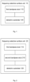
- a frequency selective surface unit including a first bandpass stub 110 and a dielectric substrate 120 for fixing the first bandpass stub 110, the first bandpass stub 110 includes two first metal patches and a first metal wire, wherein the two first metal patches are spaced apart to form a first capacitor having a physical width of L, L is a positive number, a first metal wire is connected to two first metal patches to form a first inductor, and the connection position of the first metal wire and the two first metal patches is located at L/4 to 3L/4 of the physical width L of the first capacitor, the problems in the related art that the single-layer FSS can support fewer passbands and the wide-angle filtering performance is poor are solved, and the effect of improving the FSS filtering performance is achieved.
- the manner of fixing the first bandpass stub 110 on the dielectric substrate 120 includes: two first metal patches being fixed on the same side of the dielectric substrate; or the two first metal patches are respectively fixed on opposite sides of the dielectric substrate, and the first metal wires are fixed on the opposite sides of the dielectric substrate and are connected through the metallized via.
- the first metal wire may comprise multiple metal segments fixed on the opposite sides of the dielectric substrate, and the multiple metal segments are connected through multiple metallized vias.
- the shape of the first metal patch may be circular, triangular, rectangular, or irregular polygonal.
- figure 2 is a block diagram of a frequency selective surface unit according to an embodiment of the present disclosure, as shown in figure 2 , the frequency selective surface unit 20 further includes a second bandpass stub 210 in addition to the components in figure 1 , the second bandpass stub 210 and the first bandpass stub 110 can be connected through a metal wire, and the second bandpass stub 210 includes two second metal patches and a second metal wire.
- the two second metal patches may be distributed on opposite sides of the dielectric substrate 120 to form the second capacitor
- the second metal wires may be distributed on the opposite sides of the dielectric substrate 120 and connected through the metalized vias to form the second inductor
- the second inductor and the second capacitor are connected in parallel.
- the second metal wire may comprise multiple metal segments fixed on the opposite sides of the dielectric substrate, and the multiple metal segments are connected through multiple metallized vias.
- the shape of the second metal patch may be circular, triangular, rectangular, or irregular polygonal.
- figure 3 is a block diagram of a frequency selective surface unit according to an embodiment of the present disclosure, as shown in figure 3 , in addition to the components in figure 2 , the frequency selective surface unit 30 further includes at least one first bandstop stub 310, the first bandstop stub 310 is connected to the first bandpass stub 110 via a metal wire, and the first bandstop stub 310 includes two third metal patches and a third metal wire.
- the two third metal patches may be distributed on opposite sides of the dielectric substrate 120 to form a third capacitor, and the third metal wire is configured to connect the second bandpass stub 210 and the first bandpass stub 110 to form a third inductor.
- the shape of the third metal patch may be circular, triangular, rectangular, or irregular polygonal.
- a frequency selective surface including multiple the above frequency selective surface units.
- two adjacent frequency selective surface units share two third metal patches, so that two adjacent frequency selective surface units share a third capacitor.
- a third capacitance of the first bandpass stub is shared between adjacent frequency selective surface units in diagonally opposing corner locations of the frequency selective surface.
- the FSS unit has the characteristics of a low-cost and miniaturized single layer with stable multi-band and 60-degree wide-angle performance, and can solve the problems in the prior art that the single-layer FSS can support fewer passbands, the wide-angle filtering performance is poor, and the cost of a multi-layer FSS is high.
- FIG. 4 is a structural block diagram of an FSS unit according to an example of the present disclosure.
- the FSS unit structure includes a first bandpass stub 100, a second bandpass stub 200, a first bandstop stub 300, and three stubs being composed of a metal structure and partial metallized vias which are located on opposite sides of a dielectric substrate, three stubs are connected through a metal wire, each stub respectively corresponds to a different passband/stopband, and electromagnetic waves of a passband frequency band can pass through the FSS structure, thereby achieving transmission; The electromagnetic wave of the stopband frequency band cannot pass through the FSS structure, thereby implementing reflection.
- FIG. 5 is a schematic structural diagram of a first bandpass stub according to a scenario embodiment of the present disclosure.
- the first bandpass stub 100 includes a first metal structure 101, a second metal structure 102, and a third metal structure 103, where the first metal structure 101 and the second metal structure 102 have a certain distance therebetween to form a capacitor, and the physical width of the capacitor is L;
- the third metal structure 103 is a metal wire, so as to form an inductor, in which the narrower the metal wire is, the higher the inductance value is;
- the positions of connections between the inductor and the capacitor are respectively a first connection position 104 and a second connection position 105, in which the first connection position 104 and the second connection position 105 can move in a range of (L/4,3L/4), and when 104 and 105 are located at the central L/2 position in the width direction, a better resonance characteristic can be obtained.
- first metal structure 101 and the second metal structure 102 of the first bandpass stub are the first metal patches in the foregoing embodiment, and the first metal structure 101 and the second metal structure 102 may be in the same layer, or may be in different layers of the dielectric substrate, and may be in various shapes such as rectangle, triangle, and circle.
- the third metal structure 103 is the first metal wire in the foregoing embodiment, and the third metal structure 103 may be in one layer, and may also be multiple segments of metal wires distributed on the opposite sides of the dielectric substrate, and are connected through metal vias.
- a first connection location 104 and a second connection location 105 of the inductor and capacitor connection structure which may be a direct connection of a metal structure, and may also be a connection of a metallized via; the linkage position range was also (L/4,3L/4).
- the first bandpass stub adopts a wide-angle design, i.e. a position where an inductor is connected to a capacitor in parallel; and in the centre of the width L of the capacitor, the position thereof can be adjusted in a range from L/4 to 3L/4.
- FIG. 6 is a schematic structural diagram of a second bandpass stub according to a scenario embodiment of the present disclosure.
- the second bandpass stub 200 includes a fourth metal structure 201 and a fifth metal structure 202 on the front side of the dielectric substrate, a sixth metal structure 203 and a seventh metal structure 204 on the back side of the dielectric substrate, and a metallized via 205 connecting the front side and the back side of the dielectric substrate.
- the fourth metal structure 201 and the sixth metal structure 203 are respectively located on opposite sides of the dielectric substrate to form a plate capacitor, and in a direction perpendicular to the dielectric substrate, the more projected overlapping portions of the fourth metal structure 201 and the sixth metal structure 203 are, the larger the capacitor is; the fifth metal structure 202 and the seventh metal structure 204 are connected through a metallized via 205 to form an inductor.
- the fifth metal structure 202 and the seventh metal structure 204 may be metal wires, and the narrower the metal wire is, the higher the inductance value is; the capacitor and the inductor are connected in parallel.
- the second bandpass stub forms a capacitor by means of metal structures distributed on two surfaces of a substrate, and compared with a capacitor structure located on the same side, a gap between metal structures on the same side is replaced by a distance of the thickness of the substrate, thereby reducing the length of the stub on the same plane, and realizing miniaturization.
- the fourth metal structure 201 and the sixth metal structure 203 in the second bandpass stub are the second metal patch in the above example, and the fourth metal structure 201 and the sixth metal structure 203 may be rectangular, or may be circular, triangular, polygonal or other non-standard shapes.
- the fifth metal structure 202 and the seventh metal structure 204 are the second metal wires in the foregoing embodiment, and the fifth metal structure 202 and the seventh metal structure 204 may be two-segment metal wires, or may be multi-segment metal wires, and are connected through multiple metallization vias.
- the second bandpass stub uses a miniaturized design, and a metal structure respectively located on the opposite sides of a plate forms a capacitor, metal wires extending out from the opposite sides of the metal structure are connected through a metalized via to form an inductor, and the capacitor and the inductor are connected in parallel to form a second pass-band.
- Figure 7 is a schematic structural diagram of a first bandstop stub according to a scenario embodiment of the present disclosure.
- the first bandstop stub 300 includes an eighth metal structure 301, a ninth metal structure 302, and a twelfth metal structure 305 on a front side of a dielectric substrate, a tenth metal structure 303, an eleventh metal structure 304, and a thirteenth metal structure 306 on a back side of the dielectric substrate.
- the eighth metal structure 301, the eleventh metal structure 304, the twelfth metal structure 305, and the thirteenth metal structure 306 are metal connecting wires between the stubs, and form an inductor together with other stubs.
- the opposite sides of the dielectric substrate of the first bandstop stub, the ninth metal structure 302 and the tenth metal structure 303 are the third metal patches in the foregoing embodiment, and the ninth metal structure 302 and the tenth metal structure 303 may be circular, may also be triangular, rectangular, polygonal, or other irregular shapes.
- the first bandstop stub is of a miniaturized design, and a capacitor is formed by metal structures located on opposite sides of a plate, wherein the front and back metal structures respectively belong to two adjacent units in positive and negative 45 directions.
- a single unit capacitor is 2C
- two capacitors of adjacent units are in a series connection relationship, so that an actual capacitance value is halved to C.
- a capacitance value equivalent to the unit capacitor C is C.
- a required capacitance value is reduced, that is, the area of a capacitor metal is reduced, thereby realizing the miniaturization of bandstop stubs.
- the metal structure mentioned in this scenario embodiment may be a metal patch, a metal strip, a metal line, and the like, which is not limited herein.
- the FSS provided in this scenario embodiment is an FSS minimum repeatable sub-array, and the sub-array includes four basic units with consistent functions.
- Each base unit includes a first bandpass stub, a second bandpass stub, and a first bandstop stub.
- Adjacent basic units at diagonal positions share the capacitance of the first bandstop stub 300, and therefore, the same-function stubs of adjacent basic units are respectively located on opposite sides of the dielectric substrate, that is, assuming that the first bandpass stub of one basic unit is located on the front side of the dielectric substrate, the first bandpass stub of one diagonal adjacent basic unit is located on the back side of the dielectric substrate.
- the size of the miniaturized FSS unit is 20 mm, which is equivalent to 0.17 ⁇ @2.6 GHz and 0.23 ⁇ @3.5 GHz.
- an electromagnetic wave of a bandstop frequency band is incident on a surface of an FSS
- a first bandstop stub generates LC series resonance, which is equivalent to the metal transmission line
- the FSS is equivalent to the metal grid, so as to block the propagation of the electromagnetic wave and reflect same.
- the first or second bandpass stub When electromagnetic waves of a cut-off frequency band are incident on the surface of an FSS, the first or second bandpass stub generates LC parallel resonance to form a high-impedance metal transmission line, the FSS cannot form a metal grid, and the electromagnetic waves pass through the FSS to form transmission.
- Figure 8 is a graph of a transmission-coefficient curve of an FSS according to a scenario embodiment of the present disclosure. As shown in figure 8 , it can be seen that the FSS proposed in the second embodiment of the scenario realizes a bandstop function with a transmission coefficient of less than -15 dB in a frequency band of 0.6 GHz-0.96 GHz; in addition, the transmission-coefficient of two frequency bands, i.e.
- 2.5 GHz-2.7 GHz and 3.4 GHz-3.8 GHz is greater than -0.5 dB, thereby realizing a dual-frequency bandpass function; when the light is incident at a wide angle of 60 degrees, in a conventional structure, in a first transparent frequency band, the transmission loss sharply increases, and by adopting the miniaturized wide-angle unit of the present disclosure, the loss is greatly improved.
- the structural form of a relevant stub (including a first bandpass stub, a second bandpass stub, and a first bandstop stub) is not specifically limited, and can be adjusted according to actual situations.
- the structure of the first relay node may be located on the opposite sides of the dielectric substrate.
- Figure 9 is a structural block diagram of a first bandpass stub according to a scenario embodiment of the present disclosure.
- the first connection terminal includes a fourteenth metal structure 111 and a fifteenth metal structure 112, which are respectively located on opposite sides of a dielectric substrate to form a capacitor, the overall width of the capacitor being L; the first metal wire 113 and the second metal wire 115 are respectively located on opposite sides of the dielectric substrate, and are connected to form an inductor through a metallized via 114; a first inductive loading position 116 and a second inductive loading position 117, which are connected to a capacitor through a metalized via, in which the range of loading positions is (L/4, 3L/4).
- FIG. 10 is a structural block diagram of a first bandpass stub according to a scenario embodiment of the present disclosure.
- the first bandpass stub includes a sixteenth metal structure 121 and a seventeenth metal structure 122, which are located on opposite sides of a dielectric substrate respectively to form a capacitor, the overall width of the capacitor being L; the third metal wire 123 forms an inductor; a third inductor loading position 124 and a fourth inductor loading position 125, wherein the third inductor loading position 124 is connected to a capacitor through a metalized via, the fourth inductor loading position 125 is directly connected to the capacitor, and the ranges of the loading positions are both (L/4, 3L/4).
- FIG 11 is a structural block diagram of an FSS according to a scenario embodiment of the present disclosure.
- the FSS includes a second bandpass stub 100, a first bandpass stub 200, and a first bandstop stub 300.
- the positional relationship of the first bandpass stub, the second bandpass stub and the first bandstop stub is a common positional relationship among the three stubs in the embodiment of the present scenario. Since the specific structural forms of the first bandpass stub are different, the structural form between the three stubs may be slightly changed, but the positional relationship is basically similar.
- the structure of the FSS provided in the embodiment of the present scenario includes three bandpass stubs and one bandstop stub, i.e. a first bandpass stub, a second bandpass stub, a third bandpass stub and a first bandstop stub.
- Figure 12 is a graph of a transmission-coefficient curve of an FSS according to a scenario embodiment of the present disclosure.
- a bandstop function of a transmission coefficient of a frequency band of 0.6GHz-0.96GHz being less than -15dB is implemented by using a first bandstop stub; by adding a third bandpass stub 400, the transmission coefficient of the FSS structure in three frequency bands of 2.5GHz-2.7GHz, 3.4GHz-3.8GHz and 4.8GHz-5GHz is greater than -0.7dB, thereby realizing the three-frequency bandpass function.
- the size of the miniaturized FSS unit of embodiment 4 is 20 mm, which is equivalent to 0.17 ⁇ @2.6 GHz, 0.23 ⁇ @3.5 GHz, and 0.33 ⁇ @4.9 GHz, and the filter performance at a 60-degree wide angle is stably maintained in all of the three transparent frequency bands.
- appropriate bandpass/bandstop stubs and the number thereof can be selected according to requirements.
- at least one first bandstop stub needs to be comprised; to realize the single-band bandpass function of the FSS, a second bandpass stub or a first bandpass stub is required; in order to realize an FSS multi-band bandpass function, one second bandpass stub + multiple first bandpass stubs are required to be connected in series, or multiple first bandpass stubs are directly connected in series, i.e. when the multi-band bandpass is performed, the number of the second bandpass stubs is 0 or 1, and the other bandpass stubs are all first bandpass stubs.
- the present disclosure provides an FSS structure, including a dielectric substrate and a resonant stub, realizing passband/stopband characteristics of the FSS structure.
- a resonant stub includes two parts, i.e. the inductor and a capacitor, and different stubs adopt different optimized structures.
- the FSS unit of the present disclosure optimizes the filter performance stability of the FSS under 60-degree wide-angle incidence by improving the inductive loading position of the bandpass stub; by means of miniaturized bandpass stubs and bandstop stubs sharing a capacitor with adjacent units, a miniaturized design of the FSS unit is realized, so that under the same unit size, an FSS structure can integrate more frequency bands, and all bandstop/bandpass frequency bands are separately adjustable; Based on the single-layer dielectric substrate design, the process is simple and cost-effective.
- the present disclosure relates to the technical field of frequency selective surfaces, and is applied to multi-band device integration in the field of communications, and belongs to a 5G A+P integrated product and a potential 6G key technology.
- the present invention may be applied to the field of network communications, for example, an integrated communications device of an A+P type, and a device with a higher integration level in the future.
Landscapes
- Control Of Motors That Do Not Use Commutators (AREA)
- Filters And Equalizers (AREA)
Abstract
Description
- This disclosure is based upon and claims the benefit of priority from Chinese patent application
CN 202211021655.8, entitled "Frequency Selective Surface" filed on 24 August 2022 - Examples of the present disclosure relate to the field of communications, and in particular, to a frequency selective surface.
- Frequency selective surface, FSS, is an artificial electromagnetic material having a special filtering function, and is widely applied in fields such as radar, aviation, and communications. In a communication system with an increasingly high integration degree, multi-band integration is an important direction, and an antenna with an electromagnetic opening characteristic gradually emphasizes a problem of mutual interference between frequency bands in the multi-band integration, and research on a multi-band FSS has become a great emphasis.
- In previous studies, the multi-band FSS often uses a multi-layer cascaded FSS technology, or a multi-resonant stub technology. The multi-layer cascaded FSS increases the complexity and cost of design and fabrication, and is greatly limited in the civil field. The multi-resonant stub technology refers to integrating multiple stubs within a single FSS unit, and generating passbands of multiple frequency bands by means of resonance of the multiple stubs. The issue with this technique is that when the wavelength of a second passband is much smaller than that of the first passband, the filtering performance of the FSS structure in the second passband is difficult to ensure, since the size of the FSS unit is always determined by the first passband. When the size of the FSS unit is too large relative to the wavelength of the second passband, causing the filtering performance of the second passband to deteriorates sharply. This includes the case where, after the electromagnetic wave is transmitted, its direction characteristics generate a first level of distortion, and when the electromagnetic wave is incident at a 60-degree wide angle, transmission loss is a big problem.
- The examples of the present disclosure provide a frequency selective surface, so as to at least solve the problems in the related art that the single-layer FSS can support fewer passbands and the wide-angle filtering performance is poor.
- According to one example of the present disclosure, a frequency selective surface unit is provided, including at least one first bandpass stub, wherein the two first metal patches are spaced apart to form a first capacitor of physical width L, L is a positive number, the first metal wire is connected to the two first metal patches to form a first inductor, wherein connection positions of the first metal wire and the two first metal patches are both located within the range of L/4 to 3L/4 of the physical width L of the first capacitor; and a dielectric substrate, for fixing the first bandpass stub.
- According to another embodiment of the present disclosure, a frequency selective surface is further provided, which includes multiple frequency selective surface units as described above.
-
-
Figure 1 is a block diagram of a frequency selective surface unit according to an embodiment of the present disclosure; -
Figure 2 is a block diagram of a frequency selective surface unit according to an embodiment of the present disclosure; -
Figure 3 is a block diagram of a frequency selective surface unit according to an embodiment of the present disclosure; -
Figure 4 is a structural block diagram of an FSS unit according to a scenario embodiment of the present disclosure; -
Figure 5 is a schematic structural diagram of a first bandpass stub according to a scenario embodiment of the present disclosure; -
Figure 6 is a schematic structural diagram of a second bandpass stub according to a scenario embodiment of the present disclosure; -
Figure 7 is a schematic structural diagram of a first bandstop stub according to a scenario embodiment of the present disclosure; -
Figure 8 is a graph of a transmission-coefficient curve of an FSS according to a scenario embodiment of the present disclosure; -
Figure 9 is a structural block diagram of a first bandpass stub according to a scenario embodiment of the present disclosure; -
Figure 10 is a structural block diagram of a first bandpass stub according to a scenario embodiment of the present disclosure; -
Figure 11 is a structural block diagram of an FSS according to a scenario embodiment of the present disclosure; -
Figure 12 is a graph of a transmission-coefficient curve of an FSS according to a scenario embodiment of the present disclosure. - Examples of the present disclosure will be described below in detail with reference to the accompanying drawings and in conjunction with examples.
- It should be noted that, terms such as "first" and "second" in the description, claims, and accompanying drawings of the present disclosure are used to distinguish similar objects, but are not necessarily used to describe a specific sequence or order.
- According to an embodiment of the present disclosure, a frequency selective surface unit is provided.
Figure 1 is a structural block diagram of a frequency selective surface unit according to an embodiment of the present disclosure, As shown infigure 1 , the frequencyselective surface unit 10 includes at least onefirst bandpass stub 110, wherein, thefirst bandpass stub 110 includes two first metal patches and a first metal wire, wherein the two first metal patches are spaced apart to form a first capacitor having a physical width of L, L is a positive number, a first metal wire is connected to two first metal patches to form a first inductor, and the connection positions of the first metal wire and the two first metal patches are both located within the range of L/4 to 3L/4 of the physical width L of the first capacitor;
Adielectric substrate 120 for fixing thefirst bandpass stub 110. - In the described example, a frequency selective surface unit is provided, including a
first bandpass stub 110 and adielectric substrate 120 for fixing thefirst bandpass stub 110, thefirst bandpass stub 110 includes two first metal patches and a first metal wire, wherein the two first metal patches are spaced apart to form a first capacitor having a physical width of L, L is a positive number, a first metal wire is connected to two first metal patches to form a first inductor, and the connection position of the first metal wire and the two first metal patches is located at L/4 to 3L/4 of the physical width L of the first capacitor, the problems in the related art that the single-layer FSS can support fewer passbands and the wide-angle filtering performance is poor are solved, and the effect of improving the FSS filtering performance is achieved. - In an exemplary example, the manner of fixing the
first bandpass stub 110 on thedielectric substrate 120 includes: two first metal patches being fixed on the same side of the dielectric substrate; or the two first metal patches are respectively fixed on opposite sides of the dielectric substrate, and the first metal wires are fixed on the opposite sides of the dielectric substrate and are connected through the metallized via. - In the example of the present disclosure, the first metal wire may comprise multiple metal segments fixed on the opposite sides of the dielectric substrate, and the multiple metal segments are connected through multiple metallized vias. The shape of the first metal patch may be circular, triangular, rectangular, or irregular polygonal.
- In an exemplary example,
figure 2 is a block diagram of a frequency selective surface unit according to an embodiment of the present disclosure, as shown infigure 2 , the frequencyselective surface unit 20 further includes asecond bandpass stub 210 in addition to the components infigure 1 , thesecond bandpass stub 210 and thefirst bandpass stub 110 can be connected through a metal wire, and thesecond bandpass stub 210 includes two second metal patches and a second metal wire. - In the example of the present disclosure, the two second metal patches may be distributed on opposite sides of the
dielectric substrate 120 to form the second capacitor, the second metal wires may be distributed on the opposite sides of thedielectric substrate 120 and connected through the metalized vias to form the second inductor, and the second inductor and the second capacitor are connected in parallel. - In the example of the present disclosure, the second metal wire may comprise multiple metal segments fixed on the opposite sides of the dielectric substrate, and the multiple metal segments are connected through multiple metallized vias. The shape of the second metal patch may be circular, triangular, rectangular, or irregular polygonal.
- In one exemplary example,
figure 3 is a block diagram of a frequency selective surface unit according to an embodiment of the present disclosure, as shown infigure 3 , in addition to the components infigure 2 , the frequencyselective surface unit 30 further includes at least onefirst bandstop stub 310, thefirst bandstop stub 310 is connected to thefirst bandpass stub 110 via a metal wire, and thefirst bandstop stub 310 includes two third metal patches and a third metal wire. - The two third metal patches may be distributed on opposite sides of the
dielectric substrate 120 to form a third capacitor, and the third metal wire is configured to connect thesecond bandpass stub 210 and thefirst bandpass stub 110 to form a third inductor. - In examples of the disclosure, the shape of the third metal patch may be circular, triangular, rectangular, or irregular polygonal.
- According to another example of the present disclosure, there is provided a frequency selective surface including multiple the above frequency selective surface units.
- In an exemplary example, two adjacent frequency selective surface units share two third metal patches, so that two adjacent frequency selective surface units share a third capacitor.
- In one exemplary example, a third capacitance of the first bandpass stub is shared between adjacent frequency selective surface units in diagonally opposing corner locations of the frequency selective surface.
- In order to enable those skilled in the art to better understand the technical solutions of the present disclosure, the present disclosure will be described below with reference to specific scenarios.
- Disclosed is an FSS unit. The FSS unit has the characteristics of a low-cost and miniaturized single layer with stable multi-band and 60-degree wide-angle performance, and can solve the problems in the prior art that the single-layer FSS can support fewer passbands, the wide-angle filtering performance is poor, and the cost of a multi-layer FSS is high.
-
Figure 4 is a structural block diagram of an FSS unit according to an example of the present disclosure. As shown infigure 4 , the FSS unit structure includes afirst bandpass stub 100, asecond bandpass stub 200, afirst bandstop stub 300, and three stubs being composed of a metal structure and partial metallized vias which are located on opposite sides of a dielectric substrate, three stubs are connected through a metal wire, each stub respectively corresponds to a different passband/stopband, and electromagnetic waves of a passband frequency band can pass through the FSS structure, thereby achieving transmission; The electromagnetic wave of the stopband frequency band cannot pass through the FSS structure, thereby implementing reflection. -
Figure 5 is a schematic structural diagram of a first bandpass stub according to a scenario embodiment of the present disclosure. As shown infigure 5 , thefirst bandpass stub 100 includes afirst metal structure 101, asecond metal structure 102, and athird metal structure 103, where thefirst metal structure 101 and thesecond metal structure 102 have a certain distance therebetween to form a capacitor, and the physical width of the capacitor is L; thethird metal structure 103 is a metal wire, so as to form an inductor, in which the narrower the metal wire is, the higher the inductance value is; the positions of connections between the inductor and the capacitor are respectively afirst connection position 104 and asecond connection position 105, in which thefirst connection position 104 and thesecond connection position 105 can move in a range of (L/4,3L/4), and when 104 and 105 are located at the central L/2 position in the width direction, a better resonance characteristic can be obtained. By optimizing the position where the inductor is connected to the capacitor, the first bandpass stub improves the resonance characteristics of the bandpass stub when the incident light is at a wide angle of 60 degree, thereby achieving stable wide angle performance of the FSS unit. - A person skilled in the art should know that the
first metal structure 101 and thesecond metal structure 102 of the first bandpass stub are the first metal patches in the foregoing embodiment, and thefirst metal structure 101 and thesecond metal structure 102 may be in the same layer, or may be in different layers of the dielectric substrate, and may be in various shapes such as rectangle, triangle, and circle. Thethird metal structure 103 is the first metal wire in the foregoing embodiment, and thethird metal structure 103 may be in one layer, and may also be multiple segments of metal wires distributed on the opposite sides of the dielectric substrate, and are connected through metal vias. Afirst connection location 104 and asecond connection location 105 of the inductor and capacitor connection structure, which may be a direct connection of a metal structure, and may also be a connection of a metallized via; the linkage position range was also (L/4,3L/4). - The first bandpass stub adopts a wide-angle design, i.e. a position where an inductor is connected to a capacitor in parallel; and in the centre of the width L of the capacitor, the position thereof can be adjusted in a range from L/4 to 3L/4. By improving the position where the inductor and the capacitor are connected in parallel, the filtering performance of the FSS is stable when the incident angle is 60 degrees.
-
Figure 6 is a schematic structural diagram of a second bandpass stub according to a scenario embodiment of the present disclosure. As shown infigure 6 , thesecond bandpass stub 200 includes afourth metal structure 201 and afifth metal structure 202 on the front side of the dielectric substrate, asixth metal structure 203 and aseventh metal structure 204 on the back side of the dielectric substrate, and a metallized via 205 connecting the front side and the back side of the dielectric substrate. Wherein thefourth metal structure 201 and thesixth metal structure 203 are respectively located on opposite sides of the dielectric substrate to form a plate capacitor, and in a direction perpendicular to the dielectric substrate, the more projected overlapping portions of thefourth metal structure 201 and thesixth metal structure 203 are, the larger the capacitor is; thefifth metal structure 202 and theseventh metal structure 204 are connected through a metallized via 205 to form an inductor. In a specific example, thefifth metal structure 202 and theseventh metal structure 204 may be metal wires, and the narrower the metal wire is, the higher the inductance value is; the capacitor and the inductor are connected in parallel. The second bandpass stub forms a capacitor by means of metal structures distributed on two surfaces of a substrate, and compared with a capacitor structure located on the same side, a gap between metal structures on the same side is replaced by a distance of the thickness of the substrate, thereby reducing the length of the stub on the same plane, and realizing miniaturization. - A person skilled in the art should know that the
fourth metal structure 201 and thesixth metal structure 203 in the second bandpass stub are the second metal patch in the above example, and thefourth metal structure 201 and thesixth metal structure 203 may be rectangular, or may be circular, triangular, polygonal or other non-standard shapes. Thefifth metal structure 202 and theseventh metal structure 204 are the second metal wires in the foregoing embodiment, and thefifth metal structure 202 and theseventh metal structure 204 may be two-segment metal wires, or may be multi-segment metal wires, and are connected through multiple metallization vias. - The second bandpass stub uses a miniaturized design, and a metal structure respectively located on the opposite sides of a plate forms a capacitor, metal wires extending out from the opposite sides of the metal structure are connected through a metalized via to form an inductor, and the capacitor and the inductor are connected in parallel to form a second pass-band.
-
Figure 7 is a schematic structural diagram of a first bandstop stub according to a scenario embodiment of the present disclosure. As shown infigure 7 , the firstbandstop stub 300 includes aneighth metal structure 301, aninth metal structure 302, and atwelfth metal structure 305 on a front side of a dielectric substrate, atenth metal structure 303, aneleventh metal structure 304, and athirteenth metal structure 306 on a back side of the dielectric substrate. Theeighth metal structure 301, theeleventh metal structure 304, thetwelfth metal structure 305, and thethirteenth metal structure 306 are metal connecting wires between the stubs, and form an inductor together with other stubs. Theninth metal structure 302 and thetenth metal structure 303 form a capacitor respectively on opposite sides of the substrate. The first bandstop stub forms a capacitor by means of aninth metal structure 302 and atenth metal structure 303 respectively belonging to two adjacent FSS units, so that two adjacent FSS units share one capacitor, i.e. a series equivalent capacitance value C; compared with the non-shared unit structures connected in series, where the capacitance is halved to C/2, thereby achieving the effect of doubling the capacitance value. Similarly, in the case where the required capacitance value is determined, the optimized first bandstop stub structure capacitance value is reduced by half, i.e. the capacitance metal area is reduced by half, thereby realizing the miniaturization of the bandstop stubs. - A person skilled in the art should know that the opposite sides of the dielectric substrate of the first bandstop stub, the
ninth metal structure 302 and thetenth metal structure 303 are the third metal patches in the foregoing embodiment, and theninth metal structure 302 and thetenth metal structure 303 may be circular, may also be triangular, rectangular, polygonal, or other irregular shapes. - The first bandstop stub is of a miniaturized design, and a capacitor is formed by metal structures located on opposite sides of a plate, wherein the front and back metal structures respectively belong to two adjacent units in positive and negative 45 directions. When a single unit capacitor is 2C, two capacitors of adjacent units are in a series connection relationship, so that an actual capacitance value is halved to C. By sharing a capacitor by adjacent units, a capacitance value equivalent to the unit capacitor C is C. Compared with a unit capacitor of 2C, a required capacitance value is reduced, that is, the area of a capacitor metal is reduced, thereby realizing the miniaturization of bandstop stubs.
- A person skilled in the art should know that the metal structure mentioned in this scenario embodiment may be a metal patch, a metal strip, a metal line, and the like, which is not limited herein.
- The FSS provided in this scenario embodiment is an FSS minimum repeatable sub-array, and the sub-array includes four basic units with consistent functions. Each base unit includes a first bandpass stub, a second bandpass stub, and a first bandstop stub. Adjacent basic units at diagonal positions share the capacitance of the first
bandstop stub 300, and therefore, the same-function stubs of adjacent basic units are respectively located on opposite sides of the dielectric substrate, that is, assuming that the first bandpass stub of one basic unit is located on the front side of the dielectric substrate, the first bandpass stub of one diagonal adjacent basic unit is located on the back side of the dielectric substrate. The size of the miniaturized FSS unit is 20 mm, which is equivalent to 0.17λ@2.6 GHz and 0.23λ@3.5 GHz. - During operation, an electromagnetic wave of a bandstop frequency band is incident on a surface of an FSS, a first bandstop stub generates LC series resonance, which is equivalent to the metal transmission line, and the FSS is equivalent to the metal grid, so as to block the propagation of the electromagnetic wave and reflect same. When electromagnetic waves of a cut-off frequency band are incident on the surface of an FSS, the first or second bandpass stub generates LC parallel resonance to form a high-impedance metal transmission line, the FSS cannot form a metal grid, and the electromagnetic waves pass through the FSS to form transmission.
-
Figure 8 is a graph of a transmission-coefficient curve of an FSS according to a scenario embodiment of the present disclosure. As shown infigure 8 , it can be seen that the FSS proposed in the second embodiment of the scenario realizes a bandstop function with a transmission coefficient of less than -15 dB in a frequency band of 0.6 GHz-0.96 GHz; in addition, the transmission-coefficient of two frequency bands, i.e. 2.5 GHz-2.7 GHz and 3.4 GHz-3.8 GHz, is greater than -0.5 dB, thereby realizing a dual-frequency bandpass function; when the light is incident at a wide angle of 60 degrees, in a conventional structure, in a first transparent frequency band, the transmission loss sharply increases, and by adopting the miniaturized wide-angle unit of the present disclosure, the loss is greatly improved. - In a specific implementation process, the structural form of a relevant stub (including a first bandpass stub, a second bandpass stub, and a first bandstop stub) is not specifically limited, and can be adjusted according to actual situations.
- For example, the structure of the first relay node may be located on the opposite sides of the dielectric substrate.
Figure 9 is a structural block diagram of a first bandpass stub according to a scenario embodiment of the present disclosure. As shown infigure 9 , the first connection terminal includes afourteenth metal structure 111 and afifteenth metal structure 112, which are respectively located on opposite sides of a dielectric substrate to form a capacitor, the overall width of the capacitor being L; thefirst metal wire 113 and thesecond metal wire 115 are respectively located on opposite sides of the dielectric substrate, and are connected to form an inductor through a metallized via 114; a firstinductive loading position 116 and a secondinductive loading position 117, which are connected to a capacitor through a metalized via, in which the range of loading positions is (L/4, 3L/4). - In the example of the present disclosure, there is further provided a first bandpass stub having another structural form.
Figure 10 is a structural block diagram of a first bandpass stub according to a scenario embodiment of the present disclosure. As shown infigure 10 , the first bandpass stub includes asixteenth metal structure 121 and aseventeenth metal structure 122, which are located on opposite sides of a dielectric substrate respectively to form a capacitor, the overall width of the capacitor being L; thethird metal wire 123 forms an inductor; a thirdinductor loading position 124 and a fourthinductor loading position 125, wherein the thirdinductor loading position 124 is connected to a capacitor through a metalized via, the fourthinductor loading position 125 is directly connected to the capacitor, and the ranges of the loading positions are both (L/4, 3L/4). -
Figure 11 is a structural block diagram of an FSS according to a scenario embodiment of the present disclosure. As shown infigure 11 , the FSS includes asecond bandpass stub 100, afirst bandpass stub 200, and a firstbandstop stub 300. The positional relationship of the first bandpass stub, the second bandpass stub and the first bandstop stub is a common positional relationship among the three stubs in the embodiment of the present scenario. Since the specific structural forms of the first bandpass stub are different, the structural form between the three stubs may be slightly changed, but the positional relationship is basically similar. - The structure of the FSS provided in the embodiment of the present scenario includes three bandpass stubs and one bandstop stub, i.e. a first bandpass stub, a second bandpass stub, a third bandpass stub and a first bandstop stub.
-
Figure 12 is a graph of a transmission-coefficient curve of an FSS according to a scenario embodiment of the present disclosure. As shown infigure 12 , in this embodiment of the scenario, a bandstop function of a transmission coefficient of a frequency band of 0.6GHz-0.96GHz being less than -15dB is implemented by using a first bandstop stub; by adding a third bandpass stub 400, the transmission coefficient of the FSS structure in three frequency bands of 2.5GHz-2.7GHz, 3.4GHz-3.8GHz and 4.8GHz-5GHz is greater than -0.7dB, thereby realizing the three-frequency bandpass function. The size of the miniaturized FSS unit of embodiment 4 is 20 mm, which is equivalent to 0.17λ@2.6 GHz, 0.23λ@3.5 GHz, and 0.33λ@4.9 GHz, and the filter performance at a 60-degree wide angle is stably maintained in all of the three transparent frequency bands. - In summary, during the design process, appropriate bandpass/bandstop stubs and the number thereof can be selected according to requirements. In order to realize the FSS bandstop function, at least one first bandstop stub needs to be comprised; to realize the single-band bandpass function of the FSS, a second bandpass stub or a first bandpass stub is required; in order to realize an FSS multi-band bandpass function, one second bandpass stub + multiple first bandpass stubs are required to be connected in series, or multiple first bandpass stubs are directly connected in series, i.e. when the multi-band bandpass is performed, the number of the second bandpass stubs is 0 or 1, and the other bandpass stubs are all first bandpass stubs.
- A person skilled in the art should know that the above are embodiments of specific scenarios of the present disclosure, which do not constitute any limitation to the present disclosure, and after knowing the content and principle of the present disclosure, a person skilled in the art can make changes to the implementation forms without departing from the principle of the present disclosure, but these changes based on the principle of the present disclosure are still within the scope of protection of the claims and the present disclosure.
- The present disclosure provides an FSS structure, including a dielectric substrate and a resonant stub, realizing passband/stopband characteristics of the FSS structure. A resonant stub includes two parts, i.e. the inductor and a capacitor, and different stubs adopt different optimized structures. By means of a combination of bandpass/bandstop stubs, the effects of bandstop of a frequency band and multi-band-pass can be achieved, all bandstop/bandpass frequency bands can be separately adjustable, and the filtering performance is stable in the case of 60-degree wide-angle incidence.
- The FSS unit of the present disclosure optimizes the filter performance stability of the FSS under 60-degree wide-angle incidence by improving the inductive loading position of the bandpass stub; by means of miniaturized bandpass stubs and bandstop stubs sharing a capacitor with adjacent units, a miniaturized design of the FSS unit is realized, so that under the same unit size, an FSS structure can integrate more frequency bands, and all bandstop/bandpass frequency bands are separately adjustable; Based on the single-layer dielectric substrate design, the process is simple and cost-effective.
- The present disclosure relates to the technical field of frequency selective surfaces, and is applied to multi-band device integration in the field of communications, and belongs to a 5G A+P integrated product and a potential 6G key technology. Specifically, the present invention may be applied to the field of network communications, for example, an integrated communications device of an A+P type, and a device with a higher integration level in the future.
- The foregoing descriptions are merely exemplary embodiments of the present disclosure, but are not intended to limit the present disclosure. For those skilled in the art, the present disclosure may have various modifications and variations. Any modifications, equivalent replacements, improvements and the like made within the principle of the present disclosure shall fall within the scope of protection of the present disclosure.
Claims (12)
- A frequency selective surface unit, comprising:at least one first bandpass stub, wherein each first bandpass stub comprises a first metal wire and two first metal patches, wherein the two first metal patches are spaced apart to form a first capacitor of physical width L, L is a positive number, the first metal wire is connected to the two first metal patches to form a first inductor, wherein connection positions of the first metal wire with the two first metal patches are both located within the range of L/4 to 3L/4 of the physical width L of the first capacitor; anda dielectric substrate, for fixing the first bandpass stub.
- The frequency selective surface unit according to claim 1, wherein the two first metal patches are fixed on same side of the dielectric substrate; or the two first metal patches are respectively fixed on opposite sides of the dielectric substrate, and the first metal wire is fixed on the opposite sides of the dielectric substrate and connected through a metallized via.
- The frequency selective surface unit according to claim 2, wherein the first metal wire comprises multiple segments of metal wires fixed on the opposite sides of the dielectric substrate, and the multiple segments of the metal wires are connected through multiple metallized vias.
- The frequency selective surface unit according to claim 1, wherein shape of the first metal patches is circular, triangular, rectangular, or irregular polygonal.
- The frequency selective surface unit of claim 1, further comprising:
a second bandpass stub, wherein the second bandpass stub is connected to the first bandpass stub via a metal wire, the second bandpass stub comprises two second metal patches and a second metal wire, wherein the two second metal patches are distributed on opposite sides of the dielectric substrate to form a second capacitor, the second metal wire is distributed on the opposite sides of the dielectric substrate and connected through metallized via to form a second inductor, wherein the second inductor is connected in parallel with the second capacitor. - The frequency selective surface unit according to claim 5, wherein the second metal wire comprises multiple segments of metal wires fixed on the opposite sides of the dielectric substrate, and the multiple segments of the metal wires are connected through multiple metallized vias.
- The frequency selective surface unit according to claim 5, wherein shape of the second metal patches is circular, triangular, rectangular, or irregular polygonal.
- The frequency selective surface unit according to claim 1, further comprising:
at least one first bandstop stub, wherein each first bandstop stub is connected to the first bandstop stub via a metal wire, the first bandstop stub comprises two third metal patches and a third metal wire, wherein the two third metal patches are distributed on opposite sides of a dielectric substrate to form a third capacitor, the third metal wire connecting a second bandpass stub and the first bandpass stub to form a third inductor. - The frequency selective surface unit according to claim 8, wherein shape of the third metal patches is circular, triangular, rectangular, or irregular polygonal.
- A frequency selective surface, comprising multiple frequency selective surface units according to any one of claims 1-9.
- The frequency selective surface according to claim 10, wherein two adjacent frequency selective surface units share two third metal patches, so that two adjacent frequency selective surface units share a third capacitor.
- The frequency selective surface according to claim 11, wherein adjacent frequency selective surface units located at diagonal positions share a third capacitor of a first bandpass stub.
Applications Claiming Priority (2)
| Application Number | Priority Date | Filing Date | Title |
|---|---|---|---|
| CN202211021655.8A CN117673763A (en) | 2022-08-24 | 2022-08-24 | Frequency Selective Surface |
| PCT/CN2023/107304 WO2024041260A1 (en) | 2022-08-24 | 2023-07-13 | Frequency selective surface |
Publications (2)
| Publication Number | Publication Date |
|---|---|
| EP4564608A1 true EP4564608A1 (en) | 2025-06-04 |
| EP4564608A4 EP4564608A4 (en) | 2025-10-29 |
Family
ID=90012417
Family Applications (1)
| Application Number | Title | Priority Date | Filing Date |
|---|---|---|---|
| EP23856350.6A Pending EP4564608A4 (en) | 2022-08-24 | 2023-07-13 | FREQUENCY-SELECTIVE SURFACE |
Country Status (3)
| Country | Link |
|---|---|
| EP (1) | EP4564608A4 (en) |
| CN (1) | CN117673763A (en) |
| WO (1) | WO2024041260A1 (en) |
Family Cites Families (5)
| Publication number | Priority date | Publication date | Assignee | Title |
|---|---|---|---|---|
| WO2004013933A1 (en) * | 2002-08-06 | 2004-02-12 | E-Tenna Corporation | Low frequency enhanced frequency selective surface technology and applications |
| CN108832303B (en) * | 2018-06-07 | 2019-11-15 | 西安电子科技大学 | A highly angularly stable frequency selective surface |
| CN110718765A (en) * | 2019-10-22 | 2020-01-21 | 武汉灵动时代智能技术股份有限公司 | Frequency selective surface |
| CN114824812B (en) * | 2022-04-26 | 2024-04-19 | 中国人民解放军国防科技大学 | An ultra-wideband energy-selective surface based on a multilayer structure |
| CN114843725B (en) * | 2022-05-16 | 2023-11-03 | 江苏电子信息职业学院 | Ultra-wideband wide-angle band-stop type frequency selective surface |
-
2022
- 2022-08-24 CN CN202211021655.8A patent/CN117673763A/en active Pending
-
2023
- 2023-07-13 WO PCT/CN2023/107304 patent/WO2024041260A1/en not_active Ceased
- 2023-07-13 EP EP23856350.6A patent/EP4564608A4/en active Pending
Also Published As
| Publication number | Publication date |
|---|---|
| CN117673763A (en) | 2024-03-08 |
| EP4564608A4 (en) | 2025-10-29 |
| WO2024041260A1 (en) | 2024-02-29 |
Similar Documents
| Publication | Publication Date | Title |
|---|---|---|
| CN114421152B (en) | Miniaturized reconfigurable frequency selective surface with high selective characteristics and application | |
| US11417950B2 (en) | Integrated wave-absorbing and wave-transparent apparatus and radome | |
| CN113346250B (en) | A Millimeter-Wave Tri-Frequency Frequency Selective Surface Based on Multilayer Coupling Structure | |
| CN106602252B (en) | 2.5D UWB Mobile Communication Radome with Mesh Square Ring Loaded Via Structure | |
| CN108682952A (en) | Cascaded Double-layer dual polarization broadband band suction type frequency-selective surfaces | |
| CN112290225B (en) | Large-angle broadband frequency selective surface | |
| CN108365306B (en) | A Novel Dual-Polarized Low-pass Band Suction Frequency Selective Structure | |
| CN102570020B (en) | Ultra-wideband trapped wave antenna with good squareness and controllable stop band bandwidth | |
| CN106129558B (en) | Metamaterial microwave filter based on split resonator structure | |
| CN107799903B (en) | Three-dimensional novel broadband frequency selection structure with suction | |
| CN109616724B (en) | Miniaturized frequency selective surface based on double split resonator | |
| CN107086374B (en) | A miniaturized low-profile ultra-wide passband frequency selective surface and its design method | |
| CN113224518A (en) | High-gain band-pass dual-polarization filtering patch antenna with compact structure | |
| CN107404005B (en) | Novel high-selectivity frequency selective surface based on single-layer PCB process | |
| CN107394410A (en) | The dimension of one kind 2.5 closes ring-like frequency-selective surfaces structure and its design method | |
| CN110265788B (en) | Novel two-three-dimensional combined dual-polarized band-pass radar wave absorber | |
| CN112701489B (en) | Band-pass frequency selection surface structure based on antenna-filter-antenna | |
| CN110380225A (en) | Three-dimensional wide band absorption formula frequency selecting structures based on ferrite wave-absorbing material | |
| CN206441865U (en) | A kind of 2.5 dimension ultra wide band mobile communication antenna covers of grid Fang Huan loadings via structure | |
| US12586917B2 (en) | Frequency selective surface unit, frequency selective surface structure, electronic device and radome | |
| CN110729532B (en) | Dual polarization absorbing/transmitting frequency selection structure based on wave absorbing silicon rubber | |
| EP4564608A1 (en) | Frequency selective surface | |
| CN114171925B (en) | A high resonance ratio dual-stopband frequency selective surface structure and unit structure | |
| CN108777360A (en) | The extremely stable high performance communication antenna house of angle based on strong coupled mechanism | |
| CN108736167B (en) | Novel three-dimensional wide-stop-band low-pass frequency selection structure |
Legal Events
| Date | Code | Title | Description |
|---|---|---|---|
| STAA | Information on the status of an ep patent application or granted ep patent |
Free format text: STATUS: THE INTERNATIONAL PUBLICATION HAS BEEN MADE |
|
| PUAI | Public reference made under article 153(3) epc to a published international application that has entered the european phase |
Free format text: ORIGINAL CODE: 0009012 |
|
| STAA | Information on the status of an ep patent application or granted ep patent |
Free format text: STATUS: REQUEST FOR EXAMINATION WAS MADE |
|
| 17P | Request for examination filed |
Effective date: 20250228 |
|
| AK | Designated contracting states |
Kind code of ref document: A1 Designated state(s): AL AT BE BG CH CY CZ DE DK EE ES FI FR GB GR HR HU IE IS IT LI LT LU LV MC ME MK MT NL NO PL PT RO RS SE SI SK SM TR |
|
| A4 | Supplementary search report drawn up and despatched |
Effective date: 20250930 |
|
| RIC1 | Information provided on ipc code assigned before grant |
Ipc: H01Q 15/00 20060101AFI20250924BHEP |
|
| DAV | Request for validation of the european patent (deleted) | ||
| DAX | Request for extension of the european patent (deleted) |