EP4564066A1 - Optical film and display device comprising same - Google Patents
Optical film and display device comprising same Download PDFInfo
- Publication number
- EP4564066A1 EP4564066A1 EP23873026.1A EP23873026A EP4564066A1 EP 4564066 A1 EP4564066 A1 EP 4564066A1 EP 23873026 A EP23873026 A EP 23873026A EP 4564066 A1 EP4564066 A1 EP 4564066A1
- Authority
- EP
- European Patent Office
- Prior art keywords
- optical film
- driving
- toughness
- bis
- light
- Prior art date
- Legal status (The legal status is an assumption and is not a legal conclusion. Google has not performed a legal analysis and makes no representation as to the accuracy of the status listed.)
- Pending
Links
Images


Classifications
-
- C—CHEMISTRY; METALLURGY
- C08—ORGANIC MACROMOLECULAR COMPOUNDS; THEIR PREPARATION OR CHEMICAL WORKING-UP; COMPOSITIONS BASED THEREON
- C08J—WORKING-UP; GENERAL PROCESSES OF COMPOUNDING; AFTER-TREATMENT NOT COVERED BY SUBCLASSES C08B, C08C, C08F, C08G or C08H
- C08J5/00—Manufacture of articles or shaped materials containing macromolecular substances
- C08J5/04—Reinforcing macromolecular compounds with loose or coherent fibrous material
- C08J5/0405—Reinforcing macromolecular compounds with loose or coherent fibrous material with inorganic fibres
-
- C—CHEMISTRY; METALLURGY
- C08—ORGANIC MACROMOLECULAR COMPOUNDS; THEIR PREPARATION OR CHEMICAL WORKING-UP; COMPOSITIONS BASED THEREON
- C08G—MACROMOLECULAR COMPOUNDS OBTAINED OTHERWISE THAN BY REACTIONS ONLY INVOLVING UNSATURATED CARBON-TO-CARBON BONDS
- C08G73/00—Macromolecular compounds obtained by reactions forming a linkage containing nitrogen with or without oxygen or carbon in the main chain of the macromolecule, not provided for in groups C08G12/00 - C08G71/00
- C08G73/06—Polycondensates having nitrogen-containing heterocyclic rings in the main chain of the macromolecule
- C08G73/10—Polyimides; Polyester-imides; Polyamide-imides; Polyamide acids or similar polyimide precursors
- C08G73/1039—Polyimides; Polyester-imides; Polyamide-imides; Polyamide acids or similar polyimide precursors comprising halogen-containing substituents
-
- C—CHEMISTRY; METALLURGY
- C08—ORGANIC MACROMOLECULAR COMPOUNDS; THEIR PREPARATION OR CHEMICAL WORKING-UP; COMPOSITIONS BASED THEREON
- C08G—MACROMOLECULAR COMPOUNDS OBTAINED OTHERWISE THAN BY REACTIONS ONLY INVOLVING UNSATURATED CARBON-TO-CARBON BONDS
- C08G73/00—Macromolecular compounds obtained by reactions forming a linkage containing nitrogen with or without oxygen or carbon in the main chain of the macromolecule, not provided for in groups C08G12/00 - C08G71/00
- C08G73/06—Polycondensates having nitrogen-containing heterocyclic rings in the main chain of the macromolecule
- C08G73/10—Polyimides; Polyester-imides; Polyamide-imides; Polyamide acids or similar polyimide precursors
- C08G73/1042—Copolyimides derived from at least two different tetracarboxylic compounds or two different diamino compounds
-
- C—CHEMISTRY; METALLURGY
- C08—ORGANIC MACROMOLECULAR COMPOUNDS; THEIR PREPARATION OR CHEMICAL WORKING-UP; COMPOSITIONS BASED THEREON
- C08J—WORKING-UP; GENERAL PROCESSES OF COMPOUNDING; AFTER-TREATMENT NOT COVERED BY SUBCLASSES C08B, C08C, C08F, C08G or C08H
- C08J5/00—Manufacture of articles or shaped materials containing macromolecular substances
- C08J5/18—Manufacture of films or sheets
-
- C—CHEMISTRY; METALLURGY
- C08—ORGANIC MACROMOLECULAR COMPOUNDS; THEIR PREPARATION OR CHEMICAL WORKING-UP; COMPOSITIONS BASED THEREON
- C08K—Use of inorganic or non-macromolecular organic substances as compounding ingredients
- C08K7/00—Use of ingredients characterised by shape
- C08K7/02—Fibres or whiskers
- C08K7/04—Fibres or whiskers inorganic
-
- C—CHEMISTRY; METALLURGY
- C08—ORGANIC MACROMOLECULAR COMPOUNDS; THEIR PREPARATION OR CHEMICAL WORKING-UP; COMPOSITIONS BASED THEREON
- C08K—Use of inorganic or non-macromolecular organic substances as compounding ingredients
- C08K7/00—Use of ingredients characterised by shape
- C08K7/02—Fibres or whiskers
- C08K7/04—Fibres or whiskers inorganic
- C08K7/14—Glass
-
- C—CHEMISTRY; METALLURGY
- C08—ORGANIC MACROMOLECULAR COMPOUNDS; THEIR PREPARATION OR CHEMICAL WORKING-UP; COMPOSITIONS BASED THEREON
- C08L—COMPOSITIONS OF MACROMOLECULAR COMPOUNDS
- C08L79/00—Compositions of macromolecular compounds obtained by reactions forming in the main chain of the macromolecule a linkage containing nitrogen with or without oxygen or carbon only, not provided for in groups C08L61/00 - C08L77/00
- C08L79/04—Polycondensates having nitrogen-containing heterocyclic rings in the main chain; Polyhydrazides; Polyamide acids or similar polyimide precursors
- C08L79/08—Polyimides; Polyester-imides; Polyamide-imides; Polyamide acids or similar polyimide precursors
-
- H—ELECTRICITY
- H10—SEMICONDUCTOR DEVICES; ELECTRIC SOLID-STATE DEVICES NOT OTHERWISE PROVIDED FOR
- H10K—ORGANIC ELECTRIC SOLID-STATE DEVICES
- H10K59/00—Integrated devices, or assemblies of multiple devices, comprising at least one organic light-emitting element covered by group H10K50/00
- H10K59/80—Constructional details
- H10K59/87—Passivation; Containers; Encapsulations
- H10K59/873—Encapsulations
-
- C—CHEMISTRY; METALLURGY
- C08—ORGANIC MACROMOLECULAR COMPOUNDS; THEIR PREPARATION OR CHEMICAL WORKING-UP; COMPOSITIONS BASED THEREON
- C08J—WORKING-UP; GENERAL PROCESSES OF COMPOUNDING; AFTER-TREATMENT NOT COVERED BY SUBCLASSES C08B, C08C, C08F, C08G or C08H
- C08J2379/00—Characterised by the use of macromolecular compounds obtained by reactions forming in the main chain of the macromolecule a linkage containing nitrogen with or without oxygen, or carbon only, not provided for in groups C08J2361/00 - C08J2377/00
- C08J2379/04—Polycondensates having nitrogen-containing heterocyclic rings in the main chain; Polyhydrazides; Polyamide acids or similar polyimide precursors
- C08J2379/08—Polyimides; Polyester-imides; Polyamide-imides; Polyamide acids or similar polyimide precursors
-
- C—CHEMISTRY; METALLURGY
- C08—ORGANIC MACROMOLECULAR COMPOUNDS; THEIR PREPARATION OR CHEMICAL WORKING-UP; COMPOSITIONS BASED THEREON
- C08J—WORKING-UP; GENERAL PROCESSES OF COMPOUNDING; AFTER-TREATMENT NOT COVERED BY SUBCLASSES C08B, C08C, C08F, C08G or C08H
- C08J7/00—Chemical treatment or coating of shaped articles made of macromolecular substances
- C08J7/04—Coating
- C08J7/043—Improving the adhesiveness of the coatings per se, e.g. forming primers
-
- C—CHEMISTRY; METALLURGY
- C08—ORGANIC MACROMOLECULAR COMPOUNDS; THEIR PREPARATION OR CHEMICAL WORKING-UP; COMPOSITIONS BASED THEREON
- C08K—Use of inorganic or non-macromolecular organic substances as compounding ingredients
- C08K3/00—Use of inorganic substances as compounding ingredients
- C08K3/18—Oxygen-containing compounds, e.g. metal carbonyls
- C08K3/20—Oxides; Hydroxides
- C08K3/22—Oxides; Hydroxides of metals
- C08K2003/2227—Oxides; Hydroxides of metals of aluminium
-
- C—CHEMISTRY; METALLURGY
- C08—ORGANIC MACROMOLECULAR COMPOUNDS; THEIR PREPARATION OR CHEMICAL WORKING-UP; COMPOSITIONS BASED THEREON
- C08K—Use of inorganic or non-macromolecular organic substances as compounding ingredients
- C08K3/00—Use of inorganic substances as compounding ingredients
- C08K3/34—Silicon-containing compounds
- C08K3/36—Silica
-
- G—PHYSICS
- G02—OPTICS
- G02B—OPTICAL ELEMENTS, SYSTEMS OR APPARATUS
- G02B5/00—Optical elements other than lenses
- G02B5/20—Filters
- G02B5/206—Filters comprising particles embedded in a solid matrix
-
- H—ELECTRICITY
- H10—SEMICONDUCTOR DEVICES; ELECTRIC SOLID-STATE DEVICES NOT OTHERWISE PROVIDED FOR
- H10K—ORGANIC ELECTRIC SOLID-STATE DEVICES
- H10K59/00—Integrated devices, or assemblies of multiple devices, comprising at least one organic light-emitting element covered by group H10K50/00
- H10K59/10—OLED displays
- H10K59/12—Active-matrix OLED [AMOLED] displays
Definitions
- the present disclosure relates to an optical film and a display device including the same and more particularly, to an optical film having a low driving toughness change index and excellent weather resistance.
- the use of an optical film instead of glass as a cover window of a display device has been considered with the goal of reducing thickness and weight and increasing the flexibility of the display device.
- the optical film needs to have superior optical properties and excellent mechanical properties.
- an optical film needs to have properties such as excellent strength, hardness, abrasion resistance, and flexibility.
- Fillers may be added in order to impart desired physical properties to an optical film requiring various physical properties.
- the fillers may vary depending on physical properties required for the optical film.
- the present disclosure has been made in view of the above problems, and it is one aspect of the present disclosure to provide an optical film that includes a fiber-shape filler dispersed in a light-transmitting matrix.
- an optical film including a light-transmitting matrix and a filler dispersed in the light-transmitting matrix
- the optical film may have a first driving toughness of 240 MPa ⁇ mm or more.
- the optical film may have a second driving toughness of 217 MPa ⁇ mm or more.
- the filler may include at least one of glass fiber, aluminum-based fiber, or fluoride fiber.
- the filler may include at least one of aluminum oxide hydroxide, SiO 2 , Al 2 O 3 , polytetrafluoroethylene (PTFE), or polyvinylidene fluoride (PVDF).
- aluminum oxide hydroxide SiO 2 , Al 2 O 3
- PTFE polytetrafluoroethylene
- PVDF polyvinylidene fluoride
- the light-transmitting matrix may be produced from a polymerizable composition, and may contain a diamine monomer, and at least one of a dianhydride compound or a dicarbonyl compound.
- the light-transmitting matrix may include at least one of an imide repeating unit or an amide repeating unit.
- the diamine monomer may include at least one of 2,2'-bis(trifluoromethyl)benzidine (TFDB), 4,4'-oxydianiline (ODA), p-phenylene diamine (pPDA), m-phenylene diamine (mPDA), p-methylene diamine (pMDA), m-methylene diamine (mMDA), 1,3-bis(3-aminophenoxy)benzene (133APB), 1,3-bis(4-aminophenoxy)benzene (134APB), 2,2'-bis[4(4-aminophenoxy)phenyl]hexafluoropropane (4BDAF), 2,2'-bis(3-aminophenyl)hexafluoropropane (33-6F), 2,2'-bis(4-aminophenyl)hexafluoropropane (44-6F), bis(4-aminophenyl)sulfone (4DDS), bis(aminophenyl)sulfone
- the dianhydride compound may include at least one of 3,3,4,4-biphenyltetracarboxylic dianhydride (BPDA), 2,2-bis(3,4-dicarboxyphenyl)hexafluoropropane dianhydride (6FDA), 4-(2,5-dioxotetrahydrofuran-3-yl)-1,2,3,4-tetrahydronaphthalene-1,2-dicarboxylic anhydride (TDA), 1,2,4,5-benzene tetracarboxylic dianhydride (pyromellitic dianhydride, PMDA), 3,3,4,4-benzophenone tetracarboxylic dianhydride (BTDA), 4,4-oxydiphthalic dianhydride (ODPA), bis(3,4-dicarboxyphenyl)dimethyl-silane dianhydride (SiDA), 4,4-bis(3,4-dicarboxyphenoxy)diphenyl sulfide dianhydride (B
- the dicarbonyl compound may include at least one of terephthaloyl chloride (TPC), phthaloyl chloride, isophthaloyl chloride (IPC), 4,4'-biphenyldicarbonyl chloride (DPDOC), 4,4'-oxybis (benzoyl chloride) (OBBOC), naphthalene-2,3-dicarbonyl dichloride, or 1,4-cyclohexanedicabonyldichloride (CHDOC).
- TPC terephthaloyl chloride
- IPC isophthaloyl chloride
- DPDOC 4,4'-biphenyldicarbonyl chloride
- OOBOC 4,4'-oxybis (benzoyl chloride)
- CHDOC 1,4-cyclohexanedicabonyldichloride
- a molar ratio of the dianhydride compound to the dicarbonyl compound may fall within a range of 5:95 to 40:60.
- a cover window substrate including the optical film.
- a cover window substrate including a light-transmitting sheet and a coating layer disposed on the light-transmitting sheet, wherein the light-transmitting sheet includes the optical film.
- the cover window substrate may further include a primer layer between the light-transmitting sheet and the coating layer.
- a display device including a display panel and the optical film disposed on the display panel.
- the filler included in the optical film has a fiber shape and can engage polymer chains constituting the light-transmitting matrix.
- the optical film can exhibit superior mechanical strength, particularly, excellent driving toughness and driving toughness change index.
- the optical film can exhibit excellent driving elastic limit and driving elastic limit index.
- the optical film containing a fiber filler may exhibit excellent mechanical properties in addition to excellent optical properties.
- the optical film according to an embodiment of the present disclosure may exhibit excellent optical and mechanical properties, thus being useful as a cover window of a display device.
- At least one includes all combinations related with one or more items.
- at least one among a first element, a second element, and a third element may include all combinations of two or more elements selected from among the first, second, and third elements, as well as each of the first, second, and third elements.
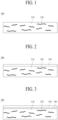
- FIG. 1 is a schematic diagram illustrating an optical film 100 according to an embodiment of the present disclosure.
- a film having light transmittance is referred to as an "optical film 100".
- the optical film 100 includes a light-transmitting matrix 110 and a filler 120 dispersed in the light-transmitting matrix 110.
- the light-transmitting matrix 110 may be light-transmissive. According to an embodiment of the present disclosure, the light-transmitting matrix 110 may be flexible.
- the optical film according to an embodiment of the present disclosure may be bendable, foldable, or rollable.
- the optical film 100 according to an embodiment of the present disclosure may be light-transmissive and may be bendable, foldable, or rollable.
- Physical properties that are used to confirm the reliability of flexible materials include mechanical properties such as strength, hardness, strain, and elastic modulus.
- the mechanical property of a material refers to the degree the material responds to an external stimulus, for example, the collation between external force and the deformation of the material caused thereby.
- the stress relaxation behavior may be evaluated using a universal tensile tester (UTM) or a dynamic mechanical analyzer (DMA).
- the light-transmitting matrix 110 may include at least one of an imide repeating unit or an amide repeating unit.
- the light-transmitting matrix 110 may be prepared from monomeric ingredients including dianhydrides and diamines.
- the light-transmitting matrix 110 may include an imide repeating unit formed by dianhydride and diamine.
- the light-transmitting matrix 110 may include a polyimide-based polymer.
- the polyimide-based polymer may include polyimide polymers, polyamide polymers, polyamide-imide polymers and the like.
- the light-transmitting matrix 110 according to an embodiment of the present disclosure may be formed of, for example, a polyamide-imide-based polymer resin.
- the light-transmitting matrix 110 may be prepared from a polymerizable composition.
- the polymerizable composition according to an embodiment of the present disclosure may contain a diamine-based monomer.
- the diamine monomer may include at least one of 2,2'-bis(trifluoromethyl)benzidine (TFDB), 4,4'-oxydianiline (ODA), p-phenylene diamine (pPDA), m-phenylene diamine (mPDA), p-methylene diamine (pMDA), m-methylene diamine (mMDA), 1,3-bis(3-aminophenoxy) benzene (133APB), 1,3-bis(4-aminophenoxy) benzene (134APB), 2,2'-bis[4(4-aminophenoxy)phenyl]hexafluoropropane (4BDAF), 2,2'-bis(3-aminophenyl)hexafluoropropane (33-6F), 2,2'-bis(4-aminophenyl)hexafluoropropane (44-6F), bis(4-aminophenyl)sulfone (4DDS), 2,2'-bis(trifluoromethyl
- the polymerizable composition according to an embodiment of the present disclosure may contain at least one of a dianhydride compound or a dicarbonyl compound.
- the dianhydride compound may, for example, include at least one of 3,3,4,4-biphenyltetracarboxylic dianhydride (BPDA), 2,2-bis(3,4-dicarboxyphenyl)hexafluoropropane dianhydride (6FDA), 4-(2,5-dioxotetrahydrofuran-3-yl)-1,2,3,4-tetrahydronaphthalene-1,2-dicarboxylic anhydride (TDA), 1,2,4,5-benzene tetracarboxylic dianhydride (pyromellitic dianhydride, PMDA), 3,3,4,4-benzophenone tetracarboxylic dianhydride (BTDA), 4,4-oxydiphthalic dianhydride (ODPA), bis(3,4-dicarboxyphenyl)dimethyl-silane dianhydride (SiDA), 4,4-bis(3,4-dicarboxyphenoxy)dipheny
- BPDA 3,3,4,
- the dicarbonyl compound may, for example, include at least one of terephthaloyl chloride (TPC), phthaloyl chloride, isophthaloyl chloride (IPC), 4,4'-biphenyldicarbonyl chloride (DPDOC), 4,4'-oxybis(benzoyl chloride) (OBBOC), naphthalene-2,3-dicarbonyl dichloride, or 1,4-cyclohexanedicabonyldichloride (CHDOC), but is not limited thereto.
- TPC terephthaloyl chloride
- IPC isophthaloyl chloride
- DPDOC 4,4'-biphenyldicarbonyl chloride
- OOBOC 4,4'-oxybis(benzoyl chloride)
- CHDOC 1,4-cyclohexanedicabonyldichloride
- the total equivalent weight of the dianhydride compound and the dicarbonyl compound may be substantially the same as the equivalent weight of the diamine monomer.
- the polymerizable composition according to an embodiment of the present disclosure may contain 60 mol% or more of the dicarbonyl compound with respect to the total number of moles of the dianhydride compound and the dicarbonyl compound to ensure excellent mechanical properties.
- the molar ratio of the dianhydride compound to the dicarbonyl compound may be within the range of 5:95 to 40:60.
- the filler 120 may have a fiber shape.
- the fiber may, for example, refer to a material whose length is much greater than the diameter thereof.
- the fiber may refer to a thin, long, thread-like material.
- the fiber may refer to a material with a linear structure.
- the fiber may also refer to a long and bendable material.
- a shape having a length greater than a diameter is referred to as a "fiber shape”.
- the fiber shape may also be referred to as a "filament shape”.
- the length of the filler 120 may be more than twice the diameter thereof.
- the filler 120 has a fiber shape and thus can engage (or link, or connect, or entangle) the polymer chains constituting the light-transmitting matrix 110.
- the stability and arrangement characteristics of the polymer chains can be improved, the mechanical properties of the light-transmitting matrix 110 can be improved, and the mechanical properties of the optical film 100 can also be improved.
- filler 120 There is no particular limitation on the type of filler 120. Any filler may be used without limitation as the filler 120 according to an embodiment of the present disclosure so long as it has a fiber shape.
- the filler 120 may be inorganic or organic.
- the filler 120 may include at least one of inorganic fibers, organic fibers, or organic-inorganic hybrid fibers.
- the filler 120 may have a fiber shape.
- the filler 120 may have a single-stranded fiber shape, a multi-stranded fiber shape, or a branch shape in which multiple strands are arranged in the form of branches based on one central strand.
- the filler 120 may include at least one of a glass fiber, an aluminum-based fiber, or a fluoride fiber.
- the glass fiber may contain SiO 2 and may further contain other components in addition to SiO 2 .
- the aluminum-based fiber may contain aluminum oxide hydroxide or Al 2 O 3 .
- the aluminum-based fiber may further contain other components in addition to aluminum oxide hydroxide or Al 2 O 3 .
- the fluoride fiber may contain at least one of polytetrafluoroethylene (PTFE) or polyvinylidene fluoride (PVDF), and may further contain other components in addition to PTFE and PVDF.
- PTFE polytetrafluoroethylene
- PVDF polyvinylidene fluoride
- the filler 120 may include at least one of aluminum oxide hydroxide, SiO 2 , Al 2 O 3 , polytetrafluoroethylene (PTFE), or polyvinylidene fluoride (PVDF).
- aluminum oxide hydroxide SiO 2 , Al 2 O 3
- PTFE polytetrafluoroethylene
- PVDF polyvinylidene fluoride
- the filler 120 may be surface-treated.
- the filler 120 may be fiber surface-treated with an organic compound having an alkoxy group.
- the aluminum-based fiber may include at least one of aluminum oxide hydroxide or Al 2 O 3 .
- Aluminum oxide hydroxide is also called “Boehmite” and can be represented by ⁇ -AlO(OH). More specifically, aluminum oxide hydroxide may include a structure represented by any of the following formulas 1, 2, and 3. wherein n ranges from 50 to 10,000, m ranges from 50 to 10,000, and p ranges from 100 to 20,000.
- the filler 120 may be represented by any one of Formulas 4, 5 and 6.
- Formula 1 may be represented by, for example, Formula 4 below.
- Formula 4 below corresponds to the structure of Formula 1 wherein n is 5.
- Formula 2 may be represented by, for example, Formula 5 below.
- Formula 5 below corresponds to the structure of Formula 2 wherein m is 4.
- Formula 3 may be represented by, for example, Formula 6 below.
- Formula 6 below corresponds to the structure of Formula 3 wherein p is 3.
- Al 2 O 3 may have a unit structure represented by Formula 7 below.
- SiO 2 may have a unit structure represented by Formula 8 below.
- the filler 120 may have a diameter of 2 to 10 nm and a length of 200 nm to 4,000 nm.
- the diameter and length of the filler 120 may be measured with a transmission electron microscope (TEM).
- TEM transmission electron microscope
- the stability of the filler 120 may decrease and the filler may be cut or broken, thus contaminating the optical film 100 and increasing the haze of the optical film 100.
- the diameter of the filler 120 is higher than 10 nm, the filler 120 has difficulty in having a fiber shape and the optical film 100 may have deteriorated function of engaging polymer chains and decreased light transmittance.
- the length of the filler 120 When the length of the filler 120 is less than 200 nm, the function of the filler 120 to engage polymer chains may not be sufficiently exerted. When the length of the filler 120 is higher than 4,000 nm, the dispersibility of the filler 120 may decrease, and as a result, agglomeration of the filler 120 may occur within the light-transmitting matrix 110. Accordingly, the light transmittance of the optical film 100 may decrease and haze thereof may increase, and the optical properties of the optical film 100 may deteriorate.
- the length of the filler 120 may be adjusted by growth or post-treatment conditions of the filler 120.
- the length of the filler 120 can be appropriately adjusted by controlling the temperature when growing the filler 120.
- ultrasonic waves or other energy may be applied to the filler 120 grown to a predetermined length so that the filler 120 is cut to a predetermined length.
- the filler 120 may cause appropriate light scattering to improve the optical properties of the optical film 100.
- the filler 120 may improve tensile properties. As a result, greater force is required to elongate the optical film 100 by the same length. Accordingly, the mechanical properties of the optical film 100 can be improved.
- the yield point of the optical film 100 may be lowered and the elasticity of the optical film 100 may be insufficient.
- the improvement in the mechanical properties of the optical film 100 may be insufficient.
- the content of the filler 120 in the optical film 100 may be adjusted within an appropriate range.
- the filler 120 may be added in an amount of 2 to 20 wt% of the solid content of the polymerizable composition. Specifically, the filler 120 may be added in an amount of 3 to 15 wt% of the solid content of the polymerizable composition. More specifically, the filler 120 may be added in an amount of 3 to 10 wt% of the solid content of the polymerizable composition.
- the mechanical properties of the optical film 100 can be improved by adjusting the content of the filler 120 and improving the dispersion method.
- the driving toughness and elastic limit of the optical film 100 may be improved.
- the optical film 100 may undergo almost no deterioration in mechanical properties even after treatment under high temperature and high humidity conditions. Accordingly, by adjusting the content of the filler 120 and improving the dispersion method, weather resistance and long-term stability as well as mechanical properties of the optical film 100 can be improved.
- the optical film 100 according to an embodiment of the present disclosure may have excellent driving toughness.
- Driving toughness refers to the product of an area of an elastic region in the strain-stress curve and a length (mm) of a specimen for the optical film 100.
- high driving toughness means that a high force is required to deform a specimen until plastic deformation occurs due to a wide elastic zone.
- the specimen for the optical film 100 may be produced to have a length (L) x width (W) x thickness (T) of 5 mm x 2 mm x 0.05 mm.
- the unit of driving toughness is MPa ⁇ mm.
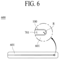
- FIG. 6 is a cross-sectional view illustrating an exterior appearance of a display device according to another embodiment of the present disclosure. More specifically, FIG. 6 is a schematic side view illustrating a foldable display device in a folded state.
- a display device 600 may include an optical film 100 according to one embodiment of the present disclosure and a case 601.
- the display device 600 may be a bendable or foldable device, such as a foldable display device.
- R means the radius of curvature.
- the optical film 100 when the display device 600 including the optical film 100 according to an embodiment of the present disclosure is folded, the optical film 100 may be bent by a radius of curvature (R) of 1.5 mm, based on a thickness of 50 ⁇ m.
- R radius of curvature
- a space 701 may be formed by the bent optical film 100.
- the strain (%) of the outermost of the optical film 100 is 1.6%. Accordingly, the driving toughness of the optical film 100 can be obtained based on the strain of 1.6% of the outermost of the optical film 100.
- the driving toughness is obtained by measuring a ratio of strain to stress of the optical film 100 using a dynamic mechanical analyzer (DMA), obtaining a strain-stress curve using the strain of the optical film 100 on the x-axis and the stress of the optical film 100 on the y-axis, and calculating the product of an area with a strain of 1.6% or less in the strain-stress curve, by the length of the specimen.
- DMA dynamic mechanical analyzer
- the optical film 100 may be disposed on the display device 600 and may be thus used under various environmental conditions for a long period of time.
- the optical film 100 may be deformed when it is repeatedly folded and unfolded under various environmental conditions. To prevent this deformation, it is necessary for the optical film to maintain elasticity under strain or stress conditions.
- the ability to maintain driving toughness may be evaluated after the optical film 100 is treated under harsh conditions, for example, high temperature and high humidity conditions.
- the optical film 100 may be manufactured such that the change in driving toughness is reduced after treatment under room temperature and humidity conditions and then treatment under high temperature and high humidity conditions.
- the optical film 100 may have a first driving toughness of 240 MPa ⁇ mm or more.
- the first driving toughness refers to driving toughness measured after treatment under room temperature and humidity conditions.
- the treatment under room temperature and humidity conditions means that the optical film 100 is allowed to stand at a temperature of 25°C ⁇ 3°C and humidity of 30% ⁇ 5% for 1 hour.
- the optical film 100 may not be able to resist external force well under room temperature and humidity conditions and may be deformed.
- the optical film 100 when used as a cover window for a foldable device, it may be repeatedly folded and unfolded for a long period of time and deformation may occur in the folded part and visibility may be deteriorated.
- the optical film 100 when the optical film 100 is pressed by external force, a mark is easily left even by a mild stimulus corresponding to a 1H pencil hardness level and may not be restored over time.
- the optical film 100 according to an embodiment of the present disclosure may have a second driving toughness of 217 MPa ⁇ mm or more.
- the second driving toughness refers to driving toughness measured after treatment under high temperature and high humidity conditions.
- the treatment under high temperature and high humidity conditions means that the optical film is allowed to stand at a temperature of 60°C ⁇ 3°C and a humidity of 90% ⁇ 5% for 1 hour.
- the optical film 100 may not be able to resist external force well under high temperature and high humidity conditions and thus may be deformed.
- the optical film 100 is used as a cover window for a foldable device, it is repeatedly folded and unfolded in a state in which it is heated while high-definition videos are played and the folded area may be deformed and visibility may be reduced.
- the optical film 100 may have a driving toughness change index of 10.5% or less.
- the driving toughness change index refers to the change to the driving toughness (second driving toughness) of the optical film after treatment at high temperature and humidity from the driving toughness (first driving toughness) of the optical film after treatment at room temperature and humidity.
- a small driving toughness change index means that the optical film has excellent mechanical properties at high temperature and high humidity.
- the driving toughness change index is calculated in accordance with Equation 1 below.
- the unit of driving toughness change index is %.
- Driving toughness change index % First driving toughness ⁇ Second driving toughness First driving toughness ⁇ 100
- the driving toughness change index is higher than 10.5%, the stress greatly may decrease as temperature and humidity increase and thus the optical film may be inapplicable to a foldable device.
- the optical film 100 may have a first driving elastic limit of 155 MPa ⁇ mm or more.
- driving elastic limit refers to a ratio of a force required to deform a material to a strain and indicates force required to deform a material at 1%.
- a film having a great driving elastic limit may exhibit excellent toughness and strength.
- the unit of the driving elastic limit is MPa ⁇ mm.
- the first driving elastic limit is calculated in accordance with Equation 2 below.
- First driving elastic limit first driving toughness /first driving strain rate
- the first driving strain rate is 1.6%.
- the first driving strain rate is limited to 1.6% which corresponds to the strain of the outermost of the film when the radius of curvature (R) of a 50 ⁇ m thick film is 1.5 mm.
- the optical film 100 is easily deformed due to low resistance to external force.
- the optical film 100 may have a second driving elastic limit of 140 MPa ⁇ mm or more.
- Second driving elastic limit second driving toughness/second driving strain rate
- the second driving strain rate is 1.6%.
- the first driving strain rate is limited to 1.6% which corresponds to the strain of the outermost of the film when the radius of curvature (R) of a 50 ⁇ m thick film is 1.5 mm.
- the optical film 100 is easily deformed by external forces at high temperature and humidity.
- the optical film 100 may have a modulus of 7.5 GPa or more.
- the modulus of the optical film 100 according to an embodiment of the present disclosure may be measured on an optical film sample with a size of 10 mm x 100 mm using a universal tensile tester in accordance with ASTM D885.
- the universal tensile tester may be MODEL 5967 from Instron Corp.
- the filler 120 has a fiber shape and can engage polymer chains constituting the light-transmitting matrix 110. As a result, the stability and arrangement characteristics of polymer chains are improved and intermolecular attraction is increased, so that the optical film 100 has a high modulus of 7.5 GPa or more.
- the optical film 100 may have a modulus of 8.0 GPa or more, and may have a modulus of 9.0 GPa or more.
- the light-transmitting matrix 110 may have a thickness sufficient to protect the display panel.
- the light-transmitting matrix 110 may have a thickness of 10 to 100 ⁇ m.
- the thickness of the light-transmitting matrix 110 may be the same as the thickness of the optical film 100.
- FIG. 2 is a schematic diagram illustrating a cover window substrate 200 according to another embodiment of the present disclosure.
- the cover window substrate 200 according to another embodiment of the present disclosure may include an optical film 100 according to an embodiment of the present disclosure.
- the cover window substrate 200 may further include a coating layer 130 on a light-transmitting sheet in order to improve the surface properties of the light transmissive matrix and the cover window substrate 200.
- the light-transmitting matrix may include an optical film 100 according to an embodiment of the present disclosure.
- FIG. 3 is a schematic diagram illustrating a cover window substrate 300 according to another embodiment of the present disclosure.
- the cover window substrate 300 according to another embodiment of the present disclosure further includes a primer layer 140 between the light-transmitting sheet and the coating layer 130 in order to improve adhesion between the light-transmitting sheet and the coating layer 130.
- FIGS. 4 and 5 a display device 400 using the optical film 100 according to an embodiment of the present disclosure will be described with reference to FIGS. 4 and 5 .
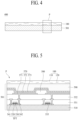
- FIG. 4 is a cross-sectional view illustrating a part of a display device 400 according to another embodiment of the present disclosure and FIG. 5 is an enlarged cross-sectional view of "P" in FIG. 4 .
- the display device 400 includes a display panel 501 and an optical film 100 on the display panel 501.
- the display panel 501 includes a substrate 510, a thin film transistor TFT on the substrate 510, and an organic light-emitting device 570 connected to the thin film transistor TFT.
- the organic light-emitting device 570 includes a first electrode 571, an organic light-emitting layer 572 on the first electrode 571, and a second electrode 573 on the organic light-emitting layer 572.
- the display device 400 shown in FIGs. 4 and 5 is an organic light-emitting display device.
- the substrate 510 may be formed of glass or plastic. Specifically, the substrate 510 may be formed of plastic such as a polyimide-based resin or an optical film. Although not shown, a buffer layer may be disposed on the substrate 510.
- the thin film transistor TFT is disposed on the substrate 510.
- the thin film transistor TFT includes a semiconductor layer 520, a gate electrode 530 that is insulated from the semiconductor layer 520 and at least partially overlaps the semiconductor layer 520, a source electrode 541 connected to the semiconductor layer 520, and a drain electrode 542 that is spaced apart from the source electrode 541 and is connected to the semiconductor layer 520.
- a gate insulating layer 535 is disposed between the gate electrode 530 and the semiconductor layer 520.
- An interlayer insulating layer 551 may be disposed on the gate electrode 530, and a source electrode 541 and a drain electrode 542 may be disposed on the interlayer insulating layer 551.
- a planarization layer 552 is disposed on the thin film transistor TFT to planarize the top of the thin film transistor TFT.
- a first electrode 571 is disposed on the planarization layer 552.
- the first electrode 571 is connected to the thin film transistor TFT through a contact hole provided in the planarization layer 552.
- a bank layer 580 is disposed on the planarization layer 552 in a part of the first electrode 571 to define pixel areas or light-emitting areas.
- the bank layer 580 is disposed in the form of a matrix at the boundaries between a plurality of pixels to define the respective pixel regions.
- the organic light-emitting layer 572 is disposed on the first electrode 571.
- the organic light-emitting layer 572 may also be disposed on the bank layer 580.
- the organic light-emitting layer 572 may include one light-emitting layer, or two or more light-emitting layers stacked in a vertical direction. Light having any one color among red, green, and blue may be emitted from the organic light-emitting layer 572, and white light may be emitted therefrom.
- the second electrode 573 is disposed on the organic light-emitting layer 572.
- the first electrode 571, the organic light-emitting layer 572, and the second electrode 573 may be stacked to constitute the organic light-emitting device 570.
- each pixel may include a color filter for filtering the white light emitted from the organic light-emitting layer 572 based on a particular wavelength.
- the color filter is formed on the light path.
- a thin-film encapsulation layer 590 may be disposed on the second electrode 573.
- the thin-film encapsulation layer 590 may include at least one organic layer and at least one inorganic layer, and the at least one organic layer and the at least one inorganic layer may be alternately disposed.
- the optical film 100 may be disposed on the display panel 501 having the stack structure described above.
- the optical film 100 may include a light-transmitting matrix 110 and a filler 120 dispersed in the light-transmitting matrix 110.
- cover window substrates 200 and 300 may be disposed on the display panel 501 having the laminated structure described above.
- the cover window substrates 200 and 300 may include an optical film 100 according to an embodiment of the present disclosure.
- the method of manufacturing an optical film 100 includes primarily dispersing the filler 120 in a polymerizable composition for forming a light-transmitting matrix 110 to prepare a first mix solution, and casting the first mixture solution to produce a cast film.
- a polyimide-based resin solution may be used as the polymerizable composition for forming the light-transmitting matrix 110.
- the method of manufacturing the optical film 100 includes preparing a polyimide-based resin powder, dissolving the polyimide-based resin powder in a first solvent to prepare a polyimide-based resin solution, dispersing the filler 120 in a second solvent to prepare a filler dispersion, and mixing the dispersion with the polyimide-based resin solution to prepare a first mix solution.
- DMAc N,N-dimethylacetamide
- DMAc N,N-dimethylacetamide
- MEK methyl ethyl ketone
- the filler 120 having a fiber shape for example, the fiber-shape filler 120 having a high aspect ratio, has a length greater than a diameter thereof and may easily cause aggregation or agglomeration within the light-transmitting matrix. Therefore, the filler 120 requires excellent dispersibility in the first mix solution.
- PTSA p-toluene sulfonic acid
- the embodiment of the present disclosure is not limited thereto and other known additives may be used to improve the dispersibility of the filler 120.
- the pH of the first mix solution may be adjusted.
- the pH of the first mix solution may be adjusted to the range of 5 to 7. Accordingly, aggregation or agglomeration of the filler 120 may be prevented.
- the first mix solution is cast, dried and heat-treated to form an optical film 100.
- the film formed by casting the first mix solution may be referred to as a "cast film” and the film produced by drying and heat-treating the cast film may be referred to as an "optical film 100".
- the cast film can be referred to as an "uncured film”.
- casting may be performed by bar coating.
- the orientation direction and degree of orientation of the filler 120 can be controlled by adjusting the pressure applied to the cast film formed by casting.
- convection may be prevented during drying and heat treatment of the cast film formed by casting, so that the filler 120 may be oriented in a certain direction.
- the orientation of the filler 120 may decrease.
- the cast film may be allowed to be dried slowly to prevent convection.
- drying of the cast film may be performed while raising the temperature from 80°C to 120°C at a rate of 1°C/1 minute.
- the orientation of the filler 120 may be fixed.
- TFDB bis(trifluoromethyl) benzidine
- DMAc dimethylacetamide
- BPDA biphenyl tetracarboxylic dianhydride
- 6FDA 2,2-bis(3,4-dicarboxyphenyl)hexafluoropropane dianhydride
- reaction tank was lowered to 7°C or lower, and then 118.77g of terephthaloyl chloride (TPC) and propylene oxide (PO) were added thereto.
- TPC terephthaloyl chloride
- PO propylene oxide
- a 4-neck double-jacketed reaction tank under a nitrogen atmosphere was connected to a circulator to maintain the temperature of the reaction tank at 5°C, and then 5 parts by weight of the filler 120 was added with respect to 100 parts by weight of the total weight of the polyimide resin powder and 525.17 g of DMAc (first solvent) in the reaction tank, followed by stirring for a predetermined period of time. Then, 85.97 g of the solid powder of the polyimide-based polymerizable composition prepared in Preparation Example was added thereto and stirred until it was dissolved to prepare a polyimide-based resin solution.
- the filler 120 was a fiber-shape of alumina hydrate including the structure of Formula 1.
- the pH measured immediately after preparing the polyimide resin solution was 8 or higher.
- a weak acid such as acetic acid was added to the polyimide resin solution and the pH of the polyimide resin solution was adjusted to be within the range of 5 to 7.
- the polyimide-based resin solution thus prepared was a polyimide-based resin solution in which the fibrous filler 120 was dispersed.
- the obtained polyimide-based resin solution was cast.
- a casting substrate was used for casting.
- the casting substrate may be a glass substrate, a stainless steel (SUS) substrate, a Teflon substrate, or the like. According to one embodiment of the present disclosure, a glass substrate was used as the casting substrate.
- the obtained polyimide-based resin solution was applied to a glass substrate and cast.
- the first mix solution was applied to the glass substrate (casting substrate) and cast while applying a force of 30 N in a direction perpendicular to the glass substrate. As a result, a cast film was produced.
- the cast film was produced by slowly drying in a hot air oven at 80°C up to 120°C at a rate of 1°C/min for about 40 minutes to maintain the orientation of the filler 120. Then, the produced film was peeled off of the glass substrate and fixed to a frame with pins.
- the frame to which the optical film was fixed was slowly heated in a vacuum oven from 100°C to 280°C for 2 hours, cooled slowly and separated from the frame to obtain an optical film.
- the optical film was heated again at 250°C for 5 minutes.
- an optical film 100 having a thickness of 50 ⁇ m and including a light-transmitting matrix 110 and an alumina-based filler 120 dispersed in the light-transmitting matrix 110 was completed.
- the optical films 100 were produced under the conditions of Table 1 in the same manner as in Example 1 and were respectively referred to as "Examples 2 to 8".
- the optical films 100 were produced under the conditions of Table 1 in the same manner as in Example 1 except for addition of the filler, and were respectively referred to as "Comparative Examples 1 to 3".
- Table 1 Item Diamine monomer Dianhydride compound Dicarbonyl compound Type of filler Content of filler TFDB BPDA CBDA 6FDA TPC
- Example 1 100 27 - 12 61 Alumina hydrate (Formula 1) 5
- Example 2 100 27 - 12 61 Alumina hydrate (Formula 1) 10
- Example 3 100 - 17 17 66 Alumina hydrate (Formula 1) 7
- Example 4 100 - 17 17 66 Alumina hydrate (Formula 1) 10
- Example 5 100 - 26.25 12.5 61.25 Alumina hydrate (Formula 1) 3
- Example 6 100 - 26.25 12.5 61.25 Alumina hydrate (Formula 1) 5
- Example 7 100 27 - 12 61 Alumina hydrate (Formula 2)
- Example 8 100 27 - 12 61 Alumina
- Alumina hydrate (Formulas 1, 2, and 3) fillers 4 nm in diameter and 1,500 nm in length.
- strain-stress curves of the optical films manufactured according to Examples 1 to 8 and Comparative Examples 1 to 3 were measured using a dynamic mechanical analysis (DMA) model DMA850 from TA Instruments.
- DMA dynamic mechanical analysis
- the point where the stress pattern changes rapidly in the strain-stress curve of the optical film measured in (1) above was defined as a yield point. Specifically, the point at which stress begins to decrease or remain constant despite an increase in strain was set as the yield point. The unit of yield point is %.
- the area of the strain-stress curve was calculated three times based on the strain of 1.6% in the strain-stress curve measured in (1) above, the average of the three measured areas was multiplied by the length of the specimen and the result was defined as a driving toughness.
- the unit of driving toughness is MPa ⁇ mm.
- the first driving toughness is determined by measuring the area of the strain-stress curve based on the strain of 1.6% in the strain-stress curve after treatment under room temperature and high humidity conditions and the second driving toughness is determined by measuring the area of the strain-stress curve based on the strain of 1.6% in the strain-stress curve after treatment under high temperature and high humidity conditions.
- Driving toughness change index % First driving toughness ⁇ Second driving toughness First driving toughness ⁇ 100
- the area of the strain-stress curve at a strain of 1.6% in the strain-stress curve measured in (1) above was defined as the driving toughness and a ratio of the driving toughness to the driving strain rate was defined as the driving elastic limit.
- the first and second driving strain rates are set as 1.6% which corresponds to the strain of the outermost of the film when the radius of curvature (R) of a 50 ⁇ m thick film is 1.5R.
- the measurement was performed three times and the average of the three measured values was determined as the driving elasticity limit.
- the unit of the driving elastic limit is MPa ⁇ mm.
- First driving elastic limit first driving toughness /first driving strain rate
- the first driving elasticity limit is measured after the optical film specimen is treated under room temperature and humidity conditions.
- Second driving elastic limit second driving toughness/second driving strain rate
- the second driving elasticity limit is measured after the optical film specimen is treated under high temperature and humidity conditions.
- modulus of each of the optical films manufactured according to Examples 1 to 8 and Comparative Examples 1 to 3 was measured in accordance with ASTM D885 using an Instron universal tensile tester (MODEL 5967).
- Example 1 2.52 2.95 255 242 5.3 160 151 8.0
- Example 2 1.86 2.69 333 319 4.1 208 199 9.3
- Example 3 1.74 2.11 418 376 10.0 261 235 8.4
- Example 4 1.31 1.71 459 424 7.7 287 265 9.3
- Example 5 1.61 1.96 371 332 10.4 232 208 7.5
- Example 6 1.09 1.36 451 418 7.2 282 261 8.4
- Example 7 2.41 2.52 232 244 5.4 145 153 7.8
- Example 8 2.74 2.69 233 239 2.7 145 149 10.0 Comparati ve Example 1 3.14 3.94 239 93.5 60.9 150 58.4 5.9 Comparati ve Example 2 2.45 2.24 370 294 20.5 232 184 6.0 Comparati ve Example 3 1.
- the optical film 100 according to an embodiment of the present disclosure has excellent driving toughness, excellent driving toughness change index, excellent driving elastic limit, and excellent driving elastic limit index, and thus exhibits excellent mechanical properties.
- Optical film 110 Light-transmitting matrix
- Filler 130 Coating layer
- 140 Primer layer 200
- 300 Cover window substrate 400
- 600 Display device 501: Display panel
Landscapes
- Chemical & Material Sciences (AREA)
- Health & Medical Sciences (AREA)
- Chemical Kinetics & Catalysis (AREA)
- Medicinal Chemistry (AREA)
- Polymers & Plastics (AREA)
- Organic Chemistry (AREA)
- Engineering & Computer Science (AREA)
- Manufacturing & Machinery (AREA)
- Materials Engineering (AREA)
- Inorganic Chemistry (AREA)
- Compositions Of Macromolecular Compounds (AREA)
- Devices For Indicating Variable Information By Combining Individual Elements (AREA)
- Manufacture Of Macromolecular Shaped Articles (AREA)
- Laminated Bodies (AREA)
- Macromolecular Compounds Obtained By Forming Nitrogen-Containing Linkages In General (AREA)
Abstract
Description
- The present disclosure relates to an optical film and a display device including the same and more particularly, to an optical film having a low driving toughness change index and excellent weather resistance.
- Recently, the use of an optical film instead of glass as a cover window of a display device has been considered with the goal of reducing thickness and weight and increasing the flexibility of the display device. In order for the optical film to be usable as a cover window of a display device, the optical film needs to have superior optical properties and excellent mechanical properties. For example, an optical film needs to have properties such as excellent strength, hardness, abrasion resistance, and flexibility.
- Fillers may be added in order to impart desired physical properties to an optical film requiring various physical properties. The fillers may vary depending on physical properties required for the optical film.
- Therefore, the present disclosure has been made in view of the above problems, and it is one aspect of the present disclosure to provide an optical film that includes a fiber-shape filler dispersed in a light-transmitting matrix.
- It is another aspect of the present disclosure to provide an optical film that includes a fiber-shape filler dispersed in a light-transmitting matrix and thereby exhibits excellent driving toughness.
- It is another aspect of the present disclosure to provide an optical film that includes a fiber-shape filler dispersed in a light-transmitting matrix and thereby exhibits excellent driving toughness change index.
- It is another aspect of the present disclosure to provide an optical film that includes a fiber-shape filler dispersed in a light-transmitting matrix and thereby exhibits excellent driving elastic limit.
- It is another aspect of the present disclosure to provide a cover window substrate including the optical film.
- It is another aspect of the present disclosure to provide a display device including the optical film.
- In accordance with one aspect of the present disclosure, provided is an optical film including a light-transmitting matrix and a filler dispersed in the light-transmitting matrix,
- wherein the filler has a fiber shape and a driving toughness change index of 10.5% or less, wherein the driving toughness change index is calculated in accordance with Equation 1 below:

- wherein the first driving toughness is driving toughness measured after treatment under room temperature and humidity conditions,
- the treatment under room temperature and humidity conditions is performed by allowing the optical film to stand at a temperature of 25°C ± 3°C and humidity of 30% ± 5% for 1 hour,
- the second driving toughness is driving toughness measured after treatment under high temperature and humidity conditions,
- the treatment under high temperature and humidity conditions is performed by allowing the optical film to stand at a temperature of 60°C ± 3°C and humidity of 90% ± 5% for 1 hour, and
- the driving toughness is defined by measuring a ratio of strain to stress of the optical film using a dynamic mechanical analyzer (DMA), obtaining a strain-stress curve using the strain of the optical film on an x-axis and the stress of the optical film on a y-axis, and calculating a product of an area at a strain of 1.6% or less in the strain-stress curve, by a length of a specimen.
- The optical film may have a first driving toughness of 240 MPa·mm or more.
- The optical film may have a second driving toughness of 217 MPa·mm or more.
- The optical film may have a first driving elastic limit of 155 MPa·mm or more, wherein the first driving elastic limit is calculated in accordance with Equation 2 below:
First driving elastic limit = first driving toughness / first driving strain rate - The optical film may have a second driving elastic limit of 140 MPa·mm or more, wherein the second driving elastic limit is calculated in accordance with Equation 3 below:
Second driving elastic limit = second driving toughness / second driving strain rate - The filler may include at least one of glass fiber, aluminum-based fiber, or fluoride fiber.
- The filler may include at least one of aluminum oxide hydroxide, SiO2, Al2O3, polytetrafluoroethylene (PTFE), or polyvinylidene fluoride (PVDF).
- The light-transmitting matrix may be produced from a polymerizable composition, and may contain a diamine monomer, and at least one of a dianhydride compound or a dicarbonyl compound.
- The light-transmitting matrix may include at least one of an imide repeating unit or an amide repeating unit.
- The diamine monomer may include at least one of 2,2'-bis(trifluoromethyl)benzidine (TFDB), 4,4'-oxydianiline (ODA), p-phenylene diamine (pPDA), m-phenylene diamine (mPDA), p-methylene diamine (pMDA), m-methylene diamine (mMDA), 1,3-bis(3-aminophenoxy)benzene (133APB), 1,3-bis(4-aminophenoxy)benzene (134APB), 2,2'-bis[4(4-aminophenoxy)phenyl]hexafluoropropane (4BDAF), 2,2'-bis(3-aminophenyl)hexafluoropropane (33-6F), 2,2'-bis(4-aminophenyl)hexafluoropropane (44-6F), bis(4-aminophenyl)sulfone (4DDS), bis(aminophenyl)sulfone (3DDS), 1,3-cyclohexanediamine (13CHD), 1,4-cyclohexanediamine (14CHD), 2,2-bis[4-(4-aminophenoxy)-phenyl]propane (6HMDA), 2,2-bis(3-amino-4-hydroxy-phenyl)-hexafluoropropane (DBOH), or 4,4'-bis(3-aminophenoxy)diphenyl sulfone (DBSDA).
- The dianhydride compound may include at least one of 3,3,4,4-biphenyltetracarboxylic dianhydride (BPDA), 2,2-bis(3,4-dicarboxyphenyl)hexafluoropropane dianhydride (6FDA), 4-(2,5-dioxotetrahydrofuran-3-yl)-1,2,3,4-tetrahydronaphthalene-1,2-dicarboxylic anhydride (TDA), 1,2,4,5-benzene tetracarboxylic dianhydride (pyromellitic dianhydride, PMDA), 3,3,4,4-benzophenone tetracarboxylic dianhydride (BTDA), 4,4-oxydiphthalic dianhydride (ODPA), bis(3,4-dicarboxyphenyl)dimethyl-silane dianhydride (SiDA), 4,4-bis(3,4-dicarboxyphenoxy)diphenyl sulfide dianhydride (BDSDA), sulfonyl diphthalic anhydride (SO2DPA), cyclobutane-1,2,3,4-tetracarboxylic dianhydride (CBDA), or 4,4'-(4,4'-isopropylidenediphenoxy)bis(phthalic anhydride) (6HBDA).
- The dicarbonyl compound may include at least one of terephthaloyl chloride (TPC), phthaloyl chloride, isophthaloyl chloride (IPC), 4,4'-biphenyldicarbonyl chloride (DPDOC), 4,4'-oxybis (benzoyl chloride) (OBBOC), naphthalene-2,3-dicarbonyl dichloride, or 1,4-cyclohexanedicabonyldichloride (CHDOC).
- A molar ratio of the dianhydride compound to the dicarbonyl compound may fall within a range of 5:95 to 40:60.
- In accordance with another aspect of the present disclosure, provided is a cover window substrate including the optical film.
- In accordance with another aspect of the present disclosure, provided is a cover window substrate including a light-transmitting sheet and a coating layer disposed on the light-transmitting sheet, wherein the light-transmitting sheet includes the optical film.
- The cover window substrate may further include a primer layer between the light-transmitting sheet and the coating layer.
- In accordance with another aspect of the present disclosure, provided is a display device including a display panel and the optical film disposed on the display panel.
- According to one embodiment of the present disclosure, the filler included in the optical film has a fiber shape and can engage polymer chains constituting the light-transmitting matrix. As a result, the optical film can exhibit superior mechanical strength, particularly, excellent driving toughness and driving toughness change index.
- In addition, according to an embodiment of the present disclosure, the optical film can exhibit excellent driving elastic limit and driving elastic limit index.
- According to an embodiment of the present disclosure, the optical film containing a fiber filler may exhibit excellent mechanical properties in addition to excellent optical properties. The optical film according to an embodiment of the present disclosure may exhibit excellent optical and mechanical properties, thus being useful as a cover window of a display device.
-
-
FIG. 1 is a schematic diagram illustrating an optical film according to an embodiment of the present disclosure. -
FIG. 2 is a schematic diagram illustrating a cover window substrate according to another embodiment of the present disclosure. -
FIG. 3 is a schematic diagram illustrating a cover window substrate according to yet another embodiment of the present disclosure. -
FIG. 4 is a cross-sectional view illustrating a part of a display device according to another embodiment of the present disclosure. -
FIG. 5 is an enlarged cross-sectional view illustrating part "P" inFIG. 4 . -
FIG. 6 is a cross-sectional view illustrating an exterior appearance of a display device according to another embodiment of the present disclosure. -
FIG. 7 is a strain-stress curve after treatment under room temperature and humidity conditions in Examples 1 and 2 and Comparative Example 1. -
FIG. 8 is a strain-stress curve after treatment under high temperature and high humidity conditions in Examples 1 and 2 and Comparative Example 1. -
FIG. 9 is a strain-stress curve after treatment under room temperature and humidity conditions in Examples 3 and 4 and Comparative Example 2. -
FIG. 10 is a strain-stress curve after treatment under high temperature and high humidity conditions in Examples 3 and 4 and Comparative Example 2. -
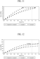
FIG. 11 is a strain-stress curve after treatment under room temperature and humidity conditions in Examples 5 and 6 and Comparative Example 3. -
FIG. 12 is a strain-stress curve after treatment under high temperature and high humidity conditions in Examples 5 and 6 and Comparative Example 3. - Hereinafter, embodiments of the present disclosure will be described in detail with reference to the accompanying drawings. However, the following embodiments are illustratively provided merely for clear understanding of the present disclosure and do not limit the scope of the present disclosure.
- The shapes, sizes, ratios, angles, and numbers disclosed in the drawings for describing embodiments of the present disclosure are merely examples, and the present disclosure is not limited to the illustrated details. Like reference numerals refer to like elements throughout the present specification. In the following description, when a detailed description of relevant known functions or configurations is determined to unnecessarily obscure important points of the present disclosure, the detailed description will be omitted.
- In the case in which a term such as "comprise", "have", or "include" is used in the present specification, another part may also be present, unless "only" is also used. Terms in a singular form may include the plural meanings, unless noted to the contrary. Also, in construing an element, the element is to be construed as including an error range, even if there is no explicit description thereof.
- In describing a positional relationship, for example, when the positional relationship is described using "on", "above", "below", or "next to", the case of no contact therebetween may be included, unless "immediately" or "directly" is used.
- Spatially relative terms, such as "below", "beneath", "lower", "above", and "upper", may be used herein to describe the relationship between a device or element and another device or element, as shown in the FIG.s. It will be understood that spatially relative terms are intended to encompass different orientations of a device during the use or operation of the device, in addition to the orientation depicted in the FIG.s. For example, if a device in one of the FIG.s is turned upside down, elements described as "below" or "beneath" other elements would then be positioned "above" the other elements. The exemplary term "below" or "beneath" can, therefore, encompass the meanings of both "below" and "above". In the same manner, the exemplary term "above" or "upper" can encompass the meanings of both "above" and "below".
- In describing temporal relationships, for example, when a temporal order is described using "after", "subsequent", "next", or "before", the case of a non-continuous relationship may be included, unless "immediately" or "directly" is used.
- It will be understood that, although the terms "first", "second", etc. may be used herein to describe various elements, these elements are not limited by these terms. These terms are only used to distinguish one element from another. Therefore, a first element could be termed a second element within the technical idea of the present disclosure.
- It should be understood that the term "at least one" includes all combinations related with one or more items. For example, "at least one among a first element, a second element, and a third element" may include all combinations of two or more elements selected from among the first, second, and third elements, as well as each of the first, second, and third elements.
- Features of various embodiments of the present disclosure may be partially or completely integrated or combined with each other, and may be variously interoperated with each other and driven technically. The embodiments of the present disclosure may be carried out independently from each other, or may be carried out together in an interrelated manner.
-
FIG. 1 is a schematic diagram illustrating anoptical film 100 according to an embodiment of the present disclosure. According to one embodiment of the present disclosure, a film having light transmittance is referred to as an "optical film 100". - The
optical film 100 according to an embodiment of the present disclosure includes a light-transmittingmatrix 110 and afiller 120 dispersed in the light-transmittingmatrix 110. - The light-transmitting
matrix 110 according to an embodiment of the present disclosure may be light-transmissive. According to an embodiment of the present disclosure, the light-transmittingmatrix 110 may be flexible. For example, the optical film according to an embodiment of the present disclosure may be bendable, foldable, or rollable. As a result, theoptical film 100 according to an embodiment of the present disclosure may be light-transmissive and may be bendable, foldable, or rollable. - Physical properties that are used to confirm the reliability of flexible materials include mechanical properties such as strength, hardness, strain, and elastic modulus. The mechanical property of a material refers to the degree the material responds to an external stimulus, for example, the collation between external force and the deformation of the material caused thereby. To determine the deformation of a material, to which external force is applied, for example, the stress relaxation behavior may be evaluated using a universal tensile tester (UTM) or a dynamic mechanical analyzer (DMA).
- According to an embodiment of the present disclosure, the light-transmitting
matrix 110 may include at least one of an imide repeating unit or an amide repeating unit. - The light-transmitting
matrix 110 according to an embodiment of the present disclosure may be prepared from monomeric ingredients including dianhydrides and diamines. Specifically, the light-transmittingmatrix 110 may include an imide repeating unit formed by dianhydride and diamine. - However, the light-transmitting
matrix 110 according to an embodiment of the present disclosure is not limited thereto, and the light-transmittingmatrix 110 may be produced from monomeric ingredients including a dicarbonyl compound in addition to dianhydride and diamine. The light-transmittingmatrix 110 according to an embodiment of the present disclosure may have an imide repeating unit and an amide repeating unit. For example, the light-transmittingmatrix 110 having an imide repeating unit and an amide repeating unit may be a polyamide-imide resin. - According to one embodiment of the present disclosure, the light-transmitting
matrix 110 may include a polyimide-based polymer. Examples of the polyimide-based polymer may include polyimide polymers, polyamide polymers, polyamide-imide polymers and the like. The light-transmittingmatrix 110 according to an embodiment of the present disclosure may be formed of, for example, a polyamide-imide-based polymer resin. - According to one embodiment, the light-transmitting
matrix 110 may be prepared from a polymerizable composition. - The polymerizable composition according to an embodiment of the present disclosure may contain a diamine-based monomer.
- According to one embodiment of the present disclosure, the diamine monomer, for example, may include at least one of 2,2'-bis(trifluoromethyl)benzidine (TFDB), 4,4'-oxydianiline (ODA), p-phenylene diamine (pPDA), m-phenylene diamine (mPDA), p-methylene diamine (pMDA), m-methylene diamine (mMDA), 1,3-bis(3-aminophenoxy) benzene (133APB), 1,3-bis(4-aminophenoxy) benzene (134APB), 2,2'-bis[4(4-aminophenoxy)phenyl]hexafluoropropane (4BDAF), 2,2'-bis(3-aminophenyl)hexafluoropropane (33-6F), 2,2'-bis(4-aminophenyl)hexafluoropropane (44-6F), bis(4-aminophenyl)sulfone (4DDS), bis(aminophenyl) sulfone (3DDS), 1,3-cyclohexanediamine (13CHD), 1,4-cyclohexanediamine (14CHD), 2,2-bis[4-(4-aminophenoxy)-phenyl]propane (6HMDA), 2,2-bis(3-amino-4-hydroxy-phenyl)-hexafluoropropane (DBOH), and 4,4'-bis(3-aminophenoxy)diphenyl sulfone (DBSDA), but is not limited thereto.
- The polymerizable composition according to an embodiment of the present disclosure may contain at least one of a dianhydride compound or a dicarbonyl compound.
- According to one embodiment of the present disclosure, the dianhydride compound may, for example, include at least one of 3,3,4,4-biphenyltetracarboxylic dianhydride (BPDA), 2,2-bis(3,4-dicarboxyphenyl)hexafluoropropane dianhydride (6FDA), 4-(2,5-dioxotetrahydrofuran-3-yl)-1,2,3,4-tetrahydronaphthalene-1,2-dicarboxylic anhydride (TDA), 1,2,4,5-benzene tetracarboxylic dianhydride (pyromellitic dianhydride, PMDA), 3,3,4,4-benzophenone tetracarboxylic dianhydride (BTDA), 4,4-oxydiphthalic dianhydride (ODPA), bis(3,4-dicarboxyphenyl)dimethyl-silane dianhydride (SiDA), 4,4-bis(3,4-dicarboxyphenoxy)diphenyl sulfide dianhydride (BDSDA), sulfonyl diphthalic anhydride (SO2DPA), cyclobutane-1,2,3,4-tetracarboxylic dianhydride (CBDA), or 4,4'-(4,4'-isopropylidenediphenoxy)bis(phthalic anhydride) (6HBDA), but is not limited thereto.
- According to one embodiment of the present disclosure, the dicarbonyl compound may, for example, include at least one of terephthaloyl chloride (TPC), phthaloyl chloride, isophthaloyl chloride (IPC), 4,4'-biphenyldicarbonyl chloride (DPDOC), 4,4'-oxybis(benzoyl chloride) (OBBOC), naphthalene-2,3-dicarbonyl dichloride, or 1,4-cyclohexanedicabonyldichloride (CHDOC), but is not limited thereto.
- According to one embodiment of the present disclosure, the total equivalent weight of the dianhydride compound and the dicarbonyl compound may be substantially the same as the equivalent weight of the diamine monomer.
- The polymerizable composition according to an embodiment of the present disclosure may contain 60 mol% or more of the dicarbonyl compound with respect to the total number of moles of the dianhydride compound and the dicarbonyl compound to ensure excellent mechanical properties.
- For example, the molar ratio of the dianhydride compound to the dicarbonyl compound may be within the range of 5:95 to 40:60.
- According to one embodiment of the present disclosure, the
filler 120 may have a fiber shape. For example, the fiber may, for example, refer to a material whose length is much greater than the diameter thereof. The fiber may refer to a thin, long, thread-like material. The fiber may refer to a material with a linear structure. The fiber may also refer to a long and bendable material. - Hereinafter, a shape having a length greater than a diameter is referred to as a "fiber shape". The fiber shape may also be referred to as a "filament shape". According to one embodiment of the present disclosure, the length of the
filler 120 may be more than twice the diameter thereof. - According to one embodiment of the present disclosure, the
filler 120 has a fiber shape and thus can engage (or link, or connect, or entangle) the polymer chains constituting the light-transmittingmatrix 110. As a result, the stability and arrangement characteristics of the polymer chains can be improved, the mechanical properties of the light-transmittingmatrix 110 can be improved, and the mechanical properties of theoptical film 100 can also be improved. - There is no particular limitation on the type of
filler 120. Any filler may be used without limitation as thefiller 120 according to an embodiment of the present disclosure so long as it has a fiber shape. Thefiller 120 may be inorganic or organic. Thefiller 120 may include at least one of inorganic fibers, organic fibers, or organic-inorganic hybrid fibers. - More specifically, the
filler 120 may have a fiber shape. For example, thefiller 120 may have a single-stranded fiber shape, a multi-stranded fiber shape, or a branch shape in which multiple strands are arranged in the form of branches based on one central strand. - According to one embodiment of the present disclosure, the
filler 120 may include at least one of a glass fiber, an aluminum-based fiber, or a fluoride fiber. - The glass fiber may contain SiO2 and may further contain other components in addition to SiO2. The aluminum-based fiber may contain aluminum oxide hydroxide or Al2O3. The aluminum-based fiber may further contain other components in addition to aluminum oxide hydroxide or Al2O3. The fluoride fiber may contain at least one of polytetrafluoroethylene (PTFE) or polyvinylidene fluoride (PVDF), and may further contain other components in addition to PTFE and PVDF.
- According to one embodiment of the present disclosure, the
filler 120 may include at least one of aluminum oxide hydroxide, SiO2, Al2O3, polytetrafluoroethylene (PTFE), or polyvinylidene fluoride (PVDF). - According to one embodiment of the present disclosure, the
filler 120 may be surface-treated. For example, thefiller 120 may be fiber surface-treated with an organic compound having an alkoxy group. - According to one embodiment of the present disclosure, the aluminum-based fiber may include at least one of aluminum oxide hydroxide or Al2O3. Aluminum oxide hydroxide is also called "Boehmite" and can be represented by γ-AlO(OH). More specifically, aluminum oxide hydroxide may include a structure represented by any of the following formulas 1, 2, and 3.


- When the structures of Formulas 1, 2 and 3 are expanded for better understanding of the structure of the
filler 120, thefiller 120 may be represented by any one of Formulas 4, 5 and 6. - The structure represented by Formula 1 may be represented by, for example, Formula 4 below. Formula 4 below corresponds to the structure of Formula 1 wherein n is 5.


- The structure represented by Formula 2 may be represented by, for example, Formula 5 below. Formula 5 below corresponds to the structure of Formula 2 wherein m is 4.

- The structure represented by Formula 3 may be represented by, for example, Formula 6 below. Formula 6 below corresponds to the structure of Formula 3 wherein p is 3.


- In Formulas 4 to 6, "*" represents a binding position.
- According to an embodiment of the present disclosure, Al2O3 may have a unit structure represented by Formula 7 below.
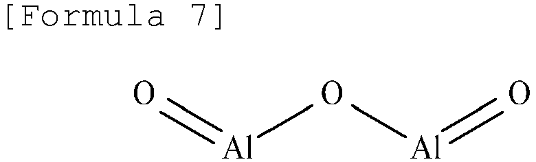
- According to an embodiment of the present disclosure, SiO2 may have a unit structure represented by Formula 8 below.

- According to one embodiment of the present disclosure, the
filler 120 may have a diameter of 2 to 10 nm and a length of 200 nm to 4,000 nm. - According to one embodiment of the present disclosure, the diameter and length of the
filler 120 may be measured with a transmission electron microscope (TEM). - When the diameter of the
filler 120 is less than 2 nm, the stability of thefiller 120 may decrease and the filler may be cut or broken, thus contaminating theoptical film 100 and increasing the haze of theoptical film 100. When the diameter of thefiller 120 is higher than 10 nm, thefiller 120 has difficulty in having a fiber shape and theoptical film 100 may have deteriorated function of engaging polymer chains and decreased light transmittance. - When the length of the
filler 120 is less than 200 nm, the function of thefiller 120 to engage polymer chains may not be sufficiently exerted. When the length of thefiller 120 is higher than 4,000 nm, the dispersibility of thefiller 120 may decrease, and as a result, agglomeration of thefiller 120 may occur within the light-transmittingmatrix 110. Accordingly, the light transmittance of theoptical film 100 may decrease and haze thereof may increase, and the optical properties of theoptical film 100 may deteriorate. - According to one embodiment of the present disclosure, the length of the
filler 120 may be adjusted by growth or post-treatment conditions of thefiller 120. For example, the length of thefiller 120 can be appropriately adjusted by controlling the temperature when growing thefiller 120. In addition, ultrasonic waves or other energy may be applied to thefiller 120 grown to a predetermined length so that thefiller 120 is cut to a predetermined length. - According to an embodiment of the present disclosure, the
filler 120 may cause appropriate light scattering to improve the optical properties of theoptical film 100. - According to an embodiment of the present disclosure, the
filler 120 may improve tensile properties. As a result, greater force is required to elongate theoptical film 100 by the same length. Accordingly, the mechanical properties of theoptical film 100 can be improved. - However, when the content of the
filler 120 is excessive, the yield point of theoptical film 100 may be lowered and the elasticity of theoptical film 100 may be insufficient. When the content of thefiller 120 is small, the improvement in the mechanical properties of theoptical film 100 may be insufficient. - Therefore, in order to obtain appropriate strength and elasticity of the
optical film 100, the content of thefiller 120 in theoptical film 100 may be adjusted within an appropriate range. - For example, the
filler 120 may be added in an amount of 2 to 20 wt% of the solid content of the polymerizable composition. Specifically, thefiller 120 may be added in an amount of 3 to 15 wt% of the solid content of the polymerizable composition. More specifically, thefiller 120 may be added in an amount of 3 to 10 wt% of the solid content of the polymerizable composition. - According to an embodiment of the present disclosure, the mechanical properties of the
optical film 100 can be improved by adjusting the content of thefiller 120 and improving the dispersion method. For example, the driving toughness and elastic limit of theoptical film 100 may be improved. In addition, theoptical film 100 may undergo almost no deterioration in mechanical properties even after treatment under high temperature and high humidity conditions. Accordingly, by adjusting the content of thefiller 120 and improving the dispersion method, weather resistance and long-term stability as well as mechanical properties of theoptical film 100 can be improved. - The
optical film 100 according to an embodiment of the present disclosure may have excellent driving toughness. - Driving toughness refers to the product of an area of an elastic region in the strain-stress curve and a length (mm) of a specimen for the
optical film 100. For example, high driving toughness means that a high force is required to deform a specimen until plastic deformation occurs due to a wide elastic zone. For example, the specimen for theoptical film 100 may be produced to have a length (L) x width (W) x thickness (T) of 5 mm x 2 mm x 0.05 mm. The unit of driving toughness is MPa·mm. - In the strain-stress curve, a part where a stress increases at a constant rate as a strain increases and thus a slope is almost constant is defined as an "elastic region", and the deformation of a material within this region is defined as "elastic deformation". On the other hand, a part where the slope and curve shape rapidly change is defined as a "plastic region", and it is considered that plastic deformation starts as dislocation occurs in the internal structure of the material.
-
FIG. 6 is a cross-sectional view illustrating an exterior appearance of a display device according to another embodiment of the present disclosure. More specifically,FIG. 6 is a schematic side view illustrating a foldable display device in a folded state. - Referring to
FIG. 6 , adisplay device 600 according to another embodiment of the present disclosure may include anoptical film 100 according to one embodiment of the present disclosure and acase 601. Thedisplay device 600 may be a bendable or foldable device, such as a foldable display device. In addition, R means the radius of curvature. - As shown in
FIG. 6 , when thedisplay device 600 including theoptical film 100 according to an embodiment of the present disclosure is folded, theoptical film 100 may be bent by a radius of curvature (R) of 1.5 mm, based on a thickness of 50 µm. In addition, aspace 701 may be formed by the bentoptical film 100. - When the
optical film 100 according to an embodiment of the present disclosure is bent by a radius of curvature (R) of 1.5 mm based on a thickness of 50 µm, the strain (%) of the outermost of theoptical film 100 is 1.6%. Accordingly, the driving toughness of theoptical film 100 can be obtained based on the strain of 1.6% of the outermost of theoptical film 100. - More specifically, the driving toughness is obtained by measuring a ratio of strain to stress of the
optical film 100 using a dynamic mechanical analyzer (DMA), obtaining a strain-stress curve using the strain of theoptical film 100 on the x-axis and the stress of theoptical film 100 on the y-axis, and calculating the product of an area with a strain of 1.6% or less in the strain-stress curve, by the length of the specimen. - According to another embodiment of the present disclosure, the
optical film 100 may be disposed on thedisplay device 600 and may be thus used under various environmental conditions for a long period of time. Theoptical film 100 may be deformed when it is repeatedly folded and unfolded under various environmental conditions. To prevent this deformation, it is necessary for the optical film to maintain elasticity under strain or stress conditions. - In order to evaluate the ability of the
optical film 100 to maintain elasticity, the ability to maintain driving toughness may be evaluated after theoptical film 100 is treated under harsh conditions, for example, high temperature and high humidity conditions. - According to one embodiment of the present disclosure, the
optical film 100 may be manufactured such that the change in driving toughness is reduced after treatment under room temperature and humidity conditions and then treatment under high temperature and high humidity conditions. - The
optical film 100 according to an embodiment of the present disclosure may have a first driving toughness of 240 MPa·mm or more. - The first driving toughness refers to driving toughness measured after treatment under room temperature and humidity conditions.
- The treatment under room temperature and humidity conditions means that the
optical film 100 is allowed to stand at a temperature of 25°C ± 3°C and humidity of 30% ± 5% for 1 hour. - When the first driving toughness is less than 240 MPa·mm, the
optical film 100 may not be able to resist external force well under room temperature and humidity conditions and may be deformed. For example, when theoptical film 100 is used as a cover window for a foldable device, it may be repeatedly folded and unfolded for a long period of time and deformation may occur in the folded part and visibility may be deteriorated. In addition, when theoptical film 100 is pressed by external force, a mark is easily left even by a mild stimulus corresponding to a 1H pencil hardness level and may not be restored over time. - The
optical film 100 according to an embodiment of the present disclosure may have a second driving toughness of 217 MPa·mm or more. - The second driving toughness refers to driving toughness measured after treatment under high temperature and high humidity conditions.
- The treatment under high temperature and high humidity conditions means that the optical film is allowed to stand at a temperature of 60°C ± 3°C and a humidity of 90% ± 5% for 1 hour.
- When the second driving toughness is less than 217 MPa·mm, the
optical film 100 may not be able to resist external force well under high temperature and high humidity conditions and thus may be deformed. For example, when theoptical film 100 is used as a cover window for a foldable device, it is repeatedly folded and unfolded in a state in which it is heated while high-definition videos are played and the folded area may be deformed and visibility may be reduced. - The
optical film 100 according to an embodiment of the present disclosure may have a driving toughness change index of 10.5% or less. - The driving toughness change index refers to the change to the driving toughness (second driving toughness) of the optical film after treatment at high temperature and humidity from the driving toughness (first driving toughness) of the optical film after treatment at room temperature and humidity. For example, a small driving toughness change index means that the optical film has excellent mechanical properties at high temperature and high humidity.
- The driving toughness change index is calculated in accordance with Equation 1 below. The unit of driving toughness change index is %.

- When the driving toughness change index is higher than 10.5%, the stress greatly may decrease as temperature and humidity increase and thus the optical film may be inapplicable to a foldable device.
- The
optical film 100 according to an embodiment of the present disclosure may have a first driving elastic limit of 155 MPa·mm or more. - The term "driving elastic limit" refers to a ratio of a force required to deform a material to a strain and indicates force required to deform a material at 1%. For example, a film having a great driving elastic limit may exhibit excellent toughness and strength. The unit of the driving elastic limit is MPa·mm.
- The first driving elastic limit is calculated in accordance with Equation 2 below.
First driving elastic limit = first driving toughness /first driving strain rate - The first driving strain rate is 1.6%. The first driving strain rate is limited to 1.6% which corresponds to the strain of the outermost of the film when the radius of curvature (R) of a 50 µm thick film is 1.5 mm.
- When the first driving elastic limit is less than 155 MPa·mm, the
optical film 100 is easily deformed due to low resistance to external force. - The
optical film 100 according to an embodiment of the present disclosure may have a second driving elastic limit of 140 MPa·mm or more. - The second driving elastic limit is calculated in accordance with Equation 3 below.
Second driving elastic limit = second driving toughness/second driving strain rate - The second driving strain rate is 1.6%. The first driving strain rate is limited to 1.6% which corresponds to the strain of the outermost of the film when the radius of curvature (R) of a 50 µm thick film is 1.5 mm.
- When the second driving elastic limit is less than 140 MPa·mm, the
optical film 100 is easily deformed by external forces at high temperature and humidity. - The
optical film 100 according to an embodiment of the present disclosure may have a modulus of 7.5 GPa or more. - The modulus of the
optical film 100 according to an embodiment of the present disclosure may be measured on an optical film sample with a size of 10 mm x 100 mm using a universal tensile tester in accordance with ASTM D885. For example, the universal tensile tester may be MODEL 5967 from Instron Corp. - In general, it is known that it is difficult for a film formed of a polymer resin to achieve a modulus of 6.0 GPa or more. However, according to one embodiment of the present disclosure, the
filler 120 has a fiber shape and can engage polymer chains constituting the light-transmittingmatrix 110. As a result, the stability and arrangement characteristics of polymer chains are improved and intermolecular attraction is increased, so that theoptical film 100 has a high modulus of 7.5 GPa or more. - More specifically, the
optical film 100 according to an embodiment of the present disclosure may have a modulus of 8.0 GPa or more, and may have a modulus of 9.0 GPa or more. - The light-transmitting
matrix 110 according to an embodiment of the present disclosure may have a thickness sufficient to protect the display panel. For example, the light-transmittingmatrix 110 may have a thickness of 10 to 100 µm. The thickness of the light-transmittingmatrix 110 may be the same as the thickness of theoptical film 100. -
FIG. 2 is a schematic diagram illustrating acover window substrate 200 according to another embodiment of the present disclosure. - The
cover window substrate 200 according to another embodiment of the present disclosure may include anoptical film 100 according to an embodiment of the present disclosure. - The
cover window substrate 200 according to another embodiment of the present disclosure may further include acoating layer 130 on a light-transmitting sheet in order to improve the surface properties of the light transmissive matrix and thecover window substrate 200. The light-transmitting matrix may include anoptical film 100 according to an embodiment of the present disclosure. -
FIG. 3 is a schematic diagram illustrating acover window substrate 300 according to another embodiment of the present disclosure. - The
cover window substrate 300 according to another embodiment of the present disclosure further includes aprimer layer 140 between the light-transmitting sheet and thecoating layer 130 in order to improve adhesion between the light-transmitting sheet and thecoating layer 130. - Hereinafter, a
display device 400 using theoptical film 100 according to an embodiment of the present disclosure will be described with reference toFIGS. 4 and 5 . -
FIG. 4 is a cross-sectional view illustrating a part of adisplay device 400 according to another embodiment of the present disclosure andFIG. 5 is an enlarged cross-sectional view of "P" inFIG. 4 . - Referring to
FIG. 4 , thedisplay device 400 according to another embodiment of the present disclosure includes adisplay panel 501 and anoptical film 100 on thedisplay panel 501. - Referring to
FIGs. 4 and 5 , thedisplay panel 501 includes asubstrate 510, a thin film transistor TFT on thesubstrate 510, and an organic light-emittingdevice 570 connected to the thin film transistor TFT. The organic light-emittingdevice 570 includes afirst electrode 571, an organic light-emittinglayer 572 on thefirst electrode 571, and asecond electrode 573 on the organic light-emittinglayer 572. Thedisplay device 400 shown inFIGs. 4 and 5 is an organic light-emitting display device. - The
substrate 510 may be formed of glass or plastic. Specifically, thesubstrate 510 may be formed of plastic such as a polyimide-based resin or an optical film. Although not shown, a buffer layer may be disposed on thesubstrate 510. - The thin film transistor TFT is disposed on the
substrate 510. The thin film transistor TFT includes asemiconductor layer 520, agate electrode 530 that is insulated from thesemiconductor layer 520 and at least partially overlaps thesemiconductor layer 520, asource electrode 541 connected to thesemiconductor layer 520, and adrain electrode 542 that is spaced apart from thesource electrode 541 and is connected to thesemiconductor layer 520. - Referring to
FIG. 5 , agate insulating layer 535 is disposed between thegate electrode 530 and thesemiconductor layer 520. An interlayer insulatinglayer 551 may be disposed on thegate electrode 530, and asource electrode 541 and adrain electrode 542 may be disposed on theinterlayer insulating layer 551. - A
planarization layer 552 is disposed on the thin film transistor TFT to planarize the top of the thin film transistor TFT. - A
first electrode 571 is disposed on theplanarization layer 552. Thefirst electrode 571 is connected to the thin film transistor TFT through a contact hole provided in theplanarization layer 552. - A
bank layer 580 is disposed on theplanarization layer 552 in a part of thefirst electrode 571 to define pixel areas or light-emitting areas. For example, thebank layer 580 is disposed in the form of a matrix at the boundaries between a plurality of pixels to define the respective pixel regions. - The organic light-emitting
layer 572 is disposed on thefirst electrode 571. The organic light-emittinglayer 572 may also be disposed on thebank layer 580. The organic light-emittinglayer 572 may include one light-emitting layer, or two or more light-emitting layers stacked in a vertical direction. Light having any one color among red, green, and blue may be emitted from the organic light-emittinglayer 572, and white light may be emitted therefrom. - The
second electrode 573 is disposed on the organic light-emittinglayer 572. - The
first electrode 571, the organic light-emittinglayer 572, and thesecond electrode 573 may be stacked to constitute the organic light-emittingdevice 570. - Although not shown, when the organic light-emitting
layer 572 emits white light, each pixel may include a color filter for filtering the white light emitted from the organic light-emittinglayer 572 based on a particular wavelength. The color filter is formed on the light path. - A thin-
film encapsulation layer 590 may be disposed on thesecond electrode 573. The thin-film encapsulation layer 590 may include at least one organic layer and at least one inorganic layer, and the at least one organic layer and the at least one inorganic layer may be alternately disposed. - The
optical film 100 according to an embodiment of the present disclosure may be disposed on thedisplay panel 501 having the stack structure described above. Theoptical film 100 may include a light-transmittingmatrix 110 and afiller 120 dispersed in the light-transmittingmatrix 110. - In addition,
cover window substrates display panel 501 having the laminated structure described above. Thecover window substrates optical film 100 according to an embodiment of the present disclosure. - Hereinafter, a method of manufacturing an
optical film 100 according to another embodiment of the present disclosure will be described. - The method of manufacturing an
optical film 100 according to an embodiment of the present disclosure includes primarily dispersing thefiller 120 in a polymerizable composition for forming a light-transmittingmatrix 110 to prepare a first mix solution, and casting the first mixture solution to produce a cast film. - According to one embodiment of the present disclosure, a polyimide-based resin solution may be used as the polymerizable composition for forming the light-transmitting
matrix 110. - More specifically, the method of manufacturing the
optical film 100 according to an embodiment of the present disclosure includes preparing a polyimide-based resin powder, dissolving the polyimide-based resin powder in a first solvent to prepare a polyimide-based resin solution, dispersing thefiller 120 in a second solvent to prepare a filler dispersion, and mixing the dispersion with the polyimide-based resin solution to prepare a first mix solution. - DMAc (N,N-dimethylacetamide) may be used as the first solvent. DMAc (N,N-dimethylacetamide) or methyl ethyl ketone (MEK) may be used as the second solvent, but one embodiment of the present disclosure is not limited thereto, and other known solvents as the first solvent and the second solvent may be used.
- The
filler 120 having a fiber shape, for example, the fiber-shape filler 120 having a high aspect ratio, has a length greater than a diameter thereof and may easily cause aggregation or agglomeration within the light-transmitting matrix. Therefore, thefiller 120 requires excellent dispersibility in the first mix solution. - According to one embodiment of the present disclosure, to improve the dispersibility of the
filler 120, for example, p-toluene sulfonic acid (PTSA) may be used as an additive. However, the embodiment of the present disclosure is not limited thereto and other known additives may be used to improve the dispersibility of thefiller 120. - According to one embodiment of the present disclosure, to improve the dispersibility of the
filler 120, for example, the pH of the first mix solution may be adjusted. For example, the pH of the first mix solution may be adjusted to the range of 5 to 7. Accordingly, aggregation or agglomeration of thefiller 120 may be prevented. - Next, the first mix solution is cast, dried and heat-treated to form an
optical film 100. According to one embodiment of the present disclosure, the film formed by casting the first mix solution may be referred to as a "cast film" and the film produced by drying and heat-treating the cast film may be referred to as an "optical film 100". The cast film can be referred to as an "uncured film". - In order to improve the orientation of the
filler 120, casting may be performed by bar coating. - According to one embodiment of the present disclosure, the orientation direction and degree of orientation of the
filler 120 can be controlled by adjusting the pressure applied to the cast film formed by casting. - In addition, convection may be prevented during drying and heat treatment of the cast film formed by casting, so that the
filler 120 may be oriented in a certain direction. - Specifically, when convection is generated inside the cast film that is dried using heat, the orientation of the
filler 120 may decrease. Thus, the cast film may be allowed to be dried slowly to prevent convection. For example, drying of the cast film may be performed while raising the temperature from 80°C to 120°C at a rate of 1°C/1 minute. When drying is performed over a certain level, the orientation of thefiller 120 may be fixed. - Hereinafter, the present disclosure will be described in more detail with reference to preparation examples and examples. However, the following preparation examples and examples should not be construed as limiting the scope of the present disclosure.
- 320.23 g of bis(trifluoromethyl) benzidine (TFDB) was dissolved in dimethylacetamide (DMAc) in a 4-neck double jacketed reactor. Then, 79.44 g of biphenyl tetracarboxylic dianhydride (BPDA) was added thereto and stirred for 2 hours while maintaining the temperature of the reaction tank at 25°C to allow a reaction to occur. After the reaction was completed, 53.31 g of 2,2-bis(3,4-dicarboxyphenyl)hexafluoropropane dianhydride (6FDA) was added and stirred for 1 hour while maintaining the temperature of the reaction tank at 25°C to allow a reaction to occur.
- Then, the temperature of the reaction tank was lowered to 7°C or lower, and then 118.77g of terephthaloyl chloride (TPC) and propylene oxide (PO) were added thereto. The temperature of the reaction tank was maintained at 7°C and stirred for 1 hour, the temperature was elevated to room temperature, and the resulting product was allowed to stand for 24 hours.
- After the polymerization reaction was completed, 67.87 g of pyridine and 87.62 g of acetic anhydride were added to the obtained polymer solution, the temperature was raised to 80°C, and the mixture was stirred for 1 hour. The result was cooled again to room temperature, and 20 L of methanol was added to the obtained polymerizable composition solution to precipitate the solid. The precipitated solid was filtered and pulverized, washed again with 2 L of methanol, and then dried in vacuum at 100°C for 6 hours to obtain a polyimide-based polymerizable composition as a solid powder. The solid of the polyimide-based polymerizable composition thus prepared was a solid of polyamide-imide polymerizable composition. The yield was 80% or more.
- A 4-neck double-jacketed reaction tank under a nitrogen atmosphere was connected to a circulator to maintain the temperature of the reaction tank at 5°C, and then 5 parts by weight of the
filler 120 was added with respect to 100 parts by weight of the total weight of the polyimide resin powder and 525.17 g of DMAc (first solvent) in the reaction tank, followed by stirring for a predetermined period of time. Then, 85.97 g of the solid powder of the polyimide-based polymerizable composition prepared in Preparation Example was added thereto and stirred until it was dissolved to prepare a polyimide-based resin solution. Here, thefiller 120 was a fiber-shape of alumina hydrate including the structure of Formula 1. - The pH measured immediately after preparing the polyimide resin solution was 8 or higher. In order to improve the arrangement characteristics of the
filler 120, a weak acid such as acetic acid was added to the polyimide resin solution and the pH of the polyimide resin solution was adjusted to be within the range of 5 to 7. The polyimide-based resin solution thus prepared was a polyimide-based resin solution in which thefibrous filler 120 was dispersed. - The obtained polyimide-based resin solution was cast. A casting substrate was used for casting. At this time, there is no particular limitation on the type of the casting substrate. The casting substrate may be a glass substrate, a stainless steel (SUS) substrate, a Teflon substrate, or the like. According to one embodiment of the present disclosure, a glass substrate was used as the casting substrate.
- Specifically, the obtained polyimide-based resin solution was applied to a glass substrate and cast. In order to improve the orientation of the
filler 120, the first mix solution was applied to the glass substrate (casting substrate) and cast while applying a force of 30 N in a direction perpendicular to the glass substrate. As a result, a cast film was produced. - Specifically, the cast film was produced by slowly drying in a hot air oven at 80°C up to 120°C at a rate of 1°C/min for about 40 minutes to maintain the orientation of the
filler 120. Then, the produced film was peeled off of the glass substrate and fixed to a frame with pins. - The frame to which the optical film was fixed was slowly heated in a vacuum oven from 100°C to 280°C for 2 hours, cooled slowly and separated from the frame to obtain an optical film. The optical film was heated again at 250°C for 5 minutes.
- As a result, an
optical film 100 having a thickness of 50 µm and including a light-transmittingmatrix 110 and an alumina-basedfiller 120 dispersed in the light-transmittingmatrix 110 was completed. - The
optical films 100 were produced under the conditions of Table 1 in the same manner as in Example 1 and were respectively referred to as "Examples 2 to 8". - The
optical films 100 were produced under the conditions of Table 1 in the same manner as in Example 1 except for addition of the filler, and were respectively referred to as "Comparative Examples 1 to 3".[Table 1] Item Diamine monomer Dianhydride compound Dicarbonyl compound Type of filler Content of filler TFDB BPDA CBDA 6FDA TPC Example 1 100 27 - 12 61 Alumina hydrate (Formula 1) 5 Example 2 100 27 - 12 61 Alumina hydrate (Formula 1) 10 Example 3 100 - 17 17 66 Alumina hydrate (Formula 1) 7 Example 4 100 - 17 17 66 Alumina hydrate (Formula 1) 10 Example 5 100 - 26.25 12.5 61.25 Alumina hydrate (Formula 1) 3 Example 6 100 - 26.25 12.5 61.25 Alumina hydrate (Formula 1) 5 Example 7 100 27 - 12 61 Alumina hydrate (Formula 2) 5 Example 8 100 27 - 12 61 Alumina hydrate (Formula 3) 5 Comparati ve Example 1 100 27 - 12 61 None added - Comparati ve Example 2 100 - 17 17 66 None added - Comparati ve Example 3 100 - 26.25 12.5 61.25 None added - Alumina hydrate (Formulas 1, 2, and 3) fillers: 4 nm in diameter and 1,500 nm in length.
- The following measurements were performed on the optical films manufactured according to Examples 1 to 8 and Comparative Examples 1 to 3. In addition, the strain-stress curves of Examples 1 to 6 and Comparative Examples 1 to 3 are shown in
FIGS. 7 to 12 . - The strain-stress curves of the optical films manufactured according to Examples 1 to 8 and Comparative Examples 1 to 3 were measured using a dynamic mechanical analysis (DMA) model DMA850 from TA Instruments.
- an RH Chamber (constant temperature and humidity chamber) was connected to control the measurement environments.
- Measurement specimen: length (L) x width (W) x thickness (T) = 5 mm x 2 mm x 0.05 mm
- Treatment under room temperature and humidity conditions: conditions where the optical film specimens are allowed to stand at a temperature of 25°C±3°C and humidity of 30%±5% for 1 hour
- Measurement under high-temperature and high-humidity conditions: conditions where the optical film specimens are allowed to stand at a temperature of 60°C±3°C and humidity of 90%±5% for 1 hour
- The specimen of the optical film manufactured according to each of Examples 1 to 8 and Comparative Examples 1 to 3 was mounted on a film tension clamp and measured using strain sweep method among oscillation tests.
- The point where the stress pattern changes rapidly in the strain-stress curve of the optical film measured in (1) above was defined as a yield point. Specifically, the point at which stress begins to decrease or remain constant despite an increase in strain was set as the yield point. The unit of yield point is %.
- First yield point: Yield point on the strain-stress curve after treatment under room temperature and humidity conditions
- Second yield point: yield point in the strain-stress curve after treatment under high temperature and high humidity conditions.
- The area of the strain-stress curve was calculated three times based on the strain of 1.6% in the strain-stress curve measured in (1) above, the average of the three measured areas was multiplied by the length of the specimen and the result was defined as a driving toughness. The unit of driving toughness is MPa·mm.
- The first driving toughness is determined by measuring the area of the strain-stress curve based on the strain of 1.6% in the strain-stress curve after treatment under room temperature and high humidity conditions and the second driving toughness is determined by measuring the area of the strain-stress curve based on the strain of 1.6% in the strain-stress curve after treatment under high temperature and high humidity conditions.
- The degree of driving toughness change according to temperature and humidity changes in the optical films manufactured according to Examples 1 to 8 and Comparative Examples 1 to 3 was was defined as the driving toughness change index and was calculated in accordance with Equation 1 below. The unit of the driving toughness change index is %.

- The area of the strain-stress curve at a strain of 1.6% in the strain-stress curve measured in (1) above was defined as the driving toughness and a ratio of the driving toughness to the driving strain rate was defined as the driving elastic limit. The first and second driving strain rates are set as 1.6% which corresponds to the strain of the outermost of the film when the radius of curvature (R) of a 50 µm thick film is 1.5R.
- The measurement was performed three times and the average of the three measured values was determined as the driving elasticity limit. The unit of the driving elastic limit is MPa·mm.
- The first driving elastic limit and the second driving elastic limit were calculated in accordance with Equations 2 and 3 below:
First driving elastic limit = first driving toughness /first driving strain rate - The first driving elasticity limit is measured after the optical film specimen is treated under room temperature and humidity conditions.
- The second driving elastic limit is calculated in accordance with Equation 3 below.
Second driving elastic limit = second driving toughness/second driving strain rate - The second driving elasticity limit is measured after the optical film specimen is treated under high temperature and humidity conditions.
- The modulus of each of the optical films manufactured according to Examples 1 to 8 and Comparative Examples 1 to 3 was measured in accordance with ASTM D885 using an Instron universal tensile tester (MODEL 5967).
-
Load Cell 30 kN, Grip 250 N. -
Specimen size 10mm X 100 mm, tensile speed 25 mm/min - Since orientation occurs in a coating direction, the coating direction is referred to as "MD" and the direction perpendicular to the coating direction is referred to as "TD".
- Modulus unit: GPa
- The measurement results of physical properties are shown in Table 2 below.
[Table 2] Item First yield point Second yield point First driving toughnes s Second driving toughnes s Driving toughness variation index First driving elastic limit Second driving elastic limit Modulus (GPa) Example 1 2.52 2.95 255 242 5.3 160 151 8.0 Example 2 1.86 2.69 333 319 4.1 208 199 9.3 Example 3 1.74 2.11 418 376 10.0 261 235 8.4 Example 4 1.31 1.71 459 424 7.7 287 265 9.3 Example 5 1.61 1.96 371 332 10.4 232 208 7.5 Example 6 1.09 1.36 451 418 7.2 282 261 8.4 Example 7 2.41 2.52 232 244 5.4 145 153 7.8 Example 8 2.74 2.69 233 239 2.7 145 149 10.0 Comparati ve Example 1 3.14 3.94 239 93.5 60.9 150 58.4 5.9 Comparati ve Example 2 2.45 2.24 370 294 20.5 232 184 6.0 Comparati ve Example 3 1.80 2.41 330 284 14.1 206 177 6.5 - As can be seen from the results of measurement in Table 2, the
optical film 100 according to an embodiment of the present disclosure has excellent driving toughness, excellent driving toughness change index, excellent driving elastic limit, and excellent driving elastic limit index, and thus exhibits excellent mechanical properties. -
100: Optical film 110: Light-transmitting matrix 120: Filler 130: Coating layer 140: Primer layer 200, 300: Cover window substrate 400, 600: Display device 501: Display panel
Claims (17)
- An optical film, comprising:a light-transmitting matrix; anda filler dispersed in the light-transmitting matrix,wherein the filler has a fiber shape and a driving toughness change index of 10.5% or less,wherein the driving toughness change index is calculated in accordance with Equation 1 below:
 wherein the first driving toughness is driving toughness measured after treatment under room temperature and humidity conditions,the treatment under room temperature and humidity conditions is performed by allowing the optical film to stand at a temperature of 25°C ± 3°C and humidity of 30% ± 5% for 1 hour,the second driving toughness is driving toughness measured after treatment under high temperature and humidity conditions,the treatment under high temperature and humidity conditions is performed by allowing the optical film to stand at a temperature of 60°C ± 3°C and humidity of 90% ± 5% for 1 hour, andthe driving toughness is defined by measuring a ratio of strain to stress of the optical film using a dynamic mechanical analyzer (DMA), obtaining a strain-stress curve using the strain of the optical film on an x-axis and the stress of the optical film on a y-axis, and calculating a product of an area at a strain of 1.6% or less in the strain-stress curve, by a length of a specimen.
 - The optical film according to claim 1, wherein the optical film has a first driving toughness of 240 MPa·mm or more.
- The optical film according to claim 1, wherein the optical film has a second driving toughness of 217 MPa ·mm or more.
- The optical film according to claim 2, wherein the optical film has a first driving elastic limit of 155 MPa·mm or more,wherein the first driving elastic limit is calculated in accordance with Equation 2 below:
First driving elastic limit = first driving toughness /first driving strain rate wherein the first driving strain rate is 1.6%. - The optical film according to claim 3, wherein the optical film has a second driving elastic limit of 140 MPa·mm or more,wherein the second driving elastic limit is calculated in accordance with Equation 3 below:
Second driving elastic limit = second driving toughness/second driving strain rate wherein the second driving strain rate is 1.6%. - The optical film according to claim 1, wherein the filler comprises at least one of glass fiber, aluminum-based fiber, or fluoride fiber.
- The optical film according to claim 1, wherein the filler comprises at least one of aluminum oxide hydroxide, SiO2, Al2O3, polytetrafluoroethylene (PTFE), or polyvinylidene fluoride (PVDF).
- The optical film according to claim 1, wherein the light-transmitting matrix is produced from a polymerizable composition comprising:a diamine monomer; andat least one of a dianhydride compound or a dicarbonyl compound.
- The optical film according to claim 8, wherein the light-transmitting matrix comprises at least one of an imide repeating unit or an amide repeating unit.
- The optical film according to claim 8, wherein the diamine monomer comprises at least one of 2,2'-bis(trifluoromethyl)benzidine (TFDB), 4,4'-oxydianiline (ODA), p-phenylene diamine (pPDA), m-phenylene diamine (mPDA), p-methylene diamine (pMDA), m-methylene diamine (mMDA), 1,3-bis(3-aminophenoxy)benzene (133APB), 1,3-bis(4-aminophenoxy)benzene (134APB), 2,2'-bis[4(4-aminophenoxy)phenyl]hexafluoropropane (4BDAF), 2,2'-bis(3-aminophenyl)hexafluoropropane (33-6F), 2,2'-bis(4-aminophenyl)hexafluoropropane (44-6F), bis(4-aminophenyl)sulfone (4DDS), bis(aminophenyl)sulfone (3DDS), 1,3-cyclohexanediamine (13CHD), 1,4-cyclohexanediamine (14CHD), 2,2-bis[4-(4-aminophenoxy)-phenyl]propane (6HMDA), 2,2-bis(3-amino-4-hydroxy-phenyl)-hexafluoropropane (DBOH), or 4,4'-bis(3-aminophenoxy)diphenyl sulfone (DBSDA).
- The optical film according to claim 8, wherein the dianhydride compound comprises at least one of 3,3,4,4-biphenyltetracarboxylic dianhydride (BPDA), 2,2-bis(3,4-dicarboxyphenyl)hexafluoropropane dianhydride (6FDA), 4-(2,5-dioxotetrahydrofuran-3-yl)-1,2,3,4-tetrahydronaphthalene-1,2-dicarboxylic anhydride (TDA), 1,2,4,5-benzene tetracarboxylic dianhydride (pyromellitic dianhydride, PMDA), 3,3,4,4-benzophenone tetracarboxylic dianhydride (BTDA), 4,4-oxydiphthalic dianhydride (ODPA), bis(3,4-dicarboxyphenyl)dimethyl-silane dianhydride (SiDA), 4,4-bis(3,4-dicarboxyphenoxy)diphenyl sulfide dianhydride (BDSDA), sulfonyl diphthalic anhydride (SO2DPA), cyclobutane-1,2,3,4-tetracarboxylic dianhydride (CBDA), or 4,4'-(4,4'-isopropylidenediphenoxy)bis(phthalic anhydride) (6HBDA).
- The optical film according to claim 8, wherein the dicarbonyl compound comprises at least one of terephthaloyl chloride (TPC), phthaloyl chloride, isophthaloyl chloride (IPC), 4,4'-biphenyldicarbonyl chloride (DPDOC), 4,4'-oxybis (benzoyl chloride) (OBBOC), naphthalene-2,3-dicarbonyl dichloride, or 1,4-cyclohexanedicabonyldichloride (CHDOC).
- The optical film according to claim 8, wherein a molar ratio of the dianhydride compound to the dicarbonyl compound falls within a range of 5:95 to 40:60.
- A cover window substrate, comprising:
the optical film according to any one of claims 1 to 13. - A cover window substrate, comprising:a light-transmitting sheet; anda coating layer disposed on the light-transmitting sheet,wherein the light-transmitting sheet comprises the optical film according to any one of claims 1 to 13.
- The cover window substrate according to claim 15, further comprising:
a primer layer between the light-transmitting sheet and the coating layer. - A display device, comprising:a display panel; andthe optical film according to any one of claims 1 to 13 disposed on the display panel.
Applications Claiming Priority (3)
| Application Number | Priority Date | Filing Date | Title |
|---|---|---|---|
| KR20220123417 | 2022-09-28 | ||
| KR1020230126644A KR102819987B1 (en) | 2022-09-28 | 2023-09-21 | Optical film and display apparatus comprising the same |
| PCT/KR2023/014665 WO2024071909A1 (en) | 2022-09-28 | 2023-09-25 | Optical film and display device comprising same |
Publications (2)
| Publication Number | Publication Date |
|---|---|
| EP4564066A1 true EP4564066A1 (en) | 2025-06-04 |
| EP4564066A4 EP4564066A4 (en) | 2026-07-22 |
Family
ID=90478734
Family Applications (1)
| Application Number | Title | Priority Date | Filing Date |
|---|---|---|---|
| EP23873026.1A Pending EP4564066A4 (en) | 2022-09-28 | 2023-09-25 | OPTICAL FILM AND DISPLAY DEVICE WITH IT |
Country Status (5)
| Country | Link |
|---|---|
| EP (1) | EP4564066A4 (en) |
| JP (1) | JP2025532793A (en) |
| CN (1) | CN120129850A (en) |
| TW (1) | TWI870041B (en) |
| WO (1) | WO2024071909A1 (en) |
Cited By (1)
| Publication number | Priority date | Publication date | Assignee | Title |
|---|---|---|---|---|
| EP4538755A4 (en) * | 2022-07-18 | 2026-06-24 | Kolon Inc | OPTICAL FILM AND DISPLAY DEVICE WITH IT |
Family Cites Families (14)
| Publication number | Priority date | Publication date | Assignee | Title |
|---|---|---|---|---|
| JP2005025142A (en) * | 2003-07-04 | 2005-01-27 | Sony Corp | Light diffusion sheet, method for producing the same, and screen |
| US20070279741A1 (en) * | 2004-03-23 | 2007-12-06 | Nitto Denko Corporation | Polarizing Plate, Optical Film and Image Display |
| JPWO2008038714A1 (en) * | 2006-09-29 | 2010-01-28 | 大日本印刷株式会社 | Optical function film |
| JP5270106B2 (en) * | 2006-12-26 | 2013-08-21 | 株式会社クラレ | Polyamide resin composition and molded article comprising the same |
| EP2975163A4 (en) * | 2013-03-12 | 2016-10-19 | Japan Vilene Co Ltd | INORGANIC NANOFIBER AND PROCESS FOR PRODUCING THE SAME |
| JP2015044905A (en) * | 2013-08-27 | 2015-03-12 | 昭和電工株式会社 | Resin composition, transparent film, and production method and use of the same |
| JP5882510B2 (en) * | 2014-06-30 | 2016-03-09 | 太陽インキ製造株式会社 | Photosensitive dry film and method for producing printed wiring board using the same |
| JP2016044114A (en) * | 2014-08-27 | 2016-04-04 | 川研ファインケミカル株式会社 | Lipophilic alumina nanofiber having high aspect ratio and resin composite containing the same |
| KR102031556B1 (en) * | 2015-06-26 | 2019-10-14 | 동우 화인켐 주식회사 | Laminate film and display device comprising the same |
| KR101801471B1 (en) * | 2016-06-23 | 2017-11-24 | 동우 화인켐 주식회사 | Hard Coating Film and Image Display Device Using the Same |
| WO2021221118A1 (en) * | 2020-04-30 | 2021-11-04 | 太陽ホールディングス株式会社 | Resin composition and film using same |
| JP7620078B2 (en) * | 2020-07-10 | 2025-01-22 | コーロン インダストリーズ インク | Light-transmitting film, its manufacturing method, and display device including same |
| JP7471984B2 (en) * | 2020-09-30 | 2024-04-22 | 太陽ホールディングス株式会社 | Resin composition and film using same |
| TWI920444B (en) * | 2022-07-18 | 2026-04-01 | 南韓商可隆股份有限公司 | Optical film, display device and method of manufacturing optical film |
-
2023
- 2023-09-25 CN CN202380068923.8A patent/CN120129850A/en active Pending
- 2023-09-25 WO PCT/KR2023/014665 patent/WO2024071909A1/en not_active Ceased
- 2023-09-25 JP JP2025516073A patent/JP2025532793A/en active Pending
- 2023-09-25 EP EP23873026.1A patent/EP4564066A4/en active Pending
- 2023-09-27 TW TW112137037A patent/TWI870041B/en active
Cited By (1)
| Publication number | Priority date | Publication date | Assignee | Title |
|---|---|---|---|---|
| EP4538755A4 (en) * | 2022-07-18 | 2026-06-24 | Kolon Inc | OPTICAL FILM AND DISPLAY DEVICE WITH IT |
Also Published As
| Publication number | Publication date |
|---|---|
| JP2025532793A (en) | 2025-10-03 |
| EP4564066A4 (en) | 2026-07-22 |
| WO2024071909A1 (en) | 2024-04-04 |
| TWI870041B (en) | 2025-01-11 |
| TW202430587A (en) | 2024-08-01 |
| CN120129850A (en) | 2025-06-10 |
Similar Documents
| Publication | Publication Date | Title |
|---|---|---|
| KR102251516B1 (en) | Polyimide-polybenzoxazole precursor solution, polyimide-polybenzoxazole films, and process for producing thereof | |
| KR102426437B1 (en) | Polyamic acid, Polyimide Resin, Polyimide Film and Display Device Comprising Thereof | |
| JP6929355B2 (en) | Polyamic acid, polyimide, polyimide film, image display device containing this, and method for producing polyamic acid | |
| JP7487416B2 (en) | Optical film having improved optical properties, display device including the same, and method for manufacturing the same | |
| TWI870041B (en) | Optical film, cover window substrate and display device | |
| KR102675752B1 (en) | Polyamic acid-imide composition and polyimide film formed from the same | |
| WO2022102450A1 (en) | Colorless multilayer polyimide film, laminate body, and flexible electronic device manufacturing method | |
| KR102819987B1 (en) | Optical film and display apparatus comprising the same | |
| US20250377486A1 (en) | Optical film and display device including same | |
| EP4615204A1 (en) | Optical film having excellent crush resistance and display device comprising same | |
| KR102949391B1 (en) | Optical film with excellent tearing strength and display apparatus comprising the same | |
| KR102921418B1 (en) | High hardness optical film with low oxygen permeability and display apparatus comprising the same | |
| KR102903083B1 (en) | Optical film with reduced crack occurrence and display apparatus comprising the same | |
| KR102949421B1 (en) | Bottom layer protective reinforced optical film and display apparatus comprising the same | |
| EP4324870A1 (en) | Optical film having excellent folding performance and display device comprising same | |
| EP4538755A1 (en) | Optical film and display device comprising same | |
| US20260026239A1 (en) | Optical film having improved creep deformation behavior | |
| EP4614198A1 (en) | Optical film having excellent denting characteristics, and display device comprising same | |
| TWI902589B (en) | Optical film and display device comprising the same | |
| KR20240092585A (en) | Optical film having excellent pressure resistance and display apparatus comprising the same | |
| KR102699701B1 (en) | Optical film with improved optical properties, display apparatus comprising the same and manufacturing method thereof | |
| KR20250103462A (en) | Optical film and display device comprising the same | |
| TW202506827A (en) | Optical film having low variation of yellow index and display apparatus comprising the same | |
| KR20230032042A (en) | Composition for forming polyamideimide film, method for preparing the same and uses thereof |
Legal Events
| Date | Code | Title | Description |
|---|---|---|---|
| STAA | Information on the status of an ep patent application or granted ep patent |
Free format text: STATUS: THE INTERNATIONAL PUBLICATION HAS BEEN MADE |
|
| PUAI | Public reference made under article 153(3) epc to a published international application that has entered the european phase |
Free format text: ORIGINAL CODE: 0009012 |
|
| STAA | Information on the status of an ep patent application or granted ep patent |
Free format text: STATUS: REQUEST FOR EXAMINATION WAS MADE |
|
| 17P | Request for examination filed |
Effective date: 20250226 |
|
| AK | Designated contracting states |
Kind code of ref document: A1 Designated state(s): AL AT BE BG CH CY CZ DE DK EE ES FI FR GB GR HR HU IE IS IT LI LT LU LV MC ME MK MT NL NO PL PT RO RS SE SI SK SM TR |
|
| DAV | Request for validation of the european patent (deleted) | ||
| DAX | Request for extension of the european patent (deleted) | ||
| REG | Reference to a national code |
Ref country code: DE Ref legal event code: R079 Free format text: PREVIOUS MAIN CLASS: G02B0005200000 Ipc: C08K0007040000 |
|
| A4 | Supplementary search report drawn up and despatched |
Effective date: 20260619 |
|
| RIC1 | Information provided on ipc code assigned before grant |
Ipc: C08K 7/04 20060101AFI20260618BHEP Ipc: C08K 7/14 20060101ALI20260618BHEP Ipc: G02B 5/20 20060101ALI20260618BHEP Ipc: G02B 5/18 20060101ALI20260618BHEP Ipc: H10K 50/85 20230101ALI20260618BHEP Ipc: C08K 3/22 20060101ALI20260618BHEP Ipc: C08K 3/36 20060101ALI20260618BHEP Ipc: C08L 27/18 20060101ALI20260618BHEP Ipc: C08L 79/08 20060101ALI20260618BHEP Ipc: C08G 73/10 20060101ALI20260618BHEP Ipc: C08J 7/043 20200101ALI20260618BHEP |