EP4561306A1 - Transmission type display - Google Patents
Transmission type display Download PDFInfo
- Publication number
- EP4561306A1 EP4561306A1 EP24213373.4A EP24213373A EP4561306A1 EP 4561306 A1 EP4561306 A1 EP 4561306A1 EP 24213373 A EP24213373 A EP 24213373A EP 4561306 A1 EP4561306 A1 EP 4561306A1
- Authority
- EP
- European Patent Office
- Prior art keywords
- light
- electrodes
- transmission type
- type display
- shielding layer
- Prior art date
- Legal status (The legal status is an assumption and is not a legal conclusion. Google has not performed a legal analysis and makes no representation as to the accuracy of the status listed.)
- Pending
Links
Images




Classifications
-
- H—ELECTRICITY
- H10—SEMICONDUCTOR DEVICES; ELECTRIC SOLID-STATE DEVICES NOT OTHERWISE PROVIDED FOR
- H10H—INORGANIC LIGHT-EMITTING SEMICONDUCTOR DEVICES HAVING POTENTIAL BARRIERS
- H10H29/00—Integrated devices, or assemblies of multiple devices, comprising at least one light-emitting semiconductor element covered by group H10H20/00
- H10H29/80—Constructional details
- H10H29/842—Coatings, e.g. passivation layers or antireflective coatings
-
- G—PHYSICS
- G02—OPTICS
- G02F—OPTICAL DEVICES OR ARRANGEMENTS FOR THE CONTROL OF LIGHT BY MODIFICATION OF THE OPTICAL PROPERTIES OF THE MEDIA OF THE ELEMENTS INVOLVED THEREIN; NON-LINEAR OPTICS; FREQUENCY-CHANGING OF LIGHT; OPTICAL LOGIC ELEMENTS; OPTICAL ANALOGUE/DIGITAL CONVERTERS
- G02F1/00—Devices or arrangements for the control of the intensity, colour, phase, polarisation or direction of light arriving from an independent light source, e.g. switching, gating or modulating; Non-linear optics
- G02F1/01—Devices or arrangements for the control of the intensity, colour, phase, polarisation or direction of light arriving from an independent light source, e.g. switching, gating or modulating; Non-linear optics for the control of the intensity, phase, polarisation or colour
- G02F1/13—Devices or arrangements for the control of the intensity, colour, phase, polarisation or direction of light arriving from an independent light source, e.g. switching, gating or modulating; Non-linear optics for the control of the intensity, phase, polarisation or colour based on liquid crystals, e.g. single liquid crystal display cells
- G02F1/133—Constructional arrangements; Operation of liquid crystal cells; Circuit arrangements
- G02F1/1333—Constructional arrangements; Manufacturing methods
- G02F1/1343—Electrodes
- G02F1/134309—Electrodes characterised by their geometrical arrangement
-
- H—ELECTRICITY
- H10—SEMICONDUCTOR DEVICES; ELECTRIC SOLID-STATE DEVICES NOT OTHERWISE PROVIDED FOR
- H10W—GENERIC PACKAGES, INTERCONNECTIONS, CONNECTORS OR OTHER CONSTRUCTIONAL DETAILS OF DEVICES COVERED BY CLASS H10
- H10W90/00—Package configurations
-
- G—PHYSICS
- G02—OPTICS
- G02F—OPTICAL DEVICES OR ARRANGEMENTS FOR THE CONTROL OF LIGHT BY MODIFICATION OF THE OPTICAL PROPERTIES OF THE MEDIA OF THE ELEMENTS INVOLVED THEREIN; NON-LINEAR OPTICS; FREQUENCY-CHANGING OF LIGHT; OPTICAL LOGIC ELEMENTS; OPTICAL ANALOGUE/DIGITAL CONVERTERS
- G02F1/00—Devices or arrangements for the control of the intensity, colour, phase, polarisation or direction of light arriving from an independent light source, e.g. switching, gating or modulating; Non-linear optics
- G02F1/01—Devices or arrangements for the control of the intensity, colour, phase, polarisation or direction of light arriving from an independent light source, e.g. switching, gating or modulating; Non-linear optics for the control of the intensity, phase, polarisation or colour
- G02F1/13—Devices or arrangements for the control of the intensity, colour, phase, polarisation or direction of light arriving from an independent light source, e.g. switching, gating or modulating; Non-linear optics for the control of the intensity, phase, polarisation or colour based on liquid crystals, e.g. single liquid crystal display cells
- G02F1/133—Constructional arrangements; Operation of liquid crystal cells; Circuit arrangements
- G02F1/1333—Constructional arrangements; Manufacturing methods
- G02F1/1335—Structural association of cells with optical devices, e.g. polarisers or reflectors
- G02F1/133509—Filters, e.g. light shielding masks
- G02F1/133512—Light shielding layers, e.g. black matrix
-
- G—PHYSICS
- G02—OPTICS
- G02F—OPTICAL DEVICES OR ARRANGEMENTS FOR THE CONTROL OF LIGHT BY MODIFICATION OF THE OPTICAL PROPERTIES OF THE MEDIA OF THE ELEMENTS INVOLVED THEREIN; NON-LINEAR OPTICS; FREQUENCY-CHANGING OF LIGHT; OPTICAL LOGIC ELEMENTS; OPTICAL ANALOGUE/DIGITAL CONVERTERS
- G02F1/00—Devices or arrangements for the control of the intensity, colour, phase, polarisation or direction of light arriving from an independent light source, e.g. switching, gating or modulating; Non-linear optics
- G02F1/01—Devices or arrangements for the control of the intensity, colour, phase, polarisation or direction of light arriving from an independent light source, e.g. switching, gating or modulating; Non-linear optics for the control of the intensity, phase, polarisation or colour
- G02F1/13—Devices or arrangements for the control of the intensity, colour, phase, polarisation or direction of light arriving from an independent light source, e.g. switching, gating or modulating; Non-linear optics for the control of the intensity, phase, polarisation or colour based on liquid crystals, e.g. single liquid crystal display cells
- G02F1/133—Constructional arrangements; Operation of liquid crystal cells; Circuit arrangements
- G02F1/1333—Constructional arrangements; Manufacturing methods
- G02F1/1335—Structural association of cells with optical devices, e.g. polarisers or reflectors
- G02F1/1336—Illuminating devices
- G02F1/133602—Direct backlight
- G02F1/133603—Direct backlight with LEDs
-
- H—ELECTRICITY
- H10—SEMICONDUCTOR DEVICES; ELECTRIC SOLID-STATE DEVICES NOT OTHERWISE PROVIDED FOR
- H10H—INORGANIC LIGHT-EMITTING SEMICONDUCTOR DEVICES HAVING POTENTIAL BARRIERS
- H10H20/00—Individual inorganic light-emitting semiconductor devices having potential barriers, e.g. light-emitting diodes [LED]
- H10H20/80—Constructional details
- H10H20/83—Electrodes
- H10H20/831—Electrodes characterised by their shape
-
- H—ELECTRICITY
- H10—SEMICONDUCTOR DEVICES; ELECTRIC SOLID-STATE DEVICES NOT OTHERWISE PROVIDED FOR
- H10H—INORGANIC LIGHT-EMITTING SEMICONDUCTOR DEVICES HAVING POTENTIAL BARRIERS
- H10H20/00—Individual inorganic light-emitting semiconductor devices having potential barriers, e.g. light-emitting diodes [LED]
- H10H20/80—Constructional details
- H10H20/85—Packages
- H10H20/855—Optical field-shaping means, e.g. lenses
-
- H—ELECTRICITY
- H10—SEMICONDUCTOR DEVICES; ELECTRIC SOLID-STATE DEVICES NOT OTHERWISE PROVIDED FOR
- H10H—INORGANIC LIGHT-EMITTING SEMICONDUCTOR DEVICES HAVING POTENTIAL BARRIERS
- H10H29/00—Integrated devices, or assemblies of multiple devices, comprising at least one light-emitting semiconductor element covered by group H10H20/00
- H10H29/30—Active-matrix LED displays
-
- H—ELECTRICITY
- H10—SEMICONDUCTOR DEVICES; ELECTRIC SOLID-STATE DEVICES NOT OTHERWISE PROVIDED FOR
- H10H—INORGANIC LIGHT-EMITTING SEMICONDUCTOR DEVICES HAVING POTENTIAL BARRIERS
- H10H29/00—Integrated devices, or assemblies of multiple devices, comprising at least one light-emitting semiconductor element covered by group H10H20/00
- H10H29/80—Constructional details
- H10H29/85—Packages
- H10H29/8508—Package substrates, e.g. submounts
-
- H—ELECTRICITY
- H10—SEMICONDUCTOR DEVICES; ELECTRIC SOLID-STATE DEVICES NOT OTHERWISE PROVIDED FOR
- H10H—INORGANIC LIGHT-EMITTING SEMICONDUCTOR DEVICES HAVING POTENTIAL BARRIERS
- H10H29/00—Integrated devices, or assemblies of multiple devices, comprising at least one light-emitting semiconductor element covered by group H10H20/00
- H10H29/80—Constructional details
- H10H29/85—Packages
- H10H29/855—Optical field-shaping means, e.g. lenses
- H10H29/8552—Light absorbing arrangements, e.g. black matrix
Definitions
- the present invention relates to a transmission type display, and is particularly suitable for use in a transmission type display in which a plurality of light sources are arranged between a plurality of sets of electrodes arranged in an array on a transparent substrate, and a plurality of openings are provided in which no electrodes are arranged so that light is transmittable through the plurality of openings.
- a transmission type display in which the area behind the display can be seen through, is known.
- a plurality of light sources are arranged in an array on a transparent substrate and a plurality of openings, where electrodes and the like are not arranged, are provided so that light is transmittable from the back side to the front side of the display through the openings.
- the ratio of the area of the openings occupying the area of one pixel is referred to as the aperture ratio, and the larger the aperture ratio, the more light from the background can be taken in, and the display can be almost transparent in appearance.
- a transmissive LED display is expected to be applied to various applications because it can achieve a high transmittance of 70% or more.
- a transmissive LED display is constructed, it is preferable to use a technology referred to as micro-LED, which is made by miniaturizing LEDs used as light sources and arranging them in an array.
- a display using micro-LED is disclosed in JP 2021-052156 A , JP 2022-093393 A , and WO 2023-127585 A , for example.
- FIGS. 7A and 7B are simplified diagrams illustrating the structure of the light-emitting portion of the transmissive LED display.
- FIG. 7A illustrates a state in which the light-emitting portion of the transmissive LED display is viewed from the front side
- FIG. 7B illustrates a state in which the light-emitting portion of the transmissive LED display is viewed from the back side.
- a plurality of LEDs 101 are arranged in an array, and a plurality of openings 102 are arranged in an array so as to be adjacent to the plurality of LEDs 101.
- the plurality of LEDs 101 are each arranged between an anode electrode 103 and a cathode electrode 104.
- the transmissive LED display configured in this way, there has been a problem that light emitted from the LED 101 for projecting information on the front side leaks to the back side through a gap between the anode electrode 103 and the cathode electrode 104. That is, as illustrated in FIG. 7B , when the transmissive LED display is viewed from the back side, a part of the LED 101 is visible through a gap between the anode electrode 103 and the cathode electrode 104.
- the transmissive LED display not only the substrate arranged on the front side of the LED 101 is made of a transparent substrate, but also the substrate arranged on the back side of the LED 101 is made of a transparent substrate. Therefore, when the LED 101 is turned on, light leaks from the back side of the LED 101 to the back side of the display through a gap between the electrodes 103, 104.
- An object of the present invention is to reduce light emitted when a light source is turned on from leaking to the back surface of the display in a transmission type display.
- a transmission type display relates to a transmission type display according to the appended claims. Embodiments are disclosed in the dependent claims. According to an embodiment, in a transmission type display, a plurality of light sources are arranged between a plurality of sets of electrodes arranged in an array on a transparent substrate, and a plurality of openings where the electrodes are not arranged are provided, so that light is transmittable through the plurality of openings, wherein a light shielding layer is arranged in a target region including a region shielding an optical path in a direction from a portion of a back surface of the light source facing a gap between the electrodes toward the transparent substrate.
- the light which is emitted from the back surface of the light source in a direction toward the transparent substrate when the light source is turned on, is shielded by the light shielding layer, and, therefore, leakage of light emitted from the light source to the back surface of the display can be reduced.
- the transmission type display of the present embodiment is a transmission type display in which a plurality of light sources are arranged between a plurality of sets of electrodes arranged in an array on a transparent substrate, and a plurality of openings in which no electrodes are arranged are provided so that light is transmittable through the plurality of openings.
- the background light is transmitted from the back surface of the display to the front surface, and the area behind the display is seen through from the front side.
- a structure for reducing light leakage to the back surface is applied to the light-emitting structure of a transmissive LED display using a micro-LED element as an example of a light source.
- the term "light-emitting structure with leakage reducing function" refers to the light-emitting structure including the light leakage reducing structure of the present embodiment, and is distinguished from the light-emitting structure not including the light leakage reducing structure.
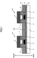
- FIG. 1 is a diagram illustrating a configuration example of a light-emitting structure with leakage reducing function 10 applied to a transmissive LED display according to an embodiment.
- FIG. 1 illustrates a cross-sectional structure of the light-emitting structure with leakage reducing function 10 when the transmissive LED display is viewed from the side, in which the upper part of the figure is the front surface of the display and the lower part of the figure is the back surface of the display.
- two light-emitting structures with leakage reducing function 10 are illustrated in juxtaposition, but actually, more light-emitting structures with leakage reducing function 10 are arranged in an array (see FIGS. 4A to 5 described later).
- one light-emitting structure with leakage reducing function 10 has one set including an anode electrode 2 and a cathode electrode 3 arranged at a predetermined interval on a transparent substrate 1, and an LED 4 arranged between the anode electrode 2 and the cathode electrode 3 and electrically connected to the electrodes.
- two electrode pads 6 are arranged in two contact holes 5 formed in two insulating layers 8 and 9 on the anode electrode 2 and the cathode electrode 3, and the LED 4 is mounted by a conductive adhesive 7 formed on the electrode pads 6.
- An opening 20 in which the anode electrode 2 and the cathode electrode 3 are not arranged is provided between two adjacent light-emitting structures with leakage reducing function 10. Through the opening 20, light is transmittable from the back surface to the front surface of the transmissive LED display, whereby the area behind the transmissive LED display can be seen through from the front side.
- a light-shielding layer 11 is provided for the light-emitting structure configured as described above.
- This light-shielding layer 11 is a light leakage reducing structure.
- the light-shielding layer 11 is arranged in a target region including a region for shielding the optical path in a direction from a portion of the back surface of the LED 4 facing the gap between the anode electrode 2 and the cathode electrode 3 toward the transparent substrate 1.
- the light-shielding layer 11 is arranged in a target region including a region for shielding the optical path and covering the gap between the anode electrode 2 and the cathode electrode 3 on the front side of the gap.
- the light-shielding layer 11 preferably has a high light shielding property so that the light-shielding layer 11 can shield even high-energy light emission.
- the optical density (OD value) which is an index representing the amount of light transmission (transmittance)
- OD value is preferably set to be "3" or more (transmittance is 0.1% or less). This is in consideration of the fact that the standard OD value of the black matrix formed to prevent light leakage and RGB color mixing in the backlight of the liquid crystal display device is set to be approximately "3".
- FIGS. 2A and 2B are diagrams schematically illustrating the light shielding effect of the light-emitting structure with leakage reducing function 10 according to the present embodiment configured as described above in comparison with a conventional light-emitting structure.
- FIG. 2A illustrates a conventional light-emitting structure
- FIG. 2B illustrates the light-emitting structure with leakage reducing function 10 according to the present embodiment.
- FIGS. 2A and 2B when the LED 4 is turned on, light is emitted not only from the front surface but also from the back surface of the LED 4.
- a second insulating layer 9 is formed on the first insulating layer 8 by vapor deposition, sputtering, spin coating, or the like so as to cover the light-shielding layer 11 (step S4).
- the material of the second insulating layer 9 for example, SiNx, SiOx, acrylic resin, or the like can be used. Because the second insulating layer 9 also serves the role of planarization, it is preferable that the film is thicker than the first insulating layer 8.
- a contact hole 5 is formed on the anode electrode 2 and the cathode electrode 3 by a photolithography process and etching (step S5). Further, an electrode pad 6 is formed in the contact hole 5 mainly by a photolithography process, and the electrode pad 6 is electrically connected to the anode electrode 2 and the cathode electrode 3 (step S6).
- Au, Ag, Cu, AgMg, Al, ITO, or the like can be used as the material of the electrode pad 6.
- the light-shielding layer 11 is not arranged between the anode electrode 2 and the cathode electrode 3, and a part of the back surface of the LED 4 is visible from the back surface of the light-emitting structure through a gap between the anode electrode 2 and the cathode electrode 3. Therefore, light emitted from the back surface of the LED 4 in a direction toward the transparent substrate 1 leaks to the back side through a gap between the anode electrode 2 and the cathode electrode 3.
- the light-emitting structure itself is the same as that illustrated in FIG. 4A . That is, one pixel is composed of three sub-pixels having LEDs 4 for each color of RGB, and openings 20 are formed between adjacent sub-pixels, between adjacent pixels, and between lines.
- the light-emitting structures with leakage reducing function 10 are provided for each sub-pixel.
- the light-shielding layer 11 is arranged in a target region covering a gap between the anode electrode 2 and the cathode electrode 3, whereby light leakage to the back surface can be largely reduced.
- the target region in which the light-shielding layer 11 is arranged may have a length, in a direction (direction L in the figure) connecting the anode electrode 2 and the cathode electrode 3, that is greater than or equal to the interval between the anode electrode 2 and the cathode electrode 3.
- a length that does not overlap the adjacent target regions is set as an upper limit. That is, a length in which the light shielding layers 11 adjacent in the direction L in FIG. 4B do not overlap each other is set as an upper limit.
- the length of the light-shielding layer 11 in the L direction may be set to be a length that protrudes from the anode electrode 2 and the cathode electrode 3 into the opening 20
- the width of the light-shielding layer 11 in the W direction may be set to be a width that protrudes from the anode electrode 2 and the cathode electrode 3 into the opening 20, in this case, a part of the opening 20 is shielded by the light-shielding layer 11, which lowers the aperture ratio of the pixel. Therefore, it is desirable that the portion of the light-shielding layer 11 that protrudes from the anode electrode 2 and the cathode electrode 3 into the opening 20 is not too wide.
- FIG. 1 illustrates a configuration in which the target region in which the light-shielding layer 11 is arranged includes a region for shielding the optical path and a region covering the gap between the anode electrode 2 and the cathode electrode 3 on the front side of the gap
- the light-shielding layer 11 may be positioned on any layer in the cross section of the light-emitting structure as long as the region includes the region for shielding the optical path.
- the light-emitting structure to which the light-shielding layer 11 is applied is not limited to that illustrated in FIG. 1 .
- FIGS. 6A to 6D illustrate several modified examples of the light-emitting structure with leakage reducing function provided with the light-shielding layer 11.
- FIG. 6A illustrates a configuration example of a light-emitting structure with leakage reducing function 10A in which the light-shielding layer 11 is arranged in a target region to close the gap between the two electrode pads 6 connected to the anode electrode 2 and the cathode electrode 3 in the light-emitting structure in which the electrode pad 6 is made lower in height than the light-emitting structure with leakage reducing function 10 illustrated in FIG. 1 and the second insulating layer 9 is eliminated.
- the target region in which the light-shielding layer 11 is arranged is a region shielding the optical path and a region to cover the gap between the anode electrode 2 and the cathode electrode 3 on the front side of the gap.
- FIG. 6B illustrates a configuration example of a light-emitting structure with leakage reducing function 10B in which the light-shielding layer 11 is arranged in a target region to close the gap between the anode electrode 2 and the cathode electrode 3 in the light-emitting structure in which the contact hole 5, the electrode pad 6, and the insulating layers 8 and 9 illustrated in the light-emitting structure with leakage reducing function 10 illustrated in FIG. 1 are eliminated and the conductive adhesive 7 is directly formed on the anode electrode 2 and the cathode electrode 3 to mount the LED 4.
- the light-shielding layer 11 may be arranged in a target region to close the gap between the anode electrode 2 and the cathode electrode 3.
- FIG. 6C illustrates a configuration example of a light-emitting structure with leakage reducing function 10C in which the light-shielding layer 11 is arranged on the back surface of the transparent substrate 1 in the light-emitting structure similar to that illustrated in FIG. 6B .
- the target region in which the light-shielding layer 11 is arranged includes a region for shielding the optical path and a region covering the gap between the anode electrode 2 and the cathode electrode 3 on the back side of the gap.
- the light-shielding layer 11 may be arranged on the back side of the transparent substrate 1.
- FIG. 6D illustrates a configuration example of a light-emitting structure with leakage reducing function 10D in which the light-shielding layer 11 is arranged on the back side of the LED 4 in the light-emitting structure similar to that in FIG. 6B .
- the light-shielding layer 11 may be arranged on the back side of the LED 4.
- the light-shielding layer 11 is arranged in a target region including a region shielding the optical path, on the optical path in the direction from the back side of the LED 4 facing the gap between the anode electrode 2 and the cathode electrode 3 toward the transparent substrate 1.
- the light-emitting structure with leakage reducing function of the present embodiments can be applied to any transmission type display having a structure in which the light emitted from the light source leaks through the gap between the electrodes.
Landscapes
- Physics & Mathematics (AREA)
- Nonlinear Science (AREA)
- Mathematical Physics (AREA)
- Chemical & Material Sciences (AREA)
- Crystallography & Structural Chemistry (AREA)
- General Physics & Mathematics (AREA)
- Optics & Photonics (AREA)
- Geometry (AREA)
- Devices For Indicating Variable Information By Combining Individual Elements (AREA)
- Led Device Packages (AREA)
Abstract
A transmission type display is provided, wherein a plurality of light sources are arranged between a plurality of sets of electrodes arranged in an array on a transparent substrate, and a plurality of openings where the electrodes are not arranged are provided, so that light is transmittable through the plurality of openings. A light shielding layer is arranged in a target region including a region shielding an optical path in a direction from a portion of a back surface of the light source facing a gap between the electrodes toward the transparent substrate.
Description
- The present invention relates to a transmission type display, and is particularly suitable for use in a transmission type display in which a plurality of light sources are arranged between a plurality of sets of electrodes arranged in an array on a transparent substrate, and a plurality of openings are provided in which no electrodes are arranged so that light is transmittable through the plurality of openings.
- Conventionally, unlike a general display, a transmission type display in which the area behind the display can be seen through, is known. In the transmission type display, a plurality of light sources are arranged in an array on a transparent substrate and a plurality of openings, where electrodes and the like are not arranged, are provided so that light is transmittable from the back side to the front side of the display through the openings. The ratio of the area of the openings occupying the area of one pixel is referred to as the aperture ratio, and the larger the aperture ratio, the more light from the background can be taken in, and the display can be almost transparent in appearance.
- There are various types of transmission type displays, and among them, a transmissive LED display is expected to be applied to various applications because it can achieve a high transmittance of 70% or more. When a transmissive LED display is constructed, it is preferable to use a technology referred to as micro-LED, which is made by miniaturizing LEDs used as light sources and arranging them in an array. A display using micro-LED is disclosed in
JP 2021-052156 A JP 2022-093393 A WO 2023-127585 A , for example. -
FIGS. 7A and 7B are simplified diagrams illustrating the structure of the light-emitting portion of the transmissive LED display.FIG. 7A illustrates a state in which the light-emitting portion of the transmissive LED display is viewed from the front side, andFIG. 7B illustrates a state in which the light-emitting portion of the transmissive LED display is viewed from the back side. As illustrated inFIGS. 7A and 7B , a plurality ofLEDs 101 are arranged in an array, and a plurality ofopenings 102 are arranged in an array so as to be adjacent to the plurality ofLEDs 101. The plurality ofLEDs 101 are each arranged between ananode electrode 103 and acathode electrode 104. - However, in the transmissive LED display configured in this way, there has been a problem that light emitted from the
LED 101 for projecting information on the front side leaks to the back side through a gap between theanode electrode 103 and thecathode electrode 104. That is, as illustrated inFIG. 7B , when the transmissive LED display is viewed from the back side, a part of theLED 101 is visible through a gap between theanode electrode 103 and thecathode electrode 104. In the transmissive LED display, not only the substrate arranged on the front side of theLED 101 is made of a transparent substrate, but also the substrate arranged on the back side of theLED 101 is made of a transparent substrate. Therefore, when theLED 101 is turned on, light leaks from the back side of theLED 101 to the back side of the display through a gap between theelectrodes - An object of the present invention is to reduce light emitted when a light source is turned on from leaking to the back surface of the display in a transmission type display.
- The present disclosure relates to a transmission type display according to the appended claims. Embodiments are disclosed in the dependent claims. According to an embodiment, in a transmission type display, a plurality of light sources are arranged between a plurality of sets of electrodes arranged in an array on a transparent substrate, and a plurality of openings where the electrodes are not arranged are provided, so that light is transmittable through the plurality of openings, wherein a light shielding layer is arranged in a target region including a region shielding an optical path in a direction from a portion of a back surface of the light source facing a gap between the electrodes toward the transparent substrate.
- Other objects and further features of the present invention will be apparent from the following detailed description when read in conjunction with the accompanying drawings, in which:
-
FIG. 1 is a diagram illustrating a configuration example of a light-emitting structure with leakage reducing function applied to a transmissive LED display according to an embodiment; -
FIG. 2A is a diagram schematically illustrating a conventional light-emitting structure, andFIG. 2B is a diagram schematically illustrating the light shielding effect of the light-emitting structure with leakage reducing function according to an embodiment; -
FIG. 3 is a diagram schematically illustrating an example of a manufacturing process of the light-emitting structure with leakage reducing function according to an embodiment; -
FIG. 4A is a diagram schematically illustrating an example of an array arrangement of a conventional light-emitting structure, andFIG. 4B is a diagram schematically illustrating an example of an array arrangement of the light-emitting structures with leakage reducing function according to an embodiment; -
FIG. 5 is a diagram schematically illustrating another example of an array arrangement of a light-emitting structure with leakage reducing function according to an embodiment; -
FIGS. 6A to 6D are diagrams illustrating a modified example of a light-emitting structure with leakage reducing function provided with a light-shielding layer according to an embodiment; and -
FIGS. 7A and 7B are diagrams illustrating the structure of a light-emitting portion of a transmissive LED display. - According to aspects of the present invention configured as described above, in the transmission type display, the light, which is emitted from the back surface of the light source in a direction toward the transparent substrate when the light source is turned on, is shielded by the light shielding layer, and, therefore, leakage of light emitted from the light source to the back surface of the display can be reduced.
- Hereinafter, embodiments of the present invention will be described with reference to the drawings. The transmission type display of the present embodiment is a transmission type display in which a plurality of light sources are arranged between a plurality of sets of electrodes arranged in an array on a transparent substrate, and a plurality of openings in which no electrodes are arranged are provided so that light is transmittable through the plurality of openings. As a result, the background light is transmitted from the back surface of the display to the front surface, and the area behind the display is seen through from the front side.
- In the present embodiment, a structure for reducing light leakage to the back surface is applied to the light-emitting structure of a transmissive LED display using a micro-LED element as an example of a light source. In the following description, the term "light-emitting structure with leakage reducing function" refers to the light-emitting structure including the light leakage reducing structure of the present embodiment, and is distinguished from the light-emitting structure not including the light leakage reducing structure.
-
FIG. 1 is a diagram illustrating a configuration example of a light-emitting structure withleakage reducing function 10 applied to a transmissive LED display according to an embodiment.FIG. 1 illustrates a cross-sectional structure of the light-emitting structure withleakage reducing function 10 when the transmissive LED display is viewed from the side, in which the upper part of the figure is the front surface of the display and the lower part of the figure is the back surface of the display. InFIG. 1 , two light-emitting structures withleakage reducing function 10 are illustrated in juxtaposition, but actually, more light-emitting structures withleakage reducing function 10 are arranged in an array (seeFIGS. 4A to 5 described later). - As illustrated in
FIG. 1 , one light-emitting structure withleakage reducing function 10 has one set including ananode electrode 2 and acathode electrode 3 arranged at a predetermined interval on atransparent substrate 1, and anLED 4 arranged between theanode electrode 2 and thecathode electrode 3 and electrically connected to the electrodes. In the example ofFIG. 1 , twoelectrode pads 6 are arranged in twocontact holes 5 formed in twoinsulating layers anode electrode 2 and thecathode electrode 3, and theLED 4 is mounted by aconductive adhesive 7 formed on theelectrode pads 6. - An opening 20 in which the
anode electrode 2 and thecathode electrode 3 are not arranged is provided between two adjacent light-emitting structures withleakage reducing function 10. Through theopening 20, light is transmittable from the back surface to the front surface of the transmissive LED display, whereby the area behind the transmissive LED display can be seen through from the front side. - In the present embodiment, a light-
shielding layer 11 is provided for the light-emitting structure configured as described above. This light-shielding layer 11 is a light leakage reducing structure. The light-shielding layer 11 is arranged in a target region including a region for shielding the optical path in a direction from a portion of the back surface of theLED 4 facing the gap between theanode electrode 2 and thecathode electrode 3 toward thetransparent substrate 1. In the example ofFIG. 1 , the light-shielding layer 11 is arranged in a target region including a region for shielding the optical path and covering the gap between theanode electrode 2 and thecathode electrode 3 on the front side of the gap. - The light-
shielding layer 11 preferably has a high light shielding property so that the light-shielding layer 11 can shield even high-energy light emission. For example, the optical density (OD value), which is an index representing the amount of light transmission (transmittance), is preferably set to be "3" or more (transmittance is 0.1% or less). This is in consideration of the fact that the standard OD value of the black matrix formed to prevent light leakage and RGB color mixing in the backlight of the liquid crystal display device is set to be approximately "3". -
FIGS. 2A and 2B are diagrams schematically illustrating the light shielding effect of the light-emitting structure withleakage reducing function 10 according to the present embodiment configured as described above in comparison with a conventional light-emitting structure.FIG. 2A illustrates a conventional light-emitting structure, andFIG. 2B illustrates the light-emitting structure withleakage reducing function 10 according to the present embodiment. As illustrated inFIGS. 2A and 2B , when theLED 4 is turned on, light is emitted not only from the front surface but also from the back surface of theLED 4. - In the case of the conventional light-emitting structure illustrated in
FIG. 2A , light emitted from the back surface of theLED 4 in the direction toward thetransparent substrate 1 leaks through the gap between theanode electrode 2 and thecathode electrode 3 to the back surface of thetransparent substrate 1. In contrast, in the case of the light-emitting structure withleakage reducing function 10 according to the present embodiment illustrated inFIG. 2B , light emitted from the back surface of theLED 4 in the direction toward thetransparent substrate 1 is shielded by the light-shielding layer 11 arranged so as to cover the gap between theanode electrode 2 and thecathode electrode 3. Therefore, light emitted from the back surface of theLED 4 is substantially prevented or prevented from leaking through the gap between theanode electrode 2 and thecathode electrode 3 to the back surface of thetransparent substrate 1. -
FIG. 3 is a diagram illustrating an example of a manufacturing process of the light-emitting structure withleakage reducing function 10 illustrated inFIG. 1 . Note that the materials and steps described below are only examples, and are not limited thereto. - First, the
anode electrode 2 and thecathode electrode 3 are formed on the transparent substrate 1 (step S1). As the materials of theanode electrode 2 and thecathode electrode 3, for example, Au, Ag, Cu, AgMg, Al, ITO, and the like can be used. As the process, a photolithography process is mainly used. The arrangement of theanode electrode 2 and thecathode electrode 3 is not limited to a simple matrix or an active matrix, but may be an irregular arrangement. - Next, a first insulating
layer 8 is formed on thetransparent substrate 1 so as to cover theanode electrode 2 and thecathode electrode 3 by vapor deposition, sputtering, or spin coating (step S2). As the material of the first insulatinglayer 8, for example, SiNx, SiOx, acrylic resin, or the like can be used. - Next, the light-
shielding layer 11 is formed on the first insulatinglayer 8 in a target region covering the gap between theanode electrode 2 and the cathode electrode 3 (step S3). For example, a light-shielding material is applied on the first insulatinglayer 8 by vapor deposition or spin coating, and the light-shielding layer 11 is formed on the target region covering the gap between theanode electrode 2 and thecathode electrode 3 by a photolithography process. As the light-shielding material, for example, a photosensitive resin containing a black pigment, chromium oxide, or the like can be used. - Next, a second
insulating layer 9 is formed on the first insulatinglayer 8 by vapor deposition, sputtering, spin coating, or the like so as to cover the light-shielding layer 11 (step S4). As the material of the second insulatinglayer 9, for example, SiNx, SiOx, acrylic resin, or the like can be used. Because the second insulatinglayer 9 also serves the role of planarization, it is preferable that the film is thicker than the first insulatinglayer 8. - Next, a
contact hole 5 is formed on theanode electrode 2 and thecathode electrode 3 by a photolithography process and etching (step S5). Further, anelectrode pad 6 is formed in thecontact hole 5 mainly by a photolithography process, and theelectrode pad 6 is electrically connected to theanode electrode 2 and the cathode electrode 3 (step S6). For example, Au, Ag, Cu, AgMg, Al, ITO, or the like can be used as the material of theelectrode pad 6. - Finally, after the
conductive adhesive 7 is formed on theelectrode pad 6, theLED 4 is mounted (step S7). As theconductive adhesive 7, for example, solder, ACF (anisotropic conductive film), or a material in which conductive particles are dispersed in resin can be used. After theLED 4 is placed in the correct position, mounting is performed by reflow soldering in the case of using solder, and by pressurization and heating in the case of using other materials, to solidify theLED 4. -
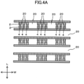
FIGS. 4A and4B is a diagram schematically illustrating an example of an array arrangement of the light-emitting structures withleakage reducing function 10 in comparison with an array arrangement of a conventional light-emitting structure.FIG. 4A is an array arrangement of a conventional light-emitting structure, and illustrates a state in which the light-emitting structure is viewed from the back side.FIG. 4B is an array arrangement of the light-emitting structures withleakage reducing function 10, and illustrates a state in which the light-emitting structures withleakage reducing function 10 are viewed from the back side. - In the conventional light-emitting structure array arrangement illustrated in
FIG. 4A , one pixel is composed of threesub-pixels having LEDs 4 for each of the RGB colors (red LED, green LED, and blue LED), and a light-emitting structure is provided for each sub-pixel. Further,openings 20 are formed between adjacent sub-pixels and between adjacent pixels, respectively. InFIG. 4A , an electrode pattern is used when a plurality ofLEDs 4 arranged in a line shape are collectively lit (lit all at once), and theopenings 20 are formed between lines. The light-shielding layer 11 is not arranged between theanode electrode 2 and thecathode electrode 3, and a part of the back surface of theLED 4 is visible from the back surface of the light-emitting structure through a gap between theanode electrode 2 and thecathode electrode 3. Therefore, light emitted from the back surface of theLED 4 in a direction toward thetransparent substrate 1 leaks to the back side through a gap between theanode electrode 2 and thecathode electrode 3. - In the array arrangement of the present embodiment illustrated in
FIG. 4B , the light-emitting structure itself is the same as that illustrated inFIG. 4A . That is, one pixel is composed of threesub-pixels having LEDs 4 for each color of RGB, andopenings 20 are formed between adjacent sub-pixels, between adjacent pixels, and between lines. In the case ofFIG. 4B , the light-emitting structures withleakage reducing function 10 are provided for each sub-pixel. In each light-emitting structure withleakage reducing function 10, the light-shielding layer 11 is arranged in a target region covering a gap between theanode electrode 2 and thecathode electrode 3, whereby light leakage to the back surface can be largely reduced. - Note that although an example of a configuration with a sub-pixel in which three
RGB LEDs 4 are arranged in one pixel has been described here, a configuration without a sub-pixel in which oneLED 4 is arranged in one pixel may be used. - Here, in order to enhance the effect of reducing light leakage, the target region in which the light-
shielding layer 11 is arranged may have a length, in a direction (direction L in the figure) connecting theanode electrode 2 and thecathode electrode 3, that is greater than or equal to the interval between theanode electrode 2 and thecathode electrode 3. However, a length that does not overlap the adjacent target regions is set as an upper limit. That is, a length in which the light shielding layers 11 adjacent in the direction L inFIG. 4B do not overlap each other is set as an upper limit. Further, in the target region in which the light-shielding layer 11 is arranged, a width in a direction (direction W in the figure) orthogonal to the direction connecting theanode electrode 2 and thecathode electrode 3 may be set as a width greater than or equal to the width of theanode electrode 2 and thecathode electrode 3 or the width of theLED 4, whichever is narrower. However, a width that does not overlap the adjacent target regions is set as an upper limit. That is, a width in which the light shielding layers 11 adjacent in the direction W inFIG. 4B do not overlap each other is set as an upper limit. - Although the length of the light-
shielding layer 11 in the L direction may be set to be a length that protrudes from theanode electrode 2 and thecathode electrode 3 into theopening 20, and the width of the light-shielding layer 11 in the W direction may be set to be a width that protrudes from theanode electrode 2 and thecathode electrode 3 into theopening 20, in this case, a part of theopening 20 is shielded by the light-shielding layer 11, which lowers the aperture ratio of the pixel. Therefore, it is desirable that the portion of the light-shielding layer 11 that protrudes from theanode electrode 2 and thecathode electrode 3 into theopening 20 is not too wide. Regardless of the length or width of the light-shielding layer 11, it is preferable that the target region in which the light-shielding layer 11 is arranged is a region that does not protrude from theanode electrode 2 and thecathode electrode 3 into theopening 20. - Although
FIGS. 4A and4B illustrate an electrode pattern in the case where a plurality ofLEDs 4 arranged in a line shape are lit all at once, it is also possible to apply the light-emitting structure withleakage reducing function 10 of the present embodiment to other electrode patterns. For example, it is also possible to apply this to the case where a plurality ofLEDs 4 are arranged in a matrix as illustrated inFIG. 5 . In the example of the array arrangement illustrated inFIG. 5 , theanode electrode 2 andcathode electrode 3 protruding like branches from theelectrodes LEDs 4. Also in this case, the light-shielding layer 11 is arranged in a gap between theanode electrode 2 and thecathode electrode 3. - Although
FIG. 1 illustrates a configuration in which the target region in which the light-shielding layer 11 is arranged includes a region for shielding the optical path and a region covering the gap between theanode electrode 2 and thecathode electrode 3 on the front side of the gap, the light-shielding layer 11 may be positioned on any layer in the cross section of the light-emitting structure as long as the region includes the region for shielding the optical path. Further, the light-emitting structure to which the light-shielding layer 11 is applied is not limited to that illustrated inFIG. 1 .FIGS. 6A to 6D illustrate several modified examples of the light-emitting structure with leakage reducing function provided with the light-shielding layer 11. -
FIG. 6A illustrates a configuration example of a light-emitting structure withleakage reducing function 10A in which the light-shielding layer 11 is arranged in a target region to close the gap between the twoelectrode pads 6 connected to theanode electrode 2 and thecathode electrode 3 in the light-emitting structure in which theelectrode pad 6 is made lower in height than the light-emitting structure withleakage reducing function 10 illustrated inFIG. 1 and the second insulatinglayer 9 is eliminated. Also in this configuration example, the target region in which the light-shielding layer 11 is arranged is a region shielding the optical path and a region to cover the gap between theanode electrode 2 and thecathode electrode 3 on the front side of the gap. -
FIG. 6B illustrates a configuration example of a light-emitting structure withleakage reducing function 10B in which the light-shielding layer 11 is arranged in a target region to close the gap between theanode electrode 2 and thecathode electrode 3 in the light-emitting structure in which thecontact hole 5, theelectrode pad 6, and the insulatinglayers leakage reducing function 10 illustrated inFIG. 1 are eliminated and theconductive adhesive 7 is directly formed on theanode electrode 2 and thecathode electrode 3 to mount theLED 4. In the light-emitting structure similar toFIG. 1 andFIG. 6A , the light-shielding layer 11 may be arranged in a target region to close the gap between theanode electrode 2 and thecathode electrode 3. -
FIG. 6C illustrates a configuration example of a light-emitting structure withleakage reducing function 10C in which the light-shielding layer 11 is arranged on the back surface of thetransparent substrate 1 in the light-emitting structure similar to that illustrated inFIG. 6B . In this case, the target region in which the light-shielding layer 11 is arranged includes a region for shielding the optical path and a region covering the gap between theanode electrode 2 and thecathode electrode 3 on the back side of the gap. In the light-emitting structure similar to that inFIGS. 1 and6A , the light-shielding layer 11 may be arranged on the back side of thetransparent substrate 1. -
FIG. 6D illustrates a configuration example of a light-emitting structure withleakage reducing function 10D in which the light-shielding layer 11 is arranged on the back side of theLED 4 in the light-emitting structure similar to that inFIG. 6B . In the light-emitting structure similar to that inFIGS. 1 and6A , the light-shielding layer 11 may be arranged on the back side of theLED 4. - As described above in detail, in the present embodiments, in the light-emitting structure of a transmissive LED display using micro-LED elements, the light-
shielding layer 11 is arranged in a target region including a region shielding the optical path, on the optical path in the direction from the back side of theLED 4 facing the gap between theanode electrode 2 and thecathode electrode 3 toward thetransparent substrate 1. Thus, when theLED 4 is turned on, the light emitted in the direction from the back side of theLED 4 toward thetransparent substrate 1 is shielded by the light-shielding layer 11, so that the light emitted from theLED 4 can be substantially prevented or prevented from leaking to the back side of the display. - Although the structure of applying the light-
shielding layer 11 to the transmissive LED display using micro-LED elements has been described in the above embodiments, the light-emitting structure with leakage reducing function of the present embodiments can be applied to any transmission type display having a structure in which the light emitted from the light source leaks through the gap between the electrodes. - All of the above embodiments merely indicate examples of embodiments of the present invention, and the technical scope of the present invention should not be interpreted as being limited. That is, the present invention can be practiced in various forms without departing from the scope of the claims.
Claims (7)
- A transmission type display, whereina plurality of light sources are arranged between a plurality of sets of electrodes arranged in an array on a transparent substrate, and a plurality of openings where the electrodes are not arranged are provided, so that light is transmittable through the plurality of openings, whereina light shielding layer is arranged in a target region including a region shielding an optical path in a direction from a portion of a back surface of the light source facing a gap between the electrodes toward the transparent substrate.
- The transmission type display according to claim 1, wherein the target region includes the region shielding the optical path and is a region covering the gap between the electrodes.
- The transmission type display according to claim 1 or 2, wherein the target region has a length in a direction connecting the electrodes that is greater than or equal to an interval between the electrodes and that does not overlap with an adjacent target region.
- The transmission type display according to one of claims 1 - 3, wherein the target region has a width in a direction orthogonal to the direction connecting the electrodes that is greater than or equal to a width of the electrode or the light source, whichever is narrower and that does not overlap with an adjacent target region.
- The transmission type display according to one of claims 1 - 4, wherein the target region includes the region shielding the optical path and is a region that closes the gap between the electrodes.
- The transmission type display according to one of claims 1 - 5, wherein the light shielding layer has an optical density of three or more.
- The transmission type display according to one of claims 1 - 6, wherein a micro-LED element is used as the light source.
Applications Claiming Priority (1)
| Application Number | Priority Date | Filing Date | Title |
|---|---|---|---|
| JP2023199050A JP2025085281A (en) | 2023-11-24 | 2023-11-24 | Transmissive Display |
Publications (1)
| Publication Number | Publication Date |
|---|---|
| EP4561306A1 true EP4561306A1 (en) | 2025-05-28 |
Family
ID=93563376
Family Applications (1)
| Application Number | Title | Priority Date | Filing Date |
|---|---|---|---|
| EP24213373.4A Pending EP4561306A1 (en) | 2023-11-24 | 2024-11-15 | Transmission type display |
Country Status (4)
| Country | Link |
|---|---|
| US (1) | US20250174607A1 (en) |
| EP (1) | EP4561306A1 (en) |
| JP (1) | JP2025085281A (en) |
| CN (1) | CN120044724A (en) |
Citations (6)
| Publication number | Priority date | Publication date | Assignee | Title |
|---|---|---|---|---|
| JP2013073868A (en) * | 2011-09-29 | 2013-04-22 | Japan Display West Inc | Lighting unit, and display device |
| JP2013110052A (en) * | 2011-11-24 | 2013-06-06 | Japan Display West Inc | Lighting device and display device |
| JP2021052156A (en) | 2019-09-20 | 2021-04-01 | 東貝光電科技股▲ふん▼有限公司Unity Opto Technology Co.,Ltd. | Method for manufacturing micro led panel, and micro led panel |
| US20210399042A1 (en) * | 2018-08-15 | 2021-12-23 | PlayNitride Display Co., Ltd. | Transparent display panel |
| JP2022093393A (en) | 2020-10-02 | 2022-06-23 | 伯仁 ▲呉▼ | Display panel and display panel manufacturing method |
| WO2023127585A1 (en) | 2021-12-28 | 2023-07-06 | 株式会社東海理化電機製作所 | Display device manufacturing jig, display device manufacturing method, display device manufactured using display device manufacturing jig, and display device manufactured using display device manufacturing method |
-
2023
- 2023-11-24 JP JP2023199050A patent/JP2025085281A/en active Pending
-
2024
- 2024-11-15 EP EP24213373.4A patent/EP4561306A1/en active Pending
- 2024-11-19 CN CN202411652396.8A patent/CN120044724A/en active Pending
- 2024-11-19 US US18/952,282 patent/US20250174607A1/en active Pending
Patent Citations (6)
| Publication number | Priority date | Publication date | Assignee | Title |
|---|---|---|---|---|
| JP2013073868A (en) * | 2011-09-29 | 2013-04-22 | Japan Display West Inc | Lighting unit, and display device |
| JP2013110052A (en) * | 2011-11-24 | 2013-06-06 | Japan Display West Inc | Lighting device and display device |
| US20210399042A1 (en) * | 2018-08-15 | 2021-12-23 | PlayNitride Display Co., Ltd. | Transparent display panel |
| JP2021052156A (en) | 2019-09-20 | 2021-04-01 | 東貝光電科技股▲ふん▼有限公司Unity Opto Technology Co.,Ltd. | Method for manufacturing micro led panel, and micro led panel |
| JP2022093393A (en) | 2020-10-02 | 2022-06-23 | 伯仁 ▲呉▼ | Display panel and display panel manufacturing method |
| WO2023127585A1 (en) | 2021-12-28 | 2023-07-06 | 株式会社東海理化電機製作所 | Display device manufacturing jig, display device manufacturing method, display device manufactured using display device manufacturing jig, and display device manufactured using display device manufacturing method |
Also Published As
| Publication number | Publication date |
|---|---|
| CN120044724A (en) | 2025-05-27 |
| US20250174607A1 (en) | 2025-05-29 |
| JP2025085281A (en) | 2025-06-05 |
Similar Documents
| Publication | Publication Date | Title |
|---|---|---|
| US9357612B2 (en) | Display device | |
| CN112820759B (en) | Transparent display panel and transparent display device including the same | |
| TWI615963B (en) | Organic light emitting display device and method of manufacturing same | |
| CN112310322A (en) | Display panel and display device | |
| CN212460249U (en) | Display module and display device | |
| US20210109389A1 (en) | Display device | |
| US20030067569A1 (en) | Liquid crystal display panel having light impermeable layer with alignment marks | |
| CN115720474A (en) | Display panel and display device | |
| CN112764260B (en) | Liquid crystal display panel and liquid crystal display device | |
| US7713596B2 (en) | Light shading structure, and color filter substrate, active device array substrate, liquid crystal display panel thereof | |
| WO2022257167A1 (en) | Display panel and electronic device | |
| US20250174607A1 (en) | Transmission type display | |
| KR100763061B1 (en) | Display device | |
| US11187935B2 (en) | Display panel and display device | |
| CN117729801A (en) | Display panels and display devices | |
| CN116736595A (en) | Display panel and display device | |
| CN119907530B (en) | Display panel and display device | |
| CN101369070B (en) | Display apparatus | |
| CN223391631U (en) | Display panel and display device | |
| KR102428392B1 (en) | Organic Light Emitting Diode Display Device | |
| CN213069421U (en) | Display panel and display device | |
| US20250331392A1 (en) | Display panel and display device | |
| KR20260041426A (en) | Transparent display apparatus | |
| CN119233699A (en) | Display panel, preparation method thereof and VR device | |
| CN116782715A (en) | Display panel and display device |
Legal Events
| Date | Code | Title | Description |
|---|---|---|---|
| PUAI | Public reference made under article 153(3) epc to a published international application that has entered the european phase |
Free format text: ORIGINAL CODE: 0009012 |
|
| STAA | Information on the status of an ep patent application or granted ep patent |
Free format text: STATUS: THE APPLICATION HAS BEEN PUBLISHED |
|
| AK | Designated contracting states |
Kind code of ref document: A1 Designated state(s): AL AT BE BG CH CY CZ DE DK EE ES FI FR GB GR HR HU IE IS IT LI LT LU LV MC ME MK MT NL NO PL PT RO RS SE SI SK SM TR |
|
| STAA | Information on the status of an ep patent application or granted ep patent |
Free format text: STATUS: REQUEST FOR EXAMINATION WAS MADE |
|
| 17P | Request for examination filed |
Effective date: 20251013 |