EP4557895A1 - Clips serving as vertical interconnect - Google Patents
Clips serving as vertical interconnect Download PDFInfo
- Publication number
- EP4557895A1 EP4557895A1 EP24212728.0A EP24212728A EP4557895A1 EP 4557895 A1 EP4557895 A1 EP 4557895A1 EP 24212728 A EP24212728 A EP 24212728A EP 4557895 A1 EP4557895 A1 EP 4557895A1
- Authority
- EP
- European Patent Office
- Prior art keywords
- clip
- circuit board
- dielectric body
- electronic
- clips
- Prior art date
- Legal status (The legal status is an assumption and is not a legal conclusion. Google has not performed a legal analysis and makes no representation as to the accuracy of the status listed.)
- Pending
Links
Images



Classifications
-
- H—ELECTRICITY
- H05—ELECTRIC TECHNIQUES NOT OTHERWISE PROVIDED FOR
- H05K—PRINTED CIRCUITS; CASINGS OR CONSTRUCTIONAL DETAILS OF ELECTRIC APPARATUS; MANUFACTURE OF ASSEMBLAGES OF ELECTRICAL COMPONENTS
- H05K1/00—Printed circuits
- H05K1/02—Details
- H05K1/14—Structural association of two or more printed circuits
- H05K1/145—Arrangements wherein electric components are disposed between and simultaneously connected to two planar printed circuit boards, e.g. Cordwood modules
-
- H—ELECTRICITY
- H05—ELECTRIC TECHNIQUES NOT OTHERWISE PROVIDED FOR
- H05K—PRINTED CIRCUITS; CASINGS OR CONSTRUCTIONAL DETAILS OF ELECTRIC APPARATUS; MANUFACTURE OF ASSEMBLAGES OF ELECTRICAL COMPONENTS
- H05K1/00—Printed circuits
- H05K1/02—Details
- H05K1/0213—Electrical arrangements not otherwise provided for
-
- H—ELECTRICITY
- H01—ELECTRIC ELEMENTS
- H01R—ELECTRICALLY-CONDUCTIVE CONNECTIONS; STRUCTURAL ASSOCIATIONS OF A PLURALITY OF MUTUALLY-INSULATED ELECTRICAL CONNECTING ELEMENTS; COUPLING DEVICES; CURRENT COLLECTORS
- H01R12/00—Structural associations of a plurality of mutually-insulated electrical connecting elements, specially adapted for printed circuits, e.g. printed circuit boards [PCB], flat or ribbon cables, or like generally planar structures, e.g. terminal strips, terminal blocks; Coupling devices specially adapted for printed circuits, flat or ribbon cables, or like generally planar structures; Terminals specially adapted for contact with, or insertion into, printed circuits, flat or ribbon cables, or like generally planar structures
- H01R12/70—Coupling devices
- H01R12/71—Coupling devices for rigid printing circuits or like structures
-
- H—ELECTRICITY
- H01—ELECTRIC ELEMENTS
- H01F—MAGNETS; INDUCTANCES; TRANSFORMERS; SELECTION OF MATERIALS FOR THEIR MAGNETIC PROPERTIES
- H01F17/00—Fixed inductances of the signal type
- H01F17/04—Fixed inductances of the signal type with magnetic core
-
- H—ELECTRICITY
- H01—ELECTRIC ELEMENTS
- H01F—MAGNETS; INDUCTANCES; TRANSFORMERS; SELECTION OF MATERIALS FOR THEIR MAGNETIC PROPERTIES
- H01F27/00—Details of transformers or inductances, in general
- H01F27/06—Mounting, supporting or suspending transformers, reactors or choke coils not being of the signal type
-
- H—ELECTRICITY
- H01—ELECTRIC ELEMENTS
- H01F—MAGNETS; INDUCTANCES; TRANSFORMERS; SELECTION OF MATERIALS FOR THEIR MAGNETIC PROPERTIES
- H01F27/00—Details of transformers or inductances, in general
- H01F27/28—Coils; Windings; Conductive connections
- H01F27/2847—Sheets; Strips
- H01F27/2852—Construction of conductive connections, of leads
-
- H—ELECTRICITY
- H01—ELECTRIC ELEMENTS
- H01F—MAGNETS; INDUCTANCES; TRANSFORMERS; SELECTION OF MATERIALS FOR THEIR MAGNETIC PROPERTIES
- H01F27/00—Details of transformers or inductances, in general
- H01F27/28—Coils; Windings; Conductive connections
- H01F27/29—Terminals; Tapping arrangements for signal inductances
- H01F27/292—Surface mounted devices
-
- H—ELECTRICITY
- H01—ELECTRIC ELEMENTS
- H01F—MAGNETS; INDUCTANCES; TRANSFORMERS; SELECTION OF MATERIALS FOR THEIR MAGNETIC PROPERTIES
- H01F27/00—Details of transformers or inductances, in general
- H01F27/28—Coils; Windings; Conductive connections
- H01F27/30—Fastening or clamping coils, windings, or parts thereof together; Fastening or mounting coils or windings on core, casing, or other support
- H01F27/306—Fastening or mounting coils or windings on core, casing or other support
-
- H—ELECTRICITY
- H01—ELECTRIC ELEMENTS
- H01R—ELECTRICALLY-CONDUCTIVE CONNECTIONS; STRUCTURAL ASSOCIATIONS OF A PLURALITY OF MUTUALLY-INSULATED ELECTRICAL CONNECTING ELEMENTS; COUPLING DEVICES; CURRENT COLLECTORS
- H01R12/00—Structural associations of a plurality of mutually-insulated electrical connecting elements, specially adapted for printed circuits, e.g. printed circuit boards [PCB], flat or ribbon cables, or like generally planar structures, e.g. terminal strips, terminal blocks; Coupling devices specially adapted for printed circuits, flat or ribbon cables, or like generally planar structures; Terminals specially adapted for contact with, or insertion into, printed circuits, flat or ribbon cables, or like generally planar structures
- H01R12/70—Coupling devices
- H01R12/71—Coupling devices for rigid printing circuits or like structures
- H01R12/72—Coupling devices for rigid printing circuits or like structures coupling with the edge of the rigid printed circuits or like structures
- H01R12/73—Coupling devices for rigid printing circuits or like structures coupling with the edge of the rigid printed circuits or like structures connecting to other rigid printed circuits or like structures
-
- H—ELECTRICITY
- H01—ELECTRIC ELEMENTS
- H01R—ELECTRICALLY-CONDUCTIVE CONNECTIONS; STRUCTURAL ASSOCIATIONS OF A PLURALITY OF MUTUALLY-INSULATED ELECTRICAL CONNECTING ELEMENTS; COUPLING DEVICES; CURRENT COLLECTORS
- H01R13/00—Details of coupling devices of the kinds covered by groups H01R12/70 or H01R24/00 - H01R33/00
- H01R13/02—Contact members
-
- H—ELECTRICITY
- H01—ELECTRIC ELEMENTS
- H01R—ELECTRICALLY-CONDUCTIVE CONNECTIONS; STRUCTURAL ASSOCIATIONS OF A PLURALITY OF MUTUALLY-INSULATED ELECTRICAL CONNECTING ELEMENTS; COUPLING DEVICES; CURRENT COLLECTORS
- H01R43/00—Apparatus or processes specially adapted for manufacturing, assembling, maintaining, or repairing of line connectors or current collectors or for joining electric conductors
- H01R43/027—Apparatus or processes specially adapted for manufacturing, assembling, maintaining, or repairing of line connectors or current collectors or for joining electric conductors for connecting conductors by clips
-
- H—ELECTRICITY
- H05—ELECTRIC TECHNIQUES NOT OTHERWISE PROVIDED FOR
- H05K—PRINTED CIRCUITS; CASINGS OR CONSTRUCTIONAL DETAILS OF ELECTRIC APPARATUS; MANUFACTURE OF ASSEMBLAGES OF ELECTRICAL COMPONENTS
- H05K1/00—Printed circuits
- H05K1/02—Details
- H05K1/14—Structural association of two or more printed circuits
- H05K1/144—Stacked arrangements of planar printed circuit boards
-
- H—ELECTRICITY
- H01—ELECTRIC ELEMENTS
- H01F—MAGNETS; INDUCTANCES; TRANSFORMERS; SELECTION OF MATERIALS FOR THEIR MAGNETIC PROPERTIES
- H01F27/00—Details of transformers or inductances, in general
- H01F27/06—Mounting, supporting or suspending transformers, reactors or choke coils not being of the signal type
- H01F2027/065—Mounting on printed circuit boards
-
- H—ELECTRICITY
- H05—ELECTRIC TECHNIQUES NOT OTHERWISE PROVIDED FOR
- H05K—PRINTED CIRCUITS; CASINGS OR CONSTRUCTIONAL DETAILS OF ELECTRIC APPARATUS; MANUFACTURE OF ASSEMBLAGES OF ELECTRICAL COMPONENTS
- H05K1/00—Printed circuits
- H05K1/18—Printed circuits structurally associated with non-printed electric components
- H05K1/181—Printed circuits structurally associated with non-printed electric components associated with surface mounted components
-
- H—ELECTRICITY
- H05—ELECTRIC TECHNIQUES NOT OTHERWISE PROVIDED FOR
- H05K—PRINTED CIRCUITS; CASINGS OR CONSTRUCTIONAL DETAILS OF ELECTRIC APPARATUS; MANUFACTURE OF ASSEMBLAGES OF ELECTRICAL COMPONENTS
- H05K2201/00—Indexing scheme relating to printed circuits covered by H05K1/00
- H05K2201/04—Assemblies of printed circuits
- H05K2201/042—Stacked spaced PCBs; Planar parts of folded flexible circuits having mounted components in between or spaced from each other
-
- H—ELECTRICITY
- H05—ELECTRIC TECHNIQUES NOT OTHERWISE PROVIDED FOR
- H05K—PRINTED CIRCUITS; CASINGS OR CONSTRUCTIONAL DETAILS OF ELECTRIC APPARATUS; MANUFACTURE OF ASSEMBLAGES OF ELECTRICAL COMPONENTS
- H05K2201/00—Indexing scheme relating to printed circuits covered by H05K1/00
- H05K2201/08—Magnetic details
- H05K2201/083—Magnetic materials
- H05K2201/086—Magnetic materials for inductive purposes, e.g. printed inductor with ferrite core
-
- H—ELECTRICITY
- H05—ELECTRIC TECHNIQUES NOT OTHERWISE PROVIDED FOR
- H05K—PRINTED CIRCUITS; CASINGS OR CONSTRUCTIONAL DETAILS OF ELECTRIC APPARATUS; MANUFACTURE OF ASSEMBLAGES OF ELECTRICAL COMPONENTS
- H05K2201/00—Indexing scheme relating to printed circuits covered by H05K1/00
- H05K2201/10—Details of components or other objects attached to or integrated in a printed circuit board
- H05K2201/10007—Types of components
- H05K2201/1003—Non-printed inductor
-
- H—ELECTRICITY
- H05—ELECTRIC TECHNIQUES NOT OTHERWISE PROVIDED FOR
- H05K—PRINTED CIRCUITS; CASINGS OR CONSTRUCTIONAL DETAILS OF ELECTRIC APPARATUS; MANUFACTURE OF ASSEMBLAGES OF ELECTRICAL COMPONENTS
- H05K2201/00—Indexing scheme relating to printed circuits covered by H05K1/00
- H05K2201/10—Details of components or other objects attached to or integrated in a printed circuit board
- H05K2201/10227—Other objects, e.g. metallic pieces
- H05K2201/10386—Clip leads; Terminals gripping the edge of a substrate
-
- H—ELECTRICITY
- H05—ELECTRIC TECHNIQUES NOT OTHERWISE PROVIDED FOR
- H05K—PRINTED CIRCUITS; CASINGS OR CONSTRUCTIONAL DETAILS OF ELECTRIC APPARATUS; MANUFACTURE OF ASSEMBLAGES OF ELECTRICAL COMPONENTS
- H05K2201/00—Indexing scheme relating to printed circuits covered by H05K1/00
- H05K2201/10—Details of components or other objects attached to or integrated in a printed circuit board
- H05K2201/10431—Details of mounted components
- H05K2201/10439—Position of a single component
- H05K2201/10462—Flat component oriented parallel to the PCB surface
-
- H—ELECTRICITY
- H05—ELECTRIC TECHNIQUES NOT OTHERWISE PROVIDED FOR
- H05K—PRINTED CIRCUITS; CASINGS OR CONSTRUCTIONAL DETAILS OF ELECTRIC APPARATUS; MANUFACTURE OF ASSEMBLAGES OF ELECTRICAL COMPONENTS
- H05K2201/00—Indexing scheme relating to printed circuits covered by H05K1/00
- H05K2201/10—Details of components or other objects attached to or integrated in a printed circuit board
- H05K2201/10431—Details of mounted components
- H05K2201/10507—Involving several components
- H05K2201/1053—Mounted components directly electrically connected to each other, i.e. not via the PCB
-
- H—ELECTRICITY
- H05—ELECTRIC TECHNIQUES NOT OTHERWISE PROVIDED FOR
- H05K—PRINTED CIRCUITS; CASINGS OR CONSTRUCTIONAL DETAILS OF ELECTRIC APPARATUS; MANUFACTURE OF ASSEMBLAGES OF ELECTRICAL COMPONENTS
- H05K2201/00—Indexing scheme relating to printed circuits covered by H05K1/00
- H05K2201/10—Details of components or other objects attached to or integrated in a printed circuit board
- H05K2201/10613—Details of electrical connections of non-printed components, e.g. special leads
- H05K2201/10621—Components characterised by their electrical contacts
- H05K2201/10636—Leadless chip, e.g. chip capacitor or resistor
-
- H—ELECTRICITY
- H05—ELECTRIC TECHNIQUES NOT OTHERWISE PROVIDED FOR
- H05K—PRINTED CIRCUITS; CASINGS OR CONSTRUCTIONAL DETAILS OF ELECTRIC APPARATUS; MANUFACTURE OF ASSEMBLAGES OF ELECTRICAL COMPONENTS
- H05K2201/00—Indexing scheme relating to printed circuits covered by H05K1/00
- H05K2201/20—Details of printed circuits not provided for in H05K2201/01 - H05K2201/10
- H05K2201/2036—Permanent spacer or stand-off in a printed circuit or printed circuit assembly
-
- H—ELECTRICITY
- H05—ELECTRIC TECHNIQUES NOT OTHERWISE PROVIDED FOR
- H05K—PRINTED CIRCUITS; CASINGS OR CONSTRUCTIONAL DETAILS OF ELECTRIC APPARATUS; MANUFACTURE OF ASSEMBLAGES OF ELECTRICAL COMPONENTS
- H05K3/00—Apparatus or processes for manufacturing printed circuits
- H05K3/36—Assembling printed circuits with other printed circuits
- H05K3/368—Assembling printed circuits with other printed circuits parallel to each other
-
- H—ELECTRICITY
- H05—ELECTRIC TECHNIQUES NOT OTHERWISE PROVIDED FOR
- H05K—PRINTED CIRCUITS; CASINGS OR CONSTRUCTIONAL DETAILS OF ELECTRIC APPARATUS; MANUFACTURE OF ASSEMBLAGES OF ELECTRICAL COMPONENTS
- H05K3/00—Apparatus or processes for manufacturing printed circuits
- H05K3/40—Forming printed elements for providing electric connections to or between printed circuits
- H05K3/4007—Surface contacts, e.g. bumps
- H05K3/4015—Surface contacts, e.g. bumps using auxiliary conductive elements, e.g. pieces of metal foil, metallic spheres
Definitions
- Embodiments of the invention relate to electronic systems, and more particularly, to vertical interconnect in electronic assemblies.
- An electronic module includes passive devices, active devices, and/or semiconductor dies interconnected to perform a particular function. Such an electronic module can also include pins for providing an electrical interface to connect the electronic module to a larger electronic system.
- an electronic module is a power module, which can include one or more switching regulators that operate in combination with one or more inductors to provide power regulation.
- the switching regulator can employ switches (for instance, power transistors) coupled in series and/or parallel with an output terminal that provides an output voltage to a load through an inductor.
- a controller turns the switches ON and OFF to control delivery of current pulses to the output terminal through the inductor, which converts the switched pulses into a steady load current.
- a power module can include a semiconductor die on which metal-oxide-semiconductor field-effect transistor (MOSFET) switches and a driver are formed. Such a semiconductor die is referred to as a driver and MOSFET (DrMOS) die or integrated circuit (IC).
- MOSFET metal-oxide-semiconductor field-effect transistor
- an electronic assembly such as an electronic module includes a first circuit board and an electronic component attached to the first circuit board.
- the electronic component includes a dielectric body and at least one clip secured to the dielectric body.
- the clip is electrically connected to the first circuit board to operate as vertical interconnect.
- the clip can be used to electrically connect the first circuit board to a second circuit board that is attached to the electronic component opposite the first circuit board.
- an electronic assembly includes a first circuit board and an electronic component attached to the first circuit board.
- the electronic component includes a dielectric body and a first clip secured to the dielectric body.
- the first clip is electrically connected to the first circuit board to operate as vertical interconnect.
- a method of providing electrical connections in an electronic assembly includes securing a first clip to a dielectric body of an electronic component, attaching the electronic component to a first circuit board, and using the first clip as vertical interconnect.
- an electronic component in another aspect, includes a dielectric body having a first surface, a second surface opposite the first surface, and a side.
- the electronic component further includes a first clip secured to the dielectric body to operate as vertical interconnect, the first clip providing an electrical connection from the first surface to the second surface along the side.
- Vertical interconnect can be used to provide vertical electrical connections in a variety of electronic assemblies.
- an electronic assembly such as an electronic module, can include a first circuit board and a second circuit board that are electrically connected to one another by vertical interconnect.
- vertical interconnect can be subjected to tilt and/or twist due to stress arising during assembly. Furthermore, such vertical interconnect can be treated as a component for certain assembly processes, and thus subject to component-to-component spacing limitations and a corresponding reduction in number of vertical interconnects per unit area. Moreover, certain assembly processes specify that all vertical interconnect is the same size, thus necessitating that common-sized vertical interconnect be used for both power and signals.
- an electronic assembly such as an electronic module includes a first circuit board and an electronic component attached to the first circuit board.
- the electronic component includes a dielectric body and at least one clip secured to the dielectric body.
- the clip is electrically connected to the first circuit board to operate as vertical interconnect.
- the clip can be used to electrically connect the first circuit board to a second circuit board that is attached to the electronic component opposite the first circuit board.
- clips By using clips as vertical interconnect, limitations in aspect ratio for vertical interconnect is avoided. Further, since the clips are securely held by the dielectric body, the clips are not subjected to tilt and/or twist like conventional vertical interconnect. Moreover, the clips can be implemented with tight spacing.
- two or more clips are secured to the dielectric body and used as vertical interconnect.
- the clips can have the same or different sizes, depending on application.
- the clips when used to carry both power and signals, can have different sizes for power connections relative to signal connections. For instance, a power supply voltage connection may be associated with higher transient current relative to a signal connection, and thus may be implemented with a larger size and lower resistivity. Accordingly, the clips can have varying sizes for power and signals, with each clip having a size tailored for the specific electrical connection that the clip is providing.
- each clip includes a top portion on a top surface of the dielectric body, a bottom portion on a bottom surface of the dielectric body, and a side portion connecting the top portion to the bottom portion along a side of the dielectric body.
- the clips wrap around a side of the dielectric body to provide an electrical connection from the above the dielectric body to below the dielectric body.
- the clips can be made of metal, for instance, copper.
- the clips are also referred to herein as staples.
- the clips can be attached to a wide variety of electronic components to facilitate providing vertical electrical connections in electronic assemblies, such as electronic modules.
- the electronic component corresponds to an inductor component.
- the inductor component can include a dielectric body (for example, a ferrite core) through which one or more inductors (for instance, copper windings) are formed, and the clips can be secured to the dielectric body to provide vertical interconnect.
- a more compact and efficient power module is realized by providing vertical interconnect along the sides of the inductor component to allow more volume in the body for the inductors.
- the clips can be attached to the dielectric body of the electronic component in any suitable way.
- a clip is secured to a dielectric body using an adhesive.
- a clip is plated on the dielectric body using any suitable plating process.
- the clip is soldered to the dielectric body.
- a recess is formed in the dielectric body, and the clip rests in the recess. Placing clips in recesses of the dielectric body can be particularly useful for implementations in which the clips having varying thicknesses and it is desirable for the clips to be co-planar with one another to provide a flat electrical interface to a circuit board. Thus, for example, a thicker clip for carrying power can be placed in a recess so that it is flush with thinner clips used for carrying signals.
- At least one semiconductor die is attached to the first circuit board.
- the at least one semiconductor die (for instance, one or more DrMOS die) can operate in combination with an inductor of the inductor component to form a power module.
- the number of inductors included in the inductor component can correspond to a desired number of phases for power regulation, and thus a single-phase power module, a two-phase (2-phase) power module, four-phase (4-phase) power module, or other desired power module can be realized.
- Surface mount components such as capacitors, can also be attached in various locations in the electronic assembly. Such surface mount components can be included not only on a circuit board, but also on the electronic component that includes the clips. For example, surface mount components can be included on top, bottom, and/or side surfaces of the electronic component. Such surface mount components can be electrically connected to one or more of the clips to aid in achieving desired circuit operation.
- FIG. 1 is a perspective view of one embodiment of an electronic component 10.
- the electronic component 10 includes a dielectric body 1 and clips 2. Each of the clips 2 is secured to the dielectric body to serve as vertical interconnect.
- the dielectric body 1 is shaped substantially as a rectangular prism. Additionally, each of the clips 2 wraps from a top surface to a bottom surface of the dielectric body 1 around a side of the dielectric body 1. Although an example of a dielectric body shaped as a rectangular prism is shown, the teachings herein are applicable to dielectric bodies of other shapes.
- the clips 2 are electrically conductive, while the dielectric body 1 is nonconductive and formed of any suitable dielectric. In certain implementations, the clips 2 are formed of metal, for instance, copper.
- the electronic component 10 can include more or fewer clips.
- the clips 2 can be arranged on the dielectric body 1 in other ways, for instance, on more or fewer sides of the dielectric body or in a different arrangement along the sides. Accordingly, other implementations are possible.
- the clips 2 can be attached to the dielectric body 1 in any suitable way, for instance, using an adhesive.
- the clips 2 are plated to the dielectric body 1 using a plating process and/or placed in recesses in the dielectric body 1.
- FIG 2A is a side view of one embodiment of an electronic assembly 20 using the electronic components of Figure 1 for providing vertical interconnects.
- the electronic assembly 10 includes a first circuit board 11, a second circuit board 12, a first electronic component 10a, and a second electronic component 10b.
- clips 2a are secured to the first electronic component 10a, while clips 2b are secured to the second electronic component 10b.
- the clips 2a/2b are used to provide electrical connections from the first circuit board 11 to the second circuit board 12.
- the clips 2a/2b can be used to carry power (for example, a supply voltage and/or ground) and/or signals between the circuit boards 11/12 as desired.
- clips By using clips as vertical interconnect, limitations in aspect ratio for vertical interconnect is avoided. Further, since the clips are securely held by the dielectric body, the clips are not subjected to tilt and/or twist like conventional vertical interconnect. Moreover, the clips can be implemented with tight spacing.
- each clip includes a top portion on a top surface of the dielectric body, a bottom portion on a bottom surface of the dielectric body, and a side portion connecting the top portion to the bottom portion along a side of the dielectric body.
- the clip 2a includes a top portion 2a1, a bottom portion 2a2 and a side portion 2a3.
- the clips can wrap around a side of the dielectric body to provide an electrical connection from above the dielectric body to below the dielectric body.
- the top portion 2a1 is interposed between the dielectric body 1a and the first circuit board 11, while the bottom portion 2a2 is interposed between the dielectric body 1a and the second circuit board 12.
- the top portion 2a1 is electrically connected (for instance, soldered) to a corresponding electrical terminal of the first circuit board 11, while the bottom portion 2a2 is electrically connected (for instance, soldered) to a corresponding electrical terminal of the second circuit board 12.
- Figure 2B is a side view of another embodiment of an electronic assembly 30 using the electronic components of Figure 1 for providing vertical interconnects.
- the electronic module 30 of Figure 2B is similar to the electronic assembly 20 of Figure 1B, except that the electronic assembly depicts various semiconductor dies 3, surface mount components 4, and electrical connectors 5 included on the circuit boards 11/12 as shown.
- the electronic circuitry on the first circuit board 11 can be electrically connected to the electronic circuitry of the second circuit board 12 using the clips 2a/2b.
- the semiconductor dies 3, surface mount components 4, and electrical connectors 5 can be interconnected as desired to achieve a particular function.
- circuit boards can include electronic circuitry implemented in a wide variety of ways. Accordingly, other implementations are possible.
- the electronic assembly is an electronic module, such as a power module.
- FIG 3 is a perspective view of one embodiment of an inductor component 100 with clips serving as vertical interconnect.
- the inductor component 100 includes a dielectric body 91 (for example, a ferrite core) through which an inductor 92 (for example, a copper winding) has been formed.
- the dielectric body 91 also includes a groove 93 through the dielectric body 91 to aid in achieving desired inductance characteristics for the inductor component 100.
- clips 2 have been secured to a side of the dielectric body 91 of the inductor component 100.
- Securing clips 2 to an inductor component to provide vertical interconnect can provide several advantages. For example, providing vertical interconnect along the sides of the inductor component 100 allow more volume for inductors. Furthermore, when used to provide vertical interconnect in a power module, the clips 2 increase the compactness and/or efficiency of the power module.
- Figure 4 is a perspective view of another embodiment of an inductor component 110 with clips serving as vertical interconnect.
- the inductor component 110 includes a dielectric body 101 (for example, a ferrite core) that includes four inductors 102a/102b/102c/102d (for example, copper coils) formed through the dielectric body 101.
- a dielectric body 101 for example, a ferrite core
- four inductors 102a/102b/102c/102d for example, copper coils
- four inductors 102a/102b/102c/102d are provided, which makes the inductor component 110 well-suited for a 4-phase power regulation application.
- the inductor component 110 includes first clips 112 secured to the dielectric body 101 and of a first size (for instance, suitable for carrying signals) and second clips 114 secured to the dielectric body 101 and of a second size (for instance, suitable for carrying power).
- clips of different sizes are secured to a dielectric body of an electronic component.
- the clips when used to carry both power and signals, can have different sizes for power connections relative to signal connections. For instance, a power supply voltage connection may be associated with higher transient current relative to a signal connection, and thus may be implemented with a larger size and lower resistivity. Accordingly, the clips can have varying sizes for power and signals, with each clip having a size tailored for the specific electrical connection that the clip is providing.
- Figure 5 is a perspective view of another embodiment of an inductor component 120 with clips serving as vertical interconnect.
- the inductor component 120 of Figure 5 is similar to the inductor component 110 of Figure 4 , except that the inductor component 120 of Figure 5 includes first clips 122 that are plated to the dielectric body 101.
- the first clips 122 can be used for carrying signals and/or providing other desired electrical connections.
- first clips 122 that are plated and second clips 114 that are not plated are secured to the dielectric body 101, in this embodiment.
- the second clips 114 are wider and thicker (for example, to carry power) than the first clips 122 and are secured to the dielectric body 101 using an adhesive.
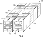
- Figure 6 is a perspective view of another embodiment of an inductor component 130 with clips serving as vertical interconnect.
- the inductor component 130 includes a dielectric body 121 (for example, a ferrite core) that includes two inductors 102a/102b (for example, copper coils) formed through the dielectric body 121.
- the inductor component 130 can be used to provide 2-phase power regulation.
- the inductor component 130 includes clips 112/114 secured to dielectric body 121. As shown in Figure 6 , surface mount components 124, such as capacitors, are connected across some of the clips 112.
- inductor component 130 By implementing the inductor component 130 in this manner, a more compact electronic assembly can be realized.
- surface mount capacitors can be placed across clips of the inductor component to achieve a more compact power module.
- the surface mount components 124 are soldered to the clips 112. In such implementations, epoxy can be added to secure the components 124 to prevent fall-off during reflow and/or high temperature solder can be used.
- surface mount components 124 can be included on any surface of the dielectric body 121.
- a recess can be formed in dielectric body and/or in a circuit board to provide clearance for the surface mount components when the electronic component is attached to the circuit board.
- Figure 7 is a perspective view of another embodiment of an inductor component 150 with clips serving as vertical interconnect.
- the inductor component 150 includes a dielectric body 141 (for example, a ferrite core) that includes two inductors 102a/102b (for example, copper coils) formed through the dielectric body 141.
- a dielectric body 141 for example, a ferrite core
- two inductors 102a/102b for example, copper coils
- the inductor component 110 includes first clips 132 secured to the dielectric body 141 and of a first size (for instance, suitable for carrying signals) and second clips 134 secured to the dielectric body 141 and of a second size (for instance, suitable for carrying power).
- Figure 8 is a perspective view of one embodiment of a power module 160 using the inductor components of Figure 7 as vertical interconnect.
- the power module 160 includes a circuit board 151, a first inductor component 150a attached to a bottom surface of the circuit board 151, and a second inductor component 150b attached to the bottom surface of the circuit board 151.
- the power module 160 of Figure 8 includes two of the inductor components of Figure 7 . Since the inductor components each include two inductors, the power module 160 includes four inductors and thus operates as a 4-phase power regulation module, in this example.
- a top side of the circuit board 151 includes surface mount components 4 and a first semiconductor die 3a, a second semiconductor die 3b, a third semiconductor 3c, and a fourth semiconductor die 3d.
- each of the semiconductor dies 3a-3d correspond to a DrMOS die including a regulator that regulates a current through a corresponding one of the inductors of inductors components 150a/150b.
- the clips 132/134 are used to carry signals and power between the circuitry on the circuit board 151 and another circuit board (for instance, a customer circuit board to which the power module 160 is soldered to when deployed for a given application).
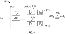
- Figure 9 is a circuit diagram of a power module 620 according to one embodiment.
- the circuit diagram depicts an example of power regulation circuitry for a single phase of power regulation.
- the power regulation circuitry can be replicated to provide regulation for multiple phases.
- the circuitry can be replicated four times to provide regulation in a 4-phase power module, such as the power module 160 of Figure 8 .
- a power module can include more phases as needed for a particular application.
- circuitry suitable for power regulation is shown, circuitry for a power module can be implemented in other ways.
- the power module 620 includes a DrMOS die 603a that regulates a current through an inductor 608a.
- the DrMOS die 603a includes a first high side power MOSFET 611a, a first low side power MOSFET 612a, a first high side driver 613a, a first low side driver 614a, and a driver logic circuit 615a.
- DrMOS dies can be implemented in other ways. Accordingly, other implementations are possible. Furthermore, although certain circuits of the DrMOS dies are depicted, DrMOS dies can include other circuitry and/or other pin configurations.
- an input control signal INa is provided to the logic 615a.
- the logic 615a controls driver signals to the high side driver 613a and the low side driver 614a, which control the high side power MOSFET 611a and low side power MOSFET 612a, respectively.
- the high side power MOSFET 611a and low side power MOSFET 612a are coupled to a first terminal VSWa of the inductor 608a to form a half bridge circuit of a switching regulator, such as a buck converter.
- the MOSFETs 612a/612b are switched on and off to control a current provided to the inductor 608a.
- a second terminal of the inductor 608a electrically connects to an output voltage pin VOUTa.
- Devices employing the above-described schemes can be implemented into various electronic devices in a wide range of applications including, but not limited to, bus converters, high current distributed power systems, telecom systems, datacom systems, storage systems, and automotive systems.
- examples of electronic devices that can be implemented with the power modules herein include, but are not limited to, communication systems, consumer electronic products, electronic test equipment, communication infrastructure, servers, automobiles, etc.
Landscapes
- Engineering & Computer Science (AREA)
- Power Engineering (AREA)
- Microelectronics & Electronic Packaging (AREA)
- Manufacturing & Machinery (AREA)
- Combinations Of Printed Boards (AREA)
Abstract
Clips serving as vertical interconnect are disclosed herein. In certain embodiments, an electronic assembly such as an electronic module includes a first circuit board and an electronic component attached to the first circuit board. The electronic component includes a dielectric body and at least one clip secured to the dielectric body. The clip is electrically connected to the first circuit board to operate as vertical interconnect.
Description
- Embodiments of the invention relate to electronic systems, and more particularly, to vertical interconnect in electronic assemblies.
- An electronic module includes passive devices, active devices, and/or semiconductor dies interconnected to perform a particular function. Such an electronic module can also include pins for providing an electrical interface to connect the electronic module to a larger electronic system.
- One example of an electronic module is a power module, which can include one or more switching regulators that operate in combination with one or more inductors to provide power regulation. For example, the switching regulator can employ switches (for instance, power transistors) coupled in series and/or parallel with an output terminal that provides an output voltage to a load through an inductor. Additionally, a controller turns the switches ON and OFF to control delivery of current pulses to the output terminal through the inductor, which converts the switched pulses into a steady load current. A power module can include a semiconductor die on which metal-oxide-semiconductor field-effect transistor (MOSFET) switches and a driver are formed. Such a semiconductor die is referred to as a driver and MOSFET (DrMOS) die or integrated circuit (IC).
- Clips serving as vertical interconnect are disclosed herein. In certain embodiments, an electronic assembly such as an electronic module includes a first circuit board and an electronic component attached to the first circuit board. The electronic component includes a dielectric body and at least one clip secured to the dielectric body. The clip is electrically connected to the first circuit board to operate as vertical interconnect. For example, the clip can be used to electrically connect the first circuit board to a second circuit board that is attached to the electronic component opposite the first circuit board. By using clips as vertical interconnect, limitations in aspect ratio for vertical interconnect is avoided. Further, since the clips are securely held by the dielectric body, the clips are not subjected to tilt and/or twist like conventional vertical interconnect. Moreover, the clips can be implemented with tight spacing.
- In one aspect, an electronic assembly includes a first circuit board and an electronic component attached to the first circuit board. The electronic component includes a dielectric body and a first clip secured to the dielectric body. The first clip is electrically connected to the first circuit board to operate as vertical interconnect.
- In another aspect, a method of providing electrical connections in an electronic assembly is provided. The method includes securing a first clip to a dielectric body of an electronic component, attaching the electronic component to a first circuit board, and using the first clip as vertical interconnect.
- In another aspect, an electronic component includes a dielectric body having a first surface, a second surface opposite the first surface, and a side. The electronic component further includes a first clip secured to the dielectric body to operate as vertical interconnect, the first clip providing an electrical connection from the first surface to the second surface along the side.
-
-
Figure 1 is a perspective view of one embodiment of an electronic component with clips serving as vertical interconnect. -
Figure 2A is a side view of one embodiment of an electronic assembly using the electronic components ofFigure 1 for providing vertical interconnects. -
Figure 2B is a side view of another embodiment of an electronic assembly using the electronic components ofFigure 1 for providing vertical interconnects. -
Figure 3 is a perspective view of one embodiment of an inductor component with clips serving as vertical interconnect. -
Figure 4 is a perspective view of another embodiment of an inductor component with clips serving as vertical interconnect. -
Figure 5 is a perspective view of another embodiment of an inductor component with clips serving as vertical interconnect. -
Figure 6 is a perspective view of another embodiment of an inductor component with clips serving as vertical interconnect. -
Figure 7 is a perspective view of another embodiment of an inductor component with clips serving as vertical interconnect. -
Figure 8 is a perspective view of one embodiment of a power module using the inductor components ofFigure 7 as vertical interconnect. -
Figure 9 is a circuit diagram of a power module according to one embodiment. - The following detailed description of embodiments presents various descriptions of specific embodiments of the invention. However, the invention can be embodied in a multitude of different ways. In this description, reference is made to the drawings where like reference numerals may indicate identical or functionally similar elements. It will be understood that elements illustrated in the figures are not necessarily drawn to scale. Moreover, it will be understood that certain embodiments can include more elements than illustrated in a drawing and/or a subset of the elements illustrated in a drawing. Further, some embodiments can incorporate any suitable combination of features from two or more drawings.
- Vertical interconnect can be used to provide vertical electrical connections in a variety of electronic assemblies. For example, an electronic assembly, such as an electronic module, can include a first circuit board and a second circuit board that are electrically connected to one another by vertical interconnect.
- Existing vertical interconnect suffers from various drawbacks. For example, certain vertical interconnects have limitations on aspect ratio, for instance, a height to width ratio of 2:1 or less. Thus, to achieve taller vertical interconnect, a footprint of the vertical interconnect increases to maintain the aspect ratio. Such an increase in footprint leads to the vertical interconnect occupying more space.
- Another limitation of existing vertical interconnect is that it can be subjected to tilt and/or twist due to stress arising during assembly. Furthermore, such vertical interconnect can be treated as a component for certain assembly processes, and thus subject to component-to-component spacing limitations and a corresponding reduction in number of vertical interconnects per unit area. Moreover, certain assembly processes specify that all vertical interconnect is the same size, thus necessitating that common-sized vertical interconnect be used for both power and signals.
- There is a need for improved vertical interconnect for electronic assemblies, including for power modules desiring to grow in a vertical direction to increase power density and/or lower thermal resistance.
- Clips serving as vertical interconnect are disclosed herein. In certain embodiments, an electronic assembly such as an electronic module includes a first circuit board and an electronic component attached to the first circuit board. The electronic component includes a dielectric body and at least one clip secured to the dielectric body. The clip is electrically connected to the first circuit board to operate as vertical interconnect.
- For example, the clip can be used to electrically connect the first circuit board to a second circuit board that is attached to the electronic component opposite the first circuit board.
- By using clips as vertical interconnect, limitations in aspect ratio for vertical interconnect is avoided. Further, since the clips are securely held by the dielectric body, the clips are not subjected to tilt and/or twist like conventional vertical interconnect. Moreover, the clips can be implemented with tight spacing.
- In certain implementations, two or more clips are secured to the dielectric body and used as vertical interconnect. When including multiple clips, the clips can have the same or different sizes, depending on application.
- For example, when used to carry both power and signals, the clips can have different sizes for power connections relative to signal connections. For instance, a power supply voltage connection may be associated with higher transient current relative to a signal connection, and thus may be implemented with a larger size and lower resistivity. Accordingly, the clips can have varying sizes for power and signals, with each clip having a size tailored for the specific electrical connection that the clip is providing.
- In certain implementations, each clip includes a top portion on a top surface of the dielectric body, a bottom portion on a bottom surface of the dielectric body, and a side portion connecting the top portion to the bottom portion along a side of the dielectric body.
- Thus, the clips wrap around a side of the dielectric body to provide an electrical connection from the above the dielectric body to below the dielectric body. The clips can be made of metal, for instance, copper. The clips are also referred to herein as staples.
- The clips can be attached to a wide variety of electronic components to facilitate providing vertical electrical connections in electronic assemblies, such as electronic modules.
- In certain implementations, the electronic component corresponds to an inductor component. For example, the inductor component can include a dielectric body (for example, a ferrite core) through which one or more inductors (for instance, copper windings) are formed, and the clips can be secured to the dielectric body to provide vertical interconnect. In such implementations, a more compact and efficient power module is realized by providing vertical interconnect along the sides of the inductor component to allow more volume in the body for the inductors.
- The clips can be attached to the dielectric body of the electronic component in any suitable way. In a first example, a clip is secured to a dielectric body using an adhesive. In a second example, a clip is plated on the dielectric body using any suitable plating process. In a third example, the clip is soldered to the dielectric body. In a fourth example, a recess is formed in the dielectric body, and the clip rests in the recess. Placing clips in recesses of the dielectric body can be particularly useful for implementations in which the clips having varying thicknesses and it is desirable for the clips to be co-planar with one another to provide a flat electrical interface to a circuit board. Thus, for example, a thicker clip for carrying power can be placed in a recess so that it is flush with thinner clips used for carrying signals.
- In certain implementations, at least one semiconductor die is attached to the first circuit board. When implemented as a power module, the at least one semiconductor die (for instance, one or more DrMOS die) can operate in combination with an inductor of the inductor component to form a power module. For instance, the number of inductors included in the inductor component can correspond to a desired number of phases for power regulation, and thus a single-phase power module, a two-phase (2-phase) power module, four-phase (4-phase) power module, or other desired power module can be realized.
- Surface mount components, such as capacitors, can also be attached in various locations in the electronic assembly. Such surface mount components can be included not only on a circuit board, but also on the electronic component that includes the clips. For example, surface mount components can be included on top, bottom, and/or side surfaces of the electronic component. Such surface mount components can be electrically connected to one or more of the clips to aid in achieving desired circuit operation.
-
Figure 1 is a perspective view of one embodiment of anelectronic component 10. Theelectronic component 10 includes a dielectric body 1 and clips 2. Each of theclips 2 is secured to the dielectric body to serve as vertical interconnect. - In the illustrated embodiment, the dielectric body 1 is shaped substantially as a rectangular prism. Additionally, each of the
clips 2 wraps from a top surface to a bottom surface of the dielectric body 1 around a side of the dielectric body 1. Although an example of a dielectric body shaped as a rectangular prism is shown, the teachings herein are applicable to dielectric bodies of other shapes. - The
clips 2 are electrically conductive, while the dielectric body 1 is nonconductive and formed of any suitable dielectric. In certain implementations, theclips 2 are formed of metal, for instance, copper. - In the illustrated embodiment, three of the
clips 2 are secured to a left side of the dielectric body 1, while another three of theclips 2 are secured to a right side of the dielectric body 1. Although an example with six clips is shown, theelectronic component 10 can include more or fewer clips. Further, theclips 2 can be arranged on the dielectric body 1 in other ways, for instance, on more or fewer sides of the dielectric body or in a different arrangement along the sides. Accordingly, other implementations are possible. - The
clips 2 can be attached to the dielectric body 1 in any suitable way, for instance, using an adhesive. In some implementations, theclips 2 are plated to the dielectric body 1 using a plating process and/or placed in recesses in the dielectric body 1. -
Figure 2A is a side view of one embodiment of anelectronic assembly 20 using the electronic components ofFigure 1 for providing vertical interconnects. Theelectronic assembly 10 includes afirst circuit board 11, asecond circuit board 12, a firstelectronic component 10a, and a secondelectronic component 10b. - In the illustrated embodiment, clips 2a are secured to the first
electronic component 10a, whileclips 2b are secured to the secondelectronic component 10b. Theclips 2a/2b are used to provide electrical connections from thefirst circuit board 11 to thesecond circuit board 12. For example, theclips 2a/2b can be used to carry power (for example, a supply voltage and/or ground) and/or signals between thecircuit boards 11/12 as desired. - By using clips as vertical interconnect, limitations in aspect ratio for vertical interconnect is avoided. Further, since the clips are securely held by the dielectric body, the clips are not subjected to tilt and/or twist like conventional vertical interconnect. Moreover, the clips can be implemented with tight spacing.
- In certain implementations, each clip includes a top portion on a top surface of the dielectric body, a bottom portion on a bottom surface of the dielectric body, and a side portion connecting the top portion to the bottom portion along a side of the dielectric body. For example, the
clip 2a includes a top portion 2a1, a bottom portion 2a2 and a side portion 2a3. Thus, the clips can wrap around a side of the dielectric body to provide an electrical connection from above the dielectric body to below the dielectric body. - As shown in
Figure 2A , the top portion 2a1 is interposed between thedielectric body 1a and thefirst circuit board 11, while the bottom portion 2a2 is interposed between thedielectric body 1a and thesecond circuit board 12. The top portion 2a1 is electrically connected (for instance, soldered) to a corresponding electrical terminal of thefirst circuit board 11, while the bottom portion 2a2 is electrically connected (for instance, soldered) to a corresponding electrical terminal of thesecond circuit board 12. -
Figure 2B is a side view of another embodiment of anelectronic assembly 30 using the electronic components ofFigure 1 for providing vertical interconnects. - The
electronic module 30 ofFigure 2B is similar to theelectronic assembly 20 of Figure 1B, except that the electronic assembly depicts various semiconductor dies 3, surface mount components 4, andelectrical connectors 5 included on thecircuit boards 11/12 as shown. The electronic circuitry on thefirst circuit board 11 can be electrically connected to the electronic circuitry of thesecond circuit board 12 using theclips 2a/2b. Thus, the semiconductor dies 3, surface mount components 4, andelectrical connectors 5 can be interconnected as desired to achieve a particular function. - Although one example of electronic circuitry for each circuit board is shown, the circuit boards can include electronic circuitry implemented in a wide variety of ways. Accordingly, other implementations are possible.
- Any of the electronic components herein can be included in an electronic assembly to provide vertical interconnects. In some implementations, the electronic assembly is an electronic module, such as a power module.
-
Figure 3 is a perspective view of one embodiment of aninductor component 100 with clips serving as vertical interconnect. Theinductor component 100 includes a dielectric body 91 (for example, a ferrite core) through which an inductor 92 (for example, a copper winding) has been formed. Thedielectric body 91 also includes agroove 93 through thedielectric body 91 to aid in achieving desired inductance characteristics for theinductor component 100. - As shown in
Figure 3 , clips 2 have been secured to a side of thedielectric body 91 of theinductor component 100. - Securing
clips 2 to an inductor component to provide vertical interconnect can provide several advantages. For example, providing vertical interconnect along the sides of theinductor component 100 allow more volume for inductors. Furthermore, when used to provide vertical interconnect in a power module, theclips 2 increase the compactness and/or efficiency of the power module. -
Figure 4 is a perspective view of another embodiment of aninductor component 110 with clips serving as vertical interconnect. - In the illustrated embodiment, the
inductor component 110 includes a dielectric body 101 (for example, a ferrite core) that includes fourinductors 102a/102b/102c/102d (for example, copper coils) formed through thedielectric body 101. Thus, fourinductors 102a/102b/102c/102d are provided, which makes theinductor component 110 well-suited for a 4-phase power regulation application. - The
inductor component 110 includesfirst clips 112 secured to thedielectric body 101 and of a first size (for instance, suitable for carrying signals) andsecond clips 114 secured to thedielectric body 101 and of a second size (for instance, suitable for carrying power). - In certain implementations, clips of different sizes are secured to a dielectric body of an electronic component.
- For example, when used to carry both power and signals, the clips can have different sizes for power connections relative to signal connections. For instance, a power supply voltage connection may be associated with higher transient current relative to a signal connection, and thus may be implemented with a larger size and lower resistivity. Accordingly, the clips can have varying sizes for power and signals, with each clip having a size tailored for the specific electrical connection that the clip is providing.
-
Figure 5 is a perspective view of another embodiment of aninductor component 120 with clips serving as vertical interconnect. - The
inductor component 120 ofFigure 5 is similar to theinductor component 110 ofFigure 4 , except that theinductor component 120 ofFigure 5 includesfirst clips 122 that are plated to thedielectric body 101. Thefirst clips 122 can be used for carrying signals and/or providing other desired electrical connections. - Thus, a combination of
first clips 122 that are plated andsecond clips 114 that are not plated are secured to thedielectric body 101, in this embodiment. In certain implementations, thesecond clips 114 are wider and thicker (for example, to carry power) than thefirst clips 122 and are secured to thedielectric body 101 using an adhesive. -
Figure 6 is a perspective view of another embodiment of aninductor component 130 with clips serving as vertical interconnect. - In the illustrated embodiment, the
inductor component 130 includes a dielectric body 121 (for example, a ferrite core) that includes twoinductors 102a/102b (for example, copper coils) formed through thedielectric body 121. Theinductor component 130 can be used to provide 2-phase power regulation. - The
inductor component 130 includesclips 112/114 secured todielectric body 121. As shown inFigure 6 ,surface mount components 124, such as capacitors, are connected across some of theclips 112. - By implementing the
inductor component 130 in this manner, a more compact electronic assembly can be realized. For example, in a power regulation application, surface mount capacitors can be placed across clips of the inductor component to achieve a more compact power module. In some implementations, thesurface mount components 124 are soldered to theclips 112. In such implementations, epoxy can be added to secure thecomponents 124 to prevent fall-off during reflow and/or high temperature solder can be used. - Although shown as being attached to a side surface of the
inductor component 130,surface mount components 124 can be included on any surface of thedielectric body 121. - When included on the top or bottom surface of a dielectric body, a recess can be formed in dielectric body and/or in a circuit board to provide clearance for the surface mount components when the electronic component is attached to the circuit board.
-
Figure 7 is a perspective view of another embodiment of aninductor component 150 with clips serving as vertical interconnect. - The
inductor component 150 includes a dielectric body 141 (for example, a ferrite core) that includes twoinductors 102a/102b (for example, copper coils) formed through thedielectric body 141. - The
inductor component 110 includesfirst clips 132 secured to thedielectric body 141 and of a first size (for instance, suitable for carrying signals) andsecond clips 134 secured to thedielectric body 141 and of a second size (for instance, suitable for carrying power). -
Figure 8 is a perspective view of one embodiment of apower module 160 using the inductor components ofFigure 7 as vertical interconnect. For example, thepower module 160 includes acircuit board 151, afirst inductor component 150a attached to a bottom surface of thecircuit board 151, and asecond inductor component 150b attached to the bottom surface of thecircuit board 151. - The
power module 160 ofFigure 8 includes two of the inductor components ofFigure 7 . Since the inductor components each include two inductors, thepower module 160 includes four inductors and thus operates as a 4-phase power regulation module, in this example. - In the illustrated embodiment, a top side of the
circuit board 151 includes surface mount components 4 and afirst semiconductor die 3a, a second semiconductor die 3b, a third semiconductor 3c, and afourth semiconductor die 3d. In certain implementations, each of the semiconductor dies 3a-3d correspond to a DrMOS die including a regulator that regulates a current through a corresponding one of the inductors ofinductors components 150a/150b. - The
clips 132/134 are used to carry signals and power between the circuitry on thecircuit board 151 and another circuit board (for instance, a customer circuit board to which thepower module 160 is soldered to when deployed for a given application). -
Figure 9 is a circuit diagram of apower module 620 according to one embodiment. - The circuit diagram depicts an example of power regulation circuitry for a single phase of power regulation. However, the power regulation circuitry can be replicated to provide regulation for multiple phases. For example, the circuitry can be replicated four times to provide regulation in a 4-phase power module, such as the
power module 160 ofFigure 8 . - Accordingly, although an example of a single-phase power module is depicted, a power module can include more phases as needed for a particular application. Furthermore, although one example of circuitry suitable for power regulation is shown, circuitry for a power module can be implemented in other ways.
- In the illustrated embodiment, the
power module 620 includes aDrMOS die 603a that regulates a current through aninductor 608a. The DrMOS die 603a includes a first highside power MOSFET 611a, a first lowside power MOSFET 612a, a firsthigh side driver 613a, a firstlow side driver 614a, and adriver logic circuit 615a. - Although one example of a DrMOS die is shown, DrMOS dies can be implemented in other ways. Accordingly, other implementations are possible. Furthermore, although certain circuits of the DrMOS dies are depicted, DrMOS dies can include other circuitry and/or other pin configurations.
- In the illustrated embodiment, an input control signal INa is provided to the
logic 615a. Thelogic 615a controls driver signals to thehigh side driver 613a and thelow side driver 614a, which control the highside power MOSFET 611a and lowside power MOSFET 612a, respectively. The highside power MOSFET 611a and lowside power MOSFET 612a are coupled to a first terminal VSWa of theinductor 608a to form a half bridge circuit of a switching regulator, such as a buck converter. TheMOSFETs 612a/612b are switched on and off to control a current provided to theinductor 608a. A second terminal of theinductor 608a electrically connects to an output voltage pin VOUTa. - Devices employing the above-described schemes can be implemented into various electronic devices in a wide range of applications including, but not limited to, bus converters, high current distributed power systems, telecom systems, datacom systems, storage systems, and automotive systems. Thus, examples of electronic devices that can be implemented with the power modules herein include, but are not limited to, communication systems, consumer electronic products, electronic test equipment, communication infrastructure, servers, automobiles, etc.
- The foregoing description may refer to elements or features as being "connected" or "coupled" together. As used herein, unless expressly stated otherwise, "connected" means that one element/feature is directly or indirectly connected to another element/feature, and not necessarily mechanically. Likewise, unless expressly stated otherwise, "coupled" means that one element/feature is directly or indirectly coupled to another element/feature, and not necessarily mechanically. Thus, although the various schematics shown in the figures depict example arrangements of elements and components, additional intervening elements, devices, features, or components may be present in an actual embodiment (assuming that the functionality of the depicted circuits is not adversely affected).
- While certain embodiments have been described, these embodiments have been presented by way of example only and are not intended to limit the scope of the disclosure. Indeed, the novel apparatus, methods, and systems described herein may be embodied in a variety of other forms; furthermore, various omissions, substitutions, and changes in the form of the methods and systems described herein may be made without departing from the spirit of the disclosure. For example, while the disclosed embodiments are presented in a given arrangement, alternative embodiments may perform similar functionalities with different components and/or circuit topologies, and some elements may be deleted, moved, added, subdivided, combined, and/or modified. Each of these elements may be implemented in a variety of different ways. Any suitable combination of the elements and acts of the various embodiments described above can be combined to provide further embodiments. Accordingly, the scope of the present invention is defined only by reference to the appended claims.
- Although the claims presented here are in single dependency format for filing at the USPTO, it is to be understood that any claim may depend on any preceding claim of the same type except when that is clearly not technically feasible.
- By way of non-limiting example, some aspects of the disclosure are set out in the following numbered clauses.
- Numbered Clause 1. An electronic assembly comprising:
- a first circuit board; and
- an electronic component attached to the first circuit board, the electronic component including a dielectric body and a first clip secured to the dielectric body,
- wherein the first clip is electrically connected to the first circuit board to operate as vertical interconnect.
- Numbered
Clause 2. The electronic assembly of Numbered Clause 1, further comprising a second circuit board attached to the electronic component opposite the first circuit board, wherein first clip electrically connects the first circuit board to the second circuit board. - Numbered
Clause 3. The electronic assembly ofNumbered Clause 1 or 2, wherein the electronic component is an inductor component. - Numbered Clause 4. The electronic assembly of
Numbered Clause 3, wherein the dielectric body is a ferrite core, the inductor component including one or more inductors formed through the ferrite core. - Numbered
Clause 5. The electronic assembly of any preceding Numbered Clause, wherein the first clip comprises a metal. - Numbered Clause 6. The electronic assembly of
Numbered Clause 5, wherein the metal is copper. - Numbered Clause 7. The electronic assembly of any preceding Numbered Clause, further comprising a second clip secured to the electronic component and electrically connected to the first circuit board to operate as vertical interconnect.
- Numbered Clause 8. The electronic assembly of Numbered Clause 7, wherein the first clip carries a signal and the second clip carries power.
- Numbered Clause 9. The electronic assembly of any preceding Numbered Clause, wherein the first clip and the second clip have different sizes.
- Numbered
Clause 10. The electronic assembly of any preceding Numbered Clause, further comprising a component mounted across the first clip and the second clip. - Numbered
Clause 11. The electronic assembly of any preceding Numbered Clause, wherein the first clip is plated on the dielectric body. - Numbered
Clause 12. The electronic assembly of any preceding Numbered Clause, wherein the first clip is attached to the dielectric body by an adhesive. - Numbered Clause 13. A method of providing electrical connections in an electronic assembly, the method comprising:
- securing a first clip to a dielectric body of an electronic component;
- attaching the electronic component to a first circuit board; and
- using the first clip as vertical interconnect.
- Numbered Clause 14. The method of Numbered Clause 13, further comprising attaching a second circuit board to the electronic component opposite the first circuit board and using the first clip as vertical interconnect between the first circuit board to the second circuit board.
- Numbered Clause 15. The method of Numbered Clause 13 or 14, wherein the electronic component is an inductor component including at least one inductor formed through the dielectric body.
- Numbered Clause 16. The method of any of Numbered Clauses 13 to 15, wherein the first clip comprises a metal.
- Numbered Clause 17. The method of any of Numbered Clauses 13 to 16, further securing a second clip to the electronic component, and using the second clip as vertical interconnect.
- Numbered Clause 18. The method of Numbered Clause 17, further comprising carrying a signal using the first clip and carrying power using the second clip.
- Numbered Clause 19. An electronic component comprising:
- a dielectric body having a first surface, a second surface opposite the first surface, and a side; and
- a first clip secured to the dielectric body to operate as vertical interconnect, the first clip providing an electrical connection from the first surface to the second surface along the side.
- Numbered
Clause 20. The electronic component of Numbered Clause 19, further comprising an inductor formed through the dielectric body.
Claims (15)
- An electronic assembly comprising:a first circuit board; andan electronic component attached to the first circuit board, the electronic component including a dielectric body and a first clip secured to the dielectric body,wherein the first clip is electrically connected to the first circuit board to operate as vertical interconnect.
- The electronic assembly of claim 1, further comprising a second circuit board attached to the electronic component opposite the first circuit board, wherein first clip electrically connects the first circuit board to the second circuit board.
- The electronic assembly of claim 1 or 2, wherein the electronic component is an inductor component, preferably wherein the dielectric body is a ferrite core, the inductor component including one or more inductors formed through the ferrite core.
- The electronic assembly of any preceding claim, wherein the first clip comprises a metal, preferably wherein the metal is copper.
- The electronic assembly of any preceding claim, further comprising a second clip secured to the electronic component and electrically connected to the first circuit board to operate as vertical interconnect, preferably wherein the first clip carries a signal and the second clip carries power.
- The electronic assembly of any preceding claim, wherein the first clip and the second clip have different sizes.
- The electronic assembly of any preceding claim, further comprising a component mounted across the first clip and the second clip.
- The electronic assembly of any preceding claim, wherein the first clip is plated on the dielectric body and/or wherein the first clip is attached to the dielectric body by an adhesive.
- A method of providing electrical connections in an electronic assembly, the method comprising:securing a first clip to a dielectric body of an electronic component;attaching the electronic component to a first circuit board; andusing the first clip as vertical interconnect.
- The method of claim 9, further comprising attaching a second circuit board to the electronic component opposite the first circuit board and using the first clip as vertical interconnect between the first circuit board to the second circuit board.
- The method of claim 9 or 10, wherein the electronic component is an inductor component including at least one inductor formed through the dielectric body.
- The method of any of claims 9 to 11, wherein the first clip comprises a metal.
- The method of any of claims 9 to 12, further securing a second clip to the electronic component, and using the second clip as vertical interconnect, preferably further comprising carrying a signal using the first clip and carrying power using the second clip.
- An electronic component comprising:a dielectric body having a first surface, a second surface opposite the first surface, and a side; anda first clip secured to the dielectric body to operate as vertical interconnect, the first clip providing an electrical connection from the first surface to the second surface along the side.
- The electronic component of claim 14, further comprising an inductor formed through the dielectric body.
Applications Claiming Priority (2)
| Application Number | Priority Date | Filing Date | Title |
|---|---|---|---|
| US202363600230P | 2023-11-17 | 2023-11-17 | |
| US18/935,232 US20250168966A1 (en) | 2023-11-17 | 2024-11-01 | Clips serving as vertical interconnect |
Publications (1)
| Publication Number | Publication Date |
|---|---|
| EP4557895A1 true EP4557895A1 (en) | 2025-05-21 |
Family
ID=93521578
Family Applications (1)
| Application Number | Title | Priority Date | Filing Date |
|---|---|---|---|
| EP24212728.0A Pending EP4557895A1 (en) | 2023-11-17 | 2024-11-13 | Clips serving as vertical interconnect |
Country Status (3)
| Country | Link |
|---|---|
| US (1) | US20250168966A1 (en) |
| EP (1) | EP4557895A1 (en) |
| CN (1) | CN120021107A (en) |
Citations (2)
| Publication number | Priority date | Publication date | Assignee | Title |
|---|---|---|---|---|
| US20090175014A1 (en) * | 2008-01-03 | 2009-07-09 | Jian-Hong Zeng | Assembled circuit and electronic component |
| WO2019051346A1 (en) * | 2017-09-08 | 2019-03-14 | Kemet Electronics Corporation | High density multi-component and serial packages |
-
2024
- 2024-11-01 US US18/935,232 patent/US20250168966A1/en active Pending
- 2024-11-13 EP EP24212728.0A patent/EP4557895A1/en active Pending
- 2024-11-15 CN CN202411630398.7A patent/CN120021107A/en active Pending
Patent Citations (2)
| Publication number | Priority date | Publication date | Assignee | Title |
|---|---|---|---|---|
| US20090175014A1 (en) * | 2008-01-03 | 2009-07-09 | Jian-Hong Zeng | Assembled circuit and electronic component |
| WO2019051346A1 (en) * | 2017-09-08 | 2019-03-14 | Kemet Electronics Corporation | High density multi-component and serial packages |
Also Published As
| Publication number | Publication date |
|---|---|
| CN120021107A (en) | 2025-05-20 |
| US20250168966A1 (en) | 2025-05-22 |
Similar Documents
| Publication | Publication Date | Title |
|---|---|---|
| US11503710B2 (en) | Power module | |
| US9697947B1 (en) | Vertical PCB surface mount inductors and power converters | |
| US8952776B2 (en) | Powder core material coupled inductors and associated methods | |
| CN112038054B (en) | Voltage regulation module | |
| US11456106B2 (en) | Inductor component and power supply module | |
| US20250318052A1 (en) | Sandwich structure power supply module | |
| US12471218B2 (en) | Sandwich structure power supply module | |
| US20230396158A1 (en) | Sandwich structure power supply module | |
| US20250247959A1 (en) | Sandwich structure power supply module | |
| US11683889B2 (en) | Processor interposer and electronic system including the processor interposer | |
| JP4008195B2 (en) | Power converter and manufacturing method thereof | |
| WO2008134350A2 (en) | Inductive element for a multi-phase interleaved power supply and apparatus and methods using the same | |
| US20250168966A1 (en) | Clips serving as vertical interconnect | |
| US20250337324A1 (en) | Trans-inductor voltage regulator (tlvr) inductor module and power electronics assembly including the tlvr inductor module | |
| US20250095902A1 (en) | Inductor assembly and power module using the same | |
| CN119483185A (en) | A sandwich structure power module | |
| US20220336138A1 (en) | Magnetic device and power conversion module | |
| CN119210088A (en) | Integrated component and integrated power converter module | |
| US20260113848A1 (en) | Compact power modules | |
| US20260032933A1 (en) | Compact inductors | |
| TW201915636A (en) | Power converter module | |
| US20260058547A1 (en) | Vertically stacked power module and associated inductor assembly | |
| US20250273389A1 (en) | Coupled inductor and voltage regulator | |
| US20230260690A1 (en) | Inductor Mountable on a Circuit Board | |
| US20260005133A1 (en) | Integrated mmc package with inductor and die |
Legal Events
| Date | Code | Title | Description |
|---|---|---|---|
| PUAI | Public reference made under article 153(3) epc to a published international application that has entered the european phase |
Free format text: ORIGINAL CODE: 0009012 |
|
| STAA | Information on the status of an ep patent application or granted ep patent |
Free format text: STATUS: REQUEST FOR EXAMINATION WAS MADE |
|
| 17P | Request for examination filed |
Effective date: 20241113 |
|
| AK | Designated contracting states |
Kind code of ref document: A1 Designated state(s): AL AT BE BG CH CY CZ DE DK EE ES FI FR GB GR HR HU IE IS IT LI LT LU LV MC ME MK MT NL NO PL PT RO RS SE SI SK SM TR |