EP4557536A1 - Receptacle connector, electronic device, and assembly method - Google Patents
Receptacle connector, electronic device, and assembly method Download PDFInfo
- Publication number
- EP4557536A1 EP4557536A1 EP23859319.8A EP23859319A EP4557536A1 EP 4557536 A1 EP4557536 A1 EP 4557536A1 EP 23859319 A EP23859319 A EP 23859319A EP 4557536 A1 EP4557536 A1 EP 4557536A1
- Authority
- EP
- European Patent Office
- Prior art keywords
- receptacle connector
- connecting part
- electronic device
- circuit board
- terminal board
- Prior art date
- Legal status (The legal status is an assumption and is not a legal conclusion. Google has not performed a legal analysis and makes no representation as to the accuracy of the status listed.)
- Pending
Links
Images




Classifications
-
- H—ELECTRICITY
- H01—ELECTRIC ELEMENTS
- H01R—ELECTRICALLY-CONDUCTIVE CONNECTIONS; STRUCTURAL ASSOCIATIONS OF A PLURALITY OF MUTUALLY-INSULATED ELECTRICAL CONNECTING ELEMENTS; COUPLING DEVICES; CURRENT COLLECTORS
- H01R12/00—Structural associations of a plurality of mutually-insulated electrical connecting elements, specially adapted for printed circuits, e.g. printed circuit boards [PCB], flat or ribbon cables, or like generally planar structures, e.g. terminal strips, terminal blocks; Coupling devices specially adapted for printed circuits, flat or ribbon cables, or like generally planar structures; Terminals specially adapted for contact with, or insertion into, printed circuits, flat or ribbon cables, or like generally planar structures
- H01R12/70—Coupling devices
- H01R12/71—Coupling devices for rigid printing circuits or like structures
- H01R12/712—Coupling devices for rigid printing circuits or like structures co-operating with the surface of the printed circuit or with a coupling device exclusively provided on the surface of the printed circuit
- H01R12/716—Coupling device provided on the PCB
-
- H—ELECTRICITY
- H01—ELECTRIC ELEMENTS
- H01R—ELECTRICALLY-CONDUCTIVE CONNECTIONS; STRUCTURAL ASSOCIATIONS OF A PLURALITY OF MUTUALLY-INSULATED ELECTRICAL CONNECTING ELEMENTS; COUPLING DEVICES; CURRENT COLLECTORS
- H01R12/00—Structural associations of a plurality of mutually-insulated electrical connecting elements, specially adapted for printed circuits, e.g. printed circuit boards [PCB], flat or ribbon cables, or like generally planar structures, e.g. terminal strips, terminal blocks; Coupling devices specially adapted for printed circuits, flat or ribbon cables, or like generally planar structures; Terminals specially adapted for contact with, or insertion into, printed circuits, flat or ribbon cables, or like generally planar structures
- H01R12/70—Coupling devices
- H01R12/7005—Guiding, mounting, polarizing or locking means; Extractors
- H01R12/7011—Locking or fixing a connector to a PCB
- H01R12/707—Soldering or welding
-
- H—ELECTRICITY
- H01—ELECTRIC ELEMENTS
- H01R—ELECTRICALLY-CONDUCTIVE CONNECTIONS; STRUCTURAL ASSOCIATIONS OF A PLURALITY OF MUTUALLY-INSULATED ELECTRICAL CONNECTING ELEMENTS; COUPLING DEVICES; CURRENT COLLECTORS
- H01R13/00—Details of coupling devices of the kinds covered by groups H01R12/70 or H01R24/00 - H01R33/00
- H01R13/02—Contact members
-
- H—ELECTRICITY
- H01—ELECTRIC ELEMENTS
- H01R—ELECTRICALLY-CONDUCTIVE CONNECTIONS; STRUCTURAL ASSOCIATIONS OF A PLURALITY OF MUTUALLY-INSULATED ELECTRICAL CONNECTING ELEMENTS; COUPLING DEVICES; CURRENT COLLECTORS
- H01R13/00—Details of coupling devices of the kinds covered by groups H01R12/70 or H01R24/00 - H01R33/00
- H01R13/40—Securing contact members in or to a base or case; Insulating of contact members
-
- H—ELECTRICITY
- H01—ELECTRIC ELEMENTS
- H01R—ELECTRICALLY-CONDUCTIVE CONNECTIONS; STRUCTURAL ASSOCIATIONS OF A PLURALITY OF MUTUALLY-INSULATED ELECTRICAL CONNECTING ELEMENTS; COUPLING DEVICES; CURRENT COLLECTORS
- H01R13/00—Details of coupling devices of the kinds covered by groups H01R12/70 or H01R24/00 - H01R33/00
- H01R13/46—Bases; Cases
- H01R13/502—Bases; Cases composed of different pieces
-
- H—ELECTRICITY
- H01—ELECTRIC ELEMENTS
- H01R—ELECTRICALLY-CONDUCTIVE CONNECTIONS; STRUCTURAL ASSOCIATIONS OF A PLURALITY OF MUTUALLY-INSULATED ELECTRICAL CONNECTING ELEMENTS; COUPLING DEVICES; CURRENT COLLECTORS
- H01R13/00—Details of coupling devices of the kinds covered by groups H01R12/70 or H01R24/00 - H01R33/00
- H01R13/73—Means for mounting coupling parts to apparatus or structures, e.g. to a wall
-
- H—ELECTRICITY
- H01—ELECTRIC ELEMENTS
- H01R—ELECTRICALLY-CONDUCTIVE CONNECTIONS; STRUCTURAL ASSOCIATIONS OF A PLURALITY OF MUTUALLY-INSULATED ELECTRICAL CONNECTING ELEMENTS; COUPLING DEVICES; CURRENT COLLECTORS
- H01R4/00—Electrically-conductive connections between two or more conductive members in direct contact, i.e. touching one another; Means for effecting or maintaining such contact; Electrically-conductive connections having two or more spaced connecting locations for conductors and using contact members penetrating insulation
- H01R4/02—Soldered or welded connections
- H01R4/027—Soldered or welded connections comprising means for positioning or holding the parts to be soldered or welded
-
- H—ELECTRICITY
- H01—ELECTRIC ELEMENTS
- H01R—ELECTRICALLY-CONDUCTIVE CONNECTIONS; STRUCTURAL ASSOCIATIONS OF A PLURALITY OF MUTUALLY-INSULATED ELECTRICAL CONNECTING ELEMENTS; COUPLING DEVICES; CURRENT COLLECTORS
- H01R43/00—Apparatus or processes specially adapted for manufacturing, assembling, maintaining, or repairing of line connectors or current collectors or for joining electric conductors
-
- H—ELECTRICITY
- H01—ELECTRIC ELEMENTS
- H01R—ELECTRICALLY-CONDUCTIVE CONNECTIONS; STRUCTURAL ASSOCIATIONS OF A PLURALITY OF MUTUALLY-INSULATED ELECTRICAL CONNECTING ELEMENTS; COUPLING DEVICES; CURRENT COLLECTORS
- H01R43/00—Apparatus or processes specially adapted for manufacturing, assembling, maintaining, or repairing of line connectors or current collectors or for joining electric conductors
- H01R43/02—Apparatus or processes specially adapted for manufacturing, assembling, maintaining, or repairing of line connectors or current collectors or for joining electric conductors for soldered or welded connections
- H01R43/0256—Apparatus or processes specially adapted for manufacturing, assembling, maintaining, or repairing of line connectors or current collectors or for joining electric conductors for soldered or welded connections for soldering or welding connectors to a printed circuit board
-
- H—ELECTRICITY
- H01—ELECTRIC ELEMENTS
- H01R—ELECTRICALLY-CONDUCTIVE CONNECTIONS; STRUCTURAL ASSOCIATIONS OF A PLURALITY OF MUTUALLY-INSULATED ELECTRICAL CONNECTING ELEMENTS; COUPLING DEVICES; CURRENT COLLECTORS
- H01R43/00—Apparatus or processes specially adapted for manufacturing, assembling, maintaining, or repairing of line connectors or current collectors or for joining electric conductors
- H01R43/02—Apparatus or processes specially adapted for manufacturing, assembling, maintaining, or repairing of line connectors or current collectors or for joining electric conductors for soldered or welded connections
- H01R43/0263—Apparatus or processes specially adapted for manufacturing, assembling, maintaining, or repairing of line connectors or current collectors or for joining electric conductors for soldered or welded connections for positioning or holding parts during soldering or welding process
-
- H—ELECTRICITY
- H01—ELECTRIC ELEMENTS
- H01R—ELECTRICALLY-CONDUCTIVE CONNECTIONS; STRUCTURAL ASSOCIATIONS OF A PLURALITY OF MUTUALLY-INSULATED ELECTRICAL CONNECTING ELEMENTS; COUPLING DEVICES; CURRENT COLLECTORS
- H01R43/00—Apparatus or processes specially adapted for manufacturing, assembling, maintaining, or repairing of line connectors or current collectors or for joining electric conductors
- H01R43/20—Apparatus or processes specially adapted for manufacturing, assembling, maintaining, or repairing of line connectors or current collectors or for joining electric conductors for assembling or disassembling contact members with insulating base, case or sleeve
-
- H—ELECTRICITY
- H01—ELECTRIC ELEMENTS
- H01R—ELECTRICALLY-CONDUCTIVE CONNECTIONS; STRUCTURAL ASSOCIATIONS OF A PLURALITY OF MUTUALLY-INSULATED ELECTRICAL CONNECTING ELEMENTS; COUPLING DEVICES; CURRENT COLLECTORS
- H01R12/00—Structural associations of a plurality of mutually-insulated electrical connecting elements, specially adapted for printed circuits, e.g. printed circuit boards [PCB], flat or ribbon cables, or like generally planar structures, e.g. terminal strips, terminal blocks; Coupling devices specially adapted for printed circuits, flat or ribbon cables, or like generally planar structures; Terminals specially adapted for contact with, or insertion into, printed circuits, flat or ribbon cables, or like generally planar structures
- H01R12/70—Coupling devices
- H01R12/71—Coupling devices for rigid printing circuits or like structures
- H01R12/72—Coupling devices for rigid printing circuits or like structures coupling with the edge of the rigid printed circuits or like structures
- H01R12/722—Coupling devices for rigid printing circuits or like structures coupling with the edge of the rigid printed circuits or like structures coupling devices mounted on the edge of the printed circuits
-
- H—ELECTRICITY
- H01—ELECTRIC ELEMENTS
- H01R—ELECTRICALLY-CONDUCTIVE CONNECTIONS; STRUCTURAL ASSOCIATIONS OF A PLURALITY OF MUTUALLY-INSULATED ELECTRICAL CONNECTING ELEMENTS; COUPLING DEVICES; CURRENT COLLECTORS
- H01R13/00—Details of coupling devices of the kinds covered by groups H01R12/70 or H01R24/00 - H01R33/00
- H01R13/46—Bases; Cases
- H01R13/52—Dustproof, splashproof, drip-proof, waterproof, or flameproof cases
- H01R13/5202—Sealing means between parts of housing or between housing part and a wall, e.g. sealing rings
-
- H—ELECTRICITY
- H01—ELECTRIC ELEMENTS
- H01R—ELECTRICALLY-CONDUCTIVE CONNECTIONS; STRUCTURAL ASSOCIATIONS OF A PLURALITY OF MUTUALLY-INSULATED ELECTRICAL CONNECTING ELEMENTS; COUPLING DEVICES; CURRENT COLLECTORS
- H01R13/00—Details of coupling devices of the kinds covered by groups H01R12/70 or H01R24/00 - H01R33/00
- H01R13/648—Protective earth or shield arrangements on coupling devices, e.g. anti-static shielding
- H01R13/658—High frequency shielding arrangements, e.g. against EMI [Electro-Magnetic Interference] or EMP [Electro-Magnetic Pulse]
- H01R13/6591—Specific features or arrangements of connection of shield to conductive members
- H01R13/6594—Specific features or arrangements of connection of shield to conductive members the shield being mounted on a PCB and connected to conductive members
-
- H—ELECTRICITY
- H01—ELECTRIC ELEMENTS
- H01R—ELECTRICALLY-CONDUCTIVE CONNECTIONS; STRUCTURAL ASSOCIATIONS OF A PLURALITY OF MUTUALLY-INSULATED ELECTRICAL CONNECTING ELEMENTS; COUPLING DEVICES; CURRENT COLLECTORS
- H01R2201/00—Connectors or connections adapted for particular applications
- H01R2201/06—Connectors or connections adapted for particular applications for computer periphery
-
- H—ELECTRICITY
- H01—ELECTRIC ELEMENTS
- H01R—ELECTRICALLY-CONDUCTIVE CONNECTIONS; STRUCTURAL ASSOCIATIONS OF A PLURALITY OF MUTUALLY-INSULATED ELECTRICAL CONNECTING ELEMENTS; COUPLING DEVICES; CURRENT COLLECTORS
- H01R2201/00—Connectors or connections adapted for particular applications
- H01R2201/16—Connectors or connections adapted for particular applications for telephony
-
- H—ELECTRICITY
- H01—ELECTRIC ELEMENTS
- H01R—ELECTRICALLY-CONDUCTIVE CONNECTIONS; STRUCTURAL ASSOCIATIONS OF A PLURALITY OF MUTUALLY-INSULATED ELECTRICAL CONNECTING ELEMENTS; COUPLING DEVICES; CURRENT COLLECTORS
- H01R24/00—Two-part coupling devices, or either of their cooperating parts, characterised by their overall structure
- H01R24/60—Contacts spaced along planar side wall transverse to longitudinal axis of engagement
Definitions
- Embodiments of this application relate to the technical field of connectors, and in particular to a receptacle connector, an electronic device, and an assembly method.
- receptacle connectors such as Type-A receptacle connectors or Type-C receptacle connectors, and other different types of connectors.
- the main function of the receptacle connector is to be connected to a plug of an external data cable to achieve charging, data transmission, sound signal transmission, and the like.
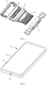
- FIG. 1 is a schematic structural diagram of a typical Type-C receptacle connector in the existing technology.
- a Type-C receptacle connector mainly includes a terminal board 01, a connecting seat 02, and a shielding cover 03.
- the terminal board 01 is provided with an inner connecting part 012 and an outer connecting part 011.
- the outer connecting part 011 is configured to be connected to a plug of a data cable.
- the inner connecting part 012 is configured to be to a circuit board.
- the connecting seat 02 is configured to fix the terminal board 01 onto the circuit board.
- Embodiments of this application provide a receptacle connector, an electronic device, and an assembly method.
- the assembly process of the receptacle connector is simple and the welding quality is high.
- an embodiment of this application provides a receptacle connector, which is applied to an electronic device such as a mobile phone, a tablet computer, a PC, a computer or a wearable device to achieve charging, data transmission, sound transmission and the like of the electronic device.
- the receptacle connector includes a terminal board.
- the terminal board is provided with a first connecting part configured to be to a circuit board of the electronic device and the terminal board is also provided with a second connecting part configured to be fitted with a plug connector.
- the first connecting part and the second connecting part are electrically connected and respectively provided at two end portions of the terminal board.
- Both the first connecting part and the second connecting part are formed by a conductor and are electrically connected through an internal line of the terminal board to achieve data or signal communication between an external data cable and an internal circuit board of the electronic device.
- the receptacle connector further includes an auxiliary member.
- the auxiliary member is detachably connected to the terminal board. An end portion of the terminal board close to the second connecting part is supported onto the circuit board through the auxiliary member.
- the auxiliary member may be a metal member. Of course, it may also be a non-metal member, such as a plastic member.
- the auxiliary member may be connected to the terminal board in a clamping manner.
- an end portion of the terminal board close to the second connecting part may be supported onto the circuit board through the auxiliary member.
- the auxiliary member can support an end portion of the terminal board away from the first connecting part, so that the second connecting part that is heavier of the terminal board can be prevented from rotating downwards to some extent, thereby preventing a weld leg for welding between the first connecting part and the circuit board from tilting up, avoiding insufficient welding between the first connecting part and the circuit board, and improving the welding quality of the terminal board and the circuit board.
- the auxiliary member and the terminal board are detachably connected.
- the auxiliary member can be dismounted from the terminal board and then assembled with a housing, so that the receptacle connector occupies a small space, thereby facilitating the flexible arrangement of other components in the electronic device.
- the receptacle connector in this application has a small thickness, thereby meeting the requirement of lightweight and thinning design for the electronic device.
- the terminal board includes a conductor and an insulator forming an integral structure, the auxiliary member is detachably connected to the insulator, and the conductor is at least partially exposed outside the insulator to form the first connecting part and the second connecting part.
- the conductor may be made of a metal material.
- the insulator may be made of a plastic material.
- the insulator and the conductor may be integrally formed through an injection molding process. While facilitating the mounting and fixation of the conductor, injection molding provides a strong bonding force, so that the connection reliability between the insulator and the conductor is high.
- the method for the connection between the conductor and the insulator is not limited to the integral injection molding process described above. They may also be connected by using various methods such as interference fit, bonding, or screwing, as long as the reliability of the connection between the two can be ensured.
- an embodiment of this application further provides a second implementation of the first aspect: the auxiliary member and the insulator are connected in a clamping manner.
- the structure connected in a clamping manner is compact and occupies a small space.
- the method for the connection between the auxiliary member and the insulator is not limited to clamping described above, and may also be bolting, or connection through a locking pin and a locking hole.
- an embodiment of this application further provides a fourth implementation of the first aspect: an outer peripheral wall of the sleeve is provided with at least two supporting walls extending outwards and respectively located on two sides of the sleeve, and the sleeve is supported onto the circuit board through the supporting walls.
- the supporting walls may be symmetrically arranged about a vertical plane where a central axis of the sleeve is located, so as to improve the stable supporting ability.
- the supporting walls on the outer wall of the sleeve may be appropriately configured according to the arrangement of the circuit board. The arrangement positions of the supporting wall avoids the arrangement positions of components and circuits on the circuit board as much as possible, so as to improve the arrangement flexibility while providing stable support.
- an embodiment of this application further provides a fifth implementation of the first aspect: a bump is provided on the surface of each supporting wall facing the circuit board, and the supporting wall is supported onto the circuit board through the bump.
- a contact surface between the bump and the circuit board may be flat.
- the supporting walls are in contact with the circuit board through the bump.
- an embodiment of this application further provides a sixth implementation of the first aspect: the receptacle connector further includes a shielding cover fixed to the insulator, and the shielding cover is configured to shield the first connecting part.
- the connection between the receptacle connector and the circuit board can be prevented from interfering with the working of external components, thereby improving the reliability of working performance of the electronic device.
- an embodiment of this application further provides an eighth implementation of the first aspect: the metal mounting member is integrally formed with the insulator through an injection molding process.
- the injection molding process enables a relatively high bonding ability to bonding between the metal mounting member and the insulator.
- the metal mounting member includes supporting bodies extending outwards from two sides of the insulator, two side walls of the shielding cover in parallel with a plugging direction are provided with bent edges, and the bent edges are welded and fixed to the supporting bodies on corresponding sides.
- a contact area between the bent edges and the supporting bodies is large, so that the welding and fixing reliability is high.
- the metal mounting member further includes a main body section, the supporting bodies are connected to two end portions of the main body section, the main body section is formed in the insulator, and the main body section is lower than the supporting bodies.
- the main body section may be a simple straight section. Of course, it may also be a non-straight section.
- the main body section may be embedded deep inside the insulator to improve the fixing reliability of the two.
- the height of the supporting bodies can meet mounting requirements of the shielding cover.
- an embodiment of this application further provides a twelfth implementation of the first aspect: a local position on a side wall of the shielding cover is further provided with a second pin configured to be plugged into the circuit board of the electronic device.
- the shielding cover and the circuit board are further fitted through the pin in a plugging manner to limit a displacement of the shielding cover along a thickness direction, thereby further improving the mounting stability of the receptacle connector and the circuit board.
- annular groove may be provided in the insulator, and an inner ring of the sealing ring is embedded into the annular groove, thereby increasing the sealing performance between the sealing ring and the housing, and the sealing performance between the sealing ring and the insulator.
- no annular groove may be provided in the insulator and the housing, and the sealing ring may be press-fitted between the housing and the insulator.
- the sealing ring can isolate a mounting space of the first connecting part, the circuit board and the like from the external environment, and only the second connecting part can be communicated with the external environment through the plugging hole in the housing, thereby preventing media in the external environment from influencing operations of other components in the housing, and improving the overall working performance of the electronic device.
- an embodiment of this application further provides an electronic device, which includes a housing and the receptacle connector according to any one of implementations above.
- the receptacle connector is mounted in the housing.
- the first connecting part is welded to the circuit board of the electronic device.
- the housing is further provided with a plugging hole at a position corresponding to the second connecting part.
- an embodiment of this application further provides a first implementation of the second aspect: the housing further includes a cylindrical section extending from a circumferential direction of the plugging hole to the receptacle connector, the second connecting part is located in the cylindrical section, and the receptacle connector and the cylindrical section are circumferentially sealed through a sealing ring.
- an embodiment of this application further provides a second implementation of the second aspect: an inner wall of an open end of the cylindrical section close to the first connecting part is further provided with a boss part extending radially and configured to limit a plugging position of a plug connector, and the second connecting part is located on an outer side of the boss part.
- the cylindrical section and the sealing ring can fully isolate the external environment from a space where the circuit board is located, and the terminal board can be supported onto the cylindrical section through the sealing ring, thereby further improving the supporting strength of an end portion where the second connecting part of the terminal board is located to improve the strength of the electronic device in use.
- the second connecting part and an external plug connector are connected in the cylindrical section in a plugging manner.
- the cylindrical section can guide the mounting of a plug connector to some extent, thereby facilitating the accurate connection between the plug connector and the receptacle connector, and improving the mounting accuracy.
- the cylindrical section can also provide auxiliary support for the plug connector, thereby preventing the plug connector from vibrating or shaking during insertion.
- an embodiment of this application further provides a third implementation of the second aspect: the boss part is an annular boss, and the sealing ring is press-fitted between the annular boss and the receptacle connector.
- the annular boss is simple in structure and can cooperate with the sealing ring to form a reliable sealing structure.
- this application further provides an assembly method for an electronic device.
- the electronic device includes the receptacle connector according to any one of implementations above.
- the assembly method includes:
- the receptacle connector is used as an implementation basis and the electronic device includes the receptacle connector described above. Therefore, the assembly method and the electronic device also have the technical effects of the receptacle connector described above.
- FIG. 1 it can be seen that a size occupied by the connecting seat in a direction perpendicular to a length of the terminal board is large.
- the connecting seat is prone to stack interference with the antenna devices, thereby affecting the mounting of the receptacle connector.
- this application further explores, conducts a greater number of tests, and proposes a technical solution that can effectively solve the technical problem above.
- FIG. 2 is a schematic structural diagram of a specific implementation of an electronic device according to an embodiment of this application.
- the electronic device 100 may be a mobile phone, a computer (such as a personal digital assistant computer, a tablet, or a laptop), a smart watch, a smart bracelet, a PAD, or the like.
- a computer such as a personal digital assistant computer, a tablet, or a laptop
- a smart watch such as a smart bracelet
- PAD PAD
- the specific form of the electronic device 100 is not specially limited in this embodiment of this application. For ease of understanding, description is made below by taking the electronic device 100 being a mobile phone as an example.
- the electronic device 100 may generally include a housing 102 and a display screen 101.
- An accommodating chamber may be formed in the housing 102.
- Various components of the electronic device 100 may be arranged in the accommodating chamber. Specific components may include a battery, a circuit board, a camera component, and the like. The arrangement and mounting methods of these components are not limited here.
- the housing 102 usually has two main functions. One is to achieve a protection function.
- the housing 102 serves as an external frame and can protect the electronic device 100.
- the other is to provide a mounting foundation. Other components may be directly or indirectly mounted onto the housing 102 to form an integral mounted body.
- the display screen 101 may be mounted onto the housing 102.
- the housing 102 may include a middle frame and a back cover, and the display screen 101 may be fixedly mounted onto the middle frame.
- the material of the housing 102 is not limited here. In specific practice, those skilled in the art can select the material based on the actual requirement. For example, the material may be a metal material, a plastic material, a ceramic material, a glass material, or the like.
- the display screen 101 may be an organic light-emitting diode display screen, a liquid crystal display screen, or the like.
- the display screen 101 may be a flexible display screen or a hard display screen.
- the flexible display screen may have a foldable function and can cooperate with the structural design of the housing 102 to achieve folding and other operations of the electronic device 100.
- the display screen 101 may be a common regular screen or an irregular screen. For example, an outer edge of the display screen 101 may be arc-shaped to form a curved screen.
- the display screen 101 may cover all areas of the front side of the electronic device 100, forming a full-screen electronic device 100.
- the display screen 101 not only has a display function, but also usually has a touch function, that is, by tapping on the display screen 101, the electronic device 100 can be operated.
- the display screen 101 may also only cover a partial area of the front side of the electronic device 100. This is also a practical option.
- the display screen 101 may have a touch function or have a display function only.
- an area of the housing 102 where the display screen 101 is not provided may be provided with human-machine operating components such as corresponding button to operate the electronic device 100.
- human-machine operating components may be provided at any position on the front side, back side, or side surfaces of the electronic device 100.
- the normal direction may also be referred to as a thickness direction.
- the lightweight and thinning design of the electronic device 100 has gradually become a trend of industry development.
- the lightweight and thinning design requires a thickness of each component in the electronic device 100 to be as small as possible to reduce a thickness of the electronic device 100 formed finally.
- the electronic device 100 is provided with a receptacle connector.
- the housing 102 is further provided with a plugging hole 103.
- An external plug connector can be inserted through the plugging hole 103 to connect to the receptacle connector, thereby achieving data transmission, power transmission (for charging the electronic device 100), sound signal transmission, and the like.
- the receptacle connector may be specifically a Type-C receptacle connector. Of course, it may also be other types of connectors such as Type-A receptacle connector or Type-B receptacle connector.
- Type-C receptacle connector As an example.
- FIG. 3 is an exploded view of a device body of a receptacle connector according to an embodiment of this application.
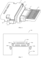
- FIG. 4 is a schematic diagram of the receptacle connector in FIG. 3 after assembled with a circuit board.
- FIG. 5 is a side view of a structure in FIG. 4 .
- the receptacle connector 106 in this application includes a terminal board, an auxiliary member 4, a sealing ring 5, and a shielding cover 2.
- the terminal board in this application includes a terminal assembly and an insulator 10.
- the terminal assembly is a conductor, usually a metal member.
- the insulator 10 may be a plastic member.
- the terminal assembly and the insulator 10 may be integrally formed through injection molding, so that the bonding force between the two is strong, the connection reliability is high, and the forming method is simple.
- the insulator 10 mainly provides a foundation for the mounting of the terminal assembly.
- the terminal board is in insulated contact with other surrounding components through the insulator 10.
- the method for the connection between the terminal assembly and the insulator 10 in the terminal board is not limited to the method described above, as long as the connection reliability between the two can be guaranteed.
- the terminal assembly and the insulator 10 may be fixed through bonding by using an adhesive.
- the terminal assembly and the insulator 10 may also be connected through interference fit, welding, or the like.
- the terminal assembly is provided with a first connecting part 11 and a second connecting part 12 exposed outside the insulator 10.
- the first connecting part 11 and the second connecting part 12 are respectively provided at two end portions of the terminal board. That is to say, both the first connecting part 11 and the second connecting part 12 are also conductors.
- the first connecting part 11 is configured to be welded to the circuit board of the electronic devices. Specifically, Weld legs of the first connecting part 11 are welded to the circuit board a one-to-one correspondence.
- the second connecting part 12 is configured to be fitted with a plug connector 105 outside the electronic device in a plugging manner.
- the specific arrangement of the first connecting part 11 and the second connecting part 12 may be determined according to the specific product, which is not limited here.
- the auxiliary member 4 is detachably connected to the terminal board.
- the terminal board is provided with a first detachable structure
- the auxiliary member 4 is provided with a second detachable structure.
- the first detachable structure can be fitted with the second detachable structure to achieve the mounting of the auxiliary member 4 onto the terminal board or the dismounting from the terminal board.
- the auxiliary member 4 is connected to the terminal board in a clamping manner. That is, one of the first detachable structure and the second detachable structure is a clamping groove, and the other is a clamping block that can slide in or out of the clamping groove. Please understand with reference to FIG. 3 .
- the auxiliary member 4 is provided with clamping blocks (not shown) that are fitted with the clamping grooves in a clamping manner.
- the auxiliary member 4 is provided with the clamping grooves and the terminal board is provided with the clamping blocks.
- the fitting of the clamping grooves and the clamping blocks makes the occupied space small.
- the method for the detachable connection between the terminal board and the auxiliary member 4 is not limited to the clamping grooves and the clamping blocks described above. Other methods such as locking pins, bolting, or locking screws may also be adopted.
- an end portion of the terminal board 1 close to the second connecting part 12 may be supported onto the circuit board 104 through the auxiliary member 4.
- the auxiliary member 4 can support an end portion of the terminal board away from the first connecting part 11, so that the second connecting part 12 that is heavier of the terminal board can be prevented from rotating downwards to some extent, thereby preventing a weld leg for welding between the first connecting part 11 and the circuit board from tilting up, avoiding insufficient welding between the first connecting part 11 and the circuit board, and improving the welding quality of the terminal board and the circuit board.
- the auxiliary member 4 and the terminal board are detachably connected.
- the auxiliary member 4 can be dismounted from the terminal board and then assembled with a housing 102, so that the receptacle connector 106 occupies a small space, thereby facilitating the flexible arrangement of other components in the electronic device.
- the receptacle connector 106 in this application has a small thickness, thereby meeting the requirement of lightweight and thinning design for the electronic device.
- the weld leg of the first connecting part 11 just comes into contact with and rests against the circuit board.
- one end of the second connecting part 12 of the terminal board may be roughly horizontal after supported onto the circuit board through the auxiliary member 4, allowing for a margin of error.
- the terminal 1 includes a conductor and an insulator 10 that form a whole, the auxiliary member 4 is detachably connected to the insulating member, and the auxiliary member 4 is connected to the insulating member but is not in contact with the conductor, thereby preventing the conductor form being damaged and ensuring the working performance of the receptacle connector 106. Moreover, machining a structure fitted with the auxiliary member 4 for dismounting on the insulator is simple.
- the auxiliary member 4 is a sleeve with an opening in at least one end.
- the sleeve may be a hollow cylinder with an opening in only one end.
- the sleeve may also be a hollow cylinder with openings in both ends. The specific implementation of the latter is shown in the drawings of this application.
- the sleeve can protect the second connecting part 12 and avoid poor device contact due to damage or contamination of the second connecting part 12 during transportation or mounting, thereby ensuring the overall performance of the electronic device.
- the sleeve may be fitted with and supported onto the circuit board to make the weld leg of the first connecting part 11 of the terminal board come into contact with and rest against the circuit board.
- the sleeve can fully protect the second connecting part 12, and the hollow structure is lightweight.
- the mounting of the sleeve with an opening in one end needs to consider a length of the second connecting part 12.
- the sleeve may be fitted with and supported onto the circuit board 104 in various ways.
- an outer peripheral wall of the sleeve is provided with at least two supporting walls extending outwards.
- the two supporting walls are respectively located on two sides of the sleeve.
- the supporting walls are roughly in parallel with the circuit board.
- the sleeve is supported onto the circuit board through the supporting walls.
- An extension length of the supporting walls may be determined according to the specific application environment. In this application, since the sleeve is fitted with and supported onto the circuit board through the supporting walls, only the manufacturing accuracy of the supporting walls needs to be considered during manufacturing. In addition, since the supporting walls are provided on the two sides of the sleeve, the supporting stability on the two sides is high.
- the surface of the circuit board is usually provided with a circuit or other components. To improve the supporting stability as much as possible, this application further improves the supporting walls as follows.
- each supporting wall facing the circuit board is further provided with a bump 411, and the supporting wall is fitted with and supported onto the circuit board through the bump 411.
- a contact surface between the bump 411 and the circuit board may be flat. In this way, the wear of the circuit board caused by the bump 411 can be minimized.
- the circuit board 104 is provided with a notch 104c at a position corresponding to the second connecting part 12, and a part of the sleeve along a thickness direction is located in the notch 104c.
- the arrangement of the sleeve and the circuit board can be optimized, and an internal space of the housing can be fully utilized.
- the receptacle connector 106 further includes a shielding cover 2.
- the shielding cover 2 is mainly configured to shield the first connecting part 11 to achieve an electromagnetic shielding effect.
- the shielding cover 2 is usually a metal component.
- a shape of the shielding cover 2 is mainly determined according to a specific structure of the circuit board and the terminal board.
- the shielding cover 2 includes a top wall and three side walls connected to the top wall to form two openings facing a side of the circuit board and facing a side of the first connecting part 11.
- a structure of the shielding cover 2 is not limited to the one described herein.
- the shielding cover 2 is fixed to the terminal board.
- the shielding cover 2 is fixed to a position where the terminal assembly of the terminal board is not located.
- the shielding cover 2 may be pre-assembled with the terminal board to form a whole, and then assembled together on the circuit board 104. In this way, the assembly efficiency of the electronic device can be improved.
- a metal mounting member 3 is fixed in the insulator of the receptacle connector 106.
- the shielding cover 2 is fixedly connected to the metal mounting member 3 through welding.
- the metal mounting member 3 may be fixed to the insulator 10 through an injection molding process.
- injection molding may also be performed in two steps. Firstly, the conductor is injection-molded with one part of the insulator 10 to form the first terminal board, and then the first terminal board is integrally formed with the metal mounting member 3 through the injection molding process.
- the method of fixing the metal mounting member 3 to the terminal board through injection molding can ensure the firmness.
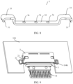
- the metal mounting member 3 includes a main body section 32 and supporting bodies 33 located at different heights.
- the positions of the supporting bodies 33 are higher than the position of the main body section 32.
- the main body section 32 may be embedded deep inside the insulator 10 to improve the fixing reliability.
- the height of the supporting bodies 33 can meet mounting requirements of the shielding cover 2.
- FIG. 7 further shows a welding area 1041 on the circuit board for butt welding with the weld leg of the first connecting part 11. Welding pieces corresponding to weld legs one to one are provided in the welding area 1041.
- the two side walls of the shielding cover 2 are provided with bent edges 21.
- the bent edges 21 are welded and fixed to the supporting bodies on corresponding sides.
- the bent edges 21 are in surface-surface contact with the supporting bodies, and a contact area is large, thereby improving the welding reliability.
- the shielding cover 2 and the supporting bodies may be fixed through laser welding. Of course, they may also be fixed through other welding methods.
- a second pin 22 is further provided at a local position on a side wall of the shielding cover 2, and the second pin 22 is configured to be plugged into the circuit board of the electronic device.
- the circuit board is provided with a second jack 104a, and the second pin 22 is plugged into the second jack 104a.
- fixing the shielding cover 2 to the circuit board in a plugging manner can further improve the fixing and bonding strength between the receptacle connector 106 and the circuit board.
- the receptacle connector 106 is further provided with a sealing ring 5.
- the sealing ring 5 hermetically sleeves the insulator 10 to circumferentially seal it.
- the sealing ring 5 is mainly configured to achieve circumferential sealing between the insulator 10 and the housing 102.
- the sealing ring 5 further includes an annular part that circumferentially seals the housing 102.
- the annular part may be embedded to seal the housing 102. That is, the annular part is partially located in an annular sealing groove in the housing 102. Of course, the annular part may also be directly press-fitted to seal the housing 102.
- the first connecting part 11 and the second connecting part 12 are located on two sides of the sealing ring 5.
- the second connecting part 12 is located on a side of the housing 102 close to the plugging hole.
- the sealing ring 5 circumferentially seals the middle frame.
- the housing 102 further includes a cylindrical section 1021 extending from a circumferential direction of the plugging hole to the receptacle connector 106.
- the second connecting part 12 is located in the cylindrical section 1021.
- the sealing ring 5 is provided between the receptacle connector 106 and the cylindrical section 1021. That is, the receptacle connector 106 and the cylindrical section 1021 are circumferentially sealed through the sealing ring 5.
- the cylindrical section 1021 and the sealing ring 5 can fully isolate the external environment from a space where the circuit board is located, and the terminal board can be supported onto the cylindrical section 1021 through the sealing ring 5, thereby further improving the supporting strength of an end portion where the second connecting part 12 of the terminal board is located to improve the strength of the electronic device in use.
- the second connecting part 12 and the external plug connector 105 are connected in the cylindrical section 1021 in a plugging manner.
- the cylindrical section 1021 can guide the mounting of the plug connector to some extent, thereby facilitating the accurate connection between the plug connector 105 and the receptacle connector 106, and improving the mounting accuracy.
- the cylindrical section 1021 can also provide auxiliary support for the plug connector 105, thereby preventing the plug connector 105 from vibrating or shaking during insertion.
- a local position on the circuit board facing the plugging hole is provided with a notch.
- the cylindrical section 1021 is located in the notch, and the second connecting part 12 stretches into the notch.
- the cylindrical section 1021 only occupies an area of the position of the notch in the circuit board, thereby minimizing a space occupied in the housing 102, and facilitating the arrangement of the circuit board in the housing 102.
- an inner wall of an open end of the cylindrical section 1021 close to the first connecting part 11 is further provided with a boss part 1022 configured to limit the plugging position of the plug connector 105.
- the second connecting part 12 is located on an outer side of the boss part 1022. The boss part 1022 can limit the maximum plugging position of the plug connector 105, thereby avoiding the damage to the receptacle connector 106 and the circuit board caused by excessive plugging, and improving the safety of the electronic device in use.
- the boss part is an annular boss
- the sealing ring 5 is press-fitted between the annular boss and the receptacle connector 106. In this way, 360-degree sealing can be achieved, and the sealing effect is good.
- This application further provides an assembly method for an electronic device.
- the assembly method is mainly based on the receptacle connector 106 described above in this application.
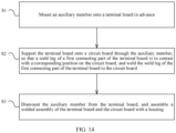
- the assembly method includes the following steps:
- the shielding cover 2 of the receptacle connector 106 may be fixed to the terminal board to form a whole in advance before step S2. Of course, it may also be fixedly connected to the circuit board or/and the terminal board in step S2.
- the sealing ring 5 may be positioned and connected to the terminal board before step S2.
- FIG. 10 is a schematic diagram of the receptacle connector 106 before assembled with the housing 102.
- FIG. 11 is a schematic diagram after the two are assembled.
- the receptacle connector 106 is used as an implementation basis and the electronic device includes the receptacle connector 106 described above. Therefore, the assembly method and the electronic device also have the technical effects of the receptacle connector 106 described above.
Landscapes
- Engineering & Computer Science (AREA)
- Manufacturing & Machinery (AREA)
- Coupling Device And Connection With Printed Circuit (AREA)
Abstract
Description
- This application claims priority to
Chinese Patent Application No. 202211064415.6, filed with the China National Intellectual Property Administration on September 1, 2022 - Embodiments of this application relate to the technical field of connectors, and in particular to a receptacle connector, an electronic device, and an assembly method.
- At present, most electronic devices are provided with receptacle connectors, such as Type-A receptacle connectors or Type-C receptacle connectors, and other different types of connectors. The main function of the receptacle connector is to be connected to a plug of an external data cable to achieve charging, data transmission, sound signal transmission, and the like.
- Among various types of receptacle connectors, Type-C is widely applied. Please refer to
FIG. 1. FIG. 1 is a schematic structural diagram of a typical Type-C receptacle connector in the existing technology. - At present, a Type-C receptacle connector mainly includes a
terminal board 01, a connectingseat 02, and ashielding cover 03. Theterminal board 01 is provided with an inner connectingpart 012 and an outer connectingpart 011. The outer connectingpart 011 is configured to be connected to a plug of a data cable. The inner connectingpart 012 is configured to be to a circuit board. The connectingseat 02 is configured to fix theterminal board 01 onto the circuit board. When the Type-C receptacle connector with this structure is welded onto the circuit board, it is difficult to locate a welding position between the Type-C receptacle connector and the circuit board. As a result, the welding quality is not high, and there is a phenomenon of insufficient welding. - Therefore, how to solve at least one of the technical defects described above is still an urgent technical problem that needs to be solved by those skilled in the art.
- Embodiments of this application provide a receptacle connector, an electronic device, and an assembly method. The assembly process of the receptacle connector is simple and the welding quality is high.
- According to a first aspect, an embodiment of this application provides a receptacle connector, which is applied to an electronic device such as a mobile phone, a tablet computer, a PC, a computer or a wearable device to achieve charging, data transmission, sound transmission and the like of the electronic device. In this application, the receptacle connector includes a terminal board. The terminal board is provided with a first connecting part configured to be to a circuit board of the electronic device and the terminal board is also provided with a second connecting part configured to be fitted with a plug connector. The first connecting part and the second connecting part are electrically connected and respectively provided at two end portions of the terminal board. Both the first connecting part and the second connecting part are formed by a conductor and are electrically connected through an internal line of the terminal board to achieve data or signal communication between an external data cable and an internal circuit board of the electronic device. The receptacle connector further includes an auxiliary member. The auxiliary member is detachably connected to the terminal board. An end portion of the terminal board close to the second connecting part is supported onto the circuit board through the auxiliary member. The auxiliary member may be a metal member. Of course, it may also be a non-metal member, such as a plastic member. The auxiliary member may be connected to the terminal board in a clamping manner.
- In this application, an end portion of the terminal board close to the second connecting part may be supported onto the circuit board through the auxiliary member. In other words, in this application, the auxiliary member can support an end portion of the terminal board away from the first connecting part, so that the second connecting part that is heavier of the terminal board can be prevented from rotating downwards to some extent, thereby preventing a weld leg for welding between the first connecting part and the circuit board from tilting up, avoiding insufficient welding between the first connecting part and the circuit board, and improving the welding quality of the terminal board and the circuit board. Moreover, in this application, the auxiliary member and the terminal board are detachably connected. After the terminal board and the circuit board are welded and fixed, the auxiliary member can be dismounted from the terminal board and then assembled with a housing, so that the receptacle connector occupies a small space, thereby facilitating the flexible arrangement of other components in the electronic device. In addition, the receptacle connector in this application has a small thickness, thereby meeting the requirement of lightweight and thinning design for the electronic device.
- Based on the first aspect, an embodiment of this application further provides a first implementation of the first aspect: the terminal board includes a conductor and an insulator forming an integral structure, the auxiliary member is detachably connected to the insulator, and the conductor is at least partially exposed outside the insulator to form the first connecting part and the second connecting part. The conductor may be made of a metal material. The insulator may be made of a plastic material. The insulator and the conductor may be integrally formed through an injection molding process. While facilitating the mounting and fixation of the conductor, injection molding provides a strong bonding force, so that the connection reliability between the insulator and the conductor is high.
- Of course, the method for the connection between the conductor and the insulator is not limited to the integral injection molding process described above. They may also be connected by using various methods such as interference fit, bonding, or screwing, as long as the reliability of the connection between the two can be ensured.
- Based on the first implementation of the first aspect, an embodiment of this application further provides a second implementation of the first aspect: the auxiliary member and the insulator are connected in a clamping manner. The structure connected in a clamping manner is compact and occupies a small space. Of course, the method for the connection between the auxiliary member and the insulator is not limited to clamping described above, and may also be bolting, or connection through a locking pin and a locking hole.
- Based on any one of the first implementation to the second implementation of the first aspect, an embodiment of this application further provide a third implementation of the first aspect: the auxiliary member includes a sleeve with an opening in at least one end, and the second connecting part is at least partially located in an annular peripheral wall of the sleeve when the sleeve is fitted onto the terminal board through the opening. The sleeve may be provided with only one opening, with the other end closed, so that before the receptacle connector is assembled with the housing, the second connecting part can be located in a relatively closed space, thereby providing strong protection for the second connecting part. Of course, the sleeve may also be provided with openings in both ends. When the sleeve is assembled, there is no need to consider the length of the second connecting part, so that the assembly flexibility is high. In addition, the structure of the sleeve is simple to form and low in material consumption, thereby reducing the use cost.
- Based on the third implementation of the first aspect, an embodiment of this application further provides a fourth implementation of the first aspect: an outer peripheral wall of the sleeve is provided with at least two supporting walls extending outwards and respectively located on two sides of the sleeve, and the sleeve is supported onto the circuit board through the supporting walls. The supporting walls may be symmetrically arranged about a vertical plane where a central axis of the sleeve is located, so as to improve the stable supporting ability. The supporting walls on the outer wall of the sleeve may be appropriately configured according to the arrangement of the circuit board. The arrangement positions of the supporting wall avoids the arrangement positions of components and circuits on the circuit board as much as possible, so as to improve the arrangement flexibility while providing stable support.
- Based on the fourth implementation of the first aspect, an embodiment of this application further provides a fifth implementation of the first aspect: a bump is provided on the surface of each supporting wall facing the circuit board, and the supporting wall is supported onto the circuit board through the bump. A contact surface between the bump and the circuit board may be flat. The supporting walls are in contact with the circuit board through the bump. Compared with large-area surface contact, the contact between the bump and the circuit board in this application is equivalent to point-surface contact, so that a contact area is small, thereby reducing factors that affect the supporting strength.
- Based on any one of the first implementation to the fifth implementation of the first aspect, an embodiment of this application further provides a sixth implementation of the first aspect: the receptacle connector further includes a shielding cover fixed to the insulator, and the shielding cover is configured to shield the first connecting part. In this way, the connection between the receptacle connector and the circuit board can be prevented from interfering with the working of external components, thereby improving the reliability of working performance of the electronic device.
- Based on the sixth implementation of the first aspect, an embodiment of this application further provides a seventh implementation of the first aspect: the receptacle connector further includes a metal mounting member fixed to the insulator, and the shielding cover is welded to the metal mounting member. The shielding cover is usually made of a metal material. The reliability of welding and fixing of the metal material and the metal mounting member is high.
- Based on the seventh implementation of the first aspect, an embodiment of this application further provides an eighth implementation of the first aspect: the metal mounting member is integrally formed with the insulator through an injection molding process. The injection molding process enables a relatively high bonding ability to bonding between the metal mounting member and the insulator.
- Of course, the method for the connection between the shielding cover and the insulator is not limited to the welding method described above, and may also be bonding, screwing, interference fit, or the like.
- Based on the seven implementation or the eighth implementation of the first aspect, an embodiment of this application further provides a ninth implementation of the first aspect: the metal mounting member includes supporting bodies extending outwards from two sides of the insulator, two side walls of the shielding cover in parallel with a plugging direction are provided with bent edges, and the bent edges are welded and fixed to the supporting bodies on corresponding sides. A contact area between the bent edges and the supporting bodies is large, so that the welding and fixing reliability is high.
- Based on the ninth implementation of the first aspect, an embodiment of this application further provides a tenth implementation of the first aspect: the metal mounting member further includes a main body section, the supporting bodies are connected to two end portions of the main body section, the main body section is formed in the insulator, and the main body section is lower than the supporting bodies. The main body section may be a simple straight section. Of course, it may also be a non-straight section. The main body section may be embedded deep inside the insulator to improve the fixing reliability of the two. The height of the supporting bodies can meet mounting requirements of the shielding cover.
- Based on the tenth implementation or the ninth implementation of the first aspect, an embodiment of this application further provides an eleventh implementation of the first aspect: each supporting body is further provided with a first pin bent towards a side away from the shielding cover and configured to be plugged into the circuit board of the electronic device. Correspondingly, a first jack is provided in the circuit board, and the first pin is plugged and fixed into the first jack to improve the bonding strength between the supporting bodies and the circuit board along the thickness direction.
- Based on any one of the sixth implementation to the eleventh implementation of the first aspect, an embodiment of this application further provides a twelfth implementation of the first aspect: a local position on a side wall of the shielding cover is further provided with a second pin configured to be plugged into the circuit board of the electronic device. In this example, the shielding cover and the circuit board are further fitted through the pin in a plugging manner to limit a displacement of the shielding cover along a thickness direction, thereby further improving the mounting stability of the receptacle connector and the circuit board.
- Based on any one of the first implementation to the twelfth implementation of the first aspect, an embodiment of this application further provides a twelfth implementation of the first aspect: the receptacle connector further includes a sealing ring, the sealing ring hermetically sleeves the insulator, the first connecting part and the second connecting part are located on two sides of the sealing ring, and the sealing ring includes an annular part that circumferentially seals a housing of the electronic device. The sealing ring may be an O-ring. An outer ring of the sealing ring may be embedded into an annular mounting groove in the housing. Of course, an annular groove may be provided in the insulator, and an inner ring of the sealing ring is embedded into the annular groove, thereby increasing the sealing performance between the sealing ring and the housing, and the sealing performance between the sealing ring and the insulator. Of course, no annular groove may be provided in the insulator and the housing, and the sealing ring may be press-fitted between the housing and the insulator.
- In this application, the sealing ring can isolate a mounting space of the first connecting part, the circuit board and the like from the external environment, and only the second connecting part can be communicated with the external environment through the plugging hole in the housing, thereby preventing media in the external environment from influencing operations of other components in the housing, and improving the overall working performance of the electronic device.
- According to a second aspect, an embodiment of this application further provides an electronic device, which includes a housing and the receptacle connector according to any one of implementations above. The receptacle connector is mounted in the housing. The first connecting part is welded to the circuit board of the electronic device. The housing is further provided with a plugging hole at a position corresponding to the second connecting part.
- Based on the second aspect, an embodiment of this application further provides a first implementation of the second aspect: the housing further includes a cylindrical section extending from a circumferential direction of the plugging hole to the receptacle connector, the second connecting part is located in the cylindrical section, and the receptacle connector and the cylindrical section are circumferentially sealed through a sealing ring.
- Based on the first implementation of the second aspect, an embodiment of this application further provides a second implementation of the second aspect: an inner wall of an open end of the cylindrical section close to the first connecting part is further provided with a boss part extending radially and configured to limit a plugging position of a plug connector, and the second connecting part is located on an outer side of the boss part.
- The cylindrical section and the sealing ring can fully isolate the external environment from a space where the circuit board is located, and the terminal board can be supported onto the cylindrical section through the sealing ring, thereby further improving the supporting strength of an end portion where the second connecting part of the terminal board is located to improve the strength of the electronic device in use. Further, the second connecting part and an external plug connector are connected in the cylindrical section in a plugging manner. By setting an inner diameter of the cylindrical section, the cylindrical section can guide the mounting of a plug connector to some extent, thereby facilitating the accurate connection between the plug connector and the receptacle connector, and improving the mounting accuracy. In addition, the cylindrical section can also provide auxiliary support for the plug connector, thereby preventing the plug connector from vibrating or shaking during insertion.
- Based on the second implementation of the second aspect, an embodiment of this application further provides a third implementation of the second aspect: the boss part is an annular boss, and the sealing ring is press-fitted between the annular boss and the receptacle connector. The annular boss is simple in structure and can cooperate with the sealing ring to form a reliable sealing structure.
- According to a third aspect, this application further provides an assembly method for an electronic device. The electronic device includes the receptacle connector according to any one of implementations above. The assembly method includes:
- mounting the auxiliary member onto the terminal board in advance, supporting an end portion of the terminal board away from the first connecting part onto the circuit board through the auxiliary member, so that a weld leg of the first connecting part of the terminal board are in contact with a corresponding position on the circuit board, and welding the weld leg of the first connecting part of the terminal board to the circuit board;
- dismounting the auxiliary member from the terminal board, and assembling a welded assembly formed by the terminal board and the circuit board with the housing of the electronic device.
- In the assembly method in this application, the receptacle connector is used as an implementation basis and the electronic device includes the receptacle connector described above. Therefore, the assembly method and the electronic device also have the technical effects of the receptacle connector described above.
-
-
FIG. 1 is a schematic structural diagram of a typical receptacle connector in the existing technology; -
FIG. 2 is a schematic structural diagram of a specific implementation of an electronic device according to an embodiment of this application; -
FIG. 3 is an exploded view of a device body of a receptacle connector according to an embodiment of this application; -
FIG. 4 is a schematic diagram of the receptacle connector inFIG. 3 after assembled with a circuit board; -
FIG. 5 is a side view of a structure inFIG. 4 ; -
FIG. 6 is a schematic structural diagram of the receptacle connector inFIG. 4 without an auxiliary member; -
FIG. 7 is a top view of a circuit board inFIG. 4 ; -
FIG. 8 is a schematic structural diagram of a metal mounting member inFIG. 3 ; -
FIG. 9 is a schematic structural diagram of the receptacle connector inFIG. 4 after welded to a circuit board, with an auxiliary member removed; -
FIG. 10 is a schematic diagram of the structure inFIG. 9 before assembled with a housing; -
FIG. 11 is a general assembly diagram of the structure inFIG. 10 after assembling; -
FIG. 12 is a cross-sectional view in a direction of A-A inFIG. 11 ; -
FIG. 13 is a schematic diagram of the structure inFIG. 12 after a plug connector is inserted; and -
FIG. 14 is a flowchart of an assembly method for an electronic device according to an embodiment of this application. - Description of reference signs in
FIG. 1 :
01-terminal board, 011-outer connecting part, 012-inner connecting part; and 02-connecting seat. - Description of reference signs in
FIG. 2 to FIG. 13 : - 100-electronic device, 101-display screen, 102-housing, 1021-cylindrical section; 1022-boss part; 103-plugging hole; 104-circuit board; 104a-first jack; 104b-second jack; 104c-notch; 105-plug connector; 106-receptacle connector;
- 1-terminal board; 10-insulator; 11-first connecting part; 12-second connecting part; 13-clamping groove; 2-shielding cover; 21-bent edge; 22-second pin; 3-metal mounting member; 31-first pin; 32-main body section; 33-supporting body; 4-auxiliary member; 41-supporting wall; 411-bump; and 5-sealing ring
- Aiming at the problem of poor welding quality of the receptacle connector after assembled and welded onto the circuit board in the background, this application conducts research. It is found that the center of gravity of the receptacle connector shown in
FIG. 1 is located ahead of a weld leg supporting point on the inner connecting part, a seesaw pattern is formed after assembled with the circuit board and one side of the outer connecting part sinks, so that the weld leg of the inner connecting part still tilts up during welding, causing insufficient welding and affecting charging and data transmission functions. - In addition, from
FIG. 1 , it can be seen that a size occupied by the connecting seat in a direction perpendicular to a length of the terminal board is large. When there are many antenna devices arranged in the receptacle connector of the electronic device, the connecting seat is prone to stack interference with the antenna devices, thereby affecting the mounting of the receptacle connector. - Based on the research finding, this application further explores, conducts a greater number of tests, and proposes a technical solution that can effectively solve the technical problem above.
- To enable those skilled in the art to better understand the technical solutions of this application, this application will be further described in detail below in combination with the specific embodiments with reference to the drawings.
- Please refer to
FIG. 2. FIG. 2 is a schematic structural diagram of a specific implementation of an electronic device according to an embodiment of this application. - In this application, the
electronic device 100 may be a mobile phone, a computer (such as a personal digital assistant computer, a tablet, or a laptop), a smart watch, a smart bracelet, a PAD, or the like. The specific form of theelectronic device 100 is not specially limited in this embodiment of this application. For ease of understanding, description is made below by taking theelectronic device 100 being a mobile phone as an example. - Referring to
FIG. 2 , theelectronic device 100 may generally include ahousing 102 and adisplay screen 101. An accommodating chamber may be formed in thehousing 102. Various components of theelectronic device 100 may be arranged in the accommodating chamber. Specific components may include a battery, a circuit board, a camera component, and the like. The arrangement and mounting methods of these components are not limited here. - The
housing 102 usually has two main functions. One is to achieve a protection function. Thehousing 102 serves as an external frame and can protect theelectronic device 100. The other is to provide a mounting foundation. Other components may be directly or indirectly mounted onto thehousing 102 to form an integral mounted body. Thedisplay screen 101 may be mounted onto thehousing 102. In some embodiments, thehousing 102 may include a middle frame and a back cover, and thedisplay screen 101 may be fixedly mounted onto the middle frame. The material of thehousing 102 is not limited here. In specific practice, those skilled in the art can select the material based on the actual requirement. For example, the material may be a metal material, a plastic material, a ceramic material, a glass material, or the like. - The
display screen 101 may be an organic light-emitting diode display screen, a liquid crystal display screen, or the like. Thedisplay screen 101 may be a flexible display screen or a hard display screen. The flexible display screen may have a foldable function and can cooperate with the structural design of thehousing 102 to achieve folding and other operations of theelectronic device 100. Thedisplay screen 101 may be a common regular screen or an irregular screen. For example, an outer edge of thedisplay screen 101 may be arc-shaped to form a curved screen. - The
display screen 101 may be provided on a front side of theelectronic device 100, may be provided on a back side of theelectronic device 100, or may be provided on both the front side and back side of theelectronic device 100. The front side of theelectronic device 100 may be understood as a side facing the user when using theelectronic device 100, i.e., the side marked withreference number 101 inFIG. 2 . The back side of theelectronic device 100 may be understood as the side facing away from the user when using theelectronic device 100. - Taking the front side of the
electronic device 100 as an example, in terms of arrangement range, thedisplay screen 101 may cover all areas of the front side of theelectronic device 100, forming a full-screenelectronic device 100. In this case, thedisplay screen 101 not only has a display function, but also usually has a touch function, that is, by tapping on thedisplay screen 101, theelectronic device 100 can be operated. Alternatively, thedisplay screen 101 may also only cover a partial area of the front side of theelectronic device 100. This is also a practical option. In this case, thedisplay screen 101 may have a touch function or have a display function only. It is to be understood that when it has a display function only, an area of thehousing 102 where thedisplay screen 101 is not provided may be provided with human-machine operating components such as corresponding button to operate theelectronic device 100. These human-machine operating components may be provided at any position on the front side, back side, or side surfaces of theelectronic device 100. - Taking a direction perpendicular to a plane where the
display screen 101 is located as a normal direction of thedisplay screen 101, dimensions of theelectronic device 100 and components in theelectronic device 100 in the normal direction may be referred to as thickness. Correspondingly, the normal direction may also be referred to as a thickness direction. At present, with the continuous improvement of user demands, the lightweight and thinning design of theelectronic device 100 has gradually become a trend of industry development. The lightweight and thinning design requires a thickness of each component in theelectronic device 100 to be as small as possible to reduce a thickness of theelectronic device 100 formed finally. - The
electronic device 100 is provided with a receptacle connector. Thehousing 102 is further provided with a plugginghole 103. An external plug connector can be inserted through the plugginghole 103 to connect to the receptacle connector, thereby achieving data transmission, power transmission (for charging the electronic device 100), sound signal transmission, and the like. - This application provides a receptacle connector. The receptacle connector may be specifically a Type-C receptacle connector. Of course, it may also be other types of connectors such as Type-A receptacle connector or Type-B receptacle connector. The technical solutions and technical effects will be continuously introduced below by taking a Type-C receptacle connector as an example.
- Please refer to
FIG. 3 to FIG. 5 .FIG. 3 is an exploded view of a device body of a receptacle connector according to an embodiment of this application.FIG. 4 is a schematic diagram of the receptacle connector inFIG. 3 after assembled with a circuit board.FIG. 5 is a side view of a structure inFIG. 4 . - In an example, the
receptacle connector 106 in this application includes a terminal board, anauxiliary member 4, a sealingring 5, and a shieldingcover 2. - The terminal board in this application includes a terminal assembly and an insulator 10. The terminal assembly is a conductor, usually a metal member. The insulator 10 may be a plastic member. The terminal assembly and the insulator 10 may be integrally formed through injection molding, so that the bonding force between the two is strong, the connection reliability is high, and the forming method is simple. The insulator 10 mainly provides a foundation for the mounting of the terminal assembly. Moreover, the terminal board is in insulated contact with other surrounding components through the insulator 10.
- Of course, in this application, the method for the connection between the terminal assembly and the insulator 10 in the terminal board is not limited to the method described above, as long as the connection reliability between the two can be guaranteed. For example, the terminal assembly and the insulator 10 may be fixed through bonding by using an adhesive. Alternatively, the terminal assembly and the insulator 10 may also be connected through interference fit, welding, or the like.
- The terminal assembly is provided with a first connecting
part 11 and a second connectingpart 12 exposed outside the insulator 10. The first connectingpart 11 and the second connectingpart 12 are respectively provided at two end portions of the terminal board. That is to say, both the first connectingpart 11 and the second connectingpart 12 are also conductors. The first connectingpart 11 is configured to be welded to the circuit board of the electronic devices. Specifically, Weld legs of the first connectingpart 11 are welded to the circuit board a one-to-one correspondence. The second connectingpart 12 is configured to be fitted with aplug connector 105 outside the electronic device in a plugging manner. The specific arrangement of the first connectingpart 11 and the second connectingpart 12 may be determined according to the specific product, which is not limited here. - In this application, the
auxiliary member 4 is detachably connected to the terminal board. In other words, the terminal board is provided with a first detachable structure, and theauxiliary member 4 is provided with a second detachable structure. The first detachable structure can be fitted with the second detachable structure to achieve the mounting of theauxiliary member 4 onto the terminal board or the dismounting from the terminal board. In an example, theauxiliary member 4 is connected to the terminal board in a clamping manner. That is, one of the first detachable structure and the second detachable structure is a clamping groove, and the other is a clamping block that can slide in or out of the clamping groove. Please understand with reference toFIG. 3 . It shows a specific example of arrangement of the clampinggroove 13 on the terminal board. Left and right side walls of the terminal board extending along a plugging direction are provided with clampinggrooves 13. Correspondingly, theauxiliary member 4 is provided with clamping blocks (not shown) that are fitted with the clamping grooves in a clamping manner. Those skilled in the art shall understand that it is also acceptable that theauxiliary member 4 is provided with the clamping grooves and the terminal board is provided with the clamping blocks. The fitting of the clamping grooves and the clamping blocks makes the occupied space small. Of course, the method for the detachable connection between the terminal board and theauxiliary member 4 is not limited to the clamping grooves and the clamping blocks described above. Other methods such as locking pins, bolting, or locking screws may also be adopted. - In this application, an end portion of the
terminal board 1 close to the second connectingpart 12 may be supported onto thecircuit board 104 through theauxiliary member 4. In other words, in this application, theauxiliary member 4 can support an end portion of the terminal board away from the first connectingpart 11, so that the second connectingpart 12 that is heavier of the terminal board can be prevented from rotating downwards to some extent, thereby preventing a weld leg for welding between the first connectingpart 11 and the circuit board from tilting up, avoiding insufficient welding between the first connectingpart 11 and the circuit board, and improving the welding quality of the terminal board and the circuit board. Moreover, in this application, theauxiliary member 4 and the terminal board are detachably connected. After the terminal board and the circuit board are welded and fixed, theauxiliary member 4 can be dismounted from the terminal board and then assembled with ahousing 102, so that thereceptacle connector 106 occupies a small space, thereby facilitating the flexible arrangement of other components in the electronic device. In addition, thereceptacle connector 106 in this application has a small thickness, thereby meeting the requirement of lightweight and thinning design for the electronic device. - Theoretically, when the terminal board is in a horizontal state, the weld leg of the first connecting
part 11 just comes into contact with and rests against the circuit board. Of course, considering factors such as assembly errors, one end of the second connectingpart 12 of the terminal board may be roughly horizontal after supported onto the circuit board through theauxiliary member 4, allowing for a margin of error. - As described above, the
terminal 1 includes a conductor and an insulator 10 that form a whole, theauxiliary member 4 is detachably connected to the insulating member, and theauxiliary member 4 is connected to the insulating member but is not in contact with the conductor, thereby preventing the conductor form being damaged and ensuring the working performance of thereceptacle connector 106. Moreover, machining a structure fitted with theauxiliary member 4 for dismounting on the insulator is simple. - Please refer to
FIG. 3 andFIG. 4 again. In this application, theauxiliary member 4 is a sleeve with an opening in at least one end. In other words, the sleeve may be a hollow cylinder with an opening in only one end. Of course, the sleeve may also be a hollow cylinder with openings in both ends. The specific implementation of the latter is shown in the drawings of this application. When thereceptacle connector 106 is manufactured but not yet assembled with the circuit board, the sleeve is fitted over the second connectingpart 12 of the terminal board. Of course, the second connectingpart 12 may be partially or fully located in the sleeve, and the optimal state is that the second connectingpart 12 is fully located in the sleeve. In this way, the sleeve can protect the second connectingpart 12 and avoid poor device contact due to damage or contamination of the second connectingpart 12 during transportation or mounting, thereby ensuring the overall performance of the electronic device. When thereceptacle connector 106 is mounted with the circuit board, the sleeve may be fitted with and supported onto the circuit board to make the weld leg of the first connectingpart 11 of the terminal board come into contact with and rest against the circuit board. - The sleeve can fully protect the second connecting
part 12, and the hollow structure is lightweight. - Compared to the sleeve with openings in two ends, the mounting of the sleeve with an opening in one end needs to consider a length of the second connecting
part 12. - The sleeve may be fitted with and supported onto the
circuit board 104 in various ways. In a specific embodiment, an outer peripheral wall of the sleeve is provided with at least two supporting walls extending outwards. The two supporting walls are respectively located on two sides of the sleeve. The supporting walls are roughly in parallel with the circuit board. The sleeve is supported onto the circuit board through the supporting walls. An extension length of the supporting walls may be determined according to the specific application environment. In this application, since the sleeve is fitted with and supported onto the circuit board through the supporting walls, only the manufacturing accuracy of the supporting walls needs to be considered during manufacturing. In addition, since the supporting walls are provided on the two sides of the sleeve, the supporting stability on the two sides is high. - The surface of the circuit board is usually provided with a circuit or other components. To improve the supporting stability as much as possible, this application further improves the supporting walls as follows.
- Please refer to
FIG. 5 again. In this application, the surface of each supporting wall facing the circuit board is further provided with abump 411, and the supporting wall is fitted with and supported onto the circuit board through thebump 411. A contact surface between thebump 411 and the circuit board may be flat. In this way, the wear of the circuit board caused by thebump 411 can be minimized. - Please refer to
FIG. 7 . In this application, thecircuit board 104 is provided with anotch 104c at a position corresponding to the second connectingpart 12, and a part of the sleeve along a thickness direction is located in thenotch 104c. In this way, the arrangement of the sleeve and the circuit board can be optimized, and an internal space of the housing can be fully utilized. - Please understand with reference to
FIG. 6 and FIG. 7 . In this application, thereceptacle connector 106 further includes a shieldingcover 2. The shieldingcover 2 is mainly configured to shield the first connectingpart 11 to achieve an electromagnetic shielding effect. The shieldingcover 2 is usually a metal component. A shape of the shieldingcover 2 is mainly determined according to a specific structure of the circuit board and the terminal board. In this application, the shieldingcover 2 includes a top wall and three side walls connected to the top wall to form two openings facing a side of the circuit board and facing a side of the first connectingpart 11. Of course, a structure of the shieldingcover 2 is not limited to the one described herein. In this application, the shieldingcover 2 is fixed to the terminal board. Of course, the shieldingcover 2 is fixed to a position where the terminal assembly of the terminal board is not located. - In this application, the shielding
cover 2 may be pre-assembled with the terminal board to form a whole, and then assembled together on thecircuit board 104. In this way, the assembly efficiency of the electronic device can be improved. - Please refer to
FIG. 8 . In this application, ametal mounting member 3 is fixed in the insulator of thereceptacle connector 106. The shieldingcover 2 is fixedly connected to themetal mounting member 3 through welding. Themetal mounting member 3 may be fixed to the insulator 10 through an injection molding process. For example, when the insulator 10 is injection-molded, the conductor and themetal mounting member 3 may be fixed at the same time. Of course, injection molding may also be performed in two steps. Firstly, the conductor is injection-molded with one part of the insulator 10 to form the first terminal board, and then the first terminal board is integrally formed with themetal mounting member 3 through the injection molding process. - The method of fixing the
metal mounting member 3 to the terminal board through injection molding can ensure the firmness. - Of course, the method for fixing the shielding
cover 2 to the terminal board is not limited to welding described above, and may also be riveting, screwing, interference fit, injection molding, and the like. - The closer the
metal mounting member 3 is to an upper surface of the insulator 10, the poorer the fixing performance. To improve the fixing reliability of themetal mounting member 3, in this application, themetal mounting member 3 includes a main body section 32 and supportingbodies 33 located at different heights. The positions of the supportingbodies 33 are higher than the position of the main body section 32. The main body section 32 may be embedded deep inside the insulator 10 to improve the fixing reliability. The height of the supportingbodies 33 can meet mounting requirements of the shieldingcover 2. - To improve the bonding strength between the main body section 32 and the insulator 10, the main body section 32 may be further provided with a through hole 32a.
- Please understand with reference to
FIG. 7 andFIG. 8 . Each supportingbody 33 is further provided with afirst pin 31 bent downwards. That is, each supportingbody 33 is provided with afirst pin 31 bent towards a side away from the shieldingcover 2. Thefirst pin 31 is configured to be plugged into the circuit board. Specifically, afirst jack 104b is provided in the circuit board, and thefirst pin 31 is plugged and fixed into thefirst jack 104b to improve the bonding strength between thereceptacle connector 106 and the circuit board. -
FIG. 7 further shows awelding area 1041 on the circuit board for butt welding with the weld leg of the first connectingpart 11. Welding pieces corresponding to weld legs one to one are provided in thewelding area 1041. - In this application, the two side walls of the shielding
cover 2 are provided withbent edges 21. The bent edges 21 are welded and fixed to the supporting bodies on corresponding sides. The bent edges 21 are in surface-surface contact with the supporting bodies, and a contact area is large, thereby improving the welding reliability. The shieldingcover 2 and the supporting bodies may be fixed through laser welding. Of course, they may also be fixed through other welding methods. - In this application, a
second pin 22 is further provided at a local position on a side wall of the shieldingcover 2, and thesecond pin 22 is configured to be plugged into the circuit board of the electronic device. Please refer toFIG. 8 again. The circuit board is provided with asecond jack 104a, and thesecond pin 22 is plugged into thesecond jack 104a. In this example, fixing the shieldingcover 2 to the circuit board in a plugging manner can further improve the fixing and bonding strength between thereceptacle connector 106 and the circuit board. - Please refer to
FIG. 3 ,FIG. 6 ,FIG. 12, and FIG. 13 . In this application, thereceptacle connector 106 is further provided with asealing ring 5. The sealingring 5 hermetically sleeves the insulator 10 to circumferentially seal it. The sealingring 5 is mainly configured to achieve circumferential sealing between the insulator 10 and thehousing 102. The sealingring 5 further includes an annular part that circumferentially seals thehousing 102. The annular part may be embedded to seal thehousing 102. That is, the annular part is partially located in an annular sealing groove in thehousing 102. Of course, the annular part may also be directly press-fitted to seal thehousing 102. The first connectingpart 11 and the second connectingpart 12 are located on two sides of the sealingring 5. The second connectingpart 12 is located on a side of thehousing 102 close to the plugging hole. For the electronic device with a middle frame in thehousing 102, the sealingring 5 circumferentially seals the middle frame. - In this application, by providing the
sealing ring 5 between the terminal board and thehousing 102, external media (especially liquid) can be prevented from entering the circuit board, thereby improving the waterproof performance of the electronic device. - Please refer to
FIG. 12 again. In an example, thehousing 102 further includes acylindrical section 1021 extending from a circumferential direction of the plugging hole to thereceptacle connector 106. The second connectingpart 12 is located in thecylindrical section 1021. The sealingring 5 is provided between thereceptacle connector 106 and thecylindrical section 1021. That is, thereceptacle connector 106 and thecylindrical section 1021 are circumferentially sealed through the sealingring 5. In this example, thecylindrical section 1021 and thesealing ring 5 can fully isolate the external environment from a space where the circuit board is located, and the terminal board can be supported onto thecylindrical section 1021 through the sealingring 5, thereby further improving the supporting strength of an end portion where the second connectingpart 12 of the terminal board is located to improve the strength of the electronic device in use. Further, the second connectingpart 12 and theexternal plug connector 105 are connected in thecylindrical section 1021 in a plugging manner. By setting an inner diameter of thecylindrical section 1021, thecylindrical section 1021 can guide the mounting of the plug connector to some extent, thereby facilitating the accurate connection between theplug connector 105 and thereceptacle connector 106, and improving the mounting accuracy. In addition, thecylindrical section 1021 can also provide auxiliary support for theplug connector 105, thereby preventing theplug connector 105 from vibrating or shaking during insertion. - As described above, a local position on the circuit board facing the plugging hole is provided with a notch. The
cylindrical section 1021 is located in the notch, and the second connectingpart 12 stretches into the notch. In this example, thecylindrical section 1021 only occupies an area of the position of the notch in the circuit board, thereby minimizing a space occupied in thehousing 102, and facilitating the arrangement of the circuit board in thehousing 102. - To avoid the impact force on the
receptacle connector 106 when theplug connector 105 is inserted into thereceptacle connector 106, in this application, an inner wall of an open end of thecylindrical section 1021 close to the first connectingpart 11 is further provided with aboss part 1022 configured to limit the plugging position of theplug connector 105. The second connectingpart 12 is located on an outer side of theboss part 1022. Theboss part 1022 can limit the maximum plugging position of theplug connector 105, thereby avoiding the damage to thereceptacle connector 106 and the circuit board caused by excessive plugging, and improving the safety of the electronic device in use. - In this application, the boss part is an annular boss, and the
sealing ring 5 is press-fitted between the annular boss and thereceptacle connector 106. In this way, 360-degree sealing can be achieved, and the sealing effect is good. - Please refer to
FIG. 14 in combination withFIG. 3 ,FIG. 4 ,FIG. 9 ,FIG. 10 ,FIG. 11 , andFIG. 12 above. This application further provides an assembly method for an electronic device. The assembly method is mainly based on thereceptacle connector 106 described above in this application. The assembly method includes the following steps: - S1: the
auxiliary member 4 is mounted onto the terminal board in advance. - S2: the terminal board is supported onto the circuit board (as shown in
FIG. 4 ) through theauxiliary member 4, so that a weld leg of the first connectingpart 11 of the terminal board is in contact with a corresponding position on the circuit board, and the weld leg of the first connectingpart 11 of the terminal board is welded to the circuit board. - The shielding
cover 2 of thereceptacle connector 106 may be fixed to the terminal board to form a whole in advance before step S2. Of course, it may also be fixedly connected to the circuit board or/and the terminal board in step S2. - Similarly, for the
receptacle connector 106 with the sealingring 5 described above, the sealingring 5 may be positioned and connected to the terminal board before step S2. - S3: the auxiliary member 4 (as shown in
FIG. 9 ) is dismounted from the terminal board, and a welded assembly of the terminal board and the circuit board is assembled with thehousing 102. Please refer toFIG. 10 and FIG. 11. FIG. 10 is a schematic diagram of thereceptacle connector 106 before assembled with thehousing 102.FIG. 11 is a schematic diagram after the two are assembled. - The assembly method here only provides the main assembly steps for the
receptacle connector 106, the circuit board and thehousing 102. - In the assembly method in this application, the
receptacle connector 106 is used as an implementation basis and the electronic device includes thereceptacle connector 106 described above. Therefore, the assembly method and the electronic device also have the technical effects of thereceptacle connector 106 described above. - What are described above are merely exemplary implementations of this application. Those skilled in the art may make various improvements and modifications without departing from the principle of this application, which, however, still fall within the scope of protection of this application.
Claims (19)
- A receptacle connector, comprising a terminal board, wherein the terminal board is provided with a first connecting part configured to be to a circuit board of an electronic device, the terminal board is also provided with a second connecting part configured to be fitted with a plug connector, the first connecting part and the second connecting part are electrically connected and respectively provided at two end portions of the terminal board, the receptacle connector further comprises an auxiliary member, the auxiliary member is detachably connected to the terminal board, and an end portion of the terminal board close to the second connecting part is supported onto the circuit board through the auxiliary member.
- The receptacle connector according to claim 1, wherein the terminal board comprises a conductor and an insulator forming an integral structure, the auxiliary member is detachably connected to the insulator, and the conductor is at least partially exposed outside the insulator to form the first connecting part and the second connecting part.
- The receptacle connector according to claim 2, wherein the auxiliary member and the insulator are connected in a clamping manner.
- The receptacle connector according to any one of claims 2 to 3, wherein the auxiliary member comprises a sleeve with an opening in at least one end, and the second connecting part is at least partially located in an annular peripheral wall of the sleeve when the sleeve is fitted onto the terminal board through the opening.
- The receptacle connector according to claim 4, wherein an outer peripheral wall of the sleeve is provided with at least two supporting walls extending outwards and respectively located on two sides of the sleeve, and the sleeve is supported onto the circuit board through the supporting walls.
- The receptacle connector according to claim 5, wherein a bump is provided on the surface of each supporting wall facing the circuit board, and the supporting wall is supported onto the circuit board through the bump.
- The receptacle connector according to any one of claims 2 to 6, further comprising a shielding cover fixed to the insulator, wherein the shielding cover is configured to shield the first connecting part.
- The receptacle connector according to claim 7, further comprising a metal mounting member fixed to the insulator, wherein the shielding cover is to the metal mounting member.
- The receptacle connector according to claim 8, wherein the metal mounting member is integrally formed with the insulator through an injection molding process.
- The receptacle connector according to claim 8 or 9, wherein the metal mounting member comprises supporting bodies extending outwards from two sides of the insulator, two side walls of the shielding cover in parallel with a plugging direction are provided with bent edges, and the bent edges are welded and fixed to the supporting bodies on corresponding sides.
- The receptacle connector according to claim 10, wherein the metal mounting member further comprises a main body section, the supporting bodies are connected to two end portions of the main body section, the main body section is formed in the insulator, and the main body section is lower than the supporting bodies.
- The receptacle connector according to claim 10 or 11, wherein each supporting body is further provided with a first pin bent towards a side away from the shielding cover and configured to be plugged into the circuit board of the electronic device.
- The receptacle connector according to any one of claims 7 to 12, wherein a local position on a side wall of the shielding cover is further provided with a second pin configured to be plugged into the circuit board of the electronic device.
- The receptacle connector according to any one of claims 2 to 13, further comprising a sealing ring, wherein the sealing ring hermetically sleeves the insulator, the first connecting part and the second connecting part are located on two sides of the sealing ring, and the sealing ring comprises an annular part that circumferentially seals a housing of the electronic device.
- An electronic device, comprising a housing, and further comprising the receptacle connector according to any one of claims 1 to 14, wherein the receptacle connector is mounted in the housing, the first connecting part is to the circuit board of the electronic device, and the housing is further provided with a plugging hole at a position corresponding to the second connecting part.
- The electronic device according to claim 15, wherein the housing further comprises a cylindrical section extending from a circumferential direction of the plugging hole to the receptacle connector, the second connecting part is located in the cylindrical section, and the receptacle connector and the cylindrical section are circumferentially sealed through a sealing ring.
- The electronic device according to claim 16, wherein an inner wall of an open end of the cylindrical section close to the first connecting part is further provided with a boss part extending radially and configured to limit a plugging position of a plug connector, and the second connecting part is located on an outer side of the boss part.
- The electronic device according to claim 17, wherein the boss part is an annular boss, and the sealing ring is press-fitted between the annular boss and the receptacle connector.
- An assembly method for an electronic device, the electronic device comprising the receptacle connector according to any one of claims 1 to 14, the assembly method comprising:mounting the auxiliary member onto the terminal board in advance, supporting an end portion of the terminal board away from the first connecting part onto the circuit board through the auxiliary member, so that a weld leg of the first connecting part of the terminal board is in contact with a corresponding position on the circuit board, and welding the weld leg of the first connecting part of the terminal board to the circuit board;dismounting the auxiliary member from the terminal board, and assembling a welded assembly formed by the terminal board and the circuit board to the housing of the electronic device.
Applications Claiming Priority (2)
| Application Number | Priority Date | Filing Date | Title |
|---|---|---|---|
| CN202211064415.6A CN117673785A (en) | 2022-09-01 | 2022-09-01 | Female connector, electronic equipment and assembly method |
| PCT/CN2023/115373 WO2024046289A1 (en) | 2022-09-01 | 2023-08-29 | Receptacle connector, electronic device, and assembly method |
Publications (2)
| Publication Number | Publication Date |
|---|---|
| EP4557536A1 true EP4557536A1 (en) | 2025-05-21 |
| EP4557536A4 EP4557536A4 (en) | 2025-10-22 |
Family
ID=90072091
Family Applications (1)
| Application Number | Title | Priority Date | Filing Date |
|---|---|---|---|
| EP23859319.8A Pending EP4557536A4 (en) | 2022-09-01 | 2023-08-29 | SOCKET CONNECTOR, ELECTRONIC DEVICE AND ASSEMBLY METHOD |
Country Status (3)
| Country | Link |
|---|---|
| EP (1) | EP4557536A4 (en) |
| CN (2) | CN117673785A (en) |
| WO (1) | WO2024046289A1 (en) |
Family Cites Families (9)
| Publication number | Priority date | Publication date | Assignee | Title |
|---|---|---|---|---|
| JPH0316664U (en) * | 1989-06-30 | 1991-02-19 | ||
| CN2737009Y (en) * | 2004-09-27 | 2005-10-26 | 富士康(昆山)电脑接插件有限公司 | Electric connector assembly |
| TWI250691B (en) * | 2005-02-01 | 2006-03-01 | P Two Ind Inc | Structure and method preventing warpage of connector |
| CN101958476B (en) * | 2009-07-13 | 2012-10-03 | 富士康(昆山)电脑接插件有限公司 | Cable connector component |
| CN204464675U (en) * | 2014-11-14 | 2015-07-08 | 华为技术有限公司 | Connector assembling auxiliary member |
| CN107293895B (en) * | 2016-04-11 | 2019-07-26 | 富士康(昆山)电脑接插件有限公司 | Electric connector and its manufacturing method |
| DE102016118527A1 (en) * | 2016-09-29 | 2018-03-29 | Phoenix Contact Gmbh & Co. Kg | Component, positioning device and method for soldering the device |
| CN110739561B (en) * | 2019-09-18 | 2022-01-25 | 深圳市长盈精密技术股份有限公司 | USB socket and manufacturing method thereof |
| CN113937538B (en) * | 2020-06-28 | 2023-09-01 | 华为技术有限公司 | Connector base, connector and electronic equipment |
-
2022
- 2022-09-01 CN CN202211064415.6A patent/CN117673785A/en active Pending
-
2023
- 2023-08-29 EP EP23859319.8A patent/EP4557536A4/en active Pending
- 2023-08-29 CN CN202380059706.2A patent/CN119731892A/en active Pending
- 2023-08-29 WO PCT/CN2023/115373 patent/WO2024046289A1/en not_active Ceased
Also Published As
| Publication number | Publication date |
|---|---|
| WO2024046289A9 (en) | 2024-05-10 |
| CN117673785A (en) | 2024-03-08 |
| EP4557536A4 (en) | 2025-10-22 |
| CN119731892A (en) | 2025-03-28 |
| WO2024046289A1 (en) | 2024-03-07 |
Similar Documents
| Publication | Publication Date | Title |
|---|---|---|
| US20190317556A1 (en) | Flexible electronic apparatus | |
| JP2021064545A (en) | Connector and connector device | |
| US20220407353A1 (en) | Wireless charger | |
| US20190319416A1 (en) | Flexible electronic apparatus | |
| US10439340B2 (en) | Earphone socket with housing and support bracket | |
| US9401568B1 (en) | Connecting device and electronic device | |
| US10389071B2 (en) | Mobile terminal and method for manufacturing earphone socket | |
| JP5129402B1 (en) | Connector connection structure and electronic device | |
| WO2024046289A1 (en) | Receptacle connector, electronic device, and assembly method | |
| JP6389441B2 (en) | Electronics | |
| CN206533502U (en) | Earphone base and the mobile terminal with it | |
| CN206117958U (en) | Earphone seat and have its mobile terminal | |
| CN107275835A (en) | Connector assembly and terminal device | |
| US7679932B2 (en) | Housing mechanism with shield for portable electronic device | |
| CN217934412U (en) | Female seat connector and terminal equipment | |
| US20120162045A1 (en) | Portable terminal | |
| CN217427206U (en) | Interface device and electronic equipment | |
| JP5163402B2 (en) | Connector waterproof structure and electronic device | |
| CN218352701U (en) | Antistatic structure of earphone and bluetooth earphone | |
| CN218959019U (en) | Camera bracket, camera assembly and electronic equipment | |
| US9247330B2 (en) | Speaker module | |
| KR200249244Y1 (en) | Mini earphone socket | |
| TWI415338B (en) | Battery connector and electronic device using the same | |
| CN116830398A (en) | Connector with a plurality of connectors | |
| CN121397120A (en) | Electronic equipment |
Legal Events
| Date | Code | Title | Description |
|---|---|---|---|
| STAA | Information on the status of an ep patent application or granted ep patent |
Free format text: STATUS: THE INTERNATIONAL PUBLICATION HAS BEEN MADE |
|
| PUAI | Public reference made under article 153(3) epc to a published international application that has entered the european phase |
Free format text: ORIGINAL CODE: 0009012 |
|
| STAA | Information on the status of an ep patent application or granted ep patent |
Free format text: STATUS: REQUEST FOR EXAMINATION WAS MADE |
|
| 17P | Request for examination filed |
Effective date: 20250211 |
|
| AK | Designated contracting states |
Kind code of ref document: A1 Designated state(s): AL AT BE BG CH CY CZ DE DK EE ES FI FR GB GR HR HU IE IS IT LI LT LU LV MC ME MK MT NL NO PL PT RO RS SE SI SK SM TR |
|
| A4 | Supplementary search report drawn up and despatched |
Effective date: 20250923 |
|
| RIC1 | Information provided on ipc code assigned before grant |
Ipc: H01R 43/02 20060101AFI20250917BHEP Ipc: H01R 12/70 20110101ALI20250917BHEP Ipc: H01R 12/72 20110101ALN20250917BHEP Ipc: H01R 24/60 20110101ALN20250917BHEP Ipc: H01R 13/52 20060101ALN20250917BHEP Ipc: H01R 13/6594 20110101ALN20250917BHEP Ipc: H05K 5/00 20250101ALN20250917BHEP |
|
| DAV | Request for validation of the european patent (deleted) | ||
| DAX | Request for extension of the european patent (deleted) | ||
| STAA | Information on the status of an ep patent application or granted ep patent |
Free format text: STATUS: EXAMINATION IS IN PROGRESS |
|
| 17Q | First examination report despatched |
Effective date: 20260320 |