EP4557366A1 - Multidie flip chip package with heat sink - Google Patents
Multidie flip chip package with heat sink Download PDFInfo
- Publication number
- EP4557366A1 EP4557366A1 EP24212417.0A EP24212417A EP4557366A1 EP 4557366 A1 EP4557366 A1 EP 4557366A1 EP 24212417 A EP24212417 A EP 24212417A EP 4557366 A1 EP4557366 A1 EP 4557366A1
- Authority
- EP
- European Patent Office
- Prior art keywords
- support substrate
- package
- center portion
- heatsink
- base plate
- Prior art date
- Legal status (The legal status is an assumption and is not a legal conclusion. Google has not performed a legal analysis and makes no representation as to the accuracy of the status listed.)
- Pending
Links
Images

Classifications
-
- H—ELECTRICITY
- H10—SEMICONDUCTOR DEVICES; ELECTRIC SOLID-STATE DEVICES NOT OTHERWISE PROVIDED FOR
- H10W—GENERIC PACKAGES, INTERCONNECTIONS, CONNECTORS OR OTHER CONSTRUCTIONAL DETAILS OF DEVICES COVERED BY CLASS H10
- H10W40/00—Arrangements for thermal protection or thermal control
- H10W40/20—Arrangements for cooling
- H10W40/22—Arrangements for cooling characterised by their shape, e.g. having conical or cylindrical projections
- H10W40/226—Arrangements for cooling characterised by their shape, e.g. having conical or cylindrical projections characterised by projecting parts, e.g. fins to increase surface area
-
- H—ELECTRICITY
- H10—SEMICONDUCTOR DEVICES; ELECTRIC SOLID-STATE DEVICES NOT OTHERWISE PROVIDED FOR
- H10W—GENERIC PACKAGES, INTERCONNECTIONS, CONNECTORS OR OTHER CONSTRUCTIONAL DETAILS OF DEVICES COVERED BY CLASS H10
- H10W40/00—Arrangements for thermal protection or thermal control
- H10W40/20—Arrangements for cooling
- H10W40/22—Arrangements for cooling characterised by their shape, e.g. having conical or cylindrical projections
-
- H—ELECTRICITY
- H10—SEMICONDUCTOR DEVICES; ELECTRIC SOLID-STATE DEVICES NOT OTHERWISE PROVIDED FOR
- H10W—GENERIC PACKAGES, INTERCONNECTIONS, CONNECTORS OR OTHER CONSTRUCTIONAL DETAILS OF DEVICES COVERED BY CLASS H10
- H10W70/00—Package substrates; Interposers; Redistribution layers [RDL]
- H10W70/60—Insulating or insulated package substrates; Interposers; Redistribution layers
- H10W70/611—Insulating or insulated package substrates; Interposers; Redistribution layers for connecting multiple chips together
-
- H—ELECTRICITY
- H10—SEMICONDUCTOR DEVICES; ELECTRIC SOLID-STATE DEVICES NOT OTHERWISE PROVIDED FOR
- H10W—GENERIC PACKAGES, INTERCONNECTIONS, CONNECTORS OR OTHER CONSTRUCTIONAL DETAILS OF DEVICES COVERED BY CLASS H10
- H10W70/00—Package substrates; Interposers; Redistribution layers [RDL]
- H10W70/60—Insulating or insulated package substrates; Interposers; Redistribution layers
- H10W70/62—Insulating or insulated package substrates; Interposers; Redistribution layers characterised by their interconnections
- H10W70/65—Shapes or dispositions of interconnections
-
- H—ELECTRICITY
- H10—SEMICONDUCTOR DEVICES; ELECTRIC SOLID-STATE DEVICES NOT OTHERWISE PROVIDED FOR
- H10W—GENERIC PACKAGES, INTERCONNECTIONS, CONNECTORS OR OTHER CONSTRUCTIONAL DETAILS OF DEVICES COVERED BY CLASS H10
- H10W70/00—Package substrates; Interposers; Redistribution layers [RDL]
- H10W70/60—Insulating or insulated package substrates; Interposers; Redistribution layers
- H10W70/67—Insulating or insulated package substrates; Interposers; Redistribution layers characterised by their insulating layers or insulating parts
- H10W70/68—Shapes or dispositions thereof
-
- H—ELECTRICITY
- H10—SEMICONDUCTOR DEVICES; ELECTRIC SOLID-STATE DEVICES NOT OTHERWISE PROVIDED FOR
- H10W—GENERIC PACKAGES, INTERCONNECTIONS, CONNECTORS OR OTHER CONSTRUCTIONAL DETAILS OF DEVICES COVERED BY CLASS H10
- H10W70/00—Package substrates; Interposers; Redistribution layers [RDL]
- H10W70/60—Insulating or insulated package substrates; Interposers; Redistribution layers
- H10W70/67—Insulating or insulated package substrates; Interposers; Redistribution layers characterised by their insulating layers or insulating parts
- H10W70/68—Shapes or dispositions thereof
- H10W70/685—Shapes or dispositions thereof comprising multiple insulating layers
-
- H—ELECTRICITY
- H10—SEMICONDUCTOR DEVICES; ELECTRIC SOLID-STATE DEVICES NOT OTHERWISE PROVIDED FOR
- H10W—GENERIC PACKAGES, INTERCONNECTIONS, CONNECTORS OR OTHER CONSTRUCTIONAL DETAILS OF DEVICES COVERED BY CLASS H10
- H10W70/00—Package substrates; Interposers; Redistribution layers [RDL]
- H10W70/60—Insulating or insulated package substrates; Interposers; Redistribution layers
- H10W70/67—Insulating or insulated package substrates; Interposers; Redistribution layers characterised by their insulating layers or insulating parts
- H10W70/688—Flexible insulating substrates
-
- H—ELECTRICITY
- H10—SEMICONDUCTOR DEVICES; ELECTRIC SOLID-STATE DEVICES NOT OTHERWISE PROVIDED FOR
- H10W—GENERIC PACKAGES, INTERCONNECTIONS, CONNECTORS OR OTHER CONSTRUCTIONAL DETAILS OF DEVICES COVERED BY CLASS H10
- H10W90/00—Package configurations
-
- H—ELECTRICITY
- H10—SEMICONDUCTOR DEVICES; ELECTRIC SOLID-STATE DEVICES NOT OTHERWISE PROVIDED FOR
- H10W—GENERIC PACKAGES, INTERCONNECTIONS, CONNECTORS OR OTHER CONSTRUCTIONAL DETAILS OF DEVICES COVERED BY CLASS H10
- H10W90/00—Package configurations
- H10W90/20—Configurations of stacked chips
- H10W90/288—Configurations of stacked chips characterised by arrangements for thermal management of the stacked chips
-
- H—ELECTRICITY
- H10—SEMICONDUCTOR DEVICES; ELECTRIC SOLID-STATE DEVICES NOT OTHERWISE PROVIDED FOR
- H10W—GENERIC PACKAGES, INTERCONNECTIONS, CONNECTORS OR OTHER CONSTRUCTIONAL DETAILS OF DEVICES COVERED BY CLASS H10
- H10W90/00—Package configurations
- H10W90/20—Configurations of stacked chips
- H10W90/297—Configurations of stacked chips characterised by the through-semiconductor vias [TSVs] in the stacked chips
-
- H—ELECTRICITY
- H10—SEMICONDUCTOR DEVICES; ELECTRIC SOLID-STATE DEVICES NOT OTHERWISE PROVIDED FOR
- H10W—GENERIC PACKAGES, INTERCONNECTIONS, CONNECTORS OR OTHER CONSTRUCTIONAL DETAILS OF DEVICES COVERED BY CLASS H10
- H10W90/00—Package configurations
- H10W90/701—Package configurations characterised by the relative positions of pads or connectors relative to package parts
-
- H—ELECTRICITY
- H10—SEMICONDUCTOR DEVICES; ELECTRIC SOLID-STATE DEVICES NOT OTHERWISE PROVIDED FOR
- H10W—GENERIC PACKAGES, INTERCONNECTIONS, CONNECTORS OR OTHER CONSTRUCTIONAL DETAILS OF DEVICES COVERED BY CLASS H10
- H10W90/00—Package configurations
- H10W90/701—Package configurations characterised by the relative positions of pads or connectors relative to package parts
- H10W90/721—Package configurations characterised by the relative positions of pads or connectors relative to package parts of bump connectors
- H10W90/722—Package configurations characterised by the relative positions of pads or connectors relative to package parts of bump connectors between stacked chips
-
- H—ELECTRICITY
- H10—SEMICONDUCTOR DEVICES; ELECTRIC SOLID-STATE DEVICES NOT OTHERWISE PROVIDED FOR
- H10W—GENERIC PACKAGES, INTERCONNECTIONS, CONNECTORS OR OTHER CONSTRUCTIONAL DETAILS OF DEVICES COVERED BY CLASS H10
- H10W90/00—Package configurations
- H10W90/701—Package configurations characterised by the relative positions of pads or connectors relative to package parts
- H10W90/721—Package configurations characterised by the relative positions of pads or connectors relative to package parts of bump connectors
- H10W90/724—Package configurations characterised by the relative positions of pads or connectors relative to package parts of bump connectors between a chip and a stacked insulating package substrate, interposer or RDL
-
- H—ELECTRICITY
- H10—SEMICONDUCTOR DEVICES; ELECTRIC SOLID-STATE DEVICES NOT OTHERWISE PROVIDED FOR
- H10W—GENERIC PACKAGES, INTERCONNECTIONS, CONNECTORS OR OTHER CONSTRUCTIONAL DETAILS OF DEVICES COVERED BY CLASS H10
- H10W90/00—Package configurations
- H10W90/701—Package configurations characterised by the relative positions of pads or connectors relative to package parts
- H10W90/731—Package configurations characterised by the relative positions of pads or connectors relative to package parts of die-attach connectors
- H10W90/736—Package configurations characterised by the relative positions of pads or connectors relative to package parts of die-attach connectors between a chip and a stacked lead frame, conducting package substrate or heat sink
Definitions
- the present invention relates to three-dimensional (3D) packages for multiple integrated circuit dies.
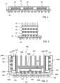
- Advanced packaging for integrated circuit dies may provide a configuration like that shown in Figure 1 where multiple integrated circuit dies 10 are mounted (in flip chip orientation) to the upper surface of a support substrate 12 (including a power/signal routing network 14) and share an overlying heatsink 16 thermally coupled to the dies and mounted to the substrate, or a configuration like that shown in Figure 2 wherein the multiple integrated circuit dies 10 are stacked one on top of the other (in flip chip orientation with through silicon vias (TSVs) in a thermally and electrically coupled relationship), supported by an underlying support substrate 12 (including a power/signal routing network 14) and capped with a heatsink 16 thermally coupled to an upper-most one of the dies.
- TSVs through silicon vias
- the packaging solution illustrated in Figure 1 suffers from the drawbacks associated with the side-by-side die configuration of necessitating longer interconnects between dies and having a package footprint which occupies an overly large area.
- the packaging solution illustrated in Figure 2 suffers from the drawbacks associated with the stacked die configuration of being overly complex, expensive and having constraints in heat dissipation.
- the packaging solution would provide both a reduced package footprint and improved heat dissipation in comparison to packaging solutions like that shown in Figures 1 and 2 .
- a package comprises: a support substrate including routing network; wherein the support substrate includes a center portion and at least one peripheral portion connected to the center portion by a flexible coupling region; a first circuit device having a front mounted to an upper surface of the support substrate at the center portion and electrically coupled to the routing network; a second circuit device having a front mounted to the upper surface of the support substrate at the at least one peripheral portion and electrically coupled to the routing network; a heatsink comprising a base plate, a plurality of fins extending from an upper surface of the base plate and a plurality of tabs extending from a lower surface of the base plate; wherein the tabs of the heatsink are mounted to the upper surface of the support substrate at the center portion, and the lower surface of the base plate is thermally coupled to a back of said first circuit device; wherein the at least one peripheral portion is folded relative to the center portion at the flexible coupling region; and wherein an outer surface of at least one fin of the heatsink is thermally coupled to a back of said
- a package comprises: a support substrate including routing network; wherein the support substrate includes a center portion and at least one peripheral portion connected to the center portion by a flexible coupling region; a first circuit device having a front mounted to an upper surface of the support substrate at the center portion and electrically coupled to the routing network; a second circuit device having a front mounted to the upper surface of the support substrate at the at least one peripheral portion and electrically coupled to the routing network; a heatsink comprising a base plate and a plurality of tabs extending from a lower surface of the base plate; wherein the tabs of the heatsink are mounted to the upper surface of the support substrate at the center portion, and the lower surface of the base plate is thermally coupled to a back of said first circuit device; wherein the at least one peripheral portion is folded relative to the center portion at the flexible coupling region; and wherein an outer surface of at least one tab of the heatsink is thermally coupled to a back of said second circuit device.
- FIG. 3 illustrates a package 100 for multiple integrated circuit dies 102.
- a flexible multi-layer support substrate 104 includes a power/signal routing network 106.
- the support substrate 104 includes a center portion 104C and at least one peripheral portion 104P.
- the peripheral portions 104P are foldable with respect to the center portion 104C at flexible fold areas 104F (comprising, for example, a flexible coupling region of the support substrate 104).
- the peripheral portions 104P are folded at a 90° angle with respect to the center portion 104C.
- the flexible multi-layer support substrate 104 may be rigid (or substantially rigid) at the peripheral portions 104P and the center portion 104C, while being flexible at the flexible fold areas 104F.
- Figure 4 illustrates an unfolded plan (top) view of the support substrate 104.
- the upper surface of the support substrate 104 includes, at each of the peripheral portions 104P and the center portion 104C, an array of interconnect pads 110. These interconnect pads are electrically connected to the power/signal routing network 106.
- the integrated circuit dies 102 are mounted to the upper surface of the support substrate 104 in flip chip orientation (i.e., with the front of the die facing the support substrate 104) as shown in Figure 5 .
- the interconnect balls 112 (or pillars) of the integrated circuit die 102 are soldered to the array of interconnect pads 110.
- a suitable adhesive fill may be provided to encapsulate the interconnect balls 112 and secure the integrated circuit die 102 to the support substrate 104.
- the center portion 104C of the support substrate 104 may have a quadrilateral (square or rectangular) shape, with each of the peripheral portions 104P also having a quadrilateral (square or rectangular) shape.
- Each peripheral portion 104P coupled by a flexible coupling region at the flexible fold area 104F, extends perpendicularly away from a side of the quadrilateral shape. While a quadrilateral shape for the center portion 104C of the support substrate 104 is a preferred embodiment, it will be understood that the center portion 104C may instead have some other geometric shape (such as a triangle shape, pentagon shape, or hexagon shape) determined, for example, by the number of integrated circuit dies 102 to be included in the package 10.
- the package 100 further includes a heat sink 120.
- the heat sink 120 includes a base plate 120B with a plurality of fins 120F extending from an upper surface of the base plate 120B.
- the heat sink 120 further includes a plurality of tabs 120T extending from a lower surface of the base plate 120B.
- the base plate 120B, fins 120F and tabs 120T form a unitary solid body (for example, made of aluminum or copper) that is manufactured as a single piece of material using suitable fabrication techniques such as milling, casting, extrusion or molding, for example.
- the lower surface of the base plate 120B is positioned in thermal contact with the back of the integrated circuit die 102 mounted to the center portion 104C of the support substrate 104.
- a layer of a thermally conductive adhesive 122 is used between the lower surface of the base plate 120B and the back of the integrated circuit die 102.
- the distal ends 121 of the tabs 120T are positioned in contact with the upper surface of the support substrate 104 at the center portion 104C.
- a suitable adhesive 124 for example an epoxy, is used to secure the tabs 120T of the heat sink 120 to the upper surface of the center portion 104C of the support substrate 104.
- peripheral portions 104P with the integrated circuit dies 102 mounted thereto, are then folded at the flexible fold areas 104F with a 90° angle with respect to the center portion 104C.
- a layer of a thermally conductive adhesive 126 is used to secure the back of each integrated circuit die 102 mounted to a peripheral portion 104P to the outer surface(s) of the fin(s) 120F of the heat sink 120.
- each tab 120T is aligned with a corresponding one of the fins 120F.
- the back of each integrated circuit die 102 mounted to the peripheral portion 104P is also secured by the layer of thermally conductive adhesive 126 to the outer surface(s) of the tab 120T of the heat sink 120. This serves to provide a larger heat dissipation area of the heatsink in thermal contact with the die 102.
- Figures 4-5 show an implementation for a package supporting five integrated circuit dies 102, it will be understood that this is by example only and that the package may instead be made with two, three or four integrated circuit dies 102 by adjusting the number of peripheral portions 104P that are included in the support substrate 104.
- the integrated circuit dies 102 are component parts of an electronic system where, for example, one of the dies may be a processor or controller integrated circuit, another one of the dies may be a memory integrated circuit, another one of the dies may be a communications integrated circuit, and another one of the dies may be a power management circuit.
- one or more of the dies may instead comprise a packaged circuit component.
- a packaged circuit component could be an active or passive component.
- the packaged circuit component could comprise a packaged integrated circuit, such as provided with a quad flat no-leads (QFN) type packaging or other surface mount packing configuration.
- QFN quad flat no-leads
- the bottom of the support substrate 104 at the center portion 104C includes a plurality of contact balls 140 (for example, in a ball grid array (BGA) format) that are electrically connected to the power/signal routing network 106.
- BGA ball grid array
- the package of Figure 3 has a number of advantages over the prior art: a) the package is compact with a small footprint; b) the heatsink is shared by all integrated circuit dies to provide for improved and efficient heat dissipation; c) the adhesive mounting of the tabs to the upper surface of the support substrate in connection with adhesively securing a surface of the heat sink to the back of each die provides for improved package rigidity and obviates the need for additional securing structures such as clamps, straps or caps.
Landscapes
- Cooling Or The Like Of Semiconductors Or Solid State Devices (AREA)
Abstract
A substrate includes a center portion and a peripheral portion connected to the center portion by a flexible coupling region. A first die is mounted to an upper surface of the substrate at the center portion and a second die is mounted to the upper surface of the substrate at the peripheral portion. A heatsink includes a base plate, fins extending from an upper surface of the base plate and tabs extending from a lower surface of the base plate. The tabs of the heatsink are mounted to the upper surface of the substrate at the center portion, and the lower surface of the base plate is thermally coupled to a back of the first die. The peripheral portion is folded relative to the center portion at the flexible coupling region. An outer surface of the fin of the heatsink is thermally coupled to a back of the second device.
Description
- This application claims priority from
United States Provisional Application for Patent No. 63/599,651, filed November 16, 2023 - The present invention relates to three-dimensional (3D) packages for multiple integrated circuit dies.
- Advanced packaging for integrated circuit dies may provide a configuration like that shown in
Figure 1 where multiple integrated circuit dies 10 are mounted (in flip chip orientation) to the upper surface of a support substrate 12 (including a power/signal routing network 14) and share anoverlying heatsink 16 thermally coupled to the dies and mounted to the substrate, or a configuration like that shown inFigure 2 wherein the multipleintegrated circuit dies 10 are stacked one on top of the other (in flip chip orientation with through silicon vias (TSVs) in a thermally and electrically coupled relationship), supported by an underlying support substrate 12 (including a power/signal routing network 14) and capped with aheatsink 16 thermally coupled to an upper-most one of the dies. - The packaging solution illustrated in
Figure 1 suffers from the drawbacks associated with the side-by-side die configuration of necessitating longer interconnects between dies and having a package footprint which occupies an overly large area. The packaging solution illustrated inFigure 2 suffers from the drawbacks associated with the stacked die configuration of being overly complex, expensive and having constraints in heat dissipation. - There is a need in the art for a better packaging solution for multiple integrated circuit dies. Preferably, the packaging solution would provide both a reduced package footprint and improved heat dissipation in comparison to packaging solutions like that shown in
Figures 1 and 2 . - In an embodiment, a package comprises: a support substrate including routing network; wherein the support substrate includes a center portion and at least one peripheral portion connected to the center portion by a flexible coupling region; a first circuit device having a front mounted to an upper surface of the support substrate at the center portion and electrically coupled to the routing network; a second circuit device having a front mounted to the upper surface of the support substrate at the at least one peripheral portion and electrically coupled to the routing network; a heatsink comprising a base plate, a plurality of fins extending from an upper surface of the base plate and a plurality of tabs extending from a lower surface of the base plate; wherein the tabs of the heatsink are mounted to the upper surface of the support substrate at the center portion, and the lower surface of the base plate is thermally coupled to a back of said first circuit device; wherein the at least one peripheral portion is folded relative to the center portion at the flexible coupling region; and wherein an outer surface of at least one fin of the heatsink is thermally coupled to a back of said second circuit device.
- In an embodiment, a package comprises: a support substrate including routing network; wherein the support substrate includes a center portion and at least one peripheral portion connected to the center portion by a flexible coupling region; a first circuit device having a front mounted to an upper surface of the support substrate at the center portion and electrically coupled to the routing network; a second circuit device having a front mounted to the upper surface of the support substrate at the at least one peripheral portion and electrically coupled to the routing network; a heatsink comprising a base plate and a plurality of tabs extending from a lower surface of the base plate; wherein the tabs of the heatsink are mounted to the upper surface of the support substrate at the center portion, and the lower surface of the base plate is thermally coupled to a back of said first circuit device; wherein the at least one peripheral portion is folded relative to the center portion at the flexible coupling region; and wherein an outer surface of at least one tab of the heatsink is thermally coupled to a back of said second circuit device.
- For the understanding of the present invention, embodiments thereof are now described, purely as a non-limitative example, with reference to the enclosed drawings, wherein:
-
Figure 1 illustrates a package for multiple integrated circuit dies; -
Figure 2 illustrates a package for multiple integrated circuit dies; -
Figure 3 illustrates a package for multiple integrated circuit dies; -
Figure 4 illustrates an unfolded plan (top) view of the support substrate used in the package ofFigure 3 ; and -
Figure 5 shows integrated circuit dies mounted to the support substrate. - The following description refers to the arrangement shown in the drawings; consequently, expressions such as "above", "below", "upper", "lower", "top", "bottom", "right", "left" and the like are relative to the attached Figures and should not be interpreted in a limiting way.
- The illustrations in the attached Figures are not necessary drawn to scale and certain features have been exaggerated in size, shape, extent, etc., in order to more clearly show the subject matter.
-
Figure 3 illustrates apackage 100 for multiple integrated circuit dies 102. A flexiblemulti-layer support substrate 104 includes a power/signal routing network 106. Thesupport substrate 104 includes acenter portion 104C and at least oneperipheral portion 104P. Theperipheral portions 104P are foldable with respect to thecenter portion 104C atflexible fold areas 104F (comprising, for example, a flexible coupling region of the support substrate 104). In a preferred, but not limiting, implementation, theperipheral portions 104P are folded at a 90° angle with respect to thecenter portion 104C. - In an embodiment, the flexible
multi-layer support substrate 104 may be rigid (or substantially rigid) at theperipheral portions 104P and thecenter portion 104C, while being flexible at theflexible fold areas 104F. -
Figure 4 illustrates an unfolded plan (top) view of thesupport substrate 104. The upper surface of thesupport substrate 104 includes, at each of theperipheral portions 104P and thecenter portion 104C, an array ofinterconnect pads 110. These interconnect pads are electrically connected to the power/signal routing network 106. Theintegrated circuit dies 102 are mounted to the upper surface of thesupport substrate 104 in flip chip orientation (i.e., with the front of the die facing the support substrate 104) as shown inFigure 5 . The interconnect balls 112 (or pillars) of theintegrated circuit die 102 are soldered to the array ofinterconnect pads 110. A suitable adhesive fill may be provided to encapsulate theinterconnect balls 112 and secure the integrated circuit die 102 to thesupport substrate 104. - In an embodiment, the
center portion 104C of thesupport substrate 104 may have a quadrilateral (square or rectangular) shape, with each of theperipheral portions 104P also having a quadrilateral (square or rectangular) shape. Eachperipheral portion 104P, coupled by a flexible coupling region at theflexible fold area 104F, extends perpendicularly away from a side of the quadrilateral shape. While a quadrilateral shape for thecenter portion 104C of thesupport substrate 104 is a preferred embodiment, it will be understood that thecenter portion 104C may instead have some other geometric shape (such as a triangle shape, pentagon shape, or hexagon shape) determined, for example, by the number of integrated circuit dies 102 to be included in thepackage 10. - With reference once again to
Figure 3 , thepackage 100 further includes aheat sink 120. Theheat sink 120 includes abase plate 120B with a plurality offins 120F extending from an upper surface of thebase plate 120B. Theheat sink 120 further includes a plurality oftabs 120T extending from a lower surface of thebase plate 120B. Thebase plate 120B,fins 120F andtabs 120T form a unitary solid body (for example, made of aluminum or copper) that is manufactured as a single piece of material using suitable fabrication techniques such as milling, casting, extrusion or molding, for example. - The lower surface of the
base plate 120B is positioned in thermal contact with the back of theintegrated circuit die 102 mounted to thecenter portion 104C of thesupport substrate 104. A layer of a thermallyconductive adhesive 122 is used between the lower surface of thebase plate 120B and the back of the integrated circuit die 102. Thedistal ends 121 of thetabs 120T are positioned in contact with the upper surface of thesupport substrate 104 at thecenter portion 104C. Asuitable adhesive 124, for example an epoxy, is used to secure thetabs 120T of theheat sink 120 to the upper surface of thecenter portion 104C of thesupport substrate 104. - The
peripheral portions 104P, with the integrated circuit dies 102 mounted thereto, are then folded at theflexible fold areas 104F with a 90° angle with respect to thecenter portion 104C. A layer of a thermallyconductive adhesive 126 is used to secure the back of eachintegrated circuit die 102 mounted to aperipheral portion 104P to the outer surface(s) of the fin(s) 120F of theheat sink 120. It will also be noted that eachtab 120T is aligned with a corresponding one of thefins 120F. With this configuration, the back of eachintegrated circuit die 102 mounted to theperipheral portion 104P is also secured by the layer of thermallyconductive adhesive 126 to the outer surface(s) of thetab 120T of theheat sink 120. This serves to provide a larger heat dissipation area of the heatsink in thermal contact with the die 102. - Although
Figures 4-5 show an implementation for a package supporting five integratedcircuit dies 102, it will be understood that this is by example only and that the package may instead be made with two, three or four integrated circuit dies 102 by adjusting the number ofperipheral portions 104P that are included in thesupport substrate 104. - In an implementation, the
integrated circuit dies 102 are component parts of an electronic system where, for example, one of the dies may be a processor or controller integrated circuit, another one of the dies may be a memory integrated circuit, another one of the dies may be a communications integrated circuit, and another one of the dies may be a power management circuit. - In an implementation, one or more of the dies may instead comprise a packaged circuit component. Such a circuit component could be an active or passive component. The packaged circuit component could comprise a packaged integrated circuit, such as provided with a quad flat no-leads (QFN) type packaging or other surface mount packing configuration.
- To permit the package to be electrically connected to other circuitry, and further to be mounted to a printed circuit board (PCB), the bottom of the
support substrate 104 at thecenter portion 104C includes a plurality of contact balls 140 (for example, in a ball grid array (BGA) format) that are electrically connected to the power/signal routing network 106. - The package of
Figure 3 has a number of advantages over the prior art: a) the package is compact with a small footprint; b) the heatsink is shared by all integrated circuit dies to provide for improved and efficient heat dissipation; c) the adhesive mounting of the tabs to the upper surface of the support substrate in connection with adhesively securing a surface of the heat sink to the back of each die provides for improved package rigidity and obviates the need for additional securing structures such as clamps, straps or caps. - While the invention has been illustrated and described in detail in the drawings and foregoing description, such illustration and description are considered illustrative or exemplary and not restrictive; the invention is not limited to the disclosed embodiments. Other variations to the disclosed embodiments can be understood and effected by those skilled in the art in practicing the claimed invention, from a study of the drawings, the disclosure, and the appended claims.
Claims (15)
- A package, comprising:a support substrate including routing network;wherein the support substrate includes a center portion and at least one peripheral portion connected to the center portion by a flexible coupling region;a first circuit device having a front mounted to an upper surface of the support substrate at the center portion and electrically coupled to the routing network;a second circuit device having a front mounted to the upper surface of the support substrate at the at least one peripheral portion and electrically coupled to the routing network;a heatsink comprising a base plate, a plurality of fins extending from an upper surface of the base plate and a plurality of tabs extending from a lower surface of the base plate;wherein the tabs of the heatsink are mounted to the upper surface of the support substrate at the center portion, and the lower surface of the base plate is thermally coupled to a back of said first circuit device;wherein the at least one peripheral portion is folded relative to the center portion at the flexible coupling region; andwherein an outer surface of at least one fin of the heatsink is thermally coupled to a back of said second circuit device.
- The package of claim 1, wherein each tab of the heatsink has a distal end positioned in contact with the upper surface of the support substrate at the center portion.
- The package of claim 2, further comprising an adhesive material securing the at least one tab of the heatsink to the upper surface of the support substrate at the center portion.
- The package of claim 1, wherein an outer surface of at least one tab of the heatsink is also thermally coupled to the back of said second circuit device.
- The package of claim 1, further comprising a ball grid array at a lower surface of the support substrate at the center portion, wherein said ball grid array is electrically coupled to the routing network.
- The package of claim 1, wherein the first and second circuit devices are integrated circuit dies mounted to the support substrate in flip chip orientation.
- The package of claim 1, wherein at least one of the first and second circuit devices is a packaged integrated circuit.
- The package of claim 7, wherein a package for the packaged integrated circuit is quad flat no-leads (QFN) package.
- A package, comprising:a support substrate including routing network;wherein the support substrate includes a center portion and at least one peripheral portion connected to the center portion by a flexible coupling region;a first circuit device having a front mounted to an upper surface of the support substrate at the center portion and electrically coupled to the routing network;a second circuit device having a front mounted to the upper surface of the support substrate at the at least one peripheral portion and electrically coupled to the routing network;a heatsink comprising a base plate and a plurality of tabs extending from a lower surface of the base plate;wherein the tabs of the heatsink are mounted to the upper surface of the support substrate at the center portion, and the lower surface of the base plate is thermally coupled to a back of said first circuit device;wherein the at least one peripheral portion is folded relative to the center portion at the flexible coupling region; andwherein an outer surface of at least one tab of the heatsink is thermally coupled to a back of said second circuit device.
- The package of claim 9, wherein each tab of the heatsink has a distal end positioned in contact with the upper surface of the support substrate at the center portion.
- The package of claim 10, further comprising an adhesive material securing the at least one tab of the heatsink to the upper surface of the support substrate at the center portion.
- The package of claim 9, further comprising a ball grid array at a lower surface of the support substrate at the center portion, wherein said ball grid array is electrically coupled to the routing network.
- The package of claim 9, wherein the first and second circuit devices are integrated circuit dies mounted to the support substrate in flip chip orientation.
- The package of claim 9, wherein at least one of the first and second circuit devices is a packaged integrated circuit.
- The package of claim 14, wherein a package for the packaged integrated circuit is quad flat no-leads (QFN) package.
Applications Claiming Priority (2)
| Application Number | Priority Date | Filing Date | Title |
|---|---|---|---|
| US202363599651P | 2023-11-16 | 2023-11-16 | |
| US18/907,998 US20250167067A1 (en) | 2023-11-16 | 2024-10-07 | Multidie flip chip package with heat sink |
Publications (1)
| Publication Number | Publication Date |
|---|---|
| EP4557366A1 true EP4557366A1 (en) | 2025-05-21 |
Family
ID=93520755
Family Applications (1)
| Application Number | Title | Priority Date | Filing Date |
|---|---|---|---|
| EP24212417.0A Pending EP4557366A1 (en) | 2023-11-16 | 2024-11-12 | Multidie flip chip package with heat sink |
Country Status (3)
| Country | Link |
|---|---|
| US (1) | US20250167067A1 (en) |
| EP (1) | EP4557366A1 (en) |
| CN (1) | CN120015714A (en) |
Citations (2)
| Publication number | Priority date | Publication date | Assignee | Title |
|---|---|---|---|---|
| US20040233641A1 (en) * | 2003-05-19 | 2004-11-25 | Mark Moshayedi | Processor/memory module with foldable substrate |
| US7082033B1 (en) * | 1998-02-13 | 2006-07-25 | Micron Technology, Inc. | Removing heat from integrated circuit devices mounted on a support structure |
-
2024
- 2024-10-07 US US18/907,998 patent/US20250167067A1/en active Pending
- 2024-10-30 CN CN202411524815.XA patent/CN120015714A/en active Pending
- 2024-11-12 EP EP24212417.0A patent/EP4557366A1/en active Pending
Patent Citations (2)
| Publication number | Priority date | Publication date | Assignee | Title |
|---|---|---|---|---|
| US7082033B1 (en) * | 1998-02-13 | 2006-07-25 | Micron Technology, Inc. | Removing heat from integrated circuit devices mounted on a support structure |
| US20040233641A1 (en) * | 2003-05-19 | 2004-11-25 | Mark Moshayedi | Processor/memory module with foldable substrate |
Also Published As
| Publication number | Publication date |
|---|---|
| US20250167067A1 (en) | 2025-05-22 |
| CN120015714A (en) | 2025-05-16 |
Similar Documents
| Publication | Publication Date | Title |
|---|---|---|
| US7250675B2 (en) | Method and apparatus for forming stacked die and substrate structures for increased packing density | |
| CN108573936B (en) | Semiconductor packaging | |
| JP4422323B2 (en) | Semiconductor device | |
| JP4746283B2 (en) | Method of connecting a heat sink to a circuit assembly and integrated circuit device | |
| US6265771B1 (en) | Dual chip with heat sink | |
| EP0729183A2 (en) | Thin packaging of multi-chip modules with enhanced thermal/power management | |
| US20020195697A1 (en) | Stacked mass storage flash memory package | |
| US20100213600A1 (en) | Apparatus having thermal-enhanced and cost-effective 3D IC integration structure with through silicon via interposers | |
| US8331094B2 (en) | Thermal and power bus stacked package architecture | |
| KR102170197B1 (en) | Package-on-package structures | |
| KR102854683B1 (en) | Semiconductor packages including heat dissipation layer | |
| US12616029B2 (en) | Package structure with stiffener ring having slant sidewall | |
| CN114765144A (en) | Semiconductor packaging structure | |
| TWI540653B (en) | Method and arrangement for semiconductor package including multi-memory die | |
| TWI832050B (en) | Semiconductor device and manufacturing method thereof | |
| US6973715B2 (en) | Method of forming a multichip module having chips on two sides | |
| TWI903759B (en) | Integrated circuit system and fabrication method thereof | |
| US20050230842A1 (en) | Multi-chip flip package with substrate for inter-die coupling | |
| US20250167067A1 (en) | Multidie flip chip package with heat sink | |
| US20250349629A1 (en) | Package structure and method for forming the same | |
| US8581385B2 (en) | Semiconductor chip to dissipate heat, semiconductor package including the same, and stack package using the same | |
| US20200227355A1 (en) | Through-Core Via | |
| CN221149994U (en) | Electronic devices and electronic components | |
| US9087702B2 (en) | Edge coupling of semiconductor dies | |
| US20240128195A1 (en) | Semiconductor package |
Legal Events
| Date | Code | Title | Description |
|---|---|---|---|
| PUAI | Public reference made under article 153(3) epc to a published international application that has entered the european phase |
Free format text: ORIGINAL CODE: 0009012 |
|
| STAA | Information on the status of an ep patent application or granted ep patent |
Free format text: STATUS: REQUEST FOR EXAMINATION WAS MADE |
|
| 17P | Request for examination filed |
Effective date: 20241112 |
|
| AK | Designated contracting states |
Kind code of ref document: A1 Designated state(s): AL AT BE BG CH CY CZ DE DK EE ES FI FR GB GR HR HU IE IS IT LI LT LU LV MC ME MK MT NL NO PL PT RO RS SE SI SK SM TR |