EP4557353A2 - Semiconductor device having integrated lid structure and method therefor - Google Patents
Semiconductor device having integrated lid structure and method therefor Download PDFInfo
- Publication number
- EP4557353A2 EP4557353A2 EP24213114.2A EP24213114A EP4557353A2 EP 4557353 A2 EP4557353 A2 EP 4557353A2 EP 24213114 A EP24213114 A EP 24213114A EP 4557353 A2 EP4557353 A2 EP 4557353A2
- Authority
- EP
- European Patent Office
- Prior art keywords
- lid structure
- encapsulant
- cavity
- semiconductor die
- semiconductor device
- Prior art date
- Legal status (The legal status is an assumption and is not a legal conclusion. Google has not performed a legal analysis and makes no representation as to the accuracy of the status listed.)
- Pending
Links
Images


Classifications
-
- H—ELECTRICITY
- H10—SEMICONDUCTOR DEVICES; ELECTRIC SOLID-STATE DEVICES NOT OTHERWISE PROVIDED FOR
- H10W—GENERIC PACKAGES, INTERCONNECTIONS, CONNECTORS OR OTHER CONSTRUCTIONAL DETAILS OF DEVICES COVERED BY CLASS H10
- H10W76/00—Containers; Fillings or auxiliary members therefor; Seals
- H10W76/10—Containers or parts thereof
- H10W76/12—Containers or parts thereof characterised by their shape
- H10W76/161—Containers comprising no base
-
- H—ELECTRICITY
- H10—SEMICONDUCTOR DEVICES; ELECTRIC SOLID-STATE DEVICES NOT OTHERWISE PROVIDED FOR
- H10W—GENERIC PACKAGES, INTERCONNECTIONS, CONNECTORS OR OTHER CONSTRUCTIONAL DETAILS OF DEVICES COVERED BY CLASS H10
- H10W76/00—Containers; Fillings or auxiliary members therefor; Seals
- H10W76/10—Containers or parts thereof
- H10W76/12—Containers or parts thereof characterised by their shape
-
- H—ELECTRICITY
- H10—SEMICONDUCTOR DEVICES; ELECTRIC SOLID-STATE DEVICES NOT OTHERWISE PROVIDED FOR
- H10W—GENERIC PACKAGES, INTERCONNECTIONS, CONNECTORS OR OTHER CONSTRUCTIONAL DETAILS OF DEVICES COVERED BY CLASS H10
- H10W40/00—Arrangements for thermal protection or thermal control
- H10W40/20—Arrangements for cooling
- H10W40/22—Arrangements for cooling characterised by their shape, e.g. having conical or cylindrical projections
-
- H—ELECTRICITY
- H10—SEMICONDUCTOR DEVICES; ELECTRIC SOLID-STATE DEVICES NOT OTHERWISE PROVIDED FOR
- H10W—GENERIC PACKAGES, INTERCONNECTIONS, CONNECTORS OR OTHER CONSTRUCTIONAL DETAILS OF DEVICES COVERED BY CLASS H10
- H10W40/00—Arrangements for thermal protection or thermal control
- H10W40/70—Fillings or auxiliary members in containers or in encapsulations for thermal protection or control
- H10W40/77—Auxiliary members characterised by their shape
- H10W40/778—Auxiliary members characterised by their shape in encapsulations
-
- H—ELECTRICITY
- H10—SEMICONDUCTOR DEVICES; ELECTRIC SOLID-STATE DEVICES NOT OTHERWISE PROVIDED FOR
- H10W—GENERIC PACKAGES, INTERCONNECTIONS, CONNECTORS OR OTHER CONSTRUCTIONAL DETAILS OF DEVICES COVERED BY CLASS H10
- H10W42/00—Arrangements for protection of devices
- H10W42/121—Arrangements for protection of devices protecting against mechanical damage
-
- H—ELECTRICITY
- H10—SEMICONDUCTOR DEVICES; ELECTRIC SOLID-STATE DEVICES NOT OTHERWISE PROVIDED FOR
- H10W—GENERIC PACKAGES, INTERCONNECTIONS, CONNECTORS OR OTHER CONSTRUCTIONAL DETAILS OF DEVICES COVERED BY CLASS H10
- H10W42/00—Arrangements for protection of devices
- H10W42/20—Arrangements for protection of devices protecting against electromagnetic or particle radiation, e.g. light, X-rays, gamma-rays or electrons
-
- H—ELECTRICITY
- H10—SEMICONDUCTOR DEVICES; ELECTRIC SOLID-STATE DEVICES NOT OTHERWISE PROVIDED FOR
- H10W—GENERIC PACKAGES, INTERCONNECTIONS, CONNECTORS OR OTHER CONSTRUCTIONAL DETAILS OF DEVICES COVERED BY CLASS H10
- H10W72/00—Interconnections or connectors in packages
- H10W72/071—Connecting or disconnecting
-
- H—ELECTRICITY
- H10—SEMICONDUCTOR DEVICES; ELECTRIC SOLID-STATE DEVICES NOT OTHERWISE PROVIDED FOR
- H10W—GENERIC PACKAGES, INTERCONNECTIONS, CONNECTORS OR OTHER CONSTRUCTIONAL DETAILS OF DEVICES COVERED BY CLASS H10
- H10W74/00—Encapsulations, e.g. protective coatings
- H10W74/01—Manufacture or treatment
-
- H—ELECTRICITY
- H10—SEMICONDUCTOR DEVICES; ELECTRIC SOLID-STATE DEVICES NOT OTHERWISE PROVIDED FOR
- H10W—GENERIC PACKAGES, INTERCONNECTIONS, CONNECTORS OR OTHER CONSTRUCTIONAL DETAILS OF DEVICES COVERED BY CLASS H10
- H10W76/00—Containers; Fillings or auxiliary members therefor; Seals
- H10W76/01—Manufacture or treatment
-
- H—ELECTRICITY
- H10—SEMICONDUCTOR DEVICES; ELECTRIC SOLID-STATE DEVICES NOT OTHERWISE PROVIDED FOR
- H10W—GENERIC PACKAGES, INTERCONNECTIONS, CONNECTORS OR OTHER CONSTRUCTIONAL DETAILS OF DEVICES COVERED BY CLASS H10
- H10W76/00—Containers; Fillings or auxiliary members therefor; Seals
- H10W76/60—Seals
-
- H—ELECTRICITY
- H10—SEMICONDUCTOR DEVICES; ELECTRIC SOLID-STATE DEVICES NOT OTHERWISE PROVIDED FOR
- H10W—GENERIC PACKAGES, INTERCONNECTIONS, CONNECTORS OR OTHER CONSTRUCTIONAL DETAILS OF DEVICES COVERED BY CLASS H10
- H10W72/00—Interconnections or connectors in packages
- H10W72/071—Connecting or disconnecting
- H10W72/073—Connecting or disconnecting of die-attach connectors
-
- H—ELECTRICITY
- H10—SEMICONDUCTOR DEVICES; ELECTRIC SOLID-STATE DEVICES NOT OTHERWISE PROVIDED FOR
- H10W—GENERIC PACKAGES, INTERCONNECTIONS, CONNECTORS OR OTHER CONSTRUCTIONAL DETAILS OF DEVICES COVERED BY CLASS H10
- H10W72/00—Interconnections or connectors in packages
- H10W72/20—Bump connectors, e.g. solder bumps or copper pillars; Dummy bumps; Thermal bumps
- H10W72/29—Bond pads specially adapted therefor
-
- H—ELECTRICITY
- H10—SEMICONDUCTOR DEVICES; ELECTRIC SOLID-STATE DEVICES NOT OTHERWISE PROVIDED FOR
- H10W—GENERIC PACKAGES, INTERCONNECTIONS, CONNECTORS OR OTHER CONSTRUCTIONAL DETAILS OF DEVICES COVERED BY CLASS H10
- H10W72/00—Interconnections or connectors in packages
- H10W72/30—Die-attach connectors
- H10W72/331—Shapes of die-attach connectors
- H10W72/332—Plan-view shape, i.e. in top view
-
- H—ELECTRICITY
- H10—SEMICONDUCTOR DEVICES; ELECTRIC SOLID-STATE DEVICES NOT OTHERWISE PROVIDED FOR
- H10W—GENERIC PACKAGES, INTERCONNECTIONS, CONNECTORS OR OTHER CONSTRUCTIONAL DETAILS OF DEVICES COVERED BY CLASS H10
- H10W72/00—Interconnections or connectors in packages
- H10W72/851—Dispositions of multiple connectors or interconnections
- H10W72/874—On different surfaces
- H10W72/877—Bump connectors and die-attach connectors
-
- H—ELECTRICITY
- H10—SEMICONDUCTOR DEVICES; ELECTRIC SOLID-STATE DEVICES NOT OTHERWISE PROVIDED FOR
- H10W—GENERIC PACKAGES, INTERCONNECTIONS, CONNECTORS OR OTHER CONSTRUCTIONAL DETAILS OF DEVICES COVERED BY CLASS H10
- H10W90/00—Package configurations
- H10W90/701—Package configurations characterised by the relative positions of pads or connectors relative to package parts
- H10W90/721—Package configurations characterised by the relative positions of pads or connectors relative to package parts of bump connectors
- H10W90/724—Package configurations characterised by the relative positions of pads or connectors relative to package parts of bump connectors between a chip and a stacked insulating package substrate, interposer or RDL
-
- H—ELECTRICITY
- H10—SEMICONDUCTOR DEVICES; ELECTRIC SOLID-STATE DEVICES NOT OTHERWISE PROVIDED FOR
- H10W—GENERIC PACKAGES, INTERCONNECTIONS, CONNECTORS OR OTHER CONSTRUCTIONAL DETAILS OF DEVICES COVERED BY CLASS H10
- H10W90/00—Package configurations
- H10W90/701—Package configurations characterised by the relative positions of pads or connectors relative to package parts
- H10W90/731—Package configurations characterised by the relative positions of pads or connectors relative to package parts of die-attach connectors
- H10W90/736—Package configurations characterised by the relative positions of pads or connectors relative to package parts of die-attach connectors between a chip and a stacked lead frame, conducting package substrate or heat sink
Definitions
- This disclosure relates generally to semiconductor device packaging, and more specifically, to a semiconductor device having an integrated lid structure and method of forming the same.
- a semiconductor device having an integrated lid structure.
- the semiconductor device includes a semiconductor die mounted in a cavity of the lid structure such that sidewalls of the lid substantially surround sidewalls of the semiconductor die.
- a backside of the semiconductor die is affixed to the bottom of the cavity by way of a thermally conductive adhesive.
- the mounted semiconductor die and lid structure are at least partially encapsulated with an encapsulant.
- a first portion of the encapsulant the surrounds an outer perimeter of the lid structure and a second portion of the encapsulant substantially fills a gap region of the cavity between the semiconductor die and sidewalls of the cavity. After encapsulation, top and bottom surfaces of the lid structure are exposed, and an active side of the semiconductor die is exposed.
- a plurality of conductive connectors 616 are affixed to respective the die pads 404.
- the conductive connectors 616 are configured and arranged to provide conductive connections between the semiconductor device 100 and a printed circuit board (PCB), for example.
- a plurality of conductive connectors (e.g., solder balls) are affixed to respective die pads of the semiconductor die.
- the conductive connectors are configured and arranged to provide conductive connections between the semiconductor device and a printed circuit board, for example.
- the semiconductor device may be characterized as a high-performance or high-power flip-chip ball grid array (HFCBGA) type device. By forming the semiconductor device in this manner, the integrated lid structure provides enhanced thermal dissipation, electromagnetic interference (EMI) shielding, and warpage control.
- EMI electromagnetic interference
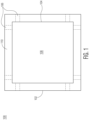
- FIG. 1 illustrates, in a simplified bottom-side-up plan view, an example semiconductor device 100 having an integrated lid structure at a stage of manufacture in accordance with an embodiment.
- the semiconductor device 100 includes a lid structure 102.
- a cavity 104 is formed in the lid structure 102.
- the cavity includes a bottom surface 108 surrounded by sidewalls of the lid structure 102.
- a plurality of grooves e.g., channels
- 106 are formed at the bottom surface 110 of the sidewall portions of the lid structure 102.
- the grooves 106 are configured to allow an encapsulant material (e.g., epoxy mold compound) to flow into and through the cavity 104 as desired during an encapsulation operation at a subsequent stage of manufacture, for example.
- the lid structure is formed from a metal material such as copper, aluminum, and the like.
- the metal material and thickness of the lid structure 102 may be chosen for desired thermal dissipation, electromagnetic interference (EMI) shielding, and warpage control characteristics, for example.
- EMI electromagnetic interference
- the size and shape of the lid structure 102 and corresponding cavity 104 along with the number and locations of the grooves 106 depicted in FIG. 1 are chosen for illustration purposes.
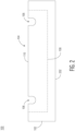
- FIG. 2 illustrates, in a simplified bottom-side-up side view, the example semiconductor device 100 having an integrated lid structure at the stage of manufacture depicted in FIG. 1 in accordance with an embodiment.
- a side portion of the lid structure 102 is illustrated in FIG. 2 .
- the cavity 104 of the lid structure 102 including the bottom surface 108 of the cavity are shown as dashed lines for reference.
- the plurality of grooves 106 are located at the bottom surface 110 of the sidewall portions of the lid structure 102.
- the lid structure 102 is arranged in a bottom side up orientation with the top surface 202 of the lid structure 102 located at the bottom of the illustration.
- FIG. 3 illustrates, in a simplified bottom-side-up plan view, the example semiconductor device 100 having an integrated lid structure at a subsequent stage of manufacture in accordance with an embodiment.
- the semiconductor device 100 includes a thermally conductive adhesive 302 applied on the bottom surface 108 of the cavity 104.
- Thermally conductive adhesive 302 may be applied as a tape or film or otherwise dispensed onto the bottom surface 108 of the cavity 104.
- the thermally conductive adhesive 302 is chosen for consistent, uniform, and accurate bondline thickness (BLT) characteristics when bonding a semiconductor die at a subsequent stage of manufacture, for example.
- BLT bondline thickness
- FIG. 4 illustrates, in a simplified bottom-side-up plan view, the example semiconductor device 100 having an integrated lid structure at a subsequent stage of manufacture in accordance with an embodiment.
- the semiconductor device 100 includes a semiconductor die 402 mounted within the cavity 104 of the lid structure 102.
- the semiconductor die 402 is affixed to the bottom surface 108 of the cavity 104 by way of the thermally conductive adhesive 302 applied on the bottom surface.
- desired consistent, uniform, and accurate BLT can be realized. These desired BLT characteristics may be critical to the reliability of high performance and high power devices, for example.
- the semiconductor die 402 has an active side (e.g., major side having circuitry, die pads) and a backside (e.g., major side opposite of the active side).
- the backside of the semiconductor die 402 is mounted the bottom surface 108 of the cavity 104 while die pads 404 at the active side of the semiconductor die 402 are exposed, for example.
- the semiconductor die 402 is configured in a flip-chip orientation having the die pads 404 at the active side arranged for attachment of conductive connectors (e.g., solder balls) at a subsequent stage of manufacture.
- the active side of the semiconductor die 402 is substantially coplanar with the bottom surface 110 of the sidewall portions of the lid structure 102.
- the semiconductor die 402 may be formed from any suitable semiconductor material, such as silicon, germanium, gallium arsenide, gallium nitride, and the like.
- the semiconductor die 402 may further include any digital circuits, analog circuits, RF circuits, power circuits, memory, processor, MEMs, sensor, the like, and combinations thereof at the active side.
- FIG. 5 illustrates, in a simplified bottom-side-up plan view, the example semiconductor device 100 having an integrated lid structure at a subsequent stage of manufacture in accordance with an embodiment.
- the semiconductor device 100 includes the semiconductor die 402 and the lid structure 102 at least partially encapsulated with an encapsulant 502 (e.g., epoxy molding compound).
- an encapsulant 502 e.g., epoxy molding compound
- the semiconductor die 402 and the lid structure 102 are molded with the encapsulant 502 by way of a molding process.
- the encapsulant 502 may be an epoxy molding compound dispensed during an injection molding encapsulation operation, for example.
- the semiconductor die 402 and the lid structure 102 may be molded with the encapsulant 502 by way of a film-assisted molding (FAM) process.
- FAM film-assisted molding
- a FAM tool using a conformal film may be engaged with predetermined portions of the semiconductor die 402 and the lid structure 102 during the molding process to keep the predetermined portions exposed and free from encapsulant.
- the encapsulant 502 surrounds an outer perimeter of the lid structure and substantially fills a gap region of the cavity between the semiconductor die 402 and sidewalls of the cavity.
- a portion 504 of the encapsulant fills the grooves 106 of FIG. 4 formed at the bottom surface 110 of the sidewall portions of the lid structure 102.
- the bottom surface 110 of the sidewall portions of the lid structure 102 and the active side of the semiconductor die 402 including the die pads 404 are exposed through the encapsulant 502 after the molding process.
- Cross-sectional views of the example semiconductor device 100 taken along line A-A of FIG. 5 at stages of manufacture are depicted in FIG. 6 and FIG. 7 .
- FIG. 6 illustrates, in a simplified top-side-up cross-sectional view, the example semiconductor device 100 having an integrated lid structure at the stage of manufacture depicted in FIG. 5 in accordance with an embodiment.
- the semiconductor device 100 includes the semiconductor die 402 and the lid structure 102 at least partially encapsulated with the encapsulant 502.
- the encapsulant 502 surrounds an outer sidewall surface 608 of the lid structure and substantially fills a gap region 608 of the cavity between sidewalls 602 of the semiconductor die 402 and inner sidewall surfaces 604 of the cavity 104.
- the bottom surface 110 of the sidewall portions of the lid structure 102 and the active side of the semiconductor die 402 including the die pads 404 are exposed through the encapsulant 502 at the bottom side of the semiconductor device 100 after the molding process.
- the top surface 202 of the lid structure 102 is exposed through the encapsulant 502 at the top side of the semiconductor device 100 after the molding process.
- a plurality of conductive connectors 616 e.g., solder balls
- the conductive connectors 616 are configured and arranged to provide conductive connections between the semiconductor device 100 and a printed circuit board (PCB), for example.
- the conductive connectors 616 may be in the form of any suitable conductive structures such as solder balls, gold studs, copper pillars, and the like, to connect conductive features of the semiconductor device 100 with the PCB.
- the die pads 404 may be subsequent connected to the PCB by way of solder paste attachment or other suitable conductive attachment processes (e.g., ACF, ACP).
- a top surface 610 of the encapsulant 502 surrounding the outer sidewall surface 608 of the lid structure 102 is substantially coplanar with the top surface 202 of the lid structure
- a bottom surface 612 of the encapsulant 502 surrounding the outer sidewall surface 608 of the lid structure 102 is substantially coplanar with the bottom surface 110 of the lid structure.
- the bottom surface 612 of the encapsulant 502 surrounding the outer sidewall surface 608 of the lid structure 102 is substantially coplanar with the bottom surface 614 of the encapsulant 502 filling the gap region 608 of the cavity between sidewalls 602 of the semiconductor die 402 and the inner sidewall surfaces 604 of the cavity 104.
- the active side of the semiconductor die 402 is substantially coplanar with the bottom surface 110 of the lid structure 102.
- FIG. 7 illustrates, in a simplified top-side-up cross-sectional view, the example semiconductor device 100 having an integrated lid structure at subsequent stage of manufacture in accordance with an embodiment.
- the semiconductor device 100 includes the encapsulated semiconductor die 402 and the lid structure 102 mounted on an example printed circuit board (PCB) 706.
- the plurality of conductive connectors 616 are affixed to respective connector pads 704 and configured to provide conductive connections between the die pads 404 and respective connector pads 704 of the PCB 706.
- the bottom surface 110 of the lid structure 102 is affixed to respective connector pads 704 by way of a conductive material 702 such as a solder paste or conductive adhesive material.
- the conductive connectors 616 are formed as ball connectors and arranged in a ball grid array.
- the term "conductive,” as used herein, generally refers to electrical conductivity unless otherwise described.
- a method including mounting a semiconductor die within a cavity of a lid structure, an active side of the semiconductor die substantially coplanar with a bottom surface of the lid structure; and encapsulating with an encapsulant to substantially fill a gap region between sidewalls of the semiconductor die and inner sidewall surfaces of the cavity.
- a top surface of the lid structure and the bottom surface of the lid structure may be exposed after encapsulating with the encapsulant.
- the encapsulating with the encapsulant may further include an outer region of the encapsulant surrounding outer sidewall surfaces of the lid structure.
- a bottom surface of the outer region of the encapsulant may be substantially coplanar with a bottom surface of the encapsulant in the gap region.
- a top surface of the outer region of the encapsulant may be substantially coplanar with a top surface of the lid structure.
- the method may further include dispensing a thermally conductive adhesive on a bottom surface of the cavity of the lid structure before mounting the semiconductor die.
- the mounting the semiconductor die within the cavity may include affixing a backside of the semiconductor die to the bottom surface of the cavity by way of the thermally conductive adhesive.
- the lid structure may be formed from a metal material, a plurality of grooves formed at the bottom surface of the lid structure. The plurality of grooves formed at the bottom surface of the lid structure may be configured to allow encapsulant to flow into the cavity.
- a semiconductor device including a lid structure having a top surface and outer sidewall surfaces; a cavity formed in the lid structure, the cavity having a bottom surface and inner sidewall surfaces; a semiconductor die mounted within the cavity such that the inner sidewall surfaces of the cavity surround the semiconductor die; and an encapsulant substantially filling a gap region between sidewalls of the semiconductor die and the inner sidewall surfaces of the cavity.
- An active side of the semiconductor die may be substantially coplanar with a bottom surface of the lid structure.
- a top surface of the lid structure and the bottom surface of the lid structure may be exposed through the encapsulant.
- the encapsulant may include an outer region encapsulating outer sidewall surfaces of the lid structure.
- a bottom surface of the outer region of the encapsulant may be substantially coplanar with a bottom surface of the encapsulant in the gap region.
- the lid structure may include a plurality of grooves formed at the bottom surface of the lid structure, the plurality of grooves configured to allow encapsulant to flow into the cavity during an encapsulation operation.
- a method including providing a lid structure having a top surface and outer sidewall surfaces, the lid structure including a cavity having a bottom surface and inner sidewall surfaces; mounting a semiconductor die within the cavity such that the inner sidewall surfaces of the cavity surround the semiconductor die; and encapsulating with an encapsulant to substantially fill a gap region between sidewalls of the semiconductor die and the inner sidewalls of the cavity.
- An active side of the semiconductor die may be substantially coplanar with a bottom surface of the lid structure after mounting the semiconductor die.
- a top surface of the lid structure and the bottom surface of the lid structure may be exposed after encapsulating with the encapsulant.
- the encapsulating with the encapsulant may further include an outer region of the encapsulant surrounding outer sidewall surfaces of the lid structure.
- the lid structure may include a plurality of grooves formed at the bottom surface of the lid structure, the plurality of grooves configured to allow encapsulant to flow into the cavity.
- the semiconductor device includes a semiconductor die mounted in a cavity of the lid structure such that sidewalls of the lid substantially surround sidewalls of the semiconductor die.
- a backside of the semiconductor die is affixed to the bottom of the cavity by way of a thermally conductive adhesive.
- the mounted semiconductor die and lid structure are at least partially encapsulated with an encapsulant.
- a first portion of the encapsulant the surrounds an outer perimeter of the lid structure and a second portion of the encapsulant substantially fills a gap region of the cavity between the semiconductor die and sidewalls of the cavity.
- top and bottom surfaces of the lid structure are exposed, and an active side of the semiconductor die is exposed.
- a plurality of conductive connectors 616 are affixed to respective the die pads 404.
- the conductive connectors 616 are configured and arranged to provide conductive connections between the semiconductor device 100 and a printed circuit board (PCB), for example.
- a plurality of conductive connectors (e.g., solder balls) are affixed to respective die pads of the semiconductor die.
- the conductive connectors are configured and arranged to provide conductive connections between the semiconductor device and a printed circuit board, for example.
- the semiconductor device may be characterized as a high-performance or high-power flip-chip ball grid array type device. By forming the semiconductor device in this manner, the integrated lid structure provides enhanced thermal dissipation, electromagnetic interference shielding, and warpage control.
Landscapes
- Structures Or Materials For Encapsulating Or Coating Semiconductor Devices Or Solid State Devices (AREA)
- Lead Frames For Integrated Circuits (AREA)
- Physics & Mathematics (AREA)
- Health & Medical Sciences (AREA)
- Electromagnetism (AREA)
- Toxicology (AREA)
Abstract
Description
- This disclosure relates generally to semiconductor device packaging, and more specifically, to a semiconductor device having an integrated lid structure and method of forming the same.
- Today, there is an increasing trend to include sophisticated semiconductor devices in products and systems that are used every day. These sophisticated semiconductor devices may include features for specific applications which may impact the configuration of the semiconductor device packages, for example. With such features and applications, the configuration of the semiconductor device packages may limit performance of the semiconductor devices or impact the costs of the semiconductor devices. Accordingly, significant challenges exist in accommodating these features and applications while minimizing the impact on semiconductor devices' performance and costs.
- The present invention is illustrated by way of example and is not limited by the accompanying figures, in which like references indicate similar elements. Elements in the figures are illustrated for simplicity and clarity and have not necessarily been drawn to scale.
-
FIG. 1 illustrates, in a simplified bottom-side-up plan view, an example semiconductor device having an integrated lid structure at a stage of manufacture in accordance with an embodiment. -
FIG. 2 illustrates, in a simplified side view, the example semiconductor device at the stage of manufacture depicted inFIG. 1 in accordance with an embodiment. -
FIG. 3 through FIG. 5 illustrate, in simplified bottom-side-up plan views, the example semiconductor device at subsequent stages of manufacture in accordance with an embodiment. -
FIG. 6 illustrates, in a simplified cross-sectional view, the example semiconductor device at the stage of manufacture depicted inFIG. 5 taken along line A-A in accordance with an embodiment. -
FIG. 7 illustrates, in a simplified cross-sectional view, the example semiconductor device taken along line A-A ofFIG. 5 at a subsequent stage of manufacture in accordance with an embodiment. - Generally, there is provided, a semiconductor device having an integrated lid structure. The semiconductor device includes a semiconductor die mounted in a cavity of the lid structure such that sidewalls of the lid substantially surround sidewalls of the semiconductor die. A backside of the semiconductor die is affixed to the bottom of the cavity by way of a thermally conductive adhesive. The mounted semiconductor die and lid structure are at least partially encapsulated with an encapsulant. A first portion of the encapsulant the surrounds an outer perimeter of the lid structure and a second portion of the encapsulant substantially fills a gap region of the cavity between the semiconductor die and sidewalls of the cavity. After encapsulation, top and bottom surfaces of the lid structure are exposed, and an active side of the semiconductor die is exposed. A plurality of conductive connectors 616 (e.g., solder balls) are affixed to respective the
die pads 404. Theconductive connectors 616 are configured and arranged to provide conductive connections between thesemiconductor device 100 and a printed circuit board (PCB), for example. A plurality of conductive connectors (e.g., solder balls) are affixed to respective die pads of the semiconductor die. The conductive connectors are configured and arranged to provide conductive connections between the semiconductor device and a printed circuit board, for example. The semiconductor device may be characterized as a high-performance or high-power flip-chip ball grid array (HFCBGA) type device. By forming the semiconductor device in this manner, the integrated lid structure provides enhanced thermal dissipation, electromagnetic interference (EMI) shielding, and warpage control. -
FIG. 1 illustrates, in a simplified bottom-side-up plan view, anexample semiconductor device 100 having an integrated lid structure at a stage of manufacture in accordance with an embodiment. At this stage, thesemiconductor device 100 includes alid structure 102. Acavity 104 is formed in thelid structure 102. The cavity includes abottom surface 108 surrounded by sidewalls of thelid structure 102. In this embodiment, a plurality of grooves (e.g., channels) 106 (indicated by dashed lines) are formed at thebottom surface 110 of the sidewall portions of thelid structure 102. Thegrooves 106 are configured to allow an encapsulant material (e.g., epoxy mold compound) to flow into and through thecavity 104 as desired during an encapsulation operation at a subsequent stage of manufacture, for example. In this embodiment, the lid structure is formed from a metal material such as copper, aluminum, and the like. The metal material and thickness of thelid structure 102 may be chosen for desired thermal dissipation, electromagnetic interference (EMI) shielding, and warpage control characteristics, for example. The size and shape of thelid structure 102 andcorresponding cavity 104 along with the number and locations of thegrooves 106 depicted inFIG. 1 are chosen for illustration purposes. -
FIG. 2 illustrates, in a simplified bottom-side-up side view, theexample semiconductor device 100 having an integrated lid structure at the stage of manufacture depicted inFIG. 1 in accordance with an embodiment. A side portion of thelid structure 102 is illustrated inFIG. 2 . Thecavity 104 of thelid structure 102 including thebottom surface 108 of the cavity are shown as dashed lines for reference. In this embodiment, the plurality ofgrooves 106 are located at thebottom surface 110 of the sidewall portions of thelid structure 102. As depicted inFIG. 2 , thelid structure 102 is arranged in a bottom side up orientation with thetop surface 202 of thelid structure 102 located at the bottom of the illustration. -
FIG. 3 illustrates, in a simplified bottom-side-up plan view, theexample semiconductor device 100 having an integrated lid structure at a subsequent stage of manufacture in accordance with an embodiment. At this stage, thesemiconductor device 100 includes a thermallyconductive adhesive 302 applied on thebottom surface 108 of thecavity 104. Thermallyconductive adhesive 302 may be applied as a tape or film or otherwise dispensed onto thebottom surface 108 of thecavity 104. In this embodiment, the thermallyconductive adhesive 302 is chosen for consistent, uniform, and accurate bondline thickness (BLT) characteristics when bonding a semiconductor die at a subsequent stage of manufacture, for example. -
FIG. 4 illustrates, in a simplified bottom-side-up plan view, theexample semiconductor device 100 having an integrated lid structure at a subsequent stage of manufacture in accordance with an embodiment. At this stage, thesemiconductor device 100 includes asemiconductor die 402 mounted within thecavity 104 of thelid structure 102. In this embodiment, thesemiconductor die 402 is affixed to thebottom surface 108 of thecavity 104 by way of the thermallyconductive adhesive 302 applied on the bottom surface. By utilizing the thermallyconductive adhesive 302 for mounting thesemiconductor die 402 in this manner, desired consistent, uniform, and accurate BLT can be realized. These desired BLT characteristics may be critical to the reliability of high performance and high power devices, for example. - The semiconductor die 402 has an active side (e.g., major side having circuitry, die pads) and a backside (e.g., major side opposite of the active side). In this embodiment, the backside of the
semiconductor die 402 is mounted thebottom surface 108 of thecavity 104 while diepads 404 at the active side of thesemiconductor die 402 are exposed, for example. In this embodiment, the semiconductor die 402 is configured in a flip-chip orientation having thedie pads 404 at the active side arranged for attachment of conductive connectors (e.g., solder balls) at a subsequent stage of manufacture. In this embodiment, the active side of thesemiconductor die 402 is substantially coplanar with thebottom surface 110 of the sidewall portions of thelid structure 102. The semiconductor die 402 may be formed from any suitable semiconductor material, such as silicon, germanium, gallium arsenide, gallium nitride, and the like. The semiconductor die 402 may further include any digital circuits, analog circuits, RF circuits, power circuits, memory, processor, MEMs, sensor, the like, and combinations thereof at the active side. -
FIG. 5 illustrates, in a simplified bottom-side-up plan view, theexample semiconductor device 100 having an integrated lid structure at a subsequent stage of manufacture in accordance with an embodiment. At this stage, thesemiconductor device 100 includes thesemiconductor die 402 and thelid structure 102 at least partially encapsulated with an encapsulant 502 (e.g., epoxy molding compound). In this embodiment, thesemiconductor die 402 and thelid structure 102 are molded with theencapsulant 502 by way of a molding process. Theencapsulant 502 may be an epoxy molding compound dispensed during an injection molding encapsulation operation, for example. Alternatively, the semiconductor die 402 and thelid structure 102 may be molded with theencapsulant 502 by way of a film-assisted molding (FAM) process. For example, a FAM tool using a conformal film may be engaged with predetermined portions of the semiconductor die 402 and thelid structure 102 during the molding process to keep the predetermined portions exposed and free from encapsulant. - In this embodiment, the
encapsulant 502 surrounds an outer perimeter of the lid structure and substantially fills a gap region of the cavity between the semiconductor die 402 and sidewalls of the cavity. Aportion 504 of the encapsulant fills thegrooves 106 ofFIG. 4 formed at thebottom surface 110 of the sidewall portions of thelid structure 102. In this embodiment, thebottom surface 110 of the sidewall portions of thelid structure 102 and the active side of the semiconductor die 402 including thedie pads 404 are exposed through theencapsulant 502 after the molding process. Cross-sectional views of theexample semiconductor device 100 taken along line A-A ofFIG. 5 at stages of manufacture are depicted inFIG. 6 andFIG. 7 . -
FIG. 6 illustrates, in a simplified top-side-up cross-sectional view, theexample semiconductor device 100 having an integrated lid structure at the stage of manufacture depicted inFIG. 5 in accordance with an embodiment. At this stage, thesemiconductor device 100 includes the semiconductor die 402 and thelid structure 102 at least partially encapsulated with theencapsulant 502. In this embodiment, theencapsulant 502 surrounds anouter sidewall surface 608 of the lid structure and substantially fills agap region 608 of the cavity betweensidewalls 602 of the semiconductor die 402 and inner sidewall surfaces 604 of thecavity 104. In this embodiment, thebottom surface 110 of the sidewall portions of thelid structure 102 and the active side of the semiconductor die 402 including thedie pads 404 are exposed through theencapsulant 502 at the bottom side of thesemiconductor device 100 after the molding process. Likewise, thetop surface 202 of thelid structure 102 is exposed through theencapsulant 502 at the top side of thesemiconductor device 100 after the molding process. A plurality of conductive connectors 616 (e.g., solder balls) are affixed to respective thedie pads 404. Theconductive connectors 616 are configured and arranged to provide conductive connections between thesemiconductor device 100 and a printed circuit board (PCB), for example. Theconductive connectors 616 may be in the form of any suitable conductive structures such as solder balls, gold studs, copper pillars, and the like, to connect conductive features of thesemiconductor device 100 with the PCB. As an alternative to attachingconductive connectors 616, thedie pads 404 may be subsequent connected to the PCB by way of solder paste attachment or other suitable conductive attachment processes (e.g., ACF, ACP). - In this embodiment, a
top surface 610 of theencapsulant 502 surrounding theouter sidewall surface 608 of thelid structure 102 is substantially coplanar with thetop surface 202 of the lid structure, and abottom surface 612 of theencapsulant 502 surrounding theouter sidewall surface 608 of thelid structure 102 is substantially coplanar with thebottom surface 110 of the lid structure. Likewise, thebottom surface 612 of theencapsulant 502 surrounding theouter sidewall surface 608 of thelid structure 102 is substantially coplanar with thebottom surface 614 of theencapsulant 502 filling thegap region 608 of the cavity betweensidewalls 602 of the semiconductor die 402 and the inner sidewall surfaces 604 of thecavity 104. And likewise, the active side of the semiconductor die 402 is substantially coplanar with thebottom surface 110 of thelid structure 102. -
FIG. 7 illustrates, in a simplified top-side-up cross-sectional view, theexample semiconductor device 100 having an integrated lid structure at subsequent stage of manufacture in accordance with an embodiment. At this stage, thesemiconductor device 100 includes the encapsulated semiconductor die 402 and thelid structure 102 mounted on an example printed circuit board (PCB) 706. In this embodiment, the plurality ofconductive connectors 616 are affixed torespective connector pads 704 and configured to provide conductive connections between thedie pads 404 andrespective connector pads 704 of thePCB 706. Likewise, thebottom surface 110 of thelid structure 102 is affixed torespective connector pads 704 by way of aconductive material 702 such as a solder paste or conductive adhesive material. For illustration purposes, theconductive connectors 616 are formed as ball connectors and arranged in a ball grid array. The term "conductive," as used herein, generally refers to electrical conductivity unless otherwise described. - Generally, there is provided, a method including mounting a semiconductor die within a cavity of a lid structure, an active side of the semiconductor die substantially coplanar with a bottom surface of the lid structure; and encapsulating with an encapsulant to substantially fill a gap region between sidewalls of the semiconductor die and inner sidewall surfaces of the cavity. A top surface of the lid structure and the bottom surface of the lid structure may be exposed after encapsulating with the encapsulant. The encapsulating with the encapsulant may further include an outer region of the encapsulant surrounding outer sidewall surfaces of the lid structure. A bottom surface of the outer region of the encapsulant may be substantially coplanar with a bottom surface of the encapsulant in the gap region. A top surface of the outer region of the encapsulant may be substantially coplanar with a top surface of the lid structure. The method may further include dispensing a thermally conductive adhesive on a bottom surface of the cavity of the lid structure before mounting the semiconductor die. The mounting the semiconductor die within the cavity may include affixing a backside of the semiconductor die to the bottom surface of the cavity by way of the thermally conductive adhesive. The lid structure may be formed from a metal material, a plurality of grooves formed at the bottom surface of the lid structure. The plurality of grooves formed at the bottom surface of the lid structure may be configured to allow encapsulant to flow into the cavity.
- In another embodiment, there is provided, a semiconductor device including a lid structure having a top surface and outer sidewall surfaces; a cavity formed in the lid structure, the cavity having a bottom surface and inner sidewall surfaces; a semiconductor die mounted within the cavity such that the inner sidewall surfaces of the cavity surround the semiconductor die; and an encapsulant substantially filling a gap region between sidewalls of the semiconductor die and the inner sidewall surfaces of the cavity. An active side of the semiconductor die may be substantially coplanar with a bottom surface of the lid structure. A top surface of the lid structure and the bottom surface of the lid structure may be exposed through the encapsulant. The encapsulant may include an outer region encapsulating outer sidewall surfaces of the lid structure. A bottom surface of the outer region of the encapsulant may be substantially coplanar with a bottom surface of the encapsulant in the gap region. The lid structure may include a plurality of grooves formed at the bottom surface of the lid structure, the plurality of grooves configured to allow encapsulant to flow into the cavity during an encapsulation operation.
- In yet another embodiment, there is provided, a method including providing a lid structure having a top surface and outer sidewall surfaces, the lid structure including a cavity having a bottom surface and inner sidewall surfaces; mounting a semiconductor die within the cavity such that the inner sidewall surfaces of the cavity surround the semiconductor die; and encapsulating with an encapsulant to substantially fill a gap region between sidewalls of the semiconductor die and the inner sidewalls of the cavity. An active side of the semiconductor die may be substantially coplanar with a bottom surface of the lid structure after mounting the semiconductor die. A top surface of the lid structure and the bottom surface of the lid structure may be exposed after encapsulating with the encapsulant. The encapsulating with the encapsulant may further include an outer region of the encapsulant surrounding outer sidewall surfaces of the lid structure. The lid structure may include a plurality of grooves formed at the bottom surface of the lid structure, the plurality of grooves configured to allow encapsulant to flow into the cavity.
- By now, it should be appreciated that there has been provided a semiconductor device having an integrated lid structure. The semiconductor device includes a semiconductor die mounted in a cavity of the lid structure such that sidewalls of the lid substantially surround sidewalls of the semiconductor die. A backside of the semiconductor die is affixed to the bottom of the cavity by way of a thermally conductive adhesive. The mounted semiconductor die and lid structure are at least partially encapsulated with an encapsulant. A first portion of the encapsulant the surrounds an outer perimeter of the lid structure and a second portion of the encapsulant substantially fills a gap region of the cavity between the semiconductor die and sidewalls of the cavity. After encapsulation, top and bottom surfaces of the lid structure are exposed, and an active side of the semiconductor die is exposed. A plurality of conductive connectors 616 (e.g., solder balls) are affixed to respective the
die pads 404. Theconductive connectors 616 are configured and arranged to provide conductive connections between thesemiconductor device 100 and a printed circuit board (PCB), for example. A plurality of conductive connectors (e.g., solder balls) are affixed to respective die pads of the semiconductor die. The conductive connectors are configured and arranged to provide conductive connections between the semiconductor device and a printed circuit board, for example. The semiconductor device may be characterized as a high-performance or high-power flip-chip ball grid array type device. By forming the semiconductor device in this manner, the integrated lid structure provides enhanced thermal dissipation, electromagnetic interference shielding, and warpage control. - The terms "front," "back," "top," "bottom," "over," "under" and the like in the description and in the claims, if any, are used for descriptive purposes and not necessarily for describing permanent relative positions. It is understood that the terms so used are interchangeable under appropriate circumstances such that the embodiments of the invention described herein are, for example, capable of operation in other orientations than those illustrated or otherwise described herein.
- Although the invention is described herein with reference to specific embodiments, various modifications and changes can be made without departing from the scope of the present invention as set forth in the claims below. Accordingly, the specification and figures are to be regarded in an illustrative rather than a restrictive sense, and all such modifications are intended to be included within the scope of the present invention. Any benefits, advantages, or solutions to problems that are described herein with regard to specific embodiments are not intended to be construed as a critical, required, or essential feature or element of any or all the claims.
- Furthermore, the terms "a" or "an," as used herein, are defined as one or more than one. Also, the use of introductory phrases such as "at least one" and "one or more" in the claims should not be construed to imply that the introduction of another claim element by the indefinite articles "a" or "an" limits any particular claim containing such introduced claim element to inventions containing only one such element, even when the same claim includes the introductory phrases "one or more" or "at least one" and indefinite articles such as "a" or "an." The same holds true for the use of definite articles.
- Unless stated otherwise, terms such as "first" and "second" are used to arbitrarily distinguish between the elements such terms describe. Thus, these terms are not necessarily intended to indicate temporal or other prioritization of such elements.
Claims (14)
- A method comprising:mounting a semiconductor die within a cavity of a lid structure, an active side of the semiconductor die substantially coplanar with a bottom surface of the lid structure; andencapsulating with an encapsulant to substantially fill a gap region between sidewalls of the semiconductor die and inner sidewall surfaces of the cavity.
- The method of claim 1, wherein a top surface of the lid structure and the bottom surface of the lid structure are exposed after encapsulating with the encapsulant.
- The method of claim 1, wherein encapsulating with the encapsulant further includes an outer region of the encapsulant surrounding outer sidewall surfaces of the lid structure.
- The method of claim 3, wherein a bottom surface of the outer region of the encapsulant is substantially coplanar with a bottom surface of the encapsulant in the gap region.
- The method of claim 3, wherein a top surface of the outer region of the encapsulant is substantially coplanar with a top surface of the lid structure.
- The method of claim 1, further comprising dispensing a thermally conductive adhesive on a bottom surface of the cavity of the lid structure before mounting the semiconductor die.
- The method of claim 6, wherein mounting the semiconductor die within the cavity includes affixing a backside of the semiconductor die to the bottom surface of the cavity by way of the thermally conductive adhesive.
- The method of claim 1, wherein the lid structure is formed from a metal material, a plurality of grooves formed at the bottom surface of the lid structure.
- The method of claim 8, wherein the plurality of grooves formed at the bottom surface of the lid structure are configured to allow encapsulant to flow into the cavity.
- A method comprising:providing a lid structure having a top surface and outer sidewall surfaces, the lid structure including a cavity having a bottom surface and inner sidewall surfaces;mounting a semiconductor die within the cavity such that the inner sidewall surfaces of the cavity surround the semiconductor die; andencapsulating with an encapsulant to substantially fill a gap region between sidewalls of the semiconductor die and the inner sidewalls of the cavity.
- The method of claim 10, wherein an active side of the semiconductor die is substantially coplanar with a bottom surface of the lid structure after mounting the semiconductor die.
- The method of claim 10 or 11, wherein a top surface of the lid structure and the bottom surface of the lid structure are exposed after encapsulating with the encapsulant.
- The method of any of claims 10 to 12, wherein encapsulating with the encapsulant further includes an outer region of the encapsulant surrounding outer sidewall surfaces of the lid structure.
- The method of any of claims 10 to 13, wherein the lid structure includes a plurality of grooves formed at the bottom surface of the lid structure, the plurality of grooves configured to allow encapsulant to flow into the cavity.
Applications Claiming Priority (1)
| Application Number | Priority Date | Filing Date | Title |
|---|---|---|---|
| US18/509,642 US20250157862A1 (en) | 2023-11-15 | 2023-11-15 | Semiconductor device having integrated lid structure and method therefor |
Publications (2)
| Publication Number | Publication Date |
|---|---|
| EP4557353A2 true EP4557353A2 (en) | 2025-05-21 |
| EP4557353A3 EP4557353A3 (en) | 2025-09-17 |
Family
ID=93562774
Family Applications (1)
| Application Number | Title | Priority Date | Filing Date |
|---|---|---|---|
| EP24213114.2A Pending EP4557353A3 (en) | 2023-11-15 | 2024-11-14 | Semiconductor device having integrated lid structure and method therefor |
Country Status (2)
| Country | Link |
|---|---|
| US (1) | US20250157862A1 (en) |
| EP (1) | EP4557353A3 (en) |
Family Cites Families (4)
| Publication number | Priority date | Publication date | Assignee | Title |
|---|---|---|---|---|
| JP3466145B2 (en) * | 2000-09-29 | 2003-11-10 | 沖電気工業株式会社 | Semiconductor device and manufacturing method thereof |
| US7235877B2 (en) * | 2004-09-23 | 2007-06-26 | International Rectifier Corporation | Redistributed solder pads using etched lead frame |
| US20090194856A1 (en) * | 2008-02-06 | 2009-08-06 | Gomez Jocel P | Molded package assembly |
| US12696773B2 (en) * | 2020-10-13 | 2026-07-28 | Amkor Technology Singapore Holding Pte. Ltd. | Semiconductor devices and methods of manufacturing semiconductor devices |
-
2023
- 2023-11-15 US US18/509,642 patent/US20250157862A1/en active Pending
-
2024
- 2024-11-14 EP EP24213114.2A patent/EP4557353A3/en active Pending
Also Published As
| Publication number | Publication date |
|---|---|
| EP4557353A3 (en) | 2025-09-17 |
| US20250157862A1 (en) | 2025-05-15 |
Similar Documents
| Publication | Publication Date | Title |
|---|---|---|
| US7202561B2 (en) | Semiconductor package with heat dissipating structure and method of manufacturing the same | |
| CN100576524C (en) | Lead frame, semiconductor package and manufacturing method thereof | |
| US7141886B2 (en) | Air pocket resistant semiconductor package | |
| CN107230643B (en) | Packaging device with extension structure for forming opening in encapsulation body | |
| EP4369383A1 (en) | Semiconductor device with cavity carrier and method therefor | |
| US20080305584A1 (en) | Heat spreader for center gate molding | |
| EP4084059A1 (en) | Semiconductor device package having thermal dissipation feature and method therefor | |
| EP4593080A1 (en) | Semiconductor device with dual downset leadframe and method therefor | |
| EP4632809A1 (en) | Semiconductor device with embedded flex substrate and method therefor | |
| US6879050B2 (en) | Packaged microelectronic devices and methods for packaging microelectronic devices | |
| US11869858B2 (en) | Packaging high-frequency microwave circuits using hot via die attach with interposer | |
| US20250157862A1 (en) | Semiconductor device having integrated lid structure and method therefor | |
| US20110059579A1 (en) | Method of forming tape ball grid array package | |
| KR100487135B1 (en) | Ball Grid Array Package | |
| US12388030B2 (en) | Semiconductor device with stress relief feature and method therefor | |
| US8618653B2 (en) | Integrated circuit package system with wafer scale heat slug | |
| US20250157986A1 (en) | Die in die semiconductor device and method therefor | |
| EP4513533A1 (en) | Semiconductor device with embedded leadframe and method therefor | |
| US20260060091A1 (en) | Semiconductor device with hybrid waveguide and method therefor | |
| EP4525027A1 (en) | Semiconductor device with enhanced solderability and method therefor | |
| EP4614561A1 (en) | Electronic device with warpage mitigation and method therefor | |
| EP4708360A1 (en) | Semiconductor device with interposer and method therefor | |
| EP4704543A1 (en) | Semiconductor device with hybrid multi-die package and method therefor | |
| EP4303918A1 (en) | Semiconductor device with lead-on-chip interconnect and method therefor | |
| EP4481808A1 (en) | Dual leadframe semiconductor device and method therefor |
Legal Events
| Date | Code | Title | Description |
|---|---|---|---|
| PUAI | Public reference made under article 153(3) epc to a published international application that has entered the european phase |
Free format text: ORIGINAL CODE: 0009012 |
|
| STAA | Information on the status of an ep patent application or granted ep patent |
Free format text: STATUS: THE APPLICATION HAS BEEN PUBLISHED |
|
| AK | Designated contracting states |
Kind code of ref document: A2 Designated state(s): AL AT BE BG CH CY CZ DE DK EE ES FI FR GB GR HR HU IE IS IT LI LT LU LV MC ME MK MT NL NO PL PT RO RS SE SI SK SM TR |
|
| PUAL | Search report despatched |
Free format text: ORIGINAL CODE: 0009013 |
|
| AK | Designated contracting states |
Kind code of ref document: A3 Designated state(s): AL AT BE BG CH CY CZ DE DK EE ES FI FR GB GR HR HU IE IS IT LI LT LU LV MC ME MK MT NL NO PL PT RO RS SE SI SK SM TR |
|
| RIC1 | Information provided on ipc code assigned before grant |
Ipc: H01L 21/56 20060101AFI20250811BHEP Ipc: H01L 23/04 20060101ALI20250811BHEP Ipc: H01L 21/60 20060101ALI20250811BHEP Ipc: H01L 23/552 20060101ALN20250811BHEP |
|
| STAA | Information on the status of an ep patent application or granted ep patent |
Free format text: STATUS: REQUEST FOR EXAMINATION WAS MADE |
|
| 17P | Request for examination filed |
Effective date: 20260317 |