EP4557042A1 - Current output device - Google Patents
Current output device Download PDFInfo
- Publication number
- EP4557042A1 EP4557042A1 EP24210785.2A EP24210785A EP4557042A1 EP 4557042 A1 EP4557042 A1 EP 4557042A1 EP 24210785 A EP24210785 A EP 24210785A EP 4557042 A1 EP4557042 A1 EP 4557042A1
- Authority
- EP
- European Patent Office
- Prior art keywords
- current
- output
- alternative
- unit
- resistor
- Prior art date
- Legal status (The legal status is an assumption and is not a legal conclusion. Google has not performed a legal analysis and makes no representation as to the accuracy of the status listed.)
- Pending
Links
Images


Classifications
-
- G—PHYSICS
- G05—CONTROLLING; REGULATING
- G05F—SYSTEMS FOR REGULATING ELECTRIC OR MAGNETIC VARIABLES
- G05F1/00—Automatic systems in which deviations of an electric quantity from one or more predetermined values are detected at the output of the system and fed back to a device within the system to restore the detected quantity to its predetermined value or values, i.e. retroactive systems
- G05F1/10—Regulating voltage or current
- G05F1/46—Regulating voltage or current wherein the variable actually regulated by the final control device is DC
- G05F1/56—Regulating voltage or current wherein the variable actually regulated by the final control device is DC using semiconductor devices in series with the load as final control devices
- G05F1/561—Voltage to current converters
-
- H—ELECTRICITY
- H02—GENERATION; CONVERSION OR DISTRIBUTION OF ELECTRIC POWER
- H02M—APPARATUS FOR CONVERSION BETWEEN AC AND AC, BETWEEN AC AND DC, OR BETWEEN DC AND DC, AND FOR USE WITH MAINS OR SIMILAR POWER SUPPLY SYSTEMS; CONVERSION OF DC OR AC INPUT POWER INTO SURGE OUTPUT POWER; CONTROL OR REGULATION THEREOF
- H02M3/00—Conversion of DC power input into DC power output
- H02M3/02—Conversion of DC power input into DC power output without intermediate conversion into AC
- H02M3/04—Conversion of DC power input into DC power output without intermediate conversion into AC by static converters
- H02M3/10—Conversion of DC power input into DC power output without intermediate conversion into AC by static converters using discharge tubes with control electrode or semiconductor devices with control electrode
- H02M3/145—Conversion of DC power input into DC power output without intermediate conversion into AC by static converters using discharge tubes with control electrode or semiconductor devices with control electrode using devices of a triode or transistor type requiring continuous application of a control signal
- H02M3/155—Conversion of DC power input into DC power output without intermediate conversion into AC by static converters using discharge tubes with control electrode or semiconductor devices with control electrode using devices of a triode or transistor type requiring continuous application of a control signal using semiconductor devices only
- H02M3/156—Conversion of DC power input into DC power output without intermediate conversion into AC by static converters using discharge tubes with control electrode or semiconductor devices with control electrode using devices of a triode or transistor type requiring continuous application of a control signal using semiconductor devices only with automatic control of output voltage or current, e.g. switching regulators
- H02M3/158—Conversion of DC power input into DC power output without intermediate conversion into AC by static converters using discharge tubes with control electrode or semiconductor devices with control electrode using devices of a triode or transistor type requiring continuous application of a control signal using semiconductor devices only with automatic control of output voltage or current, e.g. switching regulators including plural semiconductor devices as final control devices for a single load
Definitions
- the present disclosure relates to a current output device.
- a current output device that supplies a predetermined current for use in signal transmission or the like to a field device or the like has been used in a plant or a factory.
- a current output module that generates a voltage according to an output current using a reference resistor, compares the voltage with a reference voltage, and controls the output current on the basis of a comparison result (see, for example, JP 2022-141251 A ).
- the current output module described above uses a reference resistor to detect an output current.
- This reference resistor is required to have relatively high accuracy. This is to reduce an error in detection of an output current.
- the present disclosure provides a technique for simplifying a current output device that stabilizes a plurality of output currents.
- a current output device includes a plurality of current output units, an alternative current generation unit, a signal conversion unit and an output current correction unit.
- the current output unit outputs, to an external circuit, an output current based on an output current signal that is input.
- the alternative current generation unit generates an alternative current on the basis of a resistor arranged in an integrated circuit which also includes the current output units, the alternative current being a current that substitutes for the output current of the current output units.
- the signal conversion unit converts the alternative current into a voltage signal on the basis of a reference resistor.
- the output current correction unit is arranged for each of the current output units and generates the output current signal on the basis of a difference between the voltage signal and a target value.
- FIG. 1 is a diagram illustrating a configuration example of a current output device according to a first embodiment of the present disclosure.
- the drawing is a block diagram illustrating a configuration example of a current output device 1.
- the current output device 1 individually outputs a current to a plurality of field devices.
- the current output device 1 in the drawing includes four-channel current output units.
- Field devices 2 to 5 are illustrated in the drawing.
- the current output device 1 can individually output a predetermined current to the field devices 2 to 5.
- the current output device 1 includes a control unit 10 and a current output module 20.
- the control unit 10 controls an output current of the current output module 20.
- the control unit 10 outputs output current signals (DOUT1 to DOUT4 in the drawing) that are control signals for the channels of the current output module 20, respectively.
- the control unit 10 performs feedback control on the basis of a current (alternative current to be described later) according to the output current for each channel from the current output module 20 to stabilize the output current of the current output module 20.
- the current output module 20 generates a current for each channel and outputs the current to the field device 2 or the like via an output terminal.
- the current output module 20 in the drawing includes an output terminal 210, an output terminal 220, an output terminal 230, and an output terminal 240.
- the output terminal 210 is connected to the field device 2 to supply a current (IOUT1).
- the output terminal 220 is connected to the field device 3 to supply a current (IOUT2).
- the output terminal 230 is connected to the field device 4 to supply a current (IOUT3).
- the output terminal 240 is connected to the field device 5 to supply a current (IOUT4).
- a current output unit (a current output unit 320 or the like to be described later) corresponding to each of the output terminals 210 to 240 is arranged.
- the current output unit 320 and the like are connected to the output terminal 210 and the like, respectively.
- one end of the output terminal 210 is connected to the current output unit 320, and the other end of the output terminal 210 is connected to a common GND.
- the control unit 10 includes a plurality of output current correction units (output current correction units 101 to 104), a reference resistor 110, an analog-to-digital conversion unit 120, and a selection control unit 268.
- output current correction units 101 to 104 output current correction units 101 to 104
- reference resistor 110 reference resistor
- analog-to-digital conversion unit 120 analog-to-digital conversion unit 120
- selection control unit 268 selection control unit 268.
- the output current correction unit 101 and the like are each arranged for each channel and output the output current signal that is a control signal on the basis of a difference between a target value and a voltage signal (DIN) according to the output current of a channel to which the output current correction unit itself corresponds.
- ISET1 ", “ISET2”, “ISET3”, and “ISET4" represent target values of the output current correction units 101 to 104, respectively.
- DOUT1”, “DOUT2”, “DOUT3 “, and “DOUT4" represent the output current signals of the output current correction units 101 to 104, respectively.
- the output current correction unit 101 and the like in the drawing generate a digital output current signal.
- the output current correction unit 101 and the like control the current output unit 320 and the like so as to reduce the difference between the voltage signal (DIN) according to the output current and the target value.
- the reference resistor 110 converts an alternative current (IVAL) output from the current output module 20 into a voltage signal (VVAL).
- the alternative current is a current corresponding to the output current of the current output unit 320 or the like, and is a current that substitutes for the output current.
- the voltage signal (VVAL) can be generated by passing the alternative current through the reference resistor 110.
- a circuit of the reference resistor 110 is an example of a "signal conversion unit" of the present disclosure.
- the analog-to-digital conversion unit 120 performs analog-to-digital conversion on the above-described voltage signal (VVAL) to generate the voltage signal (DIN).
- the selection control unit 268 controls selection of an alternative current in the current output module 20.
- the above-described alternative current is generated for each of current output units 320 to 350.
- One of the plurality of alternative currents is selected and output from the current output module 20.
- the selection control unit 268 controls the selection of the alternative current.
- the current output module 20 includes the above-described output terminals 210 to 240, a plurality of digital-to-analog conversion units (digital-to-analog conversion units 311 to 314), and the plurality of current output units (the current output unit 320, the current output unit 330, the current output unit 340, and the current output unit 350).
- the "digital-to-analog conversion unit” is described as "D/A”.
- the current output module 20 further includes a plurality of alternative current generation units (an alternative current generation unit 390 to be described later) and switch elements 261, 262, 265, and 266.
- the "switch element” is described as "SW”.
- the current output units 320 and 330, the digital-to-analog conversion units 311 and 312, and the switch elements 261 and 262 are arranged in an integrated circuit 30.
- the current output units 340 and 350, the digital-to-analog conversion units 313 and 314, and the switch elements 265 and 266 are arranged in an integrated circuit 31.
- the digital-to-analog conversion unit 311 and the like convert a digital output current signal output from the output current correction unit 101 and the like into an analog output current signal.
- the converted output current signal is output to the current output unit 320 or the like.
- the digital-to-analog conversion unit 311 converts the DOUT1 into an analog signal and outputs the analog signal to the current output unit 320.
- the digital-to-analog conversion unit 312 converts the DOUT2 into an analog signal and outputs the analog signal to the current output unit 330.
- the digital-to-analog conversion unit 313 converts the DOUT3 into an analog signal and outputs the analog signal to the current output unit 340.
- the digital-to-analog conversion unit 314 converts the DOUT4 into an analog signal and outputs the analog signal to the current output unit 350. Note that the digital-to-analog conversion units 311 and 312 can also be arranged outside the integrated circuit 30. Similarly, the digital-to-analog conversion units 313 and 314 can also be arranged outside the integrated circuit 31.
- the current output unit 320 or the like generates an output current on the basis of an output current signal and outputs the output current to the field device 2 or the like via the output terminal 210 or the like. Specifically, the current output unit 320 outputs a current via the output terminal 210. The current output unit 330 outputs a current via the output terminal 220. The current output unit 340 outputs a current via the output terminal 230. The current output unit 350 outputs a current via the output terminal 240. In addition, the current output unit 320 and the like generate alternative currents of their own output currents, respectively. Details of the configuration of the current output unit 320 and the like will be described later.
- the switch element 261 or the like is a switch that is arranged on a signal line to which an alternative current is supplied and that causes the alternative current to be output.
- the switch element 261 corresponds to an alternative current of the current output unit 320
- the switch element 262 corresponds to an alternative current of the current output unit 330
- the switch element 265 corresponds to an alternative current of the current output unit 340
- the switch element 266 corresponds to an alternative current of the current output unit 350.
- An alternative current can be selected by conducting electricity to any of these switch elements 261 and the like.
- the selected alternative current is output from the current output module 20 as the above-described IVAL.
- the selection control unit 268 controls electrical continuity of the switch elements 261, 262, 265, and 266.
- a MOS transistor can be applied to the switch element 261 and the like. Note that the selection control unit 268 and circuits of the switch elements 261, 262, 265, and 266 are an example of a "selection unit" of the present disclosure.
- An alternative current of a channel selected by the selection control unit 268, the switch element 261, and the like is fed back to the corresponding output current correction unit 101 and the like via the reference resistor 110 and the analog-to-digital conversion unit 120 to correct an output current.
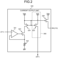
- FIG. 2 is a diagram illustrating a configuration example of the current output unit according to the first embodiment of the present disclosure.
- the drawing is a circuit diagram illustrating a configuration example of the current output unit 320. Note that the current output unit 330 and the like can have the same configuration.
- the current output unit 320 includes an operational amplifier 321, a resistor 322, and MOS transistors 323 to 326.
- MOS transistor 323 an n-channel MOS transistor can be applied.
- a p-channel MOS transistor can be applied to the MOS transistors 324 to 326.
- a power supply line Vdd is arranged in the current output unit 320.
- a signal line from the digital-to-analog conversion unit 311 is connected to a non-inverting input of the operational amplifier 321.
- An output of the operational amplifier 321 is connected to a gate of the MOS transistor 323.
- a source of the MOS transistor 323 is connected to an inverting input of the operational amplifier 321 and to one end of the resistor 322.
- the other end of the resistor 322 is connected to a common GND.
- a drain of the MOS transistor 323 is connected to a drain of the MOS transistor 324.
- the gate of the MOS transistor 324 is connected to a source of the MOS transistor 324, a gate of the MOS transistor 325, a gate of the MOS transistor 326, and the power supply line Vdd.
- the MOS transistor 325 has a source connected to the power supply line Vdd and a drain connected to a wiring to the switch element 261.
- the MOS transistor 326 has a source connected to the power supply line Vdd and a drain connected to a wiring to the output terminal 210.
- a circuit of the operational amplifier 321, the MOS transistor 323, and the resistor constitute a voltage-current conversion circuit.
- a current according to the output current signal from the digital-to-analog conversion unit 311 is generated on the basis of the resistor 322, and is output as a drain current of the MOS transistor 323.
- the MOS transistor 324 and the MOS transistor 326 constitute a current mirror circuit.
- the MOS transistor 324 has a gate connected to its own source.
- a drain current of the MOS transistor 324 is mirrored to the MOS transistor 326 as a reference current.
- This reference current corresponds to the drain current of the MOS transistor 323. Therefore, a drain current of the MOS transistor 326 becomes a current based on the output current signal.
- a mirror ratio can be set to 1: 1.
- the MOS transistor 324 is an example of a "first transistor" of the present disclosure.
- the MOS transistor 326 is an example of a "second transistor" of the present disclosure.
- the MOS transistor 325 is further connected to the current mirror circuit described above.
- the reference current is also mirrored to the MOS transistor 325. Therefore, a drain current of the MOS transistor 325 also becomes a current based on the output current signal.
- the drain current of the MOS transistor 326 and the drain current of the MOS transistor 325 become currents of a ratio according to the respective channel sizes and the like. Therefore, the drain current of the MOS transistor 325 can be used as an alternative to the drain current of the MOS transistor 326, i.e., as the output current.
- a desired ratio of alternative currents can be generated.
- an alternative current can be generated by a circuit of the MOS transistor 325.
- the circuit including the MOS transistor 325 constitute the alternative current generation unit 390.
- the MOS transistor 325 is an example of a "third transistor" of the present disclosure.
- an alternative current can be generated on the basis of the resistor 322.
- the resistor 322 is arranged also in other current output unit 330 or the like, an alternative current can be generated for each of the current output units 320 to 350. Since the resistor 322 is a resistor formed in the integrated circuit 30 or the like, a variation in a resistance value of the resistor 322 in each current output unit 320 is reduced. Therefore, feedback control can be performed using an alternative current instead of the output current.
- the output current and the alternative current include an error based on the variation of the resistor 322. However, these errors can be reduced (compressed) by an action of a feedback control system including the circuit of the reference resistor 110 of FIG. 1 .
- the current output device 1 selects an alternative current from the plurality of current output units 320 and the like by a circuit of the switch element 261 and the like and inputs the selected alternative current to the circuit of the reference resistor 110 and the analog-to-digital conversion unit 120. Therefore, the configuration of the current output device 1 can be simplified as compared with a case where the circuit of the reference resistor 110 and the analog-to-digital conversion unit 120 are arranged for each channel. This can reduce an increase in cost of the current output device 1.
- the current output device 1 of the first embodiment described above generates an alternative current on the basis of the resistor 322 arranged in the current output unit 320.
- feedback control including the digital-to-analog conversion unit 311 and the like in a loop is performed, there is a problem that a response speed is relatively slow.
- a current output device 1 according to a second embodiment of the present disclosure is different from the above-described first embodiment in that an alternative current is generated on the basis of a resistor arranged in an integrated circuit 30 or the like.
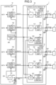
- FIG. 3 is a diagram illustrating a configuration example of the current output device according to the second embodiment of the present disclosure.
- the drawing is a block diagram illustrating a configuration example of the current output device 1 similarly to FIG. 1 .
- the current output device 1 in the drawing is different from the current output device 1 in FIG. 1 in including switch elements 263 and 267 and alternative current generation units 360 and 370 instead of the switch elements 261, 262, 265, and 266.
- the alternative current generation units 360 and 370 generate an alternative current similarly to the alternative current generation unit 390 in FIG. 2 .
- the alternative current generation unit 360 or the like generates an alternative current on the basis of its own resistor.
- the alternative current generation unit 360 is arranged in the integrated circuit 30, and the alternative current generation unit 370 is arranged in an integrated circuit 31. Note that, in the integrated circuit 30, current output units 320 and 330 and the alternative current generation unit 360 are assumed to be configured on the same semiconductor chip. Similarly, in the integrated circuit 31, current output units 340 and 350 and the alternative current generation unit 370 are assumed to be configured on the same semiconductor chip.
- the switch elements 263 and 267 are switches that are arranged in the signal line to which an alternative current is supplied and to which the alternative current is output. Specifically, the switch element 263 corresponds to an alternative current of the alternative current generation unit 360, and the switch element 267 corresponds to an alternative current of the alternative current generation unit 370.
- the alternative current generation unit 390 can be omitted from the current output unit 320 or the like in the drawing.
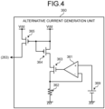
- FIG. 4 is a diagram illustrating a configuration example of the alternative current generation unit according to the second embodiment of the present disclosure.
- the drawing is a circuit diagram illustrating a configuration example of the alternative current generation unit 360. Note that the alternative current generation unit 370 can have the same configuration.
- the alternative current generation unit 360 includes an operational amplifier 361, a resistor 362, MOS transistors 363 to 365, and a voltage source 369.
- MOS transistor 363 an n-channel MOS transistor can be applied.
- MOS transistors 364 and 365 a p-channel MOS transistor can be applied.
- a power supply line Vdd is arranged in the alternative current generation unit 360.
- the voltage source 369 has a low potential side terminal connected to a common GND and a high potential side terminal connected to a non-inverting input of the operational amplifier 361.
- the operational amplifier 361 has an output connected to a gate of the MOS transistor 363.
- the MOS transistor 363 has a source connected to an inverting input of the operational amplifier 361 and to one end of the resistor 362.
- the resistor 362 has the other end connected to the common GND.
- the MOS transistor 363 has a drain connected to a drain of the MOS transistor 364.
- the MOS transistor 364 has a gate connected to a source of the MOS transistor 364, a gate of the MOS transistor 365, and the power supply line Vdd.
- the MOS transistor 365 has a source connected to the power supply line Vdd, and a drain connected to a wiring to the switch element 263.
- the MOS transistors 364 and 365 constitute a current mirror circuit. Furthermore, a circuit of the operational amplifier 361, the MOS transistor 363, and the resistor 362 constitute a voltage-current conversion circuit. An output voltage of the voltage source 369 corresponds to the reference voltage. A drain current of the MOS transistor 363 becomes a current based on a voltage of the voltage source 369 and the resistor 362. This drain current becomes a reference current of the current mirror circuit and is mirrored to the MOS transistor 365. A drain current of the MOS transistor 365 is output as an alternative current. Since the resistor 362 is a resistor arranged in an integrated circuit 30 which also includes the resistor 322 of the current output unit 320, it has characteristics similar to those of the resistor 322.
- a variation in resistance values of the resistor 362 and the resistor 322 is reduced.
- a change in the resistance value due to a temperature drift of each of the resistor 362 and the resistor 322 is also substantially equal. Therefore, instead of the alternative current based on the resistor 322, a current based on the resistor 362 can be used as an alternative current.
- an alternative current can be generated on the basis of the resistor 362. Since the resistor 362 does not require a resistor with high accuracy, an increase in cost of the current output device 1 can be reduced.
- an alternative current from the integrated circuit 30 or the like is selected by circuits of the switch elements 263 and 267 and input to the circuit of the reference resistor 110 and to the analog-to-digital conversion unit 120. Therefore, the configuration of the current output device 1 can be simplified as compared with a case where the circuit of the reference resistor 110 and the analog-to-digital conversion unit 120 are arranged for each channel.
- the digital-to-analog conversion unit 311 is not included in a control system as compared with the current output device 1 of FIG. 1 , the current output device 1 according to the second embodiment of the present disclosure can improve a response speed.
- the remaining configurations of the current output device 1 are similar to those of the current output device 1 according to the first embodiment of the present disclosure, and thus description thereof will be omitted.
- FIG. 5 is a diagram illustrating a configuration example of a current output device according to a third embodiment of the present disclosure.
- the drawing is a block diagram illustrating a configuration example of the current output device 1 similarly to FIG. 1 .
- the current output device 1 in the drawing is different from the current output device 1 of FIG. 1 in further including switch elements 263 and 267 and alternative current generation units 360 and 370.
- the current output device 1 in the drawing includes the alternative current generation unit 390 in FIG. 2 and the alternative current generation units 360 and 370. Therefore, the current output device 1 in the drawing can selectively use an alternative current generated by the alternative current generation unit 390 and the alternative current generation units 360 and 370. For example, in a case where an output current is controlled with relatively high accuracy, an alternative current from the alternative current generation unit 390 arranged for each current output unit 320 can be selected, and in a case where a relatively quick response is required, an alternative current from the alternative current generation unit 360 or the like can be selected.
- the remaining configurations of the current output device 1 are similar to those of the current output device 1 according to the first embodiment of the present disclosure, and thus description thereof will be omitted.
Landscapes
- Engineering & Computer Science (AREA)
- Power Engineering (AREA)
- Physics & Mathematics (AREA)
- Electromagnetism (AREA)
- General Physics & Mathematics (AREA)
- Radar, Positioning & Navigation (AREA)
- Automation & Control Theory (AREA)
- Control Of Electrical Variables (AREA)
- Analogue/Digital Conversion (AREA)
Abstract
A current output device (1) has a plurality of current output units (320, 330, 340, 350), an alternative current generation unit (390), a signal conversion unit, and an output current correction unit (101, 102, 103, 104). The current output unit (320, 330, 340, 350) outputs, to an external circuit, an output current based on an output current signal that is input. The alternative current generation unit (390) generates an alternative current, which is a current that substitutes for the output current of the current output unit (320, 330, 340, 350), on the basis of a resistor (322) arranged in an integrated circuit (30, 31) which also includes the current output units (320, 330, 340, 350). The signal conversion unit converts the alternative current into a voltage signal on the basis of a reference resistor (110). The output current correction unit (101, 102, 103, 104) is arranged for each of the current output units (320, 330, 340, 350) and generates the output current signal on the basis of a difference between the voltage signal and a target value.
Description
- The present disclosure relates to a current output device.
- Conventionally, a current output device that supplies a predetermined current for use in signal transmission or the like to a field device or the like has been used in a plant or a factory. For example, there has been proposed a current output module that generates a voltage according to an output current using a reference resistor, compares the voltage with a reference voltage, and controls the output current on the basis of a comparison result (see, for example,
JP 2022-141251 A - The current output module described above uses a reference resistor to detect an output current. This reference resistor is required to have relatively high accuracy. This is to reduce an error in detection of an output current.
- However, in the above-described conventional technique, there is a problem that a highly accurate reference resistor is required for each channel in a case of being applied to a multi-channel current output device that simultaneously outputs a plurality of currents. For this reason, with the above-described conventional technique, there arises a problem of a cost increase.
- The present disclosure provides a technique for simplifying a current output device that stabilizes a plurality of output currents.
- It is an object of the present invention to at least partially solve the problems in the conventional technology.
- A current output device according to the present disclosure includes a plurality of current output units, an alternative current generation unit, a signal conversion unit and an output current correction unit. The current output unit outputs, to an external circuit, an output current based on an output current signal that is input. The alternative current generation unit generates an alternative current on the basis of a resistor arranged in an integrated circuit which also includes the current output units, the alternative current being a current that substitutes for the output current of the current output units. The signal conversion unit converts the alternative current into a voltage signal on the basis of a reference resistor. The output current correction unit is arranged for each of the current output units and generates the output current signal on the basis of a difference between the voltage signal and a target value.
- The above and other objects, features, advantages and technical and industrial significance of this invention will be better understood by reading the following detailed description of presently preferred embodiments of the invention, when considered in connection with the accompanying drawings.
-
-
FIG. 1 is a diagram illustrating a configuration example of a current output device according to a first embodiment of the present disclosure; -
FIG. 2 is a diagram illustrating a configuration example of a current output unit according to the first embodiment of the present disclosure; -
FIG. 3 is a diagram illustrating a configuration example of a current output device according to a second embodiment of the present disclosure; -
FIG. 4 is a diagram illustrating a configuration example of an alternative current generation unit according to the second embodiment of the present disclosure; and -
FIG. 5 is a diagram illustrating a configuration example of a current output device according to a third embodiment of the present disclosure. - In the following, embodiments of the present disclosure will be described in detail with reference to the drawings. The description will be given in the following order. In each of the following embodiments, the same parts are denoted by the same reference numerals to omit redundant description.
- 1. First Embodiment
- 2. Second Embodiment
- 3. Third Embodiment
-
FIG. 1 is a diagram illustrating a configuration example of a current output device according to a first embodiment of the present disclosure. The drawing is a block diagram illustrating a configuration example of acurrent output device 1. Thecurrent output device 1 individually outputs a current to a plurality of field devices. Thecurrent output device 1 in the drawing includes four-channel current output units.Field devices 2 to 5 are illustrated in the drawing. Thecurrent output device 1 can individually output a predetermined current to thefield devices 2 to 5. - The
current output device 1 includes acontrol unit 10 and acurrent output module 20. Thecontrol unit 10 controls an output current of thecurrent output module 20. Thecontrol unit 10 outputs output current signals (DOUT1 to DOUT4 in the drawing) that are control signals for the channels of thecurrent output module 20, respectively. In addition, thecontrol unit 10 performs feedback control on the basis of a current (alternative current to be described later) according to the output current for each channel from thecurrent output module 20 to stabilize the output current of thecurrent output module 20. - In addition, the
current output module 20 generates a current for each channel and outputs the current to thefield device 2 or the like via an output terminal. Thecurrent output module 20 in the drawing includes anoutput terminal 210, anoutput terminal 220, anoutput terminal 230, and anoutput terminal 240. Theoutput terminal 210 is connected to thefield device 2 to supply a current (IOUT1). Theoutput terminal 220 is connected to thefield device 3 to supply a current (IOUT2). Theoutput terminal 230 is connected to thefield device 4 to supply a current (IOUT3). Theoutput terminal 240 is connected to thefield device 5 to supply a current (IOUT4). In addition, in thecurrent output module 20, a current output unit (acurrent output unit 320 or the like to be described later) corresponding to each of theoutput terminals 210 to 240 is arranged. Thecurrent output unit 320 and the like are connected to theoutput terminal 210 and the like, respectively. For example, one end of theoutput terminal 210 is connected to thecurrent output unit 320, and the other end of theoutput terminal 210 is connected to a common GND. - The
control unit 10 includes a plurality of output current correction units (outputcurrent correction units 101 to 104), areference resistor 110, an analog-to-digital conversion unit 120, and aselection control unit 268. In this drawing, the "analog-to-digital conversion unit" is described as "A/D". - The output
current correction unit 101 and the like are each arranged for each channel and output the output current signal that is a control signal on the basis of a difference between a target value and a voltage signal (DIN) according to the output current of a channel to which the output current correction unit itself corresponds. In the drawing, "ISET1 ", "ISET2", "ISET3", and "ISET4" represent target values of the outputcurrent correction units 101 to 104, respectively. Furthermore, "DOUT1", "DOUT2", "DOUT3 ", and "DOUT4" represent the output current signals of the outputcurrent correction units 101 to 104, respectively. Note that the outputcurrent correction unit 101 and the like in the drawing generate a digital output current signal. The outputcurrent correction unit 101 and the like control thecurrent output unit 320 and the like so as to reduce the difference between the voltage signal (DIN) according to the output current and the target value. - The
reference resistor 110 converts an alternative current (IVAL) output from thecurrent output module 20 into a voltage signal (VVAL). Here, the alternative current is a current corresponding to the output current of thecurrent output unit 320 or the like, and is a current that substitutes for the output current. The voltage signal (VVAL) can be generated by passing the alternative current through thereference resistor 110. Note that a circuit of thereference resistor 110 is an example of a "signal conversion unit" of the present disclosure. - The analog-to-
digital conversion unit 120 performs analog-to-digital conversion on the above-described voltage signal (VVAL) to generate the voltage signal (DIN). - The
selection control unit 268 controls selection of an alternative current in thecurrent output module 20. The above-described alternative current is generated for each ofcurrent output units 320 to 350. One of the plurality of alternative currents is selected and output from thecurrent output module 20. Theselection control unit 268 controls the selection of the alternative current. - The
current output module 20 includes the above-describedoutput terminals 210 to 240, a plurality of digital-to-analog conversion units (digital-to-analog conversion units 311 to 314), and the plurality of current output units (thecurrent output unit 320, thecurrent output unit 330, thecurrent output unit 340, and the current output unit 350). In this drawing, the "digital-to-analog conversion unit" is described as "D/A". In addition, thecurrent output module 20 further includes a plurality of alternative current generation units (an alternativecurrent generation unit 390 to be described later) and switchelements current output units analog conversion units switch elements integrated circuit 30. In addition, thecurrent output units analog conversion units switch elements integrated circuit 31. - The digital-to-
analog conversion unit 311 and the like convert a digital output current signal output from the outputcurrent correction unit 101 and the like into an analog output current signal. The converted output current signal is output to thecurrent output unit 320 or the like. Specifically, the digital-to-analog conversion unit 311 converts the DOUT1 into an analog signal and outputs the analog signal to thecurrent output unit 320. The digital-to-analog conversion unit 312 converts the DOUT2 into an analog signal and outputs the analog signal to thecurrent output unit 330. The digital-to-analog conversion unit 313 converts the DOUT3 into an analog signal and outputs the analog signal to thecurrent output unit 340. The digital-to-analog conversion unit 314 converts the DOUT4 into an analog signal and outputs the analog signal to thecurrent output unit 350. Note that the digital-to-analog conversion units integrated circuit 30. Similarly, the digital-to-analog conversion units integrated circuit 31. - The
current output unit 320 or the like generates an output current on the basis of an output current signal and outputs the output current to thefield device 2 or the like via theoutput terminal 210 or the like. Specifically, thecurrent output unit 320 outputs a current via theoutput terminal 210. Thecurrent output unit 330 outputs a current via theoutput terminal 220. Thecurrent output unit 340 outputs a current via theoutput terminal 230. Thecurrent output unit 350 outputs a current via theoutput terminal 240. In addition, thecurrent output unit 320 and the like generate alternative currents of their own output currents, respectively. Details of the configuration of thecurrent output unit 320 and the like will be described later. - The
switch element 261 or the like is a switch that is arranged on a signal line to which an alternative current is supplied and that causes the alternative current to be output. Specifically, theswitch element 261 corresponds to an alternative current of thecurrent output unit 320, theswitch element 262 corresponds to an alternative current of thecurrent output unit 330, theswitch element 265 corresponds to an alternative current of thecurrent output unit 340, and theswitch element 266 corresponds to an alternative current of thecurrent output unit 350. An alternative current can be selected by conducting electricity to any of theseswitch elements 261 and the like. The selected alternative current is output from thecurrent output module 20 as the above-described IVAL. Theselection control unit 268 controls electrical continuity of theswitch elements switch element 261 and the like. Note that theselection control unit 268 and circuits of theswitch elements - An alternative current of a channel selected by the
selection control unit 268, theswitch element 261, and the like is fed back to the corresponding outputcurrent correction unit 101 and the like via thereference resistor 110 and the analog-to-digital conversion unit 120 to correct an output current. By performing this procedure sequentially for all the channels, accuracy of the output currents IOUT1 to IOUT4 can be improved. -
FIG. 2 is a diagram illustrating a configuration example of the current output unit according to the first embodiment of the present disclosure. The drawing is a circuit diagram illustrating a configuration example of thecurrent output unit 320. Note that thecurrent output unit 330 and the like can have the same configuration. - The
current output unit 320 includes anoperational amplifier 321, aresistor 322, andMOS transistors 323 to 326. As theMOS transistor 323, an n-channel MOS transistor can be applied. Furthermore, a p-channel MOS transistor can be applied to theMOS transistors 324 to 326. In addition, a power supply line Vdd is arranged in thecurrent output unit 320. - A signal line from the digital-to-
analog conversion unit 311 is connected to a non-inverting input of theoperational amplifier 321. An output of theoperational amplifier 321 is connected to a gate of theMOS transistor 323. A source of theMOS transistor 323 is connected to an inverting input of theoperational amplifier 321 and to one end of theresistor 322. The other end of theresistor 322 is connected to a common GND. A drain of theMOS transistor 323 is connected to a drain of theMOS transistor 324. The gate of theMOS transistor 324 is connected to a source of theMOS transistor 324, a gate of theMOS transistor 325, a gate of theMOS transistor 326, and the power supply line Vdd. TheMOS transistor 325 has a source connected to the power supply line Vdd and a drain connected to a wiring to theswitch element 261. TheMOS transistor 326 has a source connected to the power supply line Vdd and a drain connected to a wiring to theoutput terminal 210. - A circuit of the
operational amplifier 321, theMOS transistor 323, and the resistor constitute a voltage-current conversion circuit. A current according to the output current signal from the digital-to-analog conversion unit 311 is generated on the basis of theresistor 322, and is output as a drain current of theMOS transistor 323. - The
MOS transistor 324 and theMOS transistor 326 constitute a current mirror circuit. TheMOS transistor 324 has a gate connected to its own source. A drain current of theMOS transistor 324 is mirrored to theMOS transistor 326 as a reference current. This reference current corresponds to the drain current of theMOS transistor 323. Therefore, a drain current of theMOS transistor 326 becomes a current based on the output current signal. By equalizing channel sizes of theMOS transistor 324 and theMOS transistor 326, a mirror ratio can be set to 1: 1. Note that theMOS transistor 324 is an example of a "first transistor" of the present disclosure. TheMOS transistor 326 is an example of a "second transistor" of the present disclosure. - Furthermore, the
MOS transistor 325 is further connected to the current mirror circuit described above. The reference current is also mirrored to theMOS transistor 325. Therefore, a drain current of theMOS transistor 325 also becomes a current based on the output current signal. In addition, the drain current of theMOS transistor 326 and the drain current of theMOS transistor 325 become currents of a ratio according to the respective channel sizes and the like. Therefore, the drain current of theMOS transistor 325 can be used as an alternative to the drain current of theMOS transistor 326, i.e., as the output current. By changing the size of the channel of theMOS transistor 325 with respect to the channel size of theMOS transistor 324, a desired ratio of alternative currents can be generated. Thus, an alternative current can be generated by a circuit of theMOS transistor 325. Note that the circuit including theMOS transistor 325 constitute the alternativecurrent generation unit 390. TheMOS transistor 325 is an example of a "third transistor" of the present disclosure. - In this manner, an alternative current can be generated on the basis of the
resistor 322. Furthermore, since theresistor 322 is arranged also in othercurrent output unit 330 or the like, an alternative current can be generated for each of thecurrent output units 320 to 350. Since theresistor 322 is a resistor formed in theintegrated circuit 30 or the like, a variation in a resistance value of theresistor 322 in eachcurrent output unit 320 is reduced. Therefore, feedback control can be performed using an alternative current instead of the output current. In addition, the output current and the alternative current include an error based on the variation of theresistor 322. However, these errors can be reduced (compressed) by an action of a feedback control system including the circuit of thereference resistor 110 ofFIG. 1 . Note that in order to reduce an error of the feedback control system, it is necessary to use a resistor with high accuracy as thereference resistor 110 inFIG. 1 . However, a highly accurate resistor is not required for the plurality ofresistors 322. Therefore, an increase in cost of thecurrent output device 1 can be reduced. - In addition, the
current output device 1 selects an alternative current from the plurality ofcurrent output units 320 and the like by a circuit of theswitch element 261 and the like and inputs the selected alternative current to the circuit of thereference resistor 110 and the analog-to-digital conversion unit 120. Therefore, the configuration of thecurrent output device 1 can be simplified as compared with a case where the circuit of thereference resistor 110 and the analog-to-digital conversion unit 120 are arranged for each channel. This can reduce an increase in cost of thecurrent output device 1. - The
current output device 1 of the first embodiment described above generates an alternative current on the basis of theresistor 322 arranged in thecurrent output unit 320. In addition, since feedback control including the digital-to-analog conversion unit 311 and the like in a loop is performed, there is a problem that a response speed is relatively slow. By contrast, acurrent output device 1 according to a second embodiment of the present disclosure is different from the above-described first embodiment in that an alternative current is generated on the basis of a resistor arranged in anintegrated circuit 30 or the like. -
FIG. 3 is a diagram illustrating a configuration example of the current output device according to the second embodiment of the present disclosure. The drawing is a block diagram illustrating a configuration example of thecurrent output device 1 similarly toFIG. 1 . Thecurrent output device 1 in the drawing is different from thecurrent output device 1 inFIG. 1 in includingswitch elements current generation units switch elements - The alternative
current generation units current generation unit 390 inFIG. 2 . The alternativecurrent generation unit 360 or the like generates an alternative current on the basis of its own resistor. The alternativecurrent generation unit 360 is arranged in theintegrated circuit 30, and the alternativecurrent generation unit 370 is arranged in anintegrated circuit 31. Note that, in theintegrated circuit 30,current output units current generation unit 360 are assumed to be configured on the same semiconductor chip. Similarly, in theintegrated circuit 31,current output units current generation unit 370 are assumed to be configured on the same semiconductor chip. - The
switch elements switch element 263 corresponds to an alternative current of the alternativecurrent generation unit 360, and theswitch element 267 corresponds to an alternative current of the alternativecurrent generation unit 370. - Note that the alternative
current generation unit 390 can be omitted from thecurrent output unit 320 or the like in the drawing. -
FIG. 4 is a diagram illustrating a configuration example of the alternative current generation unit according to the second embodiment of the present disclosure. The drawing is a circuit diagram illustrating a configuration example of the alternativecurrent generation unit 360. Note that the alternativecurrent generation unit 370 can have the same configuration. - The alternative
current generation unit 360 includes anoperational amplifier 361, aresistor 362,MOS transistors 363 to 365, and avoltage source 369. As theMOS transistor 363, an n-channel MOS transistor can be applied. As theMOS transistors current generation unit 360, a power supply line Vdd is arranged. - The
voltage source 369 has a low potential side terminal connected to a common GND and a high potential side terminal connected to a non-inverting input of theoperational amplifier 361. Theoperational amplifier 361 has an output connected to a gate of theMOS transistor 363. TheMOS transistor 363 has a source connected to an inverting input of theoperational amplifier 361 and to one end of theresistor 362. Theresistor 362 has the other end connected to the common GND. TheMOS transistor 363 has a drain connected to a drain of theMOS transistor 364. TheMOS transistor 364 has a gate connected to a source of theMOS transistor 364, a gate of theMOS transistor 365, and the power supply line Vdd. TheMOS transistor 365 has a source connected to the power supply line Vdd, and a drain connected to a wiring to theswitch element 263. - The
MOS transistors operational amplifier 361, theMOS transistor 363, and theresistor 362 constitute a voltage-current conversion circuit. An output voltage of thevoltage source 369 corresponds to the reference voltage. A drain current of theMOS transistor 363 becomes a current based on a voltage of thevoltage source 369 and theresistor 362. This drain current becomes a reference current of the current mirror circuit and is mirrored to theMOS transistor 365. A drain current of theMOS transistor 365 is output as an alternative current. Since theresistor 362 is a resistor arranged in anintegrated circuit 30 which also includes theresistor 322 of thecurrent output unit 320, it has characteristics similar to those of theresistor 322. Specifically, a variation in resistance values of theresistor 362 and theresistor 322 is reduced. In addition, a change in the resistance value due to a temperature drift of each of theresistor 362 and theresistor 322 is also substantially equal. Therefore, instead of the alternative current based on theresistor 322, a current based on theresistor 362 can be used as an alternative current. - In this manner, an alternative current can be generated on the basis of the
resistor 362. Since theresistor 362 does not require a resistor with high accuracy, an increase in cost of thecurrent output device 1 can be reduced. In addition, an alternative current from the integratedcircuit 30 or the like is selected by circuits of theswitch elements reference resistor 110 and to the analog-to-digital conversion unit 120. Therefore, the configuration of thecurrent output device 1 can be simplified as compared with a case where the circuit of thereference resistor 110 and the analog-to-digital conversion unit 120 are arranged for each channel. In addition, since the digital-to-analog conversion unit 311 is not included in a control system as compared with thecurrent output device 1 ofFIG. 1 , thecurrent output device 1 according to the second embodiment of the present disclosure can improve a response speed. - The remaining configurations of the
current output device 1 are similar to those of thecurrent output device 1 according to the first embodiment of the present disclosure, and thus description thereof will be omitted. - Description will be made of a modification of the
current output device 1 of the first embodiment described above. -
FIG. 5 is a diagram illustrating a configuration example of a current output device according to a third embodiment of the present disclosure. The drawing is a block diagram illustrating a configuration example of thecurrent output device 1 similarly toFIG. 1 . Thecurrent output device 1 in the drawing
is different from thecurrent output device 1 ofFIG. 1 in further includingswitch elements current generation units - The
current output device 1 in the drawing includes the alternativecurrent generation unit 390 inFIG. 2 and the alternativecurrent generation units current output device 1 in the drawing can selectively use an alternative current generated by the alternativecurrent generation unit 390 and the alternativecurrent generation units current generation unit 390 arranged for eachcurrent output unit 320 can be selected, and in a case where a relatively quick response is required, an alternative current from the alternativecurrent generation unit 360 or the like can be selected. - The remaining configurations of the
current output device 1 are similar to those of thecurrent output device 1 according to the first embodiment of the present disclosure, and thus description thereof will be omitted. - Although the embodiments of the present disclosure have been described in the foregoing, the technical scope of the present disclosure is not limited to the above-described embodiments as they are, and various modifications can be made without departing from the gist of the present disclosure. In addition, the components of different embodiments and modifications may be appropriately combined.
- Note that the effects recited in the present specification are merely examples and are not limited, and other effects may be provided.
- Although the invention has been described with respect to specific embodiments for a complete and clear disclosure, the appended claims are not to be thus limited but are to be construed as embodying all modifications and alternative constructions that may occur to one skilled in the art that fairly fall within the basic teaching herein set forth.
- Some examples of combinations of the disclosed technical features are recited below.
- (1) A current output device comprising:
- a plurality of current output units that outputs, to an external circuit, an output current based on an output current signal that is input;
- an alternative current generation unit that generates an alternative current on the basis of a resistor arranged in an integrated circuit which also includes the current output units, the alternative current being a current that substitutes for the output current of the current output units;
- a signal conversion unit that converts the alternative current into a voltage signal on the basis of a reference resistor; and
- an output current correction unit that is arranged for each of the current output units and generates the output current signal on the basis of a difference between the voltage signal and a target value.
- (2) The current output device according to the above (1), further comprising a plurality of the alternative current generation units.
- (3) The current output device according to the above (2), further comprising
- a selection unit that selects a plurality of the alternative currents respectively generated by the plurality of alternative current generation units, wherein
- the signal conversion unit converts the alternative current selected by the selection unit into the voltage signal.
- (4) The current output device according to any one of the above (1) to (3), wherein
- the resistor is arranged in each of the current output units, and
- the current output unit includes a current mirror circuit having a first transistor in which a reference current flows and a second transistor in which the output current obtained by mirroring of the reference current flows, and a current generated on the basis of the output current signal and the resistor is supplied to the current mirror circuit as the reference current.
- (5) The current output device according to the above (4), wherein the alternative current generation unit includes a third transistor that is connected to the current mirror circuit to mirror the reference current.
- (6) The current output device according to any one of the above (1) to (3), wherein the alternative current generation unit generates the alternative current on the basis of a predetermined reference voltage and the resistor.
Claims (6)
- A current output device comprising:a plurality of current output units that outputs, to an external circuit, an output current based on an output current signal that is input;an alternative current generation unit that generates an alternative current on the basis of a resistor arranged in an integrated circuit which also includes the current output units, the alternative current being a current that substitutes for the output current of the current output units;a signal conversion unit that converts the alternative current into a voltage signal on the basis of a reference resistor; andan output current correction unit that is arranged for each of the current output units and generates the output current signal on the basis of a difference between the voltage signal and a target value.
- The current output device according to claim 1, further comprising a plurality of the alternative current generation units.
- The current output device according to claim 2, further comprisinga selection unit that selects a plurality of the alternative currents respectively generated by the plurality of alternative current generation units, whereinthe signal conversion unit converts the alternative current selected by the selection unit into the voltage signal.
- The current output device according to any one of claim 1 to 3, whereinthe resistor is arranged in each of the current output units, andthe current output unit includes a current mirror circuit having a first transistor in which a reference current flows and a second transistor in which the output current obtained by mirroring of the reference current flows, and a current generated on the basis of the output current signal and the resistor is supplied to the current mirror circuit as the reference current.
- The current output device according to claim 4, wherein the alternative current generation unit includes a third transistor that is connected to the current mirror circuit to mirror the reference current.
- The current output device according to any one of claim 1 to 3, wherein the alternative current generation unit generates the alternative current on the basis of a predetermined reference voltage and the resistor.
Applications Claiming Priority (1)
| Application Number | Priority Date | Filing Date | Title |
|---|---|---|---|
| JP2023191706A JP2025079182A (en) | 2023-11-09 | 2023-11-09 | current output device |
Publications (1)
| Publication Number | Publication Date |
|---|---|
| EP4557042A1 true EP4557042A1 (en) | 2025-05-21 |
Family
ID=93430733
Family Applications (1)
| Application Number | Title | Priority Date | Filing Date |
|---|---|---|---|
| EP24210785.2A Pending EP4557042A1 (en) | 2023-11-09 | 2024-11-05 | Current output device |
Country Status (4)
| Country | Link |
|---|---|
| US (1) | US20250158527A1 (en) |
| EP (1) | EP4557042A1 (en) |
| JP (1) | JP2025079182A (en) |
| CN (1) | CN119960541A (en) |
Citations (3)
| Publication number | Priority date | Publication date | Assignee | Title |
|---|---|---|---|---|
| US5155385A (en) * | 1990-02-22 | 1992-10-13 | Fujitsu Limited | Semiconductor integrated circuit device having a bias supply current |
| US20060139065A1 (en) * | 2004-12-24 | 2006-06-29 | Matsushita Electric Industrial Co., Ltd. | Current driver, data driver, display device and current driving method |
| JP2022141251A (en) | 2021-03-15 | 2022-09-29 | 横河電機株式会社 | Current output module |
-
2023
- 2023-11-09 JP JP2023191706A patent/JP2025079182A/en active Pending
-
2024
- 2024-11-04 US US18/936,499 patent/US20250158527A1/en active Pending
- 2024-11-05 EP EP24210785.2A patent/EP4557042A1/en active Pending
- 2024-11-07 CN CN202411580161.2A patent/CN119960541A/en active Pending
Patent Citations (3)
| Publication number | Priority date | Publication date | Assignee | Title |
|---|---|---|---|---|
| US5155385A (en) * | 1990-02-22 | 1992-10-13 | Fujitsu Limited | Semiconductor integrated circuit device having a bias supply current |
| US20060139065A1 (en) * | 2004-12-24 | 2006-06-29 | Matsushita Electric Industrial Co., Ltd. | Current driver, data driver, display device and current driving method |
| JP2022141251A (en) | 2021-03-15 | 2022-09-29 | 横河電機株式会社 | Current output module |
Also Published As
| Publication number | Publication date |
|---|---|
| CN119960541A (en) | 2025-05-09 |
| JP2025079182A (en) | 2025-05-21 |
| US20250158527A1 (en) | 2025-05-15 |
Similar Documents
| Publication | Publication Date | Title |
|---|---|---|
| US20080018324A1 (en) | Voltage-impressed current measuring apparatus and current buffers with switches used therefor | |
| US7696909B2 (en) | Circuit for generating a temperature dependent current with high accuracy | |
| KR940009253B1 (en) | Semiconductor integrated circuit device with bias supply current | |
| US7049985B2 (en) | Method and circuit for producing trimmed voltage using D/A converter circuit | |
| US11899485B2 (en) | Line driver having adjustable current mirror array | |
| US6946848B2 (en) | Calibration configuration | |
| US20210159907A1 (en) | Current steering digital to analog converter (dac) system to perform dac static linearity calibration | |
| CN114740942A (en) | Current calibration circuit | |
| US11209846B2 (en) | Semiconductor device having plural power source voltage generators, and voltage supplying method | |
| US6118262A (en) | Voltage generating circuit and D/A converter | |
| CN115420334B (en) | Monitoring device, electronic device and monitoring method | |
| US20250158527A1 (en) | Current output device | |
| US7663470B2 (en) | Trimming circuit and electronic circuit | |
| KR100936707B1 (en) | Timing calibration circuit and timing calibration method for semiconductor test equipment | |
| JPH1065542A (en) | Analog / digital conversion circuit | |
| JP2008244729A (en) | Terminating resistance adjusting method and terminating resistance adjustment circuit | |
| TWI876642B (en) | Linear regulator device and configuration method thereof | |
| CN115378420B (en) | Level conversion circuit, voltage measurement device, and voltage measurement method | |
| US12556168B2 (en) | Semiconductor integrated circuit and semiconductor device | |
| WO2024208490A1 (en) | Monitoring circuit and corresponding method | |
| US20060164278A1 (en) | A/d converter | |
| JPH04120912A (en) | Multichannel digital/analog converter and test method for the converter | |
| CN119001237A (en) | Internal resistance detection circuit, internal resistance detection method, chip and electronic equipment | |
| JPH1140749A (en) | Reference voltage generation circuit | |
| JP2025084407A (en) | Semiconductor Device |
Legal Events
| Date | Code | Title | Description |
|---|---|---|---|
| PUAI | Public reference made under article 153(3) epc to a published international application that has entered the european phase |
Free format text: ORIGINAL CODE: 0009012 |
|
| STAA | Information on the status of an ep patent application or granted ep patent |
Free format text: STATUS: THE APPLICATION HAS BEEN PUBLISHED |
|
| AK | Designated contracting states |
Kind code of ref document: A1 Designated state(s): AL AT BE BG CH CY CZ DE DK EE ES FI FR GB GR HR HU IE IS IT LI LT LU LV MC ME MK MT NL NO PL PT RO RS SE SI SK SM TR |
|
| STAA | Information on the status of an ep patent application or granted ep patent |
Free format text: STATUS: REQUEST FOR EXAMINATION WAS MADE |
|
| 17P | Request for examination filed |
Effective date: 20251120 |