EP4553902A1 - Silizium-regelgleichrichter integriert mit einem transistor - Google Patents
Silizium-regelgleichrichter integriert mit einem transistor Download PDFInfo
- Publication number
- EP4553902A1 EP4553902A1 EP24172309.7A EP24172309A EP4553902A1 EP 4553902 A1 EP4553902 A1 EP 4553902A1 EP 24172309 A EP24172309 A EP 24172309A EP 4553902 A1 EP4553902 A1 EP 4553902A1
- Authority
- EP
- European Patent Office
- Prior art keywords
- sige
- region
- polysilicon
- regions
- doped
- Prior art date
- Legal status (The legal status is an assumption and is not a legal conclusion. Google has not performed a legal analysis and makes no representation as to the accuracy of the status listed.)
- Pending
Links
Images


Classifications
-
- H—ELECTRICITY
- H10—SEMICONDUCTOR DEVICES; ELECTRIC SOLID-STATE DEVICES NOT OTHERWISE PROVIDED FOR
- H10D—INORGANIC ELECTRIC SEMICONDUCTOR DEVICES
- H10D18/00—Thyristors
- H10D18/251—Lateral thyristors
-
- H—ELECTRICITY
- H10—SEMICONDUCTOR DEVICES; ELECTRIC SOLID-STATE DEVICES NOT OTHERWISE PROVIDED FOR
- H10D—INORGANIC ELECTRIC SEMICONDUCTOR DEVICES
- H10D62/00—Semiconductor bodies, or regions thereof, of devices having potential barriers
- H10D62/10—Shapes, relative sizes or dispositions of the regions of the semiconductor bodies; Shapes of the semiconductor bodies
- H10D62/113—Isolations within a component, i.e. internal isolations
- H10D62/115—Dielectric isolations, e.g. air gaps
-
- H—ELECTRICITY
- H10—SEMICONDUCTOR DEVICES; ELECTRIC SOLID-STATE DEVICES NOT OTHERWISE PROVIDED FOR
- H10D—INORGANIC ELECTRIC SEMICONDUCTOR DEVICES
- H10D89/00—Aspects of integrated devices not covered by groups H10D84/00 - H10D88/00
- H10D89/60—Integrated devices comprising arrangements for electrical or thermal protection, e.g. protection circuits against electrostatic discharge [ESD]
- H10D89/601—Integrated devices comprising arrangements for electrical or thermal protection, e.g. protection circuits against electrostatic discharge [ESD] for devices having insulated gate electrodes, e.g. for IGFETs or IGBTs
- H10D89/711—Integrated devices comprising arrangements for electrical or thermal protection, e.g. protection circuits against electrostatic discharge [ESD] for devices having insulated gate electrodes, e.g. for IGFETs or IGBTs using bipolar transistors as protective elements
- H10D89/713—Integrated devices comprising arrangements for electrical or thermal protection, e.g. protection circuits against electrostatic discharge [ESD] for devices having insulated gate electrodes, e.g. for IGFETs or IGBTs using bipolar transistors as protective elements including a PNP transistor and a NPN transistor, wherein each of said transistors has its base region coupled to the collector region of the other transistor, e.g. silicon controlled rectifier [SCR] devices
-
- H—ELECTRICITY
- H10—SEMICONDUCTOR DEVICES; ELECTRIC SOLID-STATE DEVICES NOT OTHERWISE PROVIDED FOR
- H10D—INORGANIC ELECTRIC SEMICONDUCTOR DEVICES
- H10D62/00—Semiconductor bodies, or regions thereof, of devices having potential barriers
- H10D62/80—Semiconductor bodies, or regions thereof, of devices having potential barriers characterised by the materials
- H10D62/82—Heterojunctions
- H10D62/822—Heterojunctions comprising only Group IV materials heterojunctions, e.g. Si/Ge heterojunctions
-
- H—ELECTRICITY
- H10—SEMICONDUCTOR DEVICES; ELECTRIC SOLID-STATE DEVICES NOT OTHERWISE PROVIDED FOR
- H10D—INORGANIC ELECTRIC SEMICONDUCTOR DEVICES
- H10D84/00—Integrated devices formed in or on semiconductor substrates that comprise only semiconducting layers, e.g. on Si wafers or on GaAs-on-Si wafers
- H10D84/101—Integrated devices comprising main components and built-in components, e.g. IGBT having built-in freewheel diode
- H10D84/131—Thyristors having built-in components
Definitions
- the present disclosure relates to semiconductor structures and, more particularly, to a silicon control rectifier (SCR) integrated with a transistor and methods of manufacture.
- SCR silicon control rectifier
- SCRs are used for electrostatic discharge (ESD) protection of integrated circuits (ICs) from the sudden flow of electricity caused by, for example, contact, electrical shorts, or dielectric breakdown. Because of high current handling ability per unit area of an SCR, ESD devices utilizing SCR can protect ICs from failure. These devices are most often used in high performance analog and radiofrequency (RF) designs for chips that have large signal swings, low leakage, and low capacitance. Due to the capacitance loading and poor harmonics of SCRs, RF performance may be impacted.
- RF radiofrequency
- a structure comprises: a doped region in a semiconductor substrate; at least two regions of semiconductor material comprising opposite doping types over the doped region; and polysilicon regions over respective ones of the least two regions of semiconductor material. Additional features of the structure are set forth in dependent claims 2 to 10.
- a structure comprises: a first doped region of a first dopant type in a semiconductor substrate; a first semiconductor layer over the first doped region and have a first dopant type; a second semiconductor layer over the first doped region and have a second dopant type, opposite to the first dopant type; and polysilicon regions contacting the first semiconductor layer and the second semiconductor layer. Additional features of the structure are set forth in dependent claims 12 to 14.
- a method comprises: forming a doped region in a semiconductor substrate; forming at least two regions of semiconductor material comprising opposite doping types over the doped region; and forming polysilicon regions over respective ones of the least two regions of semiconductor material.
- the present disclosure relates to semiconductor structures and, more particularly, to a silicon control rectifier (SCR) and methods of manufacture.
- the SCR includes a doped collector region, semiconductor regions of opposite dopant types formed on top of the doped collector region and separated by dielectric material, and an anode and cathode formed on doped polysilicon regions connecting to the semiconductor regions of opposite dopant types.
- the structures described herein exhibit lowered capacitance with less RF degradation, improved space savings, faster switching times and higher current drive due to more efficient bipolars and vertical integration.
- an SCR comprises an n-type region bounded by shallow trench isolation regions.
- Doped SiGe regions of opposite dopant types may be formed on top of the n-type region and separated by dielectric material.
- An anode and cathode are formed on n+ polysilicon and p+ polysilicon, contacting the SiGe regions of opposite dopant types.
- the SiGe regions of opposite dopant types may be, for example, p-SiGe and n-SiGe layers.
- ohmic contacts to p-SiGe and n-SiGe through the polysilicon regions may be parallel orthogonal to the anode/cathode.
- the structures of the present disclosure can be manufactured in a number of ways using a number of different tools.
- the methodologies and tools are used to form structures with dimensions in the micrometer and nanometer scale.
- the methodologies, i.e., technologies, employed to manufacture the structures of the present disclosure have been adopted from integrated circuit (IC) technology.
- the structures are built on wafers and are realized in films of material patterned by photolithographic processes on the top of a wafer.
- the fabrication of the structures uses three basic building blocks: (i) deposition of thin films of material on a substrate, (ii) applying a patterned mask on top of the films by photolithographic imaging, and (iii) etching the films selectively to the mask.
- precleaning processes may be used to clean etched surfaces of any contaminants, as is known in the art.
- rapid thermal anneal processes may be used to drive-in dopants or material layers as is known in the art.
- FIG. 1A shows a top view of an SCR in a PNPN configuration and respective fabrication processes
- FIG. 1B shows a cross-sectional view of the SCR device of FIG. 1A along line X1-X1.
- the structure 100 includes a doped region 16 in a semiconductor substrate 12, p-type semiconductor material 20 and n-type doped semiconductor material 22 contacting the doped region 16, and polysilicon regions 24, 26 contacting the p-type doped semiconductor material 20.
- polysilicon regions 24a, 26a contact the n-type doped semiconductor material 22.
- the p-type doped semiconductor material 20 and n-type doped semiconductor material 22 may be single crystalline p-SiGe material and n-SiGe material, respectively.
- the doped region 16 may be a sub-collector region comprising n-doped semiconductor material.
- the polysilicon regions 24, 24a, 26, 26a may be doped polysilicon between and contacting contacts 28 (i.e., cathodes and anodes) and the respective SiGe regions 20, 22.
- the polysilicon regions 24, 24a, 26, 26a may also partly overlap with the insulator material 18.
- the polysilicon regions 24, 24a may comprise p+ type polysilicon and the polysilicon regions 26, 26a may comprise n+ type polysilicon.
- the p-type dopants may be, e.g., Boron (B), and the n-type dopants may be, e.g., Arsenic (As), Phosphorus (P) and Antimony (Sb), among other suitable examples.
- SCR may be an PNPN device.
- the semiconductor substrate 12 may be composed of any suitable semiconductor material including, but not limited to, Si, SiGe, SiGeC, SiC, GaAs, InAs, InP, and other III/V or II/VI compound semiconductors.
- the semiconductor substrate 12 may also comprise any suitable single crystallographic orientation (e.g., a (100), (110), (111), or (001) crystallographic orientation).
- the semiconductor substrate 12 may be a bulk substrate comprising the semiconductor materials described herein or, alternatively, may comprise semiconductor on insulator technology as is known in the art. In the semiconductor on insulator technology, the semiconductor substrate 12 would be a top semiconductor layer over an insulator material and a handle substrate as is known in the art.
- Shallow trench isolation regions 14 are formed within the semiconductor substrate 12, which may be adjacent to and isolate the sub-collector 16.
- the SiGe regions 20, 22 are aligned to the edges of the shallow trench isolation regions 14. That is, in preferred embodiments, the SiGe regions 20, 22 do not overlap with the shallow trench isolation regions 14 such that poly-SiGe layers will not form in the structure 100.
- the position of the p-SiGe region 20 and n-SiGe region 22 may be swapped.
- the insulator material 18 may isolate the p-type doped semiconductor material 20 and n-type doped semiconductor material 22. In further embodiments, the insulator material 18 may be buried oxide material. In addition, the polysilicon regions 24, 26 may be isolated from one another by sidewall spacers 19. The sidewalls spacers 19 may be, for example, nitride material formed by conventional deposition methods (e.g., chemical vapor deposition (CVD), followed by anisotropic etching processes. Contacts 28 (i.e., cathodes and anodes) extend to the polysilicon regions 24, 26.
- CVD chemical vapor deposition
- the contacts 28 are parallel to one another and may be formed of any known conductive material, e.g., Tungsten, Al, Cu lined with TiN or TaN as examples.
- the contacts 20 may be formed in interlevel dielectric material 15 using conventional lithography, etching and deposition methods as is known in the art.
- the sub-collector 16 may be formed by conventional implantation processes as described in more detail as further described with respect to FIG. 4A .
- the shallow trench isolation regions 14 may be formed by conventional lithography, etching, and deposition methods known to those of skill in the art as further described with respect to FIG. 4A .
- the p-type doped semiconductor material 20 and n-type doped semiconductor material 22 may be formed by epitaxial growth processes with a respective in-situ doping process.
- the polysilicon regions 24, 24a, 26, 26a may be formed by epitaxial growth processes with a respective in-situ doping process, over the insulator material 18.
- the p-type dopants may be, e.g., Boron (B), and the n-type dopants may be, e.g., Arsenic (As), Phosphorus (P) and Antimony (Sb), among other suitable examples.
- B Boron
- Sb Antimony
- FIG. 2A shows a top view of an SCR in a bipolar junction transistor (BJT) configuration in accordance with additional aspects of the present disclosure.
- FIG. 2B shows a cross-sectional view of the SCR device of FIG. 2A along line X2-X2 and
- FIG. 2C shows a cross-sectional view of the SCR device of FIG. 2A along line X3-X3.
- the polysilicon regions 24, 26 are in a z-axis orientation relative to the device.
- the ohmic contacts to the p-SiGe material 20 and n-SiGe material 22 through the poly p+ and n+ regions 24, 26 are orthogonal to the anode and cathode.
- FIG. 2B shows the n-type doped polysilicon region 24 provided on and contacting the p-SiGe material 20 and the p-type doped polysilicon region 26 provided on and contacting the n-SiGe material 22.
- FIG. 2C shows the p-type doped polysilicon region 26 provided on and contacting the p-SiGe material 20 and the n-type doped polysilicon region 24 provided on and contacting the n-SiGe material 22.
- the remaining features may also be similar to the structure 100 shown in FIGS. 1A and 1B such that no further explanation is required herein.
- FIG. 3 shows a cross-sectional view of a SCR device in a BJT configuration.
- the structure 300 comprises a p-type doped region 16c in an N-well 16a and adjacent to the n-type doped region 16b (which may be part of the N-well 16a).
- the p-type doped region 16c and the n-type doped region 16b may form a p-n junction.
- the p-type doped polysilicon region 26 may be provided on and contacting the p-SiGe material 20; whereas the n-type doped polysilicon region 24 may be provided on and contacting the n-SiGe material 22.
- Both the p-type doped polysilicon region 26 and the n-type doped polysilicon region 24 may overlap with the insulator material 18.
- the remaining features of the structure 200 may also be similar to the structure 100 shown in FIGS. 1A and 1B such that no further explanation is required herein.
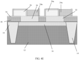
- FIG. 4A-4E show cross-sectional views of steps in the fabrication process of the SCR of FIGS. 1A and 1B in accordance with further aspects of the present disclosure. It should be understood by those of skill in the art that similar processes can also be used to fabricate the SCR structures 200 and 300 by, for example, using different in-situ dopants during epitaxial growth processes as described herein.
- the sub-collector regions may be formed by ion implantation processes as is known in the art such that no further explanation is required for a complete understanding of the present disclosure.
- an n-type sub-collector 16 may be formed in the semiconductor substrate 12.
- a patterned implantation mask is used to select the exposed area for forming the n-type sub-collector 16.
- the implantation mask may include a layer of a light-sensitive material, such as an organic photoresist, applied by a spin coating process, pre-baked, exposed to light projected through a photomask, baked after exposure, and developed with a chemical developer.
- the implantation mask has a thickness and stopping power sufficient to block masked areas against receiving a dose of the implanted ions.
- the n-type dopants may be, e.g., Arsenic (As), Phosphorus (P) and Sb, among other suitable examples.
- the shallow trench isolation regions 14 is formed adjacent to the n-type sub-collector 16.
- the shallow trench isolation regions 14 can be formed by conventional lithography, etching and deposition methods known to those of skill in the art. For example, a resist formed over the semiconductor substrate 12 is exposed to energy (light) and developed utilizing a conventional resist developer to form a pattern (opening). An etching process with a selective chemistry, e.g., reactive ion etching (RIE), will be used to transfer the pattern from the patterned photoresist layer to the semiconductor substrate 12 to form one or more trenches in the semiconductor substrate 12.
- RIE reactive ion etching
- insulator material e.g., SiO 2
- CVD chemical vapor deposition
- Any residual material on the surface of the semiconductor substrate 12 can be removed by conventional chemical mechanical polishing (CMP) processes.
- the p-SiGe material 20 is formed over the n-type sub-collector 16.
- the insulator material 18 is deposited over the semiconductor substrate 12.
- the insulator material 18 may be deposited by any conventional deposition method, e.g., CVD.
- a masking layer 34 is deposited on the insulator material 18.
- the masking layer 34 may be nitride, deposited by a conventional deposition method, e.g., CVD.
- An opening is formed through the insulator material 18 and masking layer 34 to expose the underlying n-type sub-collector 16.
- the opening may be formed by conventional lithography and etching processes as is known in the art.
- a SiGe material is epitaxially grown on the exposed underlying n-type sub-collector 16.
- the epitaxial growth process includes an in-situ doping process with a p-type dopant to form the p-SiGe material 20.
- the n-SiGe material 22 is formed over the n-type sub-collector 16.
- insulator material 36 and masking layer 38 are formed over masking layer 34 using any conventional deposition method, e.g., CVD.
- the insulator material 36 may also be oxide and the masking layer 38 may also be nitride.
- An opening is formed through the insulator materials 18, 36 and masking layers 34, 38 to expose the underlying n-type sub-collector 16, again using conventional lithography and etching processes.
- a SiGe material is epitaxially grown on the exposed underlying n-type sub-collector 16.
- the epitaxial growth process includes an in-situ doping process with an n-type dopant to form the n-SiGe material 22.
- the insulator materials 18, 36 and masking layer 38 are removed by conventional stripping techniques such as a chemical mechanical polishing (CMP) or etching processes (e.g., reactive ion etching processes with selective chemistries) as is known in the art.
- CMP chemical mechanical polishing
- etching processes e.g., reactive ion etching processes with selective chemistries
- the p+ type polysilicon regions 26, 26a may be formed over the p-SiGe material 20 and the n-SiGe material 22, overlapping with the insulator material 18.
- the epitaxial growth process may include an in-situ doping process with a p-type dopant, e.g., Boron.
- the polysilicon material will form over the insulator material 18.
- a sidewall spacer material 19, e.g., nitride may be deposited and patterned over the p+ type polysilicon regions 26, 26a.
- n+ type polysilicon regions 24, 24a may be formed over the p-SiGe material 20 and the n-SiGe material 22, overlapping with the insulator material 18.
- the epitaxial growth process may include an in-situ doping process with a n-type dopant, e.g., Arsenic. Again, as is known in the art, the polysilicon material will form over the insulator material 18.
- a sidewall spacer material 19, e.g., nitride may be deposited and patterned over the n+ type polysilicon regions 24, 24a.
- the contacts 28 may be formed through interlevel dielectric material 15 by conventional lithography, etching and deposition processes as is known in the art.
- a conventional silicide process may be used to provide silicide contacts to the regions.
- the silicide process begins with deposition of a thin transition metal layer, e.g., nickel, cobalt or titanium, over the exposed regions 24, 24a, 26, 26a. After deposition of the material, the structure is heated allowing the transition metal to react with exposed silicon (or other semiconductor material as described herein) forming a low-resistance transition metal silicide. Following the reaction, any remaining transition metal is removed by chemical etching, leaving silicide contacts in the active regions of the device.
- a thin transition metal layer e.g., nickel, cobalt or titanium
- SoC system on chip
- the SoC is an integrated circuit (also known as a "chip") that integrates all components of an electronic system on a single chip or substrate. As the components are integrated on a single substrate, SoCs consume much less power and take up much less area than multi-chip designs with equivalent functionality. Because of this, SoCs are becoming the dominant force in the mobile computing (such as in Smartphones) and edge computing markets. SoC is also used in embedded systems and the Internet of Things.
- the method(s) as described above is used in the fabrication of integrated circuit chips.
- the resulting integrated circuit chips can be distributed by the fabricator in raw wafer form (that is, as a single wafer that has multiple unpackaged chips), as a bare die, or in a packaged form.
- the chip is mounted in a single chip package (such as a plastic carrier, with leads that are affixed to a motherboard or other higher level carrier) or in a multichip package (such as a ceramic carrier that has either or both surface interconnections or buried interconnections).
- the chip is then integrated with other chips, discrete circuit elements, and/or other signal processing devices as part of either (a) an intermediate product, such as a motherboard, or (b) an end product.
- the end product can be any product that includes integrated circuit chips, ranging from toys and other low-end applications to advanced computer products having a display, a keyboard or other input device, and a central processor.
Landscapes
- Bipolar Transistors (AREA)
- Electrodes Of Semiconductors (AREA)
Applications Claiming Priority (1)
| Application Number | Priority Date | Filing Date | Title |
|---|---|---|---|
| US18/388,441 US20250159999A1 (en) | 2023-11-09 | 2023-11-09 | Silicon control rectifier integrated with a transistor |
Publications (1)
| Publication Number | Publication Date |
|---|---|
| EP4553902A1 true EP4553902A1 (de) | 2025-05-14 |
Family
ID=90904606
Family Applications (1)
| Application Number | Title | Priority Date | Filing Date |
|---|---|---|---|
| EP24172309.7A Pending EP4553902A1 (de) | 2023-11-09 | 2024-04-25 | Silizium-regelgleichrichter integriert mit einem transistor |
Country Status (3)
| Country | Link |
|---|---|
| US (1) | US20250159999A1 (de) |
| EP (1) | EP4553902A1 (de) |
| CN (1) | CN119997533A (de) |
Citations (4)
| Publication number | Priority date | Publication date | Assignee | Title |
|---|---|---|---|---|
| US20030047750A1 (en) * | 2001-09-11 | 2003-03-13 | Sarnoff Corporation | Electrostatic discharge protection silicon controlled rectifier (ESD-SCR) for silicon germanium technologies |
| US20040110353A1 (en) * | 2002-12-09 | 2004-06-10 | Shekar Mallikarjunaswamy | Bipolar junction transistor with reduced parasitic bipolar conduction |
| CN105374816A (zh) * | 2015-12-23 | 2016-03-02 | 电子科技大学 | 一种基于锗硅异质结工艺的双向esd保护器件 |
| WO2020047903A1 (en) * | 2018-09-05 | 2020-03-12 | Hong Kong Applied Science and Technology Research Institute Company Limited | Low-capacitance electro-static-discharge (esd) protection structure with two floating wells |
-
2023
- 2023-11-09 US US18/388,441 patent/US20250159999A1/en active Pending
-
2024
- 2024-04-25 EP EP24172309.7A patent/EP4553902A1/de active Pending
- 2024-09-11 CN CN202411269081.5A patent/CN119997533A/zh active Pending
Patent Citations (4)
| Publication number | Priority date | Publication date | Assignee | Title |
|---|---|---|---|---|
| US20030047750A1 (en) * | 2001-09-11 | 2003-03-13 | Sarnoff Corporation | Electrostatic discharge protection silicon controlled rectifier (ESD-SCR) for silicon germanium technologies |
| US20040110353A1 (en) * | 2002-12-09 | 2004-06-10 | Shekar Mallikarjunaswamy | Bipolar junction transistor with reduced parasitic bipolar conduction |
| CN105374816A (zh) * | 2015-12-23 | 2016-03-02 | 电子科技大学 | 一种基于锗硅异质结工艺的双向esd保护器件 |
| WO2020047903A1 (en) * | 2018-09-05 | 2020-03-12 | Hong Kong Applied Science and Technology Research Institute Company Limited | Low-capacitance electro-static-discharge (esd) protection structure with two floating wells |
Also Published As
| Publication number | Publication date |
|---|---|
| US20250159999A1 (en) | 2025-05-15 |
| CN119997533A (zh) | 2025-05-13 |
Similar Documents
| Publication | Publication Date | Title |
|---|---|---|
| US11430881B2 (en) | Diode triggered compact silicon controlled rectifier | |
| EP4340026A1 (de) | Auslöser für siliciumgesteurte gleichrichter | |
| EP4203068A1 (de) | Bipolartransistoren | |
| EP4579749A1 (de) | Elektrostatische vorrichtung | |
| EP4401138A2 (de) | Elektrostatische vorrichtung | |
| EP4443518A1 (de) | Vorrichtungen mit niedriger kapazität und niedrigem widerstand | |
| EP4553902A1 (de) | Silizium-regelgleichrichter integriert mit einem transistor | |
| EP4567875B1 (de) | Integrierter heteroübergang-bipolartransistor mit siliziumgesteuertem gleichrichter | |
| US20250220940A1 (en) | Device triggered silicon control rectifier | |
| US12336302B1 (en) | Vertical device triggered silicon control rectifier | |
| EP4583664A1 (de) | Transistorgesteuerter siliziumsteuergleichrichter | |
| EP4590087A1 (de) | Silizium-steuergleichrichter | |
| EP4716412A1 (de) | Diodengesteuerter siliziumgleichrichter | |
| EP4421874A1 (de) | Hochleistungsfähige siliciumgesteuerte gleichrichtervorrichtungen | |
| US20240304613A1 (en) | Silicon controlled rectifers with field plate | |
| US20250126817A1 (en) | Silicon controlled rectifiers | |
| EP4428924A1 (de) | Hochleistungsfähige siliciumgesteuerte gleichrichtervorrichtungen | |
| US12550452B2 (en) | Silicon controlled rectifiers | |
| EP4642191A1 (de) | Elektrostatische hochspannungsentladungsvorrichtung | |
| EP4456137A1 (de) | Elektrostatische entladungsvorrichtungen | |
| US20230411384A1 (en) | Electrostatic discharge device with pinch resistor |
Legal Events
| Date | Code | Title | Description |
|---|---|---|---|
| PUAI | Public reference made under article 153(3) epc to a published international application that has entered the european phase |
Free format text: ORIGINAL CODE: 0009012 |
|
| STAA | Information on the status of an ep patent application or granted ep patent |
Free format text: STATUS: THE APPLICATION HAS BEEN PUBLISHED |
|
| AK | Designated contracting states |
Kind code of ref document: A1 Designated state(s): AL AT BE BG CH CY CZ DE DK EE ES FI FR GB GR HR HU IE IS IT LI LT LU LV MC ME MK MT NL NO PL PT RO RS SE SI SK SM TR |
|
| STAA | Information on the status of an ep patent application or granted ep patent |
Free format text: STATUS: REQUEST FOR EXAMINATION WAS MADE |
|
| 17P | Request for examination filed |
Effective date: 20251014 |