EP4553899A1 - Die in die semiconductor device and method therefor - Google Patents
Die in die semiconductor device and method therefor Download PDFInfo
- Publication number
- EP4553899A1 EP4553899A1 EP24211867.7A EP24211867A EP4553899A1 EP 4553899 A1 EP4553899 A1 EP 4553899A1 EP 24211867 A EP24211867 A EP 24211867A EP 4553899 A1 EP4553899 A1 EP 4553899A1
- Authority
- EP
- European Patent Office
- Prior art keywords
- semiconductor die
- cavity
- die
- region
- semiconductor
- Prior art date
- Legal status (The legal status is an assumption and is not a legal conclusion. Google has not performed a legal analysis and makes no representation as to the accuracy of the status listed.)
- Pending
Links
Images




Classifications
-
- H—ELECTRICITY
- H10—SEMICONDUCTOR DEVICES; ELECTRIC SOLID-STATE DEVICES NOT OTHERWISE PROVIDED FOR
- H10W—GENERIC PACKAGES, INTERCONNECTIONS, CONNECTORS OR OTHER CONSTRUCTIONAL DETAILS OF DEVICES COVERED BY CLASS H10
- H10W72/00—Interconnections or connectors in packages
- H10W72/20—Bump connectors, e.g. solder bumps or copper pillars; Dummy bumps; Thermal bumps
-
- H—ELECTRICITY
- H10—SEMICONDUCTOR DEVICES; ELECTRIC SOLID-STATE DEVICES NOT OTHERWISE PROVIDED FOR
- H10W—GENERIC PACKAGES, INTERCONNECTIONS, CONNECTORS OR OTHER CONSTRUCTIONAL DETAILS OF DEVICES COVERED BY CLASS H10
- H10W20/00—Interconnections in chips, wafers or substrates
- H10W20/40—Interconnections external to wafers or substrates, e.g. back-end-of-line [BEOL] metallisations or vias connecting to gate electrodes
- H10W20/41—Interconnections external to wafers or substrates, e.g. back-end-of-line [BEOL] metallisations or vias connecting to gate electrodes characterised by their conductive parts
- H10W20/44—Conductive materials thereof
- H10W20/4403—Conductive materials thereof based on metals, e.g. alloys, metal silicides
- H10W20/4421—Conductive materials thereof based on metals, e.g. alloys, metal silicides the principal metal being copper
-
- H—ELECTRICITY
- H10—SEMICONDUCTOR DEVICES; ELECTRIC SOLID-STATE DEVICES NOT OTHERWISE PROVIDED FOR
- H10W—GENERIC PACKAGES, INTERCONNECTIONS, CONNECTORS OR OTHER CONSTRUCTIONAL DETAILS OF DEVICES COVERED BY CLASS H10
- H10W90/00—Package configurations
-
- H—ELECTRICITY
- H10—SEMICONDUCTOR DEVICES; ELECTRIC SOLID-STATE DEVICES NOT OTHERWISE PROVIDED FOR
- H10W—GENERIC PACKAGES, INTERCONNECTIONS, CONNECTORS OR OTHER CONSTRUCTIONAL DETAILS OF DEVICES COVERED BY CLASS H10
- H10W90/00—Package configurations
- H10W90/20—Configurations of stacked chips
- H10W90/28—Configurations of stacked chips the stacked chips having different sizes, e.g. chip stacks having a pyramidal shape
-
- H—ELECTRICITY
- H10—SEMICONDUCTOR DEVICES; ELECTRIC SOLID-STATE DEVICES NOT OTHERWISE PROVIDED FOR
- H10W—GENERIC PACKAGES, INTERCONNECTIONS, CONNECTORS OR OTHER CONSTRUCTIONAL DETAILS OF DEVICES COVERED BY CLASS H10
- H10W90/00—Package configurations
- H10W90/701—Package configurations characterised by the relative positions of pads or connectors relative to package parts
-
- H—ELECTRICITY
- H10—SEMICONDUCTOR DEVICES; ELECTRIC SOLID-STATE DEVICES NOT OTHERWISE PROVIDED FOR
- H10W—GENERIC PACKAGES, INTERCONNECTIONS, CONNECTORS OR OTHER CONSTRUCTIONAL DETAILS OF DEVICES COVERED BY CLASS H10
- H10W99/00—Subject matter not provided for in other groups of this subclass
-
- H—ELECTRICITY
- H10—SEMICONDUCTOR DEVICES; ELECTRIC SOLID-STATE DEVICES NOT OTHERWISE PROVIDED FOR
- H10W—GENERIC PACKAGES, INTERCONNECTIONS, CONNECTORS OR OTHER CONSTRUCTIONAL DETAILS OF DEVICES COVERED BY CLASS H10
- H10W70/00—Package substrates; Interposers; Redistribution layers [RDL]
- H10W70/60—Insulating or insulated package substrates; Interposers; Redistribution layers
- H10W70/67—Insulating or insulated package substrates; Interposers; Redistribution layers characterised by their insulating layers or insulating parts
- H10W70/68—Shapes or dispositions thereof
- H10W70/682—Shapes or dispositions thereof comprising holes having chips therein
-
- H—ELECTRICITY
- H10—SEMICONDUCTOR DEVICES; ELECTRIC SOLID-STATE DEVICES NOT OTHERWISE PROVIDED FOR
- H10W—GENERIC PACKAGES, INTERCONNECTIONS, CONNECTORS OR OTHER CONSTRUCTIONAL DETAILS OF DEVICES COVERED BY CLASS H10
- H10W72/00—Interconnections or connectors in packages
- H10W72/01—Manufacture or treatment
- H10W72/013—Manufacture or treatment of die-attach connectors
- H10W72/01365—Thermally treating
-
- H—ELECTRICITY
- H10—SEMICONDUCTOR DEVICES; ELECTRIC SOLID-STATE DEVICES NOT OTHERWISE PROVIDED FOR
- H10W—GENERIC PACKAGES, INTERCONNECTIONS, CONNECTORS OR OTHER CONSTRUCTIONAL DETAILS OF DEVICES COVERED BY CLASS H10
- H10W72/00—Interconnections or connectors in packages
- H10W72/071—Connecting or disconnecting
- H10W72/072—Connecting or disconnecting of bump connectors
-
- H—ELECTRICITY
- H10—SEMICONDUCTOR DEVICES; ELECTRIC SOLID-STATE DEVICES NOT OTHERWISE PROVIDED FOR
- H10W—GENERIC PACKAGES, INTERCONNECTIONS, CONNECTORS OR OTHER CONSTRUCTIONAL DETAILS OF DEVICES COVERED BY CLASS H10
- H10W72/00—Interconnections or connectors in packages
- H10W72/071—Connecting or disconnecting
- H10W72/072—Connecting or disconnecting of bump connectors
- H10W72/07231—Techniques
- H10W72/07232—Compression bonding, e.g. thermocompression bonding
-
- H—ELECTRICITY
- H10—SEMICONDUCTOR DEVICES; ELECTRIC SOLID-STATE DEVICES NOT OTHERWISE PROVIDED FOR
- H10W—GENERIC PACKAGES, INTERCONNECTIONS, CONNECTORS OR OTHER CONSTRUCTIONAL DETAILS OF DEVICES COVERED BY CLASS H10
- H10W72/00—Interconnections or connectors in packages
- H10W72/071—Connecting or disconnecting
- H10W72/073—Connecting or disconnecting of die-attach connectors
-
- H—ELECTRICITY
- H10—SEMICONDUCTOR DEVICES; ELECTRIC SOLID-STATE DEVICES NOT OTHERWISE PROVIDED FOR
- H10W—GENERIC PACKAGES, INTERCONNECTIONS, CONNECTORS OR OTHER CONSTRUCTIONAL DETAILS OF DEVICES COVERED BY CLASS H10
- H10W72/00—Interconnections or connectors in packages
- H10W72/071—Connecting or disconnecting
- H10W72/073—Connecting or disconnecting of die-attach connectors
- H10W72/07351—Connecting or disconnecting of die-attach connectors characterised by changes in properties of the die-attach connectors during connecting
- H10W72/07354—Connecting or disconnecting of die-attach connectors characterised by changes in properties of the die-attach connectors during connecting changes in dispositions
-
- H—ELECTRICITY
- H10—SEMICONDUCTOR DEVICES; ELECTRIC SOLID-STATE DEVICES NOT OTHERWISE PROVIDED FOR
- H10W—GENERIC PACKAGES, INTERCONNECTIONS, CONNECTORS OR OTHER CONSTRUCTIONAL DETAILS OF DEVICES COVERED BY CLASS H10
- H10W72/00—Interconnections or connectors in packages
- H10W72/20—Bump connectors, e.g. solder bumps or copper pillars; Dummy bumps; Thermal bumps
- H10W72/221—Structures or relative sizes
- H10W72/222—Multilayered bumps, e.g. a coating on top and side surfaces of a bump core
-
- H—ELECTRICITY
- H10—SEMICONDUCTOR DEVICES; ELECTRIC SOLID-STATE DEVICES NOT OTHERWISE PROVIDED FOR
- H10W—GENERIC PACKAGES, INTERCONNECTIONS, CONNECTORS OR OTHER CONSTRUCTIONAL DETAILS OF DEVICES COVERED BY CLASS H10
- H10W72/00—Interconnections or connectors in packages
- H10W72/20—Bump connectors, e.g. solder bumps or copper pillars; Dummy bumps; Thermal bumps
- H10W72/241—Dispositions, e.g. layouts
-
- H—ELECTRICITY
- H10—SEMICONDUCTOR DEVICES; ELECTRIC SOLID-STATE DEVICES NOT OTHERWISE PROVIDED FOR
- H10W—GENERIC PACKAGES, INTERCONNECTIONS, CONNECTORS OR OTHER CONSTRUCTIONAL DETAILS OF DEVICES COVERED BY CLASS H10
- H10W72/00—Interconnections or connectors in packages
- H10W72/20—Bump connectors, e.g. solder bumps or copper pillars; Dummy bumps; Thermal bumps
- H10W72/251—Materials
- H10W72/252—Materials comprising solid metals or solid metalloids, e.g. PbSn, Ag or Cu
-
- H—ELECTRICITY
- H10—SEMICONDUCTOR DEVICES; ELECTRIC SOLID-STATE DEVICES NOT OTHERWISE PROVIDED FOR
- H10W—GENERIC PACKAGES, INTERCONNECTIONS, CONNECTORS OR OTHER CONSTRUCTIONAL DETAILS OF DEVICES COVERED BY CLASS H10
- H10W72/00—Interconnections or connectors in packages
- H10W72/30—Die-attach connectors
- H10W72/341—Dispositions of die-attach connectors, e.g. layouts
- H10W72/342—Dispositions of die-attach connectors, e.g. layouts relative to the surface, e.g. recessed, protruding
-
- H—ELECTRICITY
- H10—SEMICONDUCTOR DEVICES; ELECTRIC SOLID-STATE DEVICES NOT OTHERWISE PROVIDED FOR
- H10W—GENERIC PACKAGES, INTERCONNECTIONS, CONNECTORS OR OTHER CONSTRUCTIONAL DETAILS OF DEVICES COVERED BY CLASS H10
- H10W72/00—Interconnections or connectors in packages
- H10W72/30—Die-attach connectors
- H10W72/351—Materials of die-attach connectors
- H10W72/353—Materials of die-attach connectors not comprising solid metals or solid metalloids, e.g. ceramics
- H10W72/354—Materials of die-attach connectors not comprising solid metals or solid metalloids, e.g. ceramics comprising polymers
-
- H—ELECTRICITY
- H10—SEMICONDUCTOR DEVICES; ELECTRIC SOLID-STATE DEVICES NOT OTHERWISE PROVIDED FOR
- H10W—GENERIC PACKAGES, INTERCONNECTIONS, CONNECTORS OR OTHER CONSTRUCTIONAL DETAILS OF DEVICES COVERED BY CLASS H10
- H10W72/00—Interconnections or connectors in packages
- H10W72/851—Dispositions of multiple connectors or interconnections
- H10W72/874—On different surfaces
- H10W72/877—Bump connectors and die-attach connectors
-
- H—ELECTRICITY
- H10—SEMICONDUCTOR DEVICES; ELECTRIC SOLID-STATE DEVICES NOT OTHERWISE PROVIDED FOR
- H10W—GENERIC PACKAGES, INTERCONNECTIONS, CONNECTORS OR OTHER CONSTRUCTIONAL DETAILS OF DEVICES COVERED BY CLASS H10
- H10W72/00—Interconnections or connectors in packages
- H10W72/90—Bond pads, in general
- H10W72/941—Dispositions of bond pads
- H10W72/9413—Dispositions of bond pads on encapsulations
-
- H—ELECTRICITY
- H10—SEMICONDUCTOR DEVICES; ELECTRIC SOLID-STATE DEVICES NOT OTHERWISE PROVIDED FOR
- H10W—GENERIC PACKAGES, INTERCONNECTIONS, CONNECTORS OR OTHER CONSTRUCTIONAL DETAILS OF DEVICES COVERED BY CLASS H10
- H10W74/00—Encapsulations, e.g. protective coatings
- H10W74/10—Encapsulations, e.g. protective coatings characterised by their shape or disposition
- H10W74/15—Encapsulations, e.g. protective coatings characterised by their shape or disposition on active surfaces of flip-chip devices, e.g. underfills
-
- H—ELECTRICITY
- H10—SEMICONDUCTOR DEVICES; ELECTRIC SOLID-STATE DEVICES NOT OTHERWISE PROVIDED FOR
- H10W—GENERIC PACKAGES, INTERCONNECTIONS, CONNECTORS OR OTHER CONSTRUCTIONAL DETAILS OF DEVICES COVERED BY CLASS H10
- H10W90/00—Package configurations
- H10W90/20—Configurations of stacked chips
- H10W90/297—Configurations of stacked chips characterised by the through-semiconductor vias [TSVs] in the stacked chips
-
- H—ELECTRICITY
- H10—SEMICONDUCTOR DEVICES; ELECTRIC SOLID-STATE DEVICES NOT OTHERWISE PROVIDED FOR
- H10W—GENERIC PACKAGES, INTERCONNECTIONS, CONNECTORS OR OTHER CONSTRUCTIONAL DETAILS OF DEVICES COVERED BY CLASS H10
- H10W90/00—Package configurations
- H10W90/701—Package configurations characterised by the relative positions of pads or connectors relative to package parts
- H10W90/721—Package configurations characterised by the relative positions of pads or connectors relative to package parts of bump connectors
- H10W90/722—Package configurations characterised by the relative positions of pads or connectors relative to package parts of bump connectors between stacked chips
-
- H—ELECTRICITY
- H10—SEMICONDUCTOR DEVICES; ELECTRIC SOLID-STATE DEVICES NOT OTHERWISE PROVIDED FOR
- H10W—GENERIC PACKAGES, INTERCONNECTIONS, CONNECTORS OR OTHER CONSTRUCTIONAL DETAILS OF DEVICES COVERED BY CLASS H10
- H10W90/00—Package configurations
- H10W90/701—Package configurations characterised by the relative positions of pads or connectors relative to package parts
- H10W90/721—Package configurations characterised by the relative positions of pads or connectors relative to package parts of bump connectors
- H10W90/724—Package configurations characterised by the relative positions of pads or connectors relative to package parts of bump connectors between a chip and a stacked insulating package substrate, interposer or RDL
-
- H—ELECTRICITY
- H10—SEMICONDUCTOR DEVICES; ELECTRIC SOLID-STATE DEVICES NOT OTHERWISE PROVIDED FOR
- H10W—GENERIC PACKAGES, INTERCONNECTIONS, CONNECTORS OR OTHER CONSTRUCTIONAL DETAILS OF DEVICES COVERED BY CLASS H10
- H10W90/00—Package configurations
- H10W90/701—Package configurations characterised by the relative positions of pads or connectors relative to package parts
- H10W90/731—Package configurations characterised by the relative positions of pads or connectors relative to package parts of die-attach connectors
- H10W90/732—Package configurations characterised by the relative positions of pads or connectors relative to package parts of die-attach connectors between stacked chips
Definitions
- This disclosure relates generally to semiconductor device packaging, and more specifically, to a die-in-die semiconductor device and method of forming the same.
- a die-in-die semiconductor device includes a first semiconductor die and a second semiconductor die interconnected with the first semiconductor through a backside of the first semiconductor die.
- a first cavity is formed in the backside of the first semiconductor die.
- the first cavity has width, length, and depth dimensions sufficient for mounting the second semiconductor die at least partially within the first cavity.
- a plurality of second cavities is formed in the backside of the first semiconductor die and begin at the bottom side of the first cavity, extend vertically through a front end of line region, and end at embedded die interconnect traces of a back end of line region. A portion of the die interconnect traces are exposed at the bottom of the second cavities.
- a thermal compression non-conductive paste material (e.g., commonly used in flip-chip packaging) is dispensed at the bottom side of the first cavity such that the second cavities are filled, and the bottom of the first cavity is covered.
- the second semiconductor die includes a plurality of copper pillar affixed to respective bond pads of the second semiconductor die.
- the second semiconductor die with copper pillars is inserted into the first cavity with a thermal compressive force such that the copper pillars are pushed into respective second cavities. With the copper pillars pushed into respective cavities, the thermal compression non-conductive paste material is displaced, and conductive connections are formed with the respective die interconnect traces of the first semiconductor die.
- a hermetic seal is formed in the first cavity between the second semiconductor die and the first semiconductor die.
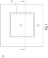
- FIG. 1 illustrates, in a simplified top-side-up plan view, an example die-in-die semiconductor device 100 in accordance with an embodiment.
- the semiconductor device 100 includes a first semiconductor die 102, a first cavity 106 formed in a backside of the first semiconductor die, and a second semiconductor die 104 mounted to the first semiconductor die within the cavity.
- each of the first semiconductor die 102 and the second semiconductor die 104 is arranged in an active-side-down orientation.
- the second semiconductor die 104 is interconnected through a bottom side of the first cavity 106 with one or more embedded conductive traces (not shown) of the back end of line (BEOL) region (not shown) of the first semiconductor die 102.
- BEOL back end of line
- conductive generally refers to electrical conductivity unless otherwise described.
- FIG. 2 illustrates, in a simplified cross-sectional view, the example die-in-die semiconductor device 100 at a stage of manufacture in accordance with an embodiment.
- the semiconductor device 100 includes the first semiconductor die 102.
- the first semiconductor die 102 has an active side (e.g., major side having circuitry, bond pads) and a backside (e.g., major side opposite of the active surface).
- the semiconductor die 102 is configured in a flip-chip (e.g., active-side-down) orientation.
- the BEOL region 202 and a front end of line (FEOL) region 204 are formed at the active side of the first semiconductor die 102.
- FEOL front end of line
- the FEOL region 204 generally includes the transistors process layers (e.g., gate, drain, source) and the BEOL region generally includes interconnection metal traces formed in subsequent process layers.
- a bulk region 206 generally includes the remaining bulk substrate portion of the first semiconductor die 102.
- the BEOL region 202 includes conductive features such as embedded interconnecting metal traces and vias 208, die interconnect traces 212, and connector pads 210 separated by dielectric material 214.
- the die interconnect traces 212 are configured to be exposed from the backside of the die and interconnected with the second semiconductor die 104 at subsequent stages of manufacture.
- the connector pads 210 are configured to be exposed at the active side of the die and have a plurality of conductive package connectors affixed at a subsequent stage of manufacture.
- the arrangement, location, and number of conductive features of the BEOL region 202 of the first semiconductor die 102 depicted in FIG. 2 are chosen for illustration purposes.
- the first semiconductor die 102 may be formed from any suitable semiconductor material, such as silicon, germanium, gallium arsenide, gallium nitride, and the like.
- the first semiconductor die 102 may further include digital circuits, analog circuits, RF circuits, power circuits, memory, processor, MEMS, sensor, the like, and combinations thereof integrated at the active side.
- FIG. 3 illustrates, in a simplified cross-sectional view, the example die-in-die semiconductor device 100 at a subsequent stage of manufacture in accordance with an embodiment.
- the semiconductor device 100 includes a first cavity 302 formed in the backside of the semiconductor die 102.
- the cavity 302 may be etched by way of one or more suitable etch processes, for example.
- the cavity 302 is formed to have predetermined width, length, and depth dimensions.
- the predetermined width, length, and depth dimensions of the cavity 302 are chosen to accommodate a second semiconductor die or other component to be mounted within the cavity at a subsequent stage of manufacture.
- a portion of the bulk region 206 remains between a bottom side of the cavity 302 and the FEOL region 204.
- the portion of the bulk region 206 remaining between the bottom of the cavity 302 and the FEOL region 204 may have a thickness approximately in a range of 30 to 50 microns.
- FIG. 4 illustrates, in a simplified cross-sectional view, the example die-in-die semiconductor device 100 at a subsequent stage of manufacture in accordance with an embodiment.
- the semiconductor device 100 includes a plurality of second cavities 402 formed in the backside of the semiconductor die 102.
- the second cavities 402 are formed beginning at the bottom side of the first cavity 303, extending vertically through the FEOL region 204, and ending at the embedded die interconnect traces 212 of the BEOL region 202.
- the plurality of cavities 402 may be etched by way of one or more suitable etch processes, for example.
- the embedded die interconnect traces 212 may serve as etch stops preventing the etch from progressing further into the BEOL region 202.
- Each cavity 402 is formed to have predetermined diameter and depth dimensions.
- the predetermined dimensions of the cavities 402 are chosen to accommodate respective die connectors (e.g., copper pillars, stud bumps) for interconnection of a second semiconductor die or other component mounted within the cavity at a subsequent stage of manufacture.
- FIG. 5 illustrates, in a simplified cross-sectional view, the example die-in-die semiconductor device 100 at a subsequent stage of manufacture in accordance with an embodiment.
- the semiconductor device 100 includes a thermal compression non-conductive paste (TCNCP) material 502 formed at the bottom side of the first cavity 302.
- TCNCP material 502 is dispensed into the first cavity 302 and second cavities 402.
- the dispensed TCNCP material 502 substantially fills the cavities 402 and covers the bottom surface of the cavity 302.
- the TCNCP material 502 remains uncured until after a second semiconductor die or other component is mounted within the cavity at a subsequent stage of manufacture.
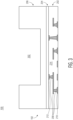
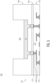
- FIG. 6 and FIG. 7 illustrate, in simplified cross-sectional views, the example die-in-die semiconductor device 100 at a subsequent stage of manufacture in accordance with an embodiment.
- the second semiconductor die 104 is positioned and aligned for mounting with the first cavity 302.
- the semiconductor die 104 includes bond pads 602 and respective copper pillars 604 affixed to the bond pads 602.
- the copper pillars 604 are formed with solder tips 606.
- the semiconductor die 104 with copper pillars 604 is inserted into the cavity 302 with a thermal compressive force such that the copper pillars 604 are pushed into respective cavities 402.
- the TCNCP material 502 is displaced allowing the tips (e.g., solder tips 606) of the copper pillars 604 to form conductive connections by engaging directly with the respective die interconnect traces 212 of the BEOL region 202 of the first semiconductor die 102.
- the active side of the semiconductor die 104 engages with the TCNCP material 502 and further displaces the TCNCP material 502 within the cavity 302.
- the TCNCP material 502 fills the gap formed between the active side of the semiconductor die 104 and the bottom of the cavity 302 and at least partially fills the gap formed between the sidewalls of the semiconductor die 104 and the sidewalls of the cavity 302.
- the TCNCP material 502 is subjected to a curing process. With the TCNCP material 502 cured, a hermetic seal is formed between the active side of the semiconductor die 104 and the bottom of the cavity 302 and between the sidewalls of the semiconductor die 104 and the sidewalls of the cavity 302.
- the backside of the second semiconductor die 104 is substantially coplanar with the backside of the first semiconductor die 102 after the semiconductor die 104 with copper pillars 604 is mounted in the cavity 302 and the TCNCP material 502 is cured.
- the backside of the second semiconductor die 104 may not be coplanar with the backside of the first semiconductor die 102 after the semiconductor die 104 with copper pillars 604 is mounted in the cavity 302 and the TCNCP material 502 is cured.
- FIG. 8 illustrates, in a simplified cross-sectional view, the example die-in-die semiconductor device 100 at a subsequent stage of manufacture in accordance with an embodiment.
- the semiconductor device 100 includes a plurality of conductive package connectors 802 affixed at the active side of the first semiconductor die 102.
- the conductive package connectors 802 are attached to respective package connector pads 210 exposed at the bottom side of the BEOL region 202 of the semiconductor die 102.
- the conductive connectors 802 are configured to provide a conductive connection between the first semiconductor die 102and a printed circuit board, for example.
- the conductive connectors 802 may be formed in suitable conductive connector structures such as solder balls, gold studs, copper pillars, and the like.
- the conductive connectors 802 are formed as ball connectors and arranged in a ball grid array.
- a method including forming a first cavity in a backside of a first semiconductor die, the first semiconductor die having a back end of line (BEOL) region, a front end of line (FEOL) region, and a bulk region; and mounting a second semiconductor die in the first cavity, a bond pad of the second semiconductor die interconnected through a bottom side of the first cavity with an embedded conductive trace of the BEOL region of the first semiconductor die.
- the method may further include forming a second cavity in the backside of the first semiconductor die, the second cavity beginning at the bottom side of the first cavity, extending vertically through the FEOL region, and ending at the embedded conductive trace of the BEOL region of the first semiconductor die.
- the mounting the second semiconductor die in the first cavity may further include inserting a copper pillar affixed to the bond pad of the second semiconductor into the second cavity to interconnect the bond pad with the embedded conductive trace of the BEOL region of the first semiconductor die.
- the method may further include dispensing a thermal compression non-conductive paste (TCNCP) material at the bottom side of the first cavity before mounting the second semiconductor die in the first cavity.
- TCNCP material may at least partially fill a gap region between sidewalls of the second semiconductor die and sidewalls of the first cavity after mounting the second semiconductor die in the first cavity.
- the second semiconductor die in the first cavity may further include applying a compressive force between the second semiconductor die and the first semiconductor die to interconnect the second semiconductor die with the embedded conductive trace of the BEOL region of the first semiconductor die.
- the forming the first cavity in the backside of the first semiconductor die may include forming the first cavity by way of a dry etch.
- a backside of the second semiconductor die and the backside of the first semiconductor die may be substantially coplanar after mounting the second semiconductor die in the first cavity.
- the method may further include affixing a plurality of conductive package connectors at an active side of the first semiconductor die.
- a semiconductor device including a first semiconductor die, the first semiconductor die having a back end of line (BEOL) region, a front end of line (FEOL) region, and a bulk region; a first cavity formed in a backside of the first semiconductor die; a second semiconductor die mounted in the first cavity, a bond pad of the second semiconductor die interconnected through a bottom side of the first cavity with an embedded conductive trace of the BEOL region of the first semiconductor die.
- the device may further include a second cavity formed in the backside of the first semiconductor die, the second cavity beginning at the bottom side of the first cavity, extending vertically through the FEOL region, and ending at the embedded conductive trace of the BEOL region of the first semiconductor die.
- the device may further include a copper pillar affixed to the bond pad of the second semiconductor and a solder-capped portion of the copper pillar affixed to the embedded conductive trace of the BEOL region of the first semiconductor die, the copper pillar at least partially disposed within the second cavity and configured to interconnect the bond pad with the embedded conductive trace.
- the device may further include a thermal compression non-conductive paste (TCNCP) material disposed in a gap between the bottom side of the first cavity and an active side of the second semiconductor, the TCNCP material configured to completely fill the gap.
- TCNCP thermal compression non-conductive paste
- a backside of the second semiconductor die and the backside of the first semiconductor die are substantially coplanar.
- the device may further include a plurality of conductive package connectors affixed at an active side of the first semiconductor die.
- a method including forming a first cavity in a backside of a first semiconductor die, the first semiconductor die having a back end of line (BEOL) region, a front end of line (FEOL) region, and a bulk region; and mounting a second semiconductor die in the first cavity, the second semiconductor die having a backside and an active side, a bond pad at the active side of the second semiconductor die interconnected through a bottom side of the first cavity with an embedded conductive trace of the BEOL region of the first semiconductor die.
- BEOL back end of line
- FEOL front end of line
- the method may further include forming a second cavity in the backside of the first semiconductor die, the second cavity beginning at the bottom side of the first cavity, extending vertically through the FEOL region, and ending at the embedded conductive trace of the BEOL region of the first semiconductor die.
- the mounting the second semiconductor die in the first cavity may further include inserting a copper pillar affixed to the bond pad of the second semiconductor into the second cavity to interconnect the bond pad with the embedded conductive trace of the BEOL region of the first semiconductor die.
- the method may further include dispensing a thermal compression non-conductive paste (TCNCP) material at the bottom side of the first cavity before mounting the second semiconductor die in the first cavity.
- TCNCP material may at least partially fill a gap region between sidewalls of the second semiconductor die and sidewalls of the first cavity after mounting the second semiconductor die in the first cavity.
- the die-in-die semiconductor device includes a first semiconductor die and a second semiconductor die interconnected with the first semiconductor through a backside of the first semiconductor die.
- a first cavity is formed in the backside of the first semiconductor die.
- the first cavity has width, length, and depth dimensions sufficient for mounting the second semiconductor die at least partially within the first cavity.
- a plurality of second cavities is formed in the backside of the first semiconductor die and begin at the bottom side of the first cavity, extend vertically through a front end of line region, and end at embedded die interconnect traces of a back end of line region. A portion of the die interconnect traces are exposed at the bottom of the second cavities.
- a thermal compression non-conductive paste material (e.g., commonly used in flip-chip packaging) is dispensed at the bottom side of the first cavity such that the second cavities are filled, and the bottom of the first cavity is covered.
- the second semiconductor die includes a plurality of copper pillar affixed to respective bond pads of the second semiconductor die.
- the second semiconductor die with copper pillars is inserted into the first cavity with a thermal compressive force such that the copper pillars are pushed into respective second cavities. With the copper pillars pushed into respective cavities, the thermal compression non-conductive paste material is displaced, and conductive connections are formed with the respective die interconnect traces of the first semiconductor die.
- a hermetic seal is formed in the first cavity between the second semiconductor die and the first semiconductor die.
Landscapes
- Wire Bonding (AREA)
- Engineering & Computer Science (AREA)
- Manufacturing & Machinery (AREA)
Abstract
A method of forming a die-in-die semiconductor device is provided. The method includes forming a first cavity in a backside of a first semiconductor die. The first semiconductor die has a back end of line (BEOL) region, a front end of line (FEOL) region, and a bulk region. A second semiconductor die is mounted in the first cavity. A bond pad of the second semiconductor die is interconnected through a bottom side of the first cavity with an embedded conductive trace of the BEOL region of the first semiconductor die.
Description
- This disclosure relates generally to semiconductor device packaging, and more specifically, to a die-in-die semiconductor device and method of forming the same.
- Today, there is an increasing trend to include sophisticated semiconductor devices in products and systems that are used every day. These sophisticated semiconductor devices may include features for specific applications which may impact the configuration of the semiconductor device packages, for example. With such features and applications, the configuration of the semiconductor device packages may limit performance of the semiconductor devices or impact the costs of the semiconductor devices. Accordingly, significant challenges exist in accommodating these features and applications while minimizing the impact on semiconductor devices' performance and costs.
- The present invention is illustrated by way of example and is not limited by the accompanying figures, in which like references indicate similar elements. Elements in the figures are illustrated for simplicity and clarity and have not necessarily been drawn to scale.
-
FIG. 1 illustrates, in a simplified top-side-up plan view, an example die-in-die semiconductor device at a stage of manufacture in accordance with an embodiment. -
FIG. 2 through FIG. 8 illustrate, in simplified cross-sectional views, the example die-in-die semiconductor device taken along line A-A ofFIG. 1 at various stages of manufacture in accordance with an embodiment. - Generally, there is provided, a die-in-die semiconductor device. The die-in-die semiconductor device includes a first semiconductor die and a second semiconductor die interconnected with the first semiconductor through a backside of the first semiconductor die. A first cavity is formed in the backside of the first semiconductor die. The first cavity has width, length, and depth dimensions sufficient for mounting the second semiconductor die at least partially within the first cavity. A plurality of second cavities is formed in the backside of the first semiconductor die and begin at the bottom side of the first cavity, extend vertically through a front end of line region, and end at embedded die interconnect traces of a back end of line region. A portion of the die interconnect traces are exposed at the bottom of the second cavities. After forming the second cavities, a thermal compression non-conductive paste material (e.g., commonly used in flip-chip packaging) is dispensed at the bottom side of the first cavity such that the second cavities are filled, and the bottom of the first cavity is covered. The second semiconductor die includes a plurality of copper pillar affixed to respective bond pads of the second semiconductor die. The second semiconductor die with copper pillars is inserted into the first cavity with a thermal compressive force such that the copper pillars are pushed into respective second cavities. With the copper pillars pushed into respective cavities, the thermal compression non-conductive paste material is displaced, and conductive connections are formed with the respective die interconnect traces of the first semiconductor die. With the thermal compression non-conductive paste material cured, a hermetic seal is formed in the first cavity between the second semiconductor die and the first semiconductor die. By forming the die-in-die semiconductor device in this manner, a compact interconnect, low-profile stacked die arrangement may be realized.
-
FIG. 1 illustrates, in a simplified top-side-up plan view, an example die-in-die semiconductor device 100 in accordance with an embodiment. At this stage, thesemiconductor device 100 includes afirst semiconductor die 102, a first cavity 106 formed in a backside of the first semiconductor die, and a second semiconductor die 104 mounted to the first semiconductor die within the cavity. As depicted inFIG. 1 , each of the first semiconductor die 102 and thesecond semiconductor die 104 is arranged in an active-side-down orientation. In this embodiment, thesecond semiconductor die 104 is interconnected through a bottom side of the first cavity 106 with one or more embedded conductive traces (not shown) of the back end of line (BEOL) region (not shown) of the first semiconductor die 102. The term "conductive," as used herein, generally refers to electrical conductivity unless otherwise described. By mounting and interconnecting the second semiconductor die 104 in this manner, a low-profile die-in-die stacked die arrangement may be realized, for example. With the second semiconductor die 104 mounted to the first semiconductor die 102, a gap separates sidewalls of the second semiconductor die 104 from sidewalls of the first cavity 106. The size, shape, and location of the first cavity 106 within the backside of thefirst semiconductor die 102 depicted inFIG. 1 are chosen for illustration purposes. Cross-sectional views of examples of the die-in-die semiconductor device 100 taken along line A-A ofFIG. 1 at various stages of manufacture are depicted inFIG. 2 through FIG. 8 . -
FIG. 2 illustrates, in a simplified cross-sectional view, the example die-in-die semiconductor device 100 at a stage of manufacture in accordance with an embodiment. At this stage, thesemiconductor device 100 includes the first semiconductor die 102. The first semiconductor die 102 has an active side (e.g., major side having circuitry, bond pads) and a backside (e.g., major side opposite of the active surface). In this embodiment, the semiconductor die 102 is configured in a flip-chip (e.g., active-side-down) orientation. The BEOLregion 202 and a front end of line (FEOL)region 204 are formed at the active side of the first semiconductor die 102. The FEOLregion 204 generally includes the transistors process layers (e.g., gate, drain, source) and the BEOL region generally includes interconnection metal traces formed in subsequent process layers. Abulk region 206 generally includes the remaining bulk substrate portion of the first semiconductor die 102. - In this embodiment, the BEOL
region 202 includes conductive features such as embedded interconnecting metal traces andvias 208, dieinterconnect traces 212, andconnector pads 210 separated bydielectric material 214. The dieinterconnect traces 212 are configured to be exposed from the backside of the die and interconnected with thesecond semiconductor die 104 at subsequent stages of manufacture. Theconnector pads 210 are configured to be exposed at the active side of the die and have a plurality of conductive package connectors affixed at a subsequent stage of manufacture. The arrangement, location, and number of conductive features of the BEOLregion 202 of the first semiconductor die 102 depicted inFIG. 2 are chosen for illustration purposes. - The first semiconductor die 102 may be formed from any suitable semiconductor material, such as silicon, germanium, gallium arsenide, gallium nitride, and the like. The first semiconductor die 102 may further include digital circuits, analog circuits, RF circuits, power circuits, memory, processor, MEMS, sensor, the like, and combinations thereof integrated at the active side.
-
FIG. 3 illustrates, in a simplified cross-sectional view, the example die-in-die semiconductor device 100 at a subsequent stage of manufacture in accordance with an embodiment. At this stage, thesemiconductor device 100 includes afirst cavity 302 formed in the backside of the semiconductor die 102. Thecavity 302 may be etched by way of one or more suitable etch processes, for example. Thecavity 302 is formed to have predetermined width, length, and depth dimensions. The predetermined width, length, and depth dimensions of thecavity 302 are chosen to accommodate a second semiconductor die or other component to be mounted within the cavity at a subsequent stage of manufacture. In this embodiment, a portion of thebulk region 206 remains between a bottom side of thecavity 302 and the FEOLregion 204. For example, after forming thecavity 302, the portion of thebulk region 206 remaining between the bottom of thecavity 302 and the FEOLregion 204 may have a thickness approximately in a range of 30 to 50 microns. -
FIG. 4 illustrates, in a simplified cross-sectional view, the example die-in-die semiconductor device 100 at a subsequent stage of manufacture in accordance with an embodiment. At this stage, thesemiconductor device 100 includes a plurality ofsecond cavities 402 formed in the backside of the semiconductor die 102. Thesecond cavities 402 are formed beginning at the bottom side of the first cavity 303, extending vertically through the FEOLregion 204, and ending at the embeddeddie interconnect traces 212 of theBEOL region 202. The plurality ofcavities 402 may be etched by way of one or more suitable etch processes, for example. In some embodiments, the embeddeddie interconnect traces 212 may serve as etch stops preventing the etch from progressing further into the BEOLregion 202. As a result of forming thecavities 402, portions of the embeddeddie interconnect traces 212 are exposed from the backside of the semiconductor die 102. Eachcavity 402 is formed to have predetermined diameter and depth dimensions. The predetermined dimensions of thecavities 402 are chosen to accommodate respective die connectors (e.g., copper pillars, stud bumps) for interconnection of a second semiconductor die or other component mounted within the cavity at a subsequent stage of manufacture. -
FIG. 5 illustrates, in a simplified cross-sectional view, the example die-in-die semiconductor device 100 at a subsequent stage of manufacture in accordance with an embodiment. At this stage, thesemiconductor device 100 includes a thermal compression non-conductive paste (TCNCP)material 502 formed at the bottom side of thefirst cavity 302. In this embodiment, theTCNCP material 502 is dispensed into thefirst cavity 302 andsecond cavities 402. The dispensedTCNCP material 502 substantially fills thecavities 402 and covers the bottom surface of thecavity 302. In this embodiment, theTCNCP material 502 remains uncured until after a second semiconductor die or other component is mounted within the cavity at a subsequent stage of manufacture. -
FIG. 6 andFIG. 7 illustrate, in simplified cross-sectional views, the example die-in-die semiconductor device 100 at a subsequent stage of manufacture in accordance with an embodiment. As depicted inFIG. 6 , the second semiconductor die 104 is positioned and aligned for mounting with thefirst cavity 302. In this embodiment, the semiconductor die 104 includesbond pads 602 andrespective copper pillars 604 affixed to thebond pads 602. In this embodiment, thecopper pillars 604 are formed withsolder tips 606. As depicted by the arrows ofFIG. 6 , the semiconductor die 104 withcopper pillars 604 is inserted into thecavity 302 with a thermal compressive force such that thecopper pillars 604 are pushed intorespective cavities 402. With thecopper pillars 604 pushed intorespective cavities 402 as depicted inFIG. 7 , theTCNCP material 502 is displaced allowing the tips (e.g., solder tips 606) of thecopper pillars 604 to form conductive connections by engaging directly with the respective die interconnect traces 212 of theBEOL region 202 of the first semiconductor die 102. - Concurrently, as the semiconductor die 104 with
copper pillars 604 is inserted into thecavity 302 with the thermal compressive force, the active side of the semiconductor die 104 engages with theTCNCP material 502 and further displaces theTCNCP material 502 within thecavity 302. With theTCNCP material 502 further displaced by the inserted semiconductor die 104 withcopper pillars 604, theTCNCP material 502 fills the gap formed between the active side of the semiconductor die 104 and the bottom of thecavity 302 and at least partially fills the gap formed between the sidewalls of the semiconductor die 104 and the sidewalls of thecavity 302. - After the semiconductor die 104 with
copper pillars 604 is mounted in thecavity 302 and the conductive connections are formed between thecopper pillars 604 and respective die interconnect traces 212, theTCNCP material 502 is subjected to a curing process. With theTCNCP material 502 cured, a hermetic seal is formed between the active side of the semiconductor die 104 and the bottom of thecavity 302 and between the sidewalls of the semiconductor die 104 and the sidewalls of thecavity 302. In this embodiment, the backside of the second semiconductor die 104 is substantially coplanar with the backside of the first semiconductor die 102 after the semiconductor die 104 withcopper pillars 604 is mounted in thecavity 302 and theTCNCP material 502 is cured. In some embodiments, the backside of the second semiconductor die 104 may not be coplanar with the backside of the first semiconductor die 102 after the semiconductor die 104 withcopper pillars 604 is mounted in thecavity 302 and theTCNCP material 502 is cured. -
FIG. 8 illustrates, in a simplified cross-sectional view, the example die-in-die semiconductor device 100 at a subsequent stage of manufacture in accordance with an embodiment. At this stage, thesemiconductor device 100 includes a plurality ofconductive package connectors 802 affixed at the active side of the first semiconductor die 102. In this embodiment, theconductive package connectors 802 are attached to respectivepackage connector pads 210 exposed at the bottom side of theBEOL region 202 of the semiconductor die 102. Theconductive connectors 802 are configured to provide a conductive connection between the first semiconductor die 102and a printed circuit board, for example. Theconductive connectors 802 may be formed in suitable conductive connector structures such as solder balls, gold studs, copper pillars, and the like. For illustration purposes, theconductive connectors 802 are formed as ball connectors and arranged in a ball grid array. - Generally, there is provided, a method including forming a first cavity in a backside of a first semiconductor die, the first semiconductor die having a back end of line (BEOL) region, a front end of line (FEOL) region, and a bulk region; and mounting a second semiconductor die in the first cavity, a bond pad of the second semiconductor die interconnected through a bottom side of the first cavity with an embedded conductive trace of the BEOL region of the first semiconductor die. The method may further include forming a second cavity in the backside of the first semiconductor die, the second cavity beginning at the bottom side of the first cavity, extending vertically through the FEOL region, and ending at the embedded conductive trace of the BEOL region of the first semiconductor die. The mounting the second semiconductor die in the first cavity may further include inserting a copper pillar affixed to the bond pad of the second semiconductor into the second cavity to interconnect the bond pad with the embedded conductive trace of the BEOL region of the first semiconductor die. The method may further include dispensing a thermal compression non-conductive paste (TCNCP) material at the bottom side of the first cavity before mounting the second semiconductor die in the first cavity. The TCNCP material may at least partially fill a gap region between sidewalls of the second semiconductor die and sidewalls of the first cavity after mounting the second semiconductor die in the first cavity. The second semiconductor die in the first cavity may further include applying a compressive force between the second semiconductor die and the first semiconductor die to interconnect the second semiconductor die with the embedded conductive trace of the BEOL region of the first semiconductor die. The forming the first cavity in the backside of the first semiconductor die may include forming the first cavity by way of a dry etch. A backside of the second semiconductor die and the backside of the first semiconductor die may be substantially coplanar after mounting the second semiconductor die in the first cavity. The method may further include affixing a plurality of conductive package connectors at an active side of the first semiconductor die.
- In another embodiment, there is provided, a semiconductor device including a first semiconductor die, the first semiconductor die having a back end of line (BEOL) region, a front end of line (FEOL) region, and a bulk region; a first cavity formed in a backside of the first semiconductor die; a second semiconductor die mounted in the first cavity, a bond pad of the second semiconductor die interconnected through a bottom side of the first cavity with an embedded conductive trace of the BEOL region of the first semiconductor die. The device may further include a second cavity formed in the backside of the first semiconductor die, the second cavity beginning at the bottom side of the first cavity, extending vertically through the FEOL region, and ending at the embedded conductive trace of the BEOL region of the first semiconductor die. The device may further include a copper pillar affixed to the bond pad of the second semiconductor and a solder-capped portion of the copper pillar affixed to the embedded conductive trace of the BEOL region of the first semiconductor die, the copper pillar at least partially disposed within the second cavity and configured to interconnect the bond pad with the embedded conductive trace. The device may further include a thermal compression non-conductive paste (TCNCP) material disposed in a gap between the bottom side of the first cavity and an active side of the second semiconductor, the TCNCP material configured to completely fill the gap. A backside of the second semiconductor die and the backside of the first semiconductor die are substantially coplanar. The device may further include a plurality of conductive package connectors affixed at an active side of the first semiconductor die.
- In yet another embodiment, there is provided, a method including forming a first cavity in a backside of a first semiconductor die, the first semiconductor die having a back end of line (BEOL) region, a front end of line (FEOL) region, and a bulk region; and mounting a second semiconductor die in the first cavity, the second semiconductor die having a backside and an active side, a bond pad at the active side of the second semiconductor die interconnected through a bottom side of the first cavity with an embedded conductive trace of the BEOL region of the first semiconductor die. The method may further include forming a second cavity in the backside of the first semiconductor die, the second cavity beginning at the bottom side of the first cavity, extending vertically through the FEOL region, and ending at the embedded conductive trace of the BEOL region of the first semiconductor die. The mounting the second semiconductor die in the first cavity may further include inserting a copper pillar affixed to the bond pad of the second semiconductor into the second cavity to interconnect the bond pad with the embedded conductive trace of the BEOL region of the first semiconductor die. The method may further include dispensing a thermal compression non-conductive paste (TCNCP) material at the bottom side of the first cavity before mounting the second semiconductor die in the first cavity. The TCNCP material may at least partially fill a gap region between sidewalls of the second semiconductor die and sidewalls of the first cavity after mounting the second semiconductor die in the first cavity.
- By now, it should be appreciated that there has been provided a die-in-die semiconductor device. The die-in-die semiconductor device includes a first semiconductor die and a second semiconductor die interconnected with the first semiconductor through a backside of the first semiconductor die. A first cavity is formed in the backside of the first semiconductor die. The first cavity has width, length, and depth dimensions sufficient for mounting the second semiconductor die at least partially within the first cavity. A plurality of second cavities is formed in the backside of the first semiconductor die and begin at the bottom side of the first cavity, extend vertically through a front end of line region, and end at embedded die interconnect traces of a back end of line region. A portion of the die interconnect traces are exposed at the bottom of the second cavities. After forming the second cavities, a thermal compression non-conductive paste material (e.g., commonly used in flip-chip packaging) is dispensed at the bottom side of the first cavity such that the second cavities are filled, and the bottom of the first cavity is covered. The second semiconductor die includes a plurality of copper pillar affixed to respective bond pads of the second semiconductor die. The second semiconductor die with copper pillars is inserted into the first cavity with a thermal compressive force such that the copper pillars are pushed into respective second cavities. With the copper pillars pushed into respective cavities, the thermal compression non-conductive paste material is displaced, and conductive connections are formed with the respective die interconnect traces of the first semiconductor die. With the thermal compression non-conductive paste material cured, a hermetic seal is formed in the first cavity between the second semiconductor die and the first semiconductor die. By forming the die-in-die semiconductor device in this manner, a compact interconnect, low-profile stacked die arrangement may be realized.
- The terms "front," "back," "top," "bottom," "over," "under" and the like in the description and in the claims, if any, are used for descriptive purposes and not necessarily for describing permanent relative positions. It is understood that the terms so used are interchangeable under appropriate circumstances such that the embodiments of the invention described herein are, for example, capable of operation in other orientations than those illustrated or otherwise described herein.
- Although the invention is described herein with reference to specific embodiments, various modifications and changes can be made without departing from the scope of the present invention as set forth in the claims below. Accordingly, the specification and figures are to be regarded in an illustrative rather than a restrictive sense, and all such modifications are intended to be included within the scope of the present invention. Any benefits, advantages, or solutions to problems that are described herein with regard to specific embodiments are not intended to be construed as a critical, required, or essential feature or element of any or all the claims.
- Furthermore, the terms "a" or "an," as used herein, are defined as one or more than one. Also, the use of introductory phrases such as "at least one" and "one or more" in the claims should not be construed to imply that the introduction of another claim element by the indefinite articles "a" or "an" limits any particular claim containing such introduced claim element to inventions containing only one such element, even when the same claim includes the introductory phrases "one or more" or "at least one" and indefinite articles such as "a" or "an." The same holds true for the use of definite articles.
- Unless stated otherwise, terms such as "first" and "second" are used to arbitrarily distinguish between the elements such terms describe. Thus, these terms are not necessarily intended to indicate temporal or other prioritization of such elements.
Claims (14)
- A method comprising:forming a first cavity in a backside of a first semiconductor die, the first semiconductor die having a back end of line, BEOL, region, a front end of line, FEOL, region, and a bulk region; andmounting a second semiconductor die in the first cavity, a bond pad of the second semiconductor die interconnected through a bottom side of the first cavity with an embedded conductive trace of the BEOL region of the first semiconductor die.
- The method of claim 1, further comprising forming a second cavity in the backside of the first semiconductor die, the second cavity beginning at the bottom side of the first cavity, extending vertically through the FEOL region, and ending at the embedded conductive trace of the BEOL region of the first semiconductor die.
- The method of claim 2, wherein mounting the second semiconductor die in the first cavity further comprises inserting a copper pillar affixed to the bond pad of the second semiconductor into the second cavity to interconnect the bond pad with the embedded conductive trace of the BEOL region of the first semiconductor die.
- The method of claim 1, further comprising dispensing a thermal compression non-conductive paste, TCNCP, material at the bottom side of the first cavity before mounting the second semiconductor die in the first cavity.
- The method of claim 4, wherein the TCNCP material at least partially fills a gap region between sidewalls of the second semiconductor die and sidewalls of the first cavity after mounting the second semiconductor die in the first cavity.
- The method of claim 1, wherein mounting the second semiconductor die in the first cavity further comprises applying a compressive force between the second semiconductor die and the first semiconductor die to interconnect the the second semiconductor die with the embedded conductive trace of the BEOL region of the first semiconductor die.
- The method of claim 1, wherein forming the first cavity in the backside of the first semiconductor die includes forming the first cavity by way of a dry etch.
- The method of claim 1, wherein a backside of the second semiconductor die and the backside of the first semiconductor die are substantially coplanar after mounting the second semiconductor die in the first cavity.
- The method of claim 1, further comprising affixing a plurality of conductive package connectors at an active side of the first semiconductor die.
- A method comprising:forming a first cavity in a backside of a first semiconductor die, the first semiconductor die having a back end of line, BEOL, region, a front end of line, FEOL, region, and a bulk region; andmounting a second semiconductor die in the first cavity, the second semiconductor die having a backside and an active side, a bond pad at the active side of the second semiconductor die interconnected through a bottom side of the first cavity with an embedded conductive trace of the BEOL region of the first semiconductor die.
- The method of claim 10, further comprising forming a second cavity in the backside of the first semiconductor die, the second cavity beginning at the bottom side of the first cavity, extending vertically through the FEOL region, and ending at the embedded conductive trace of the BEOL region of the first semiconductor die.
- The method of claim 11, wherein mounting the second semiconductor die in the first cavity further comprises inserting a copper pillar affixed to the bond pad of the second semiconductor into the second cavity to interconnect the bond pad with the embedded conductive trace of the BEOL region of the first semiconductor die.
- The method of any of claims 10 to 12, further comprising dispensing a thermal compression non-conductive paste, TCNCP, material at the bottom side of the first cavity before mounting the second semiconductor die in the first cavity.
- The method of claim 13, wherein the TCNCP material at least partially fills a gap region between sidewalls of the second semiconductor die and sidewalls of the first cavity after mounting the second semiconductor die in the first cavity.
Applications Claiming Priority (1)
| Application Number | Priority Date | Filing Date | Title |
|---|---|---|---|
| US18/505,364 US20250157986A1 (en) | 2023-11-09 | 2023-11-09 | Die in die semiconductor device and method therefor |
Publications (1)
| Publication Number | Publication Date |
|---|---|
| EP4553899A1 true EP4553899A1 (en) | 2025-05-14 |
Family
ID=93460678
Family Applications (1)
| Application Number | Title | Priority Date | Filing Date |
|---|---|---|---|
| EP24211867.7A Pending EP4553899A1 (en) | 2023-11-09 | 2024-11-08 | Die in die semiconductor device and method therefor |
Country Status (2)
| Country | Link |
|---|---|
| US (1) | US20250157986A1 (en) |
| EP (1) | EP4553899A1 (en) |
Citations (2)
| Publication number | Priority date | Publication date | Assignee | Title |
|---|---|---|---|---|
| WO2012011929A1 (en) * | 2010-07-23 | 2012-01-26 | Tessera, Inc. | Active chip on carrier or laminated chip having microelectronic element embedded therein |
| KR20140042226A (en) * | 2012-09-28 | 2014-04-07 | 에스케이하이닉스 주식회사 | Semiconductor chip and stack package using the same |
Family Cites Families (1)
| Publication number | Priority date | Publication date | Assignee | Title |
|---|---|---|---|---|
| US9799590B2 (en) * | 2013-03-13 | 2017-10-24 | STATS ChipPAC Pte. Ltd. | Semiconductor device and method of using partial wafer singulation for improved wafer level embedded system in package |
-
2023
- 2023-11-09 US US18/505,364 patent/US20250157986A1/en active Pending
-
2024
- 2024-11-08 EP EP24211867.7A patent/EP4553899A1/en active Pending
Patent Citations (2)
| Publication number | Priority date | Publication date | Assignee | Title |
|---|---|---|---|---|
| WO2012011929A1 (en) * | 2010-07-23 | 2012-01-26 | Tessera, Inc. | Active chip on carrier or laminated chip having microelectronic element embedded therein |
| KR20140042226A (en) * | 2012-09-28 | 2014-04-07 | 에스케이하이닉스 주식회사 | Semiconductor chip and stack package using the same |
Also Published As
| Publication number | Publication date |
|---|---|
| US20250157986A1 (en) | 2025-05-15 |
Similar Documents
| Publication | Publication Date | Title |
|---|---|---|
| JP6408986B2 (en) | BVA interposer | |
| US8154134B2 (en) | Packaged electronic devices with face-up die having TSV connection to leads and die pad | |
| US6081997A (en) | System and method for packaging an integrated circuit using encapsulant injection | |
| US8039943B2 (en) | Semiconductor device and manufacturing method therefor | |
| US20110215438A1 (en) | Stacked Semiconductor Package Having Discrete Components | |
| WO2015039043A2 (en) | Microelectronic element with bond elements to encapsulation surface | |
| CN112310063A (en) | Semiconductor device package and method of manufacturing the same | |
| KR20050077866A (en) | Semiconductor package with heat-dissipating structure and method for fabricating the same | |
| KR20050037430A (en) | Semiconductor package device and method of formation and testing | |
| JP2008244451A (en) | Semiconductor device package with die receiving through-hole and through-hole connecting structure and method of the same | |
| US12387985B2 (en) | Semiconductor device with cavity carrier and method therefor | |
| CN101006570A (en) | Land grid array packaged device and method of forming same | |
| KR20110130365A (en) | Integrated circuit packaging system with double side connections and manufacturing method thereof | |
| US7190066B2 (en) | Heat spreader and package structure utilizing the same | |
| CN111128920A (en) | Semiconductor device and manufacturing method thereof | |
| EP4632809A1 (en) | Semiconductor device with embedded flex substrate and method therefor | |
| US6879050B2 (en) | Packaged microelectronic devices and methods for packaging microelectronic devices | |
| US20250157986A1 (en) | Die in die semiconductor device and method therefor | |
| EP4456126B1 (en) | Semiconductor device with rigid-flex sub-assembly and method therefor | |
| US8481366B2 (en) | Semiconductor device and manufacturing method therefor | |
| US7732934B2 (en) | Semiconductor device having conductive adhesive layer and method of fabricating the same | |
| US12388030B2 (en) | Semiconductor device with stress relief feature and method therefor | |
| US20080006940A1 (en) | Lead frames, microelectronic devices with lead frames, and methods for manufacturing lead frames and microelectronic devices with lead frames | |
| JP2002176069A (en) | Structure of electrical connection terminal and manufacturing method thereof | |
| EP4708360A1 (en) | Semiconductor device with interposer and method therefor |
Legal Events
| Date | Code | Title | Description |
|---|---|---|---|
| PUAI | Public reference made under article 153(3) epc to a published international application that has entered the european phase |
Free format text: ORIGINAL CODE: 0009012 |
|
| STAA | Information on the status of an ep patent application or granted ep patent |
Free format text: STATUS: THE APPLICATION HAS BEEN PUBLISHED |
|
| AK | Designated contracting states |
Kind code of ref document: A1 Designated state(s): AL AT BE BG CH CY CZ DE DK EE ES FI FR GB GR HR HU IE IS IT LI LT LU LV MC ME MK MT NL NO PL PT RO RS SE SI SK SM TR |
|
| STAA | Information on the status of an ep patent application or granted ep patent |
Free format text: STATUS: REQUEST FOR EXAMINATION WAS MADE |
|
| 17P | Request for examination filed |
Effective date: 20251114 |