EP4550567A1 - Waveguide converter, package for mounting electronic component, and waveguide conversion device - Google Patents
Waveguide converter, package for mounting electronic component, and waveguide conversion device Download PDFInfo
- Publication number
- EP4550567A1 EP4550567A1 EP23831492.6A EP23831492A EP4550567A1 EP 4550567 A1 EP4550567 A1 EP 4550567A1 EP 23831492 A EP23831492 A EP 23831492A EP 4550567 A1 EP4550567 A1 EP 4550567A1
- Authority
- EP
- European Patent Office
- Prior art keywords
- region
- planar view
- waveguide converter
- frame
- waveguide
- Prior art date
- Legal status (The legal status is an assumption and is not a legal conclusion. Google has not performed a legal analysis and makes no representation as to the accuracy of the status listed.)
- Withdrawn
Links
Images








Classifications
-
- H—ELECTRICITY
- H01—ELECTRIC ELEMENTS
- H01P—WAVEGUIDES; RESONATORS, LINES, OR OTHER DEVICES OF THE WAVEGUIDE TYPE
- H01P5/00—Coupling devices of the waveguide type
- H01P5/08—Coupling devices of the waveguide type for linking dissimilar lines or devices
- H01P5/10—Coupling devices of the waveguide type for linking dissimilar lines or devices for coupling balanced lines or devices with unbalanced lines or devices
- H01P5/107—Hollow-waveguide/strip-line transitions
Definitions
- the present disclosure relates to a waveguide converter, an electronic component mounting package, and a waveguide conversion device.
- Wireless communication has been adopting a higher frequency band along with requests for increases in speed and volume of the wireless communication. Accordingly, signals to be processed by wireless devices have also been adopting higher frequencies.
- Examples of a transmission medium configured to efficiently transmit such a radio-frequency signal include a waveguide.
- a waveguide cannot be connected directly to an integrated circuit mounted on a circuit board. Therefore widely adopted is a configuration in which the integrated circuit and the waveguide interpose a microstrip line. Adopting such a configuration needs a converter configured to mutually convert a signal between the waveguide and the microstrip line.
- Patent Literature 1 describes a known invention relating to such a converter.
- a converter includes a waveguide-planar line conversion substrate including a dielectric substrate provided with a ground layer and a signal line configured to propagate a radio-frequency signal, and a housing including a waveguide.
- the waveguide-planar line conversion substrate includes an upper surface provided with a short lid (see FIG. 1 and the like of Patent Literature 1).
- Patent Literature 1 Japanese Unexamined Patent Application Publication No. 2004-96206
- a waveguide converter (1) includes a first substrate, a signal conductor, a first ground conductor, a first frame, a second ground conductor, and a first lid.
- the first substrate includes a first upper surface including a first region and a second region extending from the first region.
- the signal conductor includes a conversion portion positioned in the first region, and a line portion connected to the conversion portion and positioned to extend at least from the first region to the second region.
- the first ground conductor is positioned to interpose the line portion at least in the second region on the first upper surface in a plannar view.
- the first frame includes a second upper surface and an inner surface connected to the second upper surface.
- the first frame is positioned on the first upper surface to surround at least part of the first region and the second region in a planar view.
- the first frame is made of a nonmetallic material.
- the second ground conductor is positioned on the second upper surface.
- the first lid is positioned on the second upper surface to cover the first region in a planar view.
- the first lid is made of a metallic material.
- the first frame further includes a first end portion and a second end portion positioned to face each other and interpose the second region in a planar view. The first ground conductor, the second ground conductor, and the first lid are electrically connected to one another.
- a waveguide converter may be disposed to include a top or a bottom in any direction.
- the waveguide converter is defined to have an orthogonal coordinate system xyz, and a positive side in a z direction is assumed to indicate an upper side.
- the present disclosure refers to a first direction exemplarily indicating an x direction in the drawings.
- a second direction crossing the first direction exemplarily indicates a y direction in the drawings.
- the present disclosure refers to an outward direction exemplarily indicating a direction away from a first region 1a1 to be described later in the x direction or the y direction.
- the present disclosure refers to a planar view as a concept inclusive of a plan perspective view.
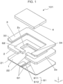
- the waveguide converter 101 includes a first substrate 1, a signal conductor S1, a first ground conductor G1, a first frame 2, a second ground conductor G2, and a first lid 4.
- the first substrate 1 includes a first upper surface 1a including the first region 1a1 and a second region 1a2 extending from the first region 1a1.
- the first substrate 1 is made of a nonmetallic material or the like.
- the material for the first substrate 1 can include nonmetallic materials including a ceramic material such as an aluminum oxide sintered body, a mullite sintered body, a silicon carbide sintered body, an aluminum nitride sintered body, or a silicon nitride sintered body, and a glass ceramic material.
- the first substrate 1 may alternatively be constituted by a printed circuit board such as a copper-clad laminate.
- the first substrate 1 may be constituted by a single layer made of a nonmetallic material or a multilayered product made of a nonmetallic material.
- the first substrate 1 exemplarily has a rectangular shape in a planar view having 4 mm ⁇ 4 mm to 50 mm ⁇ 50 mm in size and 0.05 mm to 1 mm in thickness.
- the first substrate 1 may include a single or a plurality of via holes.
- the via hole can be formed by providing the first substrate 1 with a bore having an outer shape of the via hole and filling the bore with a conductive paste containing refractory metal powder of tungsten, molybdenum, or the like.
- the first substrate 1 further includes a first lower surface 1b.
- the first lower surface 1b may be provided with a third ground conductor G3.
- the third ground conductor G3 may be an annular metal layer positioned to surround the first region 1a1 in a planar view.
- the third ground conductor G3 may be electrically connected to the first ground conductor G1 to be described later by mean of the via hole or the like.
- the third ground conductor G3 positioned on the first lower surface 1b can enhance ground potential of the signal conductor S1, as well as can serve as a conductive wall electromagnetically connected to a waveguide 107 to be described later.
- the first frame 2 includes a second upper surface 2a and an inner surface 2c connected to the second upper surface 2a.
- the first frame 2 is positioned on the first upper surface 1a to surround at least part of the first region 1a1 and the second region 1a2 in a planar view.
- the first frame 2 further includes a first end portion 21 and a second end portion 22 positioned to face each other and interpose the second region 1a2 in a planar view.
- the first frame 2 is made of a nonmetallic material.
- the material for the first frame 2 may be the same as or different from the material for the first substrate 1, and examples of the material for the first frame 2 include materials the same as or similar to the examples of the material for the first substrate 1.
- the first substrate 1 and the first frame 2 are each made of a ceramic material or a glass ceramic material
- the first substrate 1 and the first frame 2 can be manufactured by stacking green sheets formed into outer shapes of the first substrate 1 and the first frame 2. This can facilitate manufacture of the waveguide converter 101.
- the first frame 2 exemplarily has a U shape in a planar view having 4 mm ⁇ 4 mm to 50 mm ⁇ 50 mm in size and 0.1 mm to 5 mm in thickness.
- the first frame 2 may alternatively be provided with a via hole in the same or a similar manner to the first substrate 1. Provision of the via hole can facilitate electrical connection of the first ground conductor G1 to be described later, the second ground conductor G2, and the first lid 4.
- the via hole can be formed in the same or a similar manner to the via hole provided in the first substrate 1.
- the signal conductor S1 includes a conversion portion S11 positioned in the first region 1a1, and a line portion S12 connected to the conversion portion S11 and positioned to extend at least from the first region 1a1 to the second region 1a2.
- the signal conductor S1 is made of a material, examples of which include metallic materials such as gold, silver, copper, nickel, tungsten, molybdenum, and manganese.
- the signal conductor S1 may be formed by sintering a metal paste on the first upper surface 1a of the first substrate 1, or may be formed by applying a thin film forming technique such as an evaporation method or a sputtering method.
- the signal conductor S1 may be electrically connected to an electronic component 104 to be described later via a connector such as a wire principally made of a conductive metallic material such as platinum.
- Examples of the signal conductor S1 include a transmission line configured suitably for transmission of a radio-frequency signal such as a millimeter wave.
- a signal transmitted through the line portion S12 is electromagnetically coupled to the waveguide 107 to be described later in the conversion portion S11.
- the first ground conductor G1 is positioned to interpose the line portion S12 at least in the second region 1a2 on the first upper surface 1a in a planar view.
- the first ground conductor G1 is made of a material that may be the same as or different from the material for the signal conductor S1, and examples of the material for the first ground conductor G1 include materials the same as or similar to the examples of the material for the signal conductor S1.
- the first ground conductor G1 may be formed in the same or a similar manner to the signal conductor S1.
- the signal conductor S1 and the first ground conductor G1 are positioned also in a third region 1a3 to be described later, and the first ground conductor G1 is positioned to interpose the line portion S12 in a planar view also in the third region 1a3.
- the signal conductor S1 is positioned to be interposed by the first ground conductor G1 to enhance ground potential and strengthen electric field coupling. This is less likely to cause a resonance generated by an electric field distribution expanding beyond a desired range when a radio-frequency signal is transmitted through the signal conductor S1.
- the first ground conductor G1 is not necessarily positioned to interpose the line portion S12 in a planar view in the third region 1a3.
- the first ground conductor G1 may include a pair of metal films separately provided on the first upper surface 1a so as to be positioned to interpose the signal conductor S1.
- the first ground conductor G1 may be electrically connected to the electronic component 104 to be described later via a connector such as a wire.
- the second ground conductor G2 is positioned on the second upper surface 2a.
- the second ground conductor G2 is made of a material that may be the same as or different from the material for the signal conductor S1, and examples of the material for the second ground conductor G2 include materials the same as or similar to the examples of the material for the signal conductor S1.
- the second ground conductor G2 may be formed in the same or a similar manner to the signal conductor S1. Provision of the second ground conductor G2 facilitates bonding the first lid 4 to be described later to the first frame 2.
- the second ground conductor G2 is positioned continuously from the second upper surface 2a to the inner surface 2c of the first frame 2 as illustrated in FIG. 1 .
- the second ground conductor G2 may be positioned continuously to a surface opposite to the second upper surface 2a of the first frame 2 (a surface facing the first upper surface 1a). This facilitates electrical connection of the first ground conductor G1, the second ground conductor G2, and the first lid 4.
- ground potential can be enhanced to reduce a signal loss generated when a radio-frequency signal is transmitted through the signal conductor S1.
- the second ground conductor G2 is electrically connected to the first lid 4 to be described later so as to be regarded as a so-called dummy back-short block (in other words, conductor block).
- the first frame 2 and the first lid 4 can be regarded as an integral lid.
- the first lid 4 is positioned on the second upper surface 2a to cover the first region 1a1 in a planar view.
- the first lid 4 is made of a metallic material.
- the first lid 4 exemplarily has a quadrilateral shape in a planar view having 1 mm ⁇ 1 mm to 50 mm ⁇ 50 mm in size and 0.2 mm to 20 mm in thickness.
- Examples of the material for the first lid 4 include metallic materials such as iron, copper, nickel, chrome, cobalt, molybdenum, and tungsten, and an alloy obtained by combining some of these metallic materials.
- a metal member constituting the first lid 4 can be manufactured by applying a metalworking method such as a metal rolling method or a punching method to an ingot made of such a metallic material.
- the first lid 4 allows a signal transmitted through the signal conductor S1 to efficiently enter the waveguide 107.
- the first lid 4 further allows a signal having propagated through the waveguide 107 to efficiently enter the signal conductor S1.
- the first lid 4 can be bonded to the first frame 2 and the second ground conductor G2 by a bonding material.
- the first ground conductor G1, the second ground conductor G2, and the first lid 4 are electrically connected to one another.
- the first ground conductor G1, the second ground conductor G2, and the first lid 4 are electrically connected by the first ground conductor G2 positioned to extend to the via hole and the inner surface 2c of the first frame 2. This can enhance ground potential.
- the present disclosure is not limited to the above embodiment as long as the first ground conductor G1, the second ground conductor G2, and the first lid 4 can be electrically connected to one another.
- the waveguide converter 101 may further include a second frame 3 made of a nonmetallic material.
- the second frame 3 is positioned on the second upper surface 2a to surround at least part of the first region 1a1 outside the inner surface 2c in a planar view.
- the second frame 3 further includes a third end portion 33 and a fourth end portion 34 positioned to face each other in the y direction in a planar view.
- the material for the second frame 3 may be the same as or different from the material for the first frame 2, and examples of the material for the second frame 3 include materials the same as or similar to the examples of the material for the first frame 2.
- the first substrate 1, the first frame 2, and the second frame 3 are each made of a ceramic material or a glass ceramic material
- the first substrate 1, the first frame 2, and the second frame 3 can be manufactured by stacking green sheets formed into outer shapes of the first substrate 1, the first frame 2, and the second frame 3. This can facilitate manufacture of the waveguide converter 101.
- the second frame 3 exemplarily has a U shape in a planar view having 4 mm ⁇ 4 mm to 50 mm ⁇ 50 mm in size and 0.1 mm to 5 mm in thickness.
- the second frame 3 having the U shape is less likely to warp upon sintering.
- the second frame 3 is not limitedly to have the U shape as long as the second frame 3 can serve as the positioning guide upon bonding the first lid 4.
- the second frame 3 may alternatively have an L shape, a shape obtained by halving and separating the U shape, or the like.
- the second frame 3 is positioned on the second upper surface 2a to surround at least part of the first region 1a1 outside the inner surface 2c in a planar view. More specifically, the second frame 3 includes an inner edge positioned outside an inner edge of the first frame 2 in a planar view. In an embodiment, each of three sides of the inner edge of the second frame 3 and a corresponding one of three sides of the inner edge of the first frame 2 have a constant distance in a planar view.
- the second frame 3 includes an outer edge matching outer edges of the first substrate 1 and the first frame 2 in a planar view.
- the outer edge of the second frame 3 does not necessarily match the outer edges of the first substrate 1 and the first frame 2. That is, the outer edge of the second frame 3 may be larger or smaller than the outer edges of the first substrate 1 and the first frame 2.
- a size in the x direction of a portion of the first frame opposite to a portion positioned to surround the second region 1a2 so as to interpose the first region 1a1 is Lx23, (Lx21 + Lx22) > Lx23 may be satisfied.
- the second frame 3 can thus be positioned stably on the first frame 2 in this configuration.
- a distance L12 ( FIG. 8 ) in the y direction between the first end portion 21 and the second end portion 22 of the first frame 2 may be equal to or less than a distance L34 ( FIG. 9 ) in the y direction between the third end portion 33 and the fourth end portion 34 of the second frame 3.
- Such a configuration allows the first lid 4 to be fitted from an opened side (a portion interposed between the third end portion 33 and the fourth end portion 34) of the second frame 3 upon bonding the first lid 4 to the first frame 2. This can facilitate manufacture of the waveguide converter 101.
- the first lid 4 may include a first surface 411 positioned to face the first region 1a1.
- a distance H from the conversion portion S11 to the first surface 411 is equal to or more than 1/13.12 and equal to or less than 1/9.85 of a wavelength ⁇ of a signal transmitted through the signal conductor S1.
- the waveguide converter 101 is applied to a waveguide conversion device 10 configured to process signals having a frequency band from 65 GHz to 87 GHz.
- the waveguide converter 101 includes respective portions set such that the waveguide converter 101 adopts the frequency band from 65 GHz to 87 GHz. The above configuration achieves reductions in an insertion loss and a return loss in the band from 65 GHz to 87 GHz.
- FIG. 12 is a graph indicating reflection characteristics of the waveguide converter 101 in a case of varying the distance H from the conversion portion S11 to the first surface 411.
- the graph includes a transverse axis indicating a frequency (GHz) of an input signal and an ordinate axis indicating a reflection characteristic (dB).
- the graph indicating the reflection characteristics also means that a signal has less reflection as the reflection characteristic (dB) has a smaller value (the same or a similar applies to FIGs. 14 and 16 to be described later).
- the graph in FIG. 12 indicates the reflection characteristics of the waveguide converter 101 with the distance H having the following three different values.
- the distance H is 0.35 mm (corresponding to 1/13.12 of the wavelength ⁇ at the frequency of 65 GHz or 1/9.85 of the wavelength ⁇ at the frequency of 87 GHz).
- the distance H is 1.154 mm (corresponding to 1/4 of the wavelength ⁇ at the frequency of 65 GHz).
- the distance H is 0.862 mm (corresponding to 1/4 of the wavelength ⁇ at the frequency of 87 GHz).
- the distance H from the conversion portion S11 to the first surface 411 is set to a value known as a distance with a short stub from the conversion portion S11 (1/4 of the wavelength ⁇ at the frequency of the signal transmitted through the signal conductor S1).
- FIG. 12 indicates the reflection characteristics according to the respective examples, and includes a solid line indicating the reflection characteristic according to example 1, a broken line indicating the reflection characteristic according to example 2, and a dashed line indicating the reflection characteristic according to example 3.
- example 1 achieves a better characteristic than examples 2 and 3 in the frequency band (65 GHz to 87 GHz) adopted by the waveguide 101.
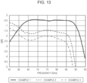
- FIG. 13 is a graph indicating pass characteristics of the waveguide converter 101 in the case of varying the distance H from the conversion portion S11 to the first surface 411.
- the graph includes a transverse axis indicating a frequency (GHz) of an input signal and an ordinate axis indicating a pass characteristic (dB).
- the graph indicating the pass characteristics also means that a signal has a smaller loss as the pass characteristic (dB) has a larger value (the same or a similar applies to FIG. 15 to be described later).
- the graph in FIG. 13 indicates the pass characteristics of the waveguide converter 101 with the distance H having the following three different values.
- the distance H is 0.35 mm (corresponding to 1/13.12 of the wavelength ⁇ at the frequency of 65 GHz or 1/9.85 of the wavelength ⁇ at the frequency of 87 GHz).
- the distance H is 1.154 mm (corresponding to 1/4 of the wavelength ⁇ at the frequency of 65 GHz).
- the distance H is 0.862 mm (corresponding to 1/4 of the wavelength ⁇ at the frequency of 87 GHz).
- the distance H from the conversion portion S11 to the first surface 411 is set to a value conventionally known as the distance with the short stub from the conversion portion S11 (1/4 of the wavelength ⁇ at the frequency of the signal transmitted through the signal conductor S1).
- FIG. 12 indicates the pass characteristics according to the respective examples, and includes a solid line indicating the pass characteristic according to example 1, a broken line indicating the pass characteristic according to example 2, and a dashed line indicating the pass characteristic according to example 3.
- example 1 achieves a better characteristic than examples 2 and 3 in the frequency band (65 GHz to 87 GHz) adopted by the waveguide 101.
- the first lid 4 may include a second surface 412 positioned to be overlapped with the second upper surface 2a, and a first recess 41 including a first opening 41O in the second surface 412.
- the first recess 41 includes the first surface 411.
- the first lid 4 including the first recess 41 allows accurate adjustment of a height of the back-short forming the short stub from the conversion portion S11 (the distance H from the conversion portion S11 to the first surface 411).
- the first opening 41O may be equal or less in area than the first region 1a1. In an embodiment, the first opening 41O may be equal or less in area than the first region 1a1 in a planar view, and the first opening 41O may be positioned inside the first region 1a1 in a planar view. Such a configuration as described above increases a bonded area between the first lid 4 and the first frame 3 to achieve improved bonding strength therebetween.
- the first lid 4 includes a portion that surrounds the first opening 41O and that may project in the x direction as illustrated in FIGs. 4 and 5 .
- Such a projecting portion is exemplarily indicated by Lx42. This configuration facilitates overlapping the first region 1a1 with the first opening 410 in a planar view.
- the first upper surface 1a may include the third region 1a3 connected to the second region 1a2 and positioned apart from the first region 1a1.
- the first frame 2 further includes a fifth end portion 25 and a sixth end portion 26 positioned to face each other and interpose the third region 1a3 in a planar view.
- the second region 1a2 is positioned between the first region 1a1 and the third region 1a3 in a planar view.
- the distance L12 in the y direction between the first end portion 21 and the second end portion 22 is equal to or less than a distance L56 in the y direction between the fifth end portion 25 and the sixth end portion 26.
- the first ground conductor G1 and the signal conductor S1 are connected to the electronic component 104 to be described later in the third region 1a3 by a connector such as a wire.
- the third region 1a3 is larger in the y direction than the second region 1a2 in a planar view so as to facilitate connecting the electronic component 104 to each of the first ground conductor G1 and the signal conductor S1 by the connector such as a wire.
- the line portion S12 may include a first portion S12a.
- the first portion S12a has a size Ls1 in the y direction corresponding to a maximum size in the y direction of the line portion S12. That is, the size Ls1 in the y direction of the first portion S12a is more than a size Ls4 in the y direction of the line portion S12 excluding the first portion S12a.
- Such a configuration as described above allows the line portion S12 to have more capacitance components and enables impedance adjustment. Accordingly, the signal conductor S1 is improved in radio-frequency characteristics, and the waveguide converter 101 is applicable to a wider frequency band.
- the line portion S12 can have more capacitance components also by decreasing a distance in the y direction between the line portion S12 and the first ground conductor G1 positioned to interpose the line portion S12. This configuration is thus effective in the same or a similar manner to the above case.
- the line portion S12 is positioned to extend to the third region 1a3 in a planar view.
- the first portion S12a is positioned from the second region 1a2 to the third region 1a3 in a planar view.
- the first portion S12a may be positioned only in the second region 1a2 or only in the third region 1a3.
- the line portion S12 may include a plurality of first portions S12a.
- the size Ls1 in the y direction of the first portion S12a is less than a size Ls11 in the y direction of the conversion portion S11, but can be changed in accordance with the frequency of the signal transmitted through the signal conductor S1. That is, the size Ls1 in the y direction of the first portion S12a may be more than or equal to the size Ls11 in the y direction of the conversion portion S11.
- FIG. 14 is a graph indicating reflection characteristics of the waveguide converter 101 in cases where the line portion S12 includes and does not include the first portion S12a.
- the line portion S12 includes the first portion S12a in example 1 whereas the line portion S12 does not include the first portion S12a in example 4.
- FIG. 14 indicates the reflection characteristics according to the respective examples, and includes a solid line indicating the reflection characteristic according to example 1, and a broken line indicating the reflection characteristic according to example 4.
- example 1 achieves a wider frequency band with the reflection characteristic of -15 dB or less.
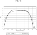
- FIG. 15 is a graph indicating pass characteristics of the waveguide converter 101 in the cases where the line portion S12 includes and does not include the first portion S12a.
- the line portion S12 includes the first portion S12a in example 1 whereas the line portion S12 does not include the first portion S12a in example 4.
- FIG. 15 indicates the pass characteristics according to the respective examples, and includes a solid line indicating the pass characteristic according to example 1, and a broken line indicating the pass characteristic according to example 4.
- example 1 achieves a wider frequency band with the pass characteristic of -0.6 dB or more.
- a distance Ls13 in the x direction from the conversion portion S11 to the first portion S12a in a planar view may be equal to or more than 5/8 and equal to or less than 7/8 of the wavelength ⁇ of the signal transmitted through the signal conductor S1.
- an inductive component is increased when the distance in the x direction from the conversion portion S11 is around 3/4 of the wavelength ⁇ of the transmitted signal.
- the signal conductor S1 can thus be improved in radio-frequency characteristics.
- the distance Ls13 can be set from a center point in the x direction and the y direction of the conversion portion S11 to a center point in the x direction and the y direction of the first portion S12a.
- FIG. 16 is a graph indicating reflection characteristics of the waveguide converter 101 in a case of varying the distance Ls13 in the x direction from the line portion S12 to the first portion S12a.
- the distance Ls13 according to example 1 is around 3/4 of the wavelength ⁇ of the signal transmitted through the signal conductor S1
- the distance Ls13 according to example 5 is around 1/2 of the wavelength ⁇ of the signal
- the distance Ls13 according to example 6 is around 7/8 of the wavelength ⁇ of the signal.
- FIG. 16 indicates the reflection characteristics according to the respective examples, and includes a solid line indicating the reflection characteristic according to example 1, a broken line indicating the reflection characteristic according to example 5, and a dashed line indicating the reflection characteristic according to example 6.
- example 1 achieves a better characteristic than examples 5 and 6.
- the distance Ls13 in the x direction from the conversion portion S11 to the first portion S12a in a planar view may be equal to or more than 1/8 and equal to or less than 3/8 of the wavelength ⁇ of the signal transmitted through the signal conductor S1.
- the inductive component is increased when the distance in the x direction from the conversion portion S11 is around 1/4 of the wavelength ⁇ of the transmitted signal.
- the signal conductor S1 can thus be improved in radio-frequency characteristics.
- the second surface 412 of the first lid 4 may include a first side 412a positioned to be overlapped with the second region 1a2 in a planar view.
- at least part of the first portion S12a of the line portion S12 is positioned to be overlapped with the first side 412a in a planar view.
- the first side 412a constitutes part of an outer circumference of the second surface 412.
- the conversion portion S11 may include a second portion S11b connected to the line portion S12.
- the line portion S12 may further include a third portion S12b connected to the second portion S11b.
- the size Ls11 in the y direction of the conversion portion S11 is larger than a size Ls3 in the y direction of the third portion S12b.
- the second portion S11b has a size Ls2 in the y direction gradually decreased outward in the x direction (a negative direction along an x axis in an embodiment).
- Such a configuration as described above is less likely to cause a rapid impedance variation from the conversion portion S11 to the line portion S12 to moderate mode conversions at the signal conductor S1 and the waveguide 107. This is less likely to cause a rapid deterioration in reflection characteristics due to positional displacement or the like in a case where the waveguide 107 is positioned under the conversion portion S11.
- the waveguide converter 101 may be exemplarily manufactured with use of a 3D printer.
- the first substrate 1 and the first frame 2 are not necessarily made of a same material as in the following manufacturing method.
- FIG. 11 is an exploded perspective view of the waveguide conversion device 10 including the electronic component mounting package 100 including the waveguide converter 101 according to an embodiment of the present disclosure.
- the electronic component mounting package 100 includes a second substrate 102, the waveguide converter 101, and a third frame 103.
- the second substrate 102 includes a third upper surface 102a, a third lower surface 102b opposite to the third upper surface 102a, and a through-hole 102H.
- the second substrate 102 exemplarily has a quadrilateral shape in a planar view having 10 mm ⁇ 10 mm to 100 mm ⁇ 100 mm in size and 0.5 mm to 20 mm in thickness.
- the second substrate 102 is made of a material, examples of which include metallic materials such as copper, iron, tungsten, molybdenum, nickel, and cobalt, and an alloy containing some of these metallic materials.
- the second substrate 102 may be constituted by a single metal plate or a stacked body including a plurality of stacked metal plates.
- the second substrate 102 may be provided on its surface with a plated layer of nickel, gold, or the like in accordance with an electroplating method or an electroless plating method for suppression of oxidation corrosion.
- the second substrate 102 may alternatively be made of an insulating material, examples of which include a ceramic material such as an aluminum oxide sintered body, a mullite sintered body, a silicon carbide sintered body, an aluminum nitride sintered body, a silicon nitride sintered body, or a glass ceramic.
- the through-hole 102H penetrates from the third upper surface 102a to the third lower surface 102b.
- the waveguide converter 101 is positioned on the third upper surface 102a to be overlapped with the through-hole 102H in a planar view.
- the through-hole 102H is positioned to be overlapped with the first region 1a1 and the conversion portion S11 in a planar view.
- the through-hole 102H is positioned to be overlapped with the waveguide 107 to be described later in a planar view.
- the third frame 103 is bonded to the third upper surface 102a and is positioned to surround the waveguide converter 101.
- the third frame 103 exemplarily has a quadrilateral shape in a planar view having 10 mm ⁇ 10 mm to 100 mm ⁇ 100 mm in size and 0.5 mm to 20 mm in thickness.
- the third frame 103 is made of a material that may be the same as or different from the material for the second substrate 102, and examples of the material for the third frame 103 include materials the same as or similar to the examples of the material for the first frame 2.
- the third frame 103 may include a wiring portion configured to be electrically connected to the electronic component 104 to be described later.
- the wiring portion may be formed on a green sheet forming an outer shape of the third frame 103 with use of a metallic material such as gold, silver, copper, nickel, tungsten, molybdenum, or manganese.
- the wiring portion may be formed by sintering a metal paste or may be formed by applying a thin film forming technique such as an evaporation method or a sputtering method.
- Part of the wiring portion may be provided thereon with an insulating film made of a ceramic (e.g., alumina coating), a resin, or the like.
- the third frame 103 can be bonded to the second substrate 102 via a bonding material such as a brazing filler material.
- the brazing filler material is made of a material, examples of which include silver, copper, gold, aluminum, and magnesium, and may contain an additive such as nickel, cadmium, or phosphorus.
- the second substrate 102 may further include a second recess 102K including a second opening 102O provided in the third upper surface 102a.
- the second recess 102K includes the through-hole 102H described above.
- the waveguide converter 10 is positioned in the second recess 102K.
- the first substrate 1 includes a second side 12 and a third side 13 connected to the second side 12 via a first corner portion 1K in a planar view.
- the second opening 102O includes a fourth side 1024 and a fifth side 1025 connected to the fourth side 1024 via a second corner portion 1026 in a planar view.
- the second side 12 is in contact with at least part of the fourth side 1024.
- the third side 13 is in contact with at least part of the fifth side 1025.
- Such a configuration allows the waveguide converter 101 to be mounted onto the second substrate 102 while the first substrate 1 of the waveguide converter 101 is in contact with the fourth side 1024 and the fifth side 1025.
- the waveguide converter 101 can thus be mounted onto the second substrate 102 with high positional accuracy.
- the signal conductor S1 is positioned on the second side 12. In the case where the electronic component 104 and the signal conductor S1 are electrically connected to each other via a connector such as a wire, this configuration is less likely to cause positional displacement in a direction (the x direction) in which the wire is connected and can reduce an impedance variation.
- any corner portion may correspond to the first corner portion 1K. Determination of the first corner portion 1K allows the second side 12 and the third side 13 to be determined uniquely. Furthermore, determination of the second side 12 and the third side 13 allows the fourth side 1024 and the fifth side 1025 to be determined uniquely.
- the corner portions (including the first corner portion 1K) of the first substrate 1 may each have a rectangular shape with a corner cut off into an arc shape. Such a configuration is less likely to cause damage to the first substrate 1 upon manufacture of the waveguide converter 101 and upon mounting the waveguide converter 101 onto the second substrate 102.
- the first frame 2 and the second frame 3 may each have a rectangular shape in a planar view with each corner cut off into an arc shape. Such a configuration can achieve the above effect in the same or a similar manner.
- the corner portions (including the first corner portion 1K) of the first substrate 1 are not limited to the above embodiment and may each have a rectangular shape with a round corner or the like.
- the waveguide conversion device 10 includes at least the electronic component mounting package 100, the electronic component 104, a second lid 106, and the waveguide 107.
- the electronic component 104 is positioned on the third upper surface 102a of the second substrate 102, and is electrically connected to the waveguide converter 101 in the electronic component mounting package 100.
- the electronic component 104 may be configured to process a signal, e.g., convert an optical signal to an electrical signal or convert an electrical signal to an optical signal.
- the electronic component 104 and the waveguide converter 101 are electrically connected to each other by a connector such as a wire made of a conductive metallic material.
- the electronic component 104 and the third frame 103 may be electrically connected to each other by a connector such as a wire.
- the electronic component 104 may be mounted directly on a second base 102, or may be mounted via a seat component such as a submount.
- the second lid 106 is positioned on the third frame 103 to cover the interior of the electronic component mounting package 100.
- the second lid 106 and the second frame 103 protect the electronic component 104.
- the second lid 106 exemplarily has a quadrilateral shape in a planar view having 10 mm ⁇ 10 mm to 50 mm ⁇ 50 mm in size and 0.5 mm to 2 mm in thickness.
- the second lid 106 is made of a material, examples of which include metallic materials such as iron, copper, nickel, chrome, cobalt, molybdenum, and tungsten, and an alloy obtained by combining some of these metallic materials.
- a metal member constituting the second lid 106 can be manufactured by applying a metalworking method such as a metal rolling method or a punching method to an ingot made of such a metallic material.
- the second lid 106 may be bonded to the third frame 103 via a seal ring or the like, or may be bonded via a bonding material such as solder, a brazing filler material, glass, or a resin adhesive.
- the waveguide 107 is positioned adjacent to the third lower surface 102b of the second substrate 102.
- the waveguide 107 is made of a material, examples of which include a conductor such as a metal.
- the second substrate 102 and the waveguide 107 may interpose a printed circuit board (PCB) or the like, and the second substrate 102 (the electronic component mounting package 100) may be bonded to the waveguide 107 via the printed circuit board or the like.
- PCB printed circuit board
- the waveguide converter configured as described above can enhance strength of the waveguide converter and is less likely to cause damage to the first substrate.
- characterized portions may be combined variously without being limited to exemplifications according to the above embodiment. Furthermore, combination is applicable among embodiments.
- the present disclosure is applicable to a waveguide converter, an electronic component mounting package, and a waveguide conversion device.
Landscapes
- Waveguides (AREA)
Abstract
Description
- The present disclosure relates to a waveguide converter, an electronic component mounting package, and a waveguide conversion device.
- Wireless communication has been adopting a higher frequency band along with requests for increases in speed and volume of the wireless communication. Accordingly, signals to be processed by wireless devices have also been adopting higher frequencies.
- Examples of a transmission medium configured to efficiently transmit such a radio-frequency signal include a waveguide. However, a waveguide cannot be connected directly to an integrated circuit mounted on a circuit board. Therefore widely adopted is a configuration in which the integrated circuit and the waveguide interpose a microstrip line. Adopting such a configuration needs a converter configured to mutually convert a signal between the waveguide and the microstrip line.
-
Patent Literature 1 describes a known invention relating to such a converter. According to the invention described inPatent Literature 1, a converter includes a waveguide-planar line conversion substrate including a dielectric substrate provided with a ground layer and a signal line configured to propagate a radio-frequency signal, and a housing including a waveguide. The waveguide-planar line conversion substrate includes an upper surface provided with a short lid (seeFIG. 1 and the like of Patent Literature 1). - Patent Literature 1:
Japanese Unexamined Patent Application Publication No. 2004-96206 - In an embodiment of the present disclosure, a waveguide converter (1) includes a first substrate, a signal conductor, a first ground conductor, a first frame, a second ground conductor, and a first lid. The first substrate includes a first upper surface including a first region and a second region extending from the first region. The signal conductor includes a conversion portion positioned in the first region, and a line portion connected to the conversion portion and positioned to extend at least from the first region to the second region. The first ground conductor is positioned to interpose the line portion at least in the second region on the first upper surface in a plannar view. The first frame includes a second upper surface and an inner surface connected to the second upper surface. The first frame is positioned on the first upper surface to surround at least part of the first region and the second region in a planar view. The first frame is made of a nonmetallic material. The second ground conductor is positioned on the second upper surface. The first lid is positioned on the second upper surface to cover the first region in a planar view. The first lid is made of a metallic material. The first frame further includes a first end portion and a second end portion positioned to face each other and interpose the second region in a planar view. The first ground conductor, the second ground conductor, and the first lid are electrically connected to one another.
- (2) The waveguide converter according to (1) described above further includes a second frame made of a nonmetallic material. The second frame is positioned on the second upper surface to surround at least part of the first region outside the inner surface in a planar view. Assuming that the line portion extends in a first direction and a second direction crosses the first direction in a planar view, the second frame includes a third end portion and a fourth end portion positioned to face each other in the second direction in a planar view.
- (3) In the waveguide converter according to (2) described above, a distance in the second direction between the first end portion and the second end portion is equal to or less than a distance in the second direction between the third end portion and the fourth end portion.
- (4) In the waveguide converter according to (1) to (3) described above, the first lid includes a first surface positioned to face the first region. In a sectional view crossing the first upper surface, a distance from the conversion portion to the first surface is equal to or more than 1/13.12 and equal to or less than 1/9.85 of a wavelength λ of a signal transmitted through the signal conductor.
- (5) In the waveguide converter according to (1) to (4) described above, the first lid includes a second surface positioned to be overlapped with the second upper surface, and a first recess including a first opening in the second surface. The first opening is equal or less in area than the first region in a planar view.
- (6) In the waveguide converter according to (1) to (4) described above, the first lid includes a second surface positioned to be overlapped with the second upper surface, and a first recess including a first opening in the second surface. The first recess includes the first surface.
- (7) In the waveguide converter according to (1) to (6) described above, the first upper surface includes a third region connected to the second region and positioned apart from the first region. The first frame further includes a fifth end portion and a sixth end portion positioned to face each other and interpose the third region in a planar view. The second region is positioned between the first region and the third region in a planar view. Assuming that the line portion extends in a first direction and a second direction crosses the first direction in a planar view, a distance in the second direction between the first end portion and the second end portion is equal to or less than a distance in the second direction between the fifth end portion and the sixth end portion.
- (8) In the waveguide converter according to (2) to (7) described above, the line portion includes a first portion. The first portion is positioned apart from the conversion portion in a planar view. A size in the second direction of the first portion is a maximum size in the second direction of the line portion.
- (9) In the waveguide converter according to (8) described above, a distance in the first direction from the conversion portion to the first portion in a planar view is equal to or more than 5/8 and equal to or less than 7/8 of a wavelength λ of a signal transmitted through the signal conductor.
- (10) In the waveguide converter according to (8) described above, a distance in the first direction from the conversion portion to the first portion in a planar view is equal to or more than 1/8 and equal to or less than 3/8 of a wavelength λ of a signal transmitted through the signal conductor.
- (11) In the waveguide converter according to (8) to (10) described above, the second surface includes a first side positioned to be overlapped with the second region in a planar view. At least part of the first portion is positioned to be overlapped with the first side in a planar view.
- (12) In the waveguide converter according to (1) to (11) described above, assuming that the line portion extends in a first direction and a second direction crosses the first direction in a planar view, the conversion portion includes a second portion connected to the line portion. The line portion includes a third portion connected to the second portion. A size in the second direction of the conversion portion is more than a size in the second direction of the third portion. A size in the second direction of the second portion gradually decreases outward in the first direction.
- (13) In an embodiment of the present disclosure, an electronic component mounting package includes a second substrate, the waveguide converter according to (1) to (12) described above, and a third frame. The second substrate includes a third upper surface, a third lower surface opposite to the third upper surface, and a through-hole. The through-hole penetrates from the third upper surface to the third lower surface. The waveguide converter according to (1) to (12) described above is positioned on the third upper surface to be overlapped with the through-hole in a planar view. The third frame is bonded to the third upper surface and is positioned to surround the waveguide converter.
- (14) In the electronic component mounting package according to (13) described above, the second substrate further includes a second recess including a second opening in the third upper surface. The second recess includes the through-hole. The waveguide converter according to (1) to (12) described above is positioned in the second recess. The first substrate includes a second side and a third side connected to the second side via a first corner portion in a planar view. The second opening includes a fourth side and a fifth side connected to the fourth side via a second corner portion in a planar view. The second side is in contact with at least part of the fourth side. The third side is in contact with at least part of the fifth side.
- (15) In an embodiment of the present disclosure, a waveguide conversion device includes the electronic component mounting package according to (13) or (14) described above, an electronic component, a second lid, and a waveguide. The electronic component is positioned on the third upper surface of the second substrate, and is electrically connected to a waveguide converter of the electronic component mounting package. The second lid is positioned on the third frame to cover an interior of the electronic component mounting package. The waveguide is positioned adjacent to the third lower surface of the second substrate.
-
-
FIG. 1 is an exploded perspective view of a waveguide converter according to an embodiment of the present disclosure. -
FIG. 2 is a perspective view of a waveguide converter according to an embodiment of the present disclosure. -
FIG. 3 is a perspective view from a different angle of a waveguide converter according to an embodiment of the present disclosure. -
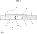
FIG. 4 is a sectional view taken along line Z1-Z1 of the waveguide converter illustrated inFIG. 2 . -
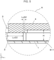
FIG. 5 is an enlarged view of a principal part A indicated inFIG. 4 . -
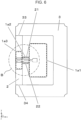
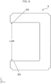
FIG. 6 is a plan view of a waveguide converter excluding a first lid according to an embodiment of the present disclosure. -
FIG. 7 is an enlarged view of a principal part B indicated inFIG. 6 . -
FIG. 8 is a plan view of a first frame according to an embodiment of the present disclosure. -
FIG. 9 is a plan view of a second frame according to an embodiment of the present disclosure. -
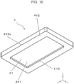
FIG. 10 is a perspective view of a first lid according to an embodiment of the present disclosure. -
FIG. 11 is an exploded perspective view of a waveguide conversion device according to an embodiment of the present disclosure. -
FIG. 12 is a graph indicating reflection characteristics of waveguide converters according to examples 1, 2, and 3. -
FIG. 13 is a graph indicating pass characteristics of the waveguide converters according to examples 1, 2, and 3. -
FIG. 14 is a graph indicating reflection characteristics of waveguide converters according to examples 1 and 4. -
FIG. 15 is a graph indicating pass characteristics of the waveguide converters according to examples 1 and 4. -
FIG. 16 is a graph indicating reflection characteristics of waveguide converters according to examples 1, 5, and 6. - An exemplary embodiment of the present disclosure will be described hereinafter with reference to the drawings. A waveguide converter may be disposed to include a top or a bottom in any direction. For convenience, the waveguide converter is defined to have an orthogonal coordinate system xyz, and a positive side in a z direction is assumed to indicate an upper side. The present disclosure refers to a first direction exemplarily indicating an x direction in the drawings. A second direction crossing the first direction exemplarily indicates a y direction in the drawings. The present disclosure refers to an outward direction exemplarily indicating a direction away from a first region 1a1 to be described later in the x direction or the y direction. The present disclosure refers to a planar view as a concept inclusive of a plan perspective view.
- Description is made to a
waveguide converter 101 according to the embodiment of the present disclosure with reference toFIGs. 1 to 10 . Thewaveguide converter 101 includes afirst substrate 1, a signal conductor S1, a first ground conductor G1, afirst frame 2, a second ground conductor G2, and afirst lid 4. - As illustrated in
FIGs. 1 and6 , thefirst substrate 1 includes a first upper surface 1a including the first region 1a1 and a second region 1a2 extending from the first region 1a1. Thefirst substrate 1 is made of a nonmetallic material or the like. Examples of the material for thefirst substrate 1 can include nonmetallic materials including a ceramic material such as an aluminum oxide sintered body, a mullite sintered body, a silicon carbide sintered body, an aluminum nitride sintered body, or a silicon nitride sintered body, and a glass ceramic material. Thefirst substrate 1 may alternatively be constituted by a printed circuit board such as a copper-clad laminate. - The
first substrate 1 may be constituted by a single layer made of a nonmetallic material or a multilayered product made of a nonmetallic material. Thefirst substrate 1 exemplarily has a rectangular shape in a planar view having 4 mm × 4 mm to 50 mm × 50 mm in size and 0.05 mm to 1 mm in thickness. - Though not illustrated, the
first substrate 1 may include a single or a plurality of via holes. The via hole can be formed by providing thefirst substrate 1 with a bore having an outer shape of the via hole and filling the bore with a conductive paste containing refractory metal powder of tungsten, molybdenum, or the like. - As illustrated in
FIG. 3 , thefirst substrate 1 further includes a firstlower surface 1b. The firstlower surface 1b may be provided with a third ground conductor G3. The third ground conductor G3 may be an annular metal layer positioned to surround the first region 1a1 in a planar view. The third ground conductor G3 may be electrically connected to the first ground conductor G1 to be described later by mean of the via hole or the like. The third ground conductor G3 positioned on the firstlower surface 1b can enhance ground potential of the signal conductor S1, as well as can serve as a conductive wall electromagnetically connected to awaveguide 107 to be described later. - The
first frame 2 includes a secondupper surface 2a and aninner surface 2c connected to the secondupper surface 2a. Thefirst frame 2 is positioned on the first upper surface 1a to surround at least part of the first region 1a1 and the second region 1a2 in a planar view. Thefirst frame 2 further includes afirst end portion 21 and asecond end portion 22 positioned to face each other and interpose the second region 1a2 in a planar view. Thefirst frame 2 is made of a nonmetallic material. The material for thefirst frame 2 may be the same as or different from the material for thefirst substrate 1, and examples of the material for thefirst frame 2 include materials the same as or similar to the examples of the material for thefirst substrate 1. In a case where thefirst substrate 1 and thefirst frame 2 are each made of a ceramic material or a glass ceramic material, thefirst substrate 1 and thefirst frame 2 can be manufactured by stacking green sheets formed into outer shapes of thefirst substrate 1 and thefirst frame 2. This can facilitate manufacture of thewaveguide converter 101. Thefirst frame 2 exemplarily has a U shape in a planar view having 4 mm × 4 mm to 50 mm × 50 mm in size and 0.1 mm to 5 mm in thickness. - The
first frame 2 is positioned on the first upper surface 1a of thefirst substrate 1 to achieve a reduction in a possibility of damage to thefirst substrate 1 as well as a reduction in the thickness of thefirst substrate 1 for excellent radio-frequency characteristics. - The
first frame 2 may alternatively be provided with a via hole in the same or a similar manner to thefirst substrate 1. Provision of the via hole can facilitate electrical connection of the first ground conductor G1 to be described later, the second ground conductor G2, and thefirst lid 4. The via hole can be formed in the same or a similar manner to the via hole provided in thefirst substrate 1. - The signal conductor S1 includes a conversion portion S11 positioned in the first region 1a1, and a line portion S12 connected to the conversion portion S11 and positioned to extend at least from the first region 1a1 to the second region 1a2. The signal conductor S1 is made of a material, examples of which include metallic materials such as gold, silver, copper, nickel, tungsten, molybdenum, and manganese. The signal conductor S1 may be formed by sintering a metal paste on the first upper surface 1a of the
first substrate 1, or may be formed by applying a thin film forming technique such as an evaporation method or a sputtering method. Part of the signal conductor S1 may be provided thereon with an insulating film made of a ceramic (e.g., alumina coating), a resin, or the like. The insulating film can be formed on the signal conductor S1 by screen printing. The insulating film may alternatively be positioned only on part of the conversion portion S11 or the line portion S12. Such a configuration is less likely to cause a short circuit between the signal conductor S1 and the first ground conductor G1 to be described later. - Though not illustrated, the signal conductor S1 may be electrically connected to an
electronic component 104 to be described later via a connector such as a wire principally made of a conductive metallic material such as platinum. Examples of the signal conductor S1 include a transmission line configured suitably for transmission of a radio-frequency signal such as a millimeter wave. A signal transmitted through the line portion S12 is electromagnetically coupled to thewaveguide 107 to be described later in the conversion portion S11. - The first ground conductor G1 is positioned to interpose the line portion S12 at least in the second region 1a2 on the first upper surface 1a in a planar view. The first ground conductor G1 is made of a material that may be the same as or different from the material for the signal conductor S1, and examples of the material for the first ground conductor G1 include materials the same as or similar to the examples of the material for the signal conductor S1. The first ground conductor G1 may be formed in the same or a similar manner to the signal conductor S1. In an embodiment, the signal conductor S1 and the first ground conductor G1 are positioned also in a third region 1a3 to be described later, and the first ground conductor G1 is positioned to interpose the line portion S12 in a planar view also in the third region 1a3. The signal conductor S1 is positioned to be interposed by the first ground conductor G1 to enhance ground potential and strengthen electric field coupling. This is less likely to cause a resonance generated by an electric field distribution expanding beyond a desired range when a radio-frequency signal is transmitted through the signal conductor S1.
- The first ground conductor G1 is not necessarily positioned to interpose the line portion S12 in a planar view in the third region 1a3. The first ground conductor G1 may include a pair of metal films separately provided on the first upper surface 1a so as to be positioned to interpose the signal conductor S1.
- In the same or a similar manner to the signal conductor S1, the first ground conductor G1 may be electrically connected to the
electronic component 104 to be described later via a connector such as a wire. - The second ground conductor G2 is positioned on the second
upper surface 2a. The second ground conductor G2 is made of a material that may be the same as or different from the material for the signal conductor S1, and examples of the material for the second ground conductor G2 include materials the same as or similar to the examples of the material for the signal conductor S1. The second ground conductor G2 may be formed in the same or a similar manner to the signal conductor S1. Provision of the second ground conductor G2 facilitates bonding thefirst lid 4 to be described later to thefirst frame 2. - In an embodiment, the second ground conductor G2 is positioned continuously from the second
upper surface 2a to theinner surface 2c of thefirst frame 2 as illustrated inFIG. 1 . Though not illustrated, the second ground conductor G2 may be positioned continuously to a surface opposite to the secondupper surface 2a of the first frame 2 (a surface facing the first upper surface 1a). This facilitates electrical connection of the first ground conductor G1, the second ground conductor G2, and thefirst lid 4. Furthermore, ground potential can be enhanced to reduce a signal loss generated when a radio-frequency signal is transmitted through the signal conductor S1. In the case where the second ground conductor G2 is positioned continuously from the secondupper surface 2a to theinner surface 2c, the second ground conductor G2 is electrically connected to thefirst lid 4 to be described later so as to be regarded as a so-called dummy back-short block (in other words, conductor block). In still other words, thefirst frame 2 and thefirst lid 4 can be regarded as an integral lid. - As illustrated in
FIGs. 1 and2 , thefirst lid 4 is positioned on the secondupper surface 2a to cover the first region 1a1 in a planar view. Thefirst lid 4 is made of a metallic material. Thefirst lid 4 exemplarily has a quadrilateral shape in a planar view having 1 mm × 1 mm to 50 mm × 50 mm in size and 0.2 mm to 20 mm in thickness. Examples of the material for thefirst lid 4 include metallic materials such as iron, copper, nickel, chrome, cobalt, molybdenum, and tungsten, and an alloy obtained by combining some of these metallic materials. A metal member constituting thefirst lid 4 can be manufactured by applying a metalworking method such as a metal rolling method or a punching method to an ingot made of such a metallic material. Thefirst lid 4 allows a signal transmitted through the signal conductor S1 to efficiently enter thewaveguide 107. Thefirst lid 4 further allows a signal having propagated through thewaveguide 107 to efficiently enter the signal conductor S1. - The
first lid 4 can be bonded to thefirst frame 2 and the second ground conductor G2 by a bonding material. - The first ground conductor G1, the second ground conductor G2, and the
first lid 4 are electrically connected to one another. In an embodiment, the first ground conductor G1, the second ground conductor G2, and thefirst lid 4 are electrically connected by the first ground conductor G2 positioned to extend to the via hole and theinner surface 2c of thefirst frame 2. This can enhance ground potential. The present disclosure is not limited to the above embodiment as long as the first ground conductor G1, the second ground conductor G2, and thefirst lid 4 can be electrically connected to one another. - As illustrated in
FIGs. 1 to 3 and6 , thewaveguide converter 101 may further include asecond frame 3 made of a nonmetallic material. Thesecond frame 3 is positioned on the secondupper surface 2a to surround at least part of the first region 1a1 outside theinner surface 2c in a planar view. Thesecond frame 3 further includes athird end portion 33 and afourth end portion 34 positioned to face each other in the y direction in a planar view. Such a configuration as described above allows thefirst lid 4 being in contact with thesecond frame 3 to be bonded to thefirst frame 3 so as to accurately bond thefirst lid 4 to thefirst frame 3. That is, thesecond frame 3 serves as a positioning guide upon bonding thefirst lid 4. - The material for the
second frame 3 may be the same as or different from the material for thefirst frame 2, and examples of the material for thesecond frame 3 include materials the same as or similar to the examples of the material for thefirst frame 2. In a case where thefirst substrate 1, thefirst frame 2, and thesecond frame 3 are each made of a ceramic material or a glass ceramic material, thefirst substrate 1, thefirst frame 2, and thesecond frame 3 can be manufactured by stacking green sheets formed into outer shapes of thefirst substrate 1, thefirst frame 2, and thesecond frame 3. This can facilitate manufacture of thewaveguide converter 101. Thesecond frame 3 exemplarily has a U shape in a planar view having 4 mm × 4 mm to 50 mm × 50 mm in size and 0.1 mm to 5 mm in thickness. When thesecond frame 3 is principally made of a ceramic material or a glass ceramic material, thesecond frame 3 having the U shape is less likely to warp upon sintering. - As described above, the
second frame 3 is not limitedly to have the U shape as long as thesecond frame 3 can serve as the positioning guide upon bonding thefirst lid 4. Thesecond frame 3 may alternatively have an L shape, a shape obtained by halving and separating the U shape, or the like. - As described above, the
second frame 3 is positioned on the secondupper surface 2a to surround at least part of the first region 1a1 outside theinner surface 2c in a planar view. More specifically, thesecond frame 3 includes an inner edge positioned outside an inner edge of thefirst frame 2 in a planar view. In an embodiment, each of three sides of the inner edge of thesecond frame 3 and a corresponding one of three sides of the inner edge of thefirst frame 2 have a constant distance in a planar view. - In an embodiment, the
second frame 3 includes an outer edge matching outer edges of thefirst substrate 1 and thefirst frame 2 in a planar view. However, the outer edge of thesecond frame 3 does not necessarily match the outer edges of thefirst substrate 1 and thefirst frame 2. That is, the outer edge of thesecond frame 3 may be larger or smaller than the outer edges of thefirst substrate 1 and thefirst frame 2. - As illustrated in
FIG. 7 , further assuming that a distance in the x direction from the outer edge of thefirst frame 2 to both or one of thefirst end portion 21 and thesecond end portion 22 is Lx21 and that a size in the x direction of both or one of thefirst end portion 21 and thesecond end portion 22 is Lx22, Lx22 > Lx21 may be satisfied. This configuration can enlarge a region equipped with thelid 4. Thelid 4 can thus be positioned stably on thefirst frame 2. - As illustrated in
FIG. 8 , further assuming that a size in the x direction of a portion of the first frame opposite to a portion positioned to surround the second region 1a2 so as to interpose the first region 1a1 is Lx23, (Lx21 + Lx22) > Lx23 may be satisfied. Thesecond frame 3 can thus be positioned stably on thefirst frame 2 in this configuration. - As illustrated in
FIGs. 6 to 9 , a distance L12 (FIG. 8 ) in the y direction between thefirst end portion 21 and thesecond end portion 22 of thefirst frame 2 may be equal to or less than a distance L34 (FIG. 9 ) in the y direction between thethird end portion 33 and thefourth end portion 34 of thesecond frame 3. Such a configuration allows thefirst lid 4 to be fitted from an opened side (a portion interposed between thethird end portion 33 and the fourth end portion 34) of thesecond frame 3 upon bonding thefirst lid 4 to thefirst frame 2. This can facilitate manufacture of thewaveguide converter 101. - As illustrated in
FIG. 10 , thefirst lid 4 may include afirst surface 411 positioned to face the first region 1a1. In this case, as illustrated inFIGs. 4 and5 , in a sectional view crossing the first upper surface 1a (a sectional view taken along an xy plane inFIGs. 4 and5 ), a distance H from the conversion portion S11 to thefirst surface 411 is equal to or more than 1/13.12 and equal to or less than 1/9.85 of a wavelength λ of a signal transmitted through the signal conductor S1. In an embodiment, thewaveguide converter 101 is applied to awaveguide conversion device 10 configured to process signals having a frequency band from 65 GHz to 87 GHz. Thewaveguide converter 101 includes respective portions set such that thewaveguide converter 101 adopts the frequency band from 65 GHz to 87 GHz. The above configuration achieves reductions in an insertion loss and a return loss in the band from 65 GHz to 87 GHz. -
FIG. 12 is a graph indicating reflection characteristics of thewaveguide converter 101 in a case of varying the distance H from the conversion portion S11 to thefirst surface 411. The graph includes a transverse axis indicating a frequency (GHz) of an input signal and an ordinate axis indicating a reflection characteristic (dB). The graph indicating the reflection characteristics also means that a signal has less reflection as the reflection characteristic (dB) has a smaller value (the same or a similar applies toFIGs. 14 and16 to be described later). The graph inFIG. 12 indicates the reflection characteristics of thewaveguide converter 101 with the distance H having the following three different values. In example 1, the distance H is 0.35 mm (corresponding to 1/13.12 of the wavelength λ at the frequency of 65 GHz or 1/9.85 of the wavelength λ at the frequency of 87 GHz). In example 2, the distance H is 1.154 mm (corresponding to 1/4 of the wavelength λ at the frequency of 65 GHz). In example 3, the distance H is 0.862 mm (corresponding to 1/4 of the wavelength λ at the frequency of 87 GHz). In examples 2 and 3, the distance H from the conversion portion S11 to thefirst surface 411 is set to a value known as a distance with a short stub from the conversion portion S11 (1/4 of the wavelength λ at the frequency of the signal transmitted through the signal conductor S1).FIG. 12 indicates the reflection characteristics according to the respective examples, and includes a solid line indicating the reflection characteristic according to example 1, a broken line indicating the reflection characteristic according to example 2, and a dashed line indicating the reflection characteristic according to example 3. - According to
FIG. 12 , example 1 achieves a better characteristic than examples 2 and 3 in the frequency band (65 GHz to 87 GHz) adopted by thewaveguide 101. -
FIG. 13 is a graph indicating pass characteristics of thewaveguide converter 101 in the case of varying the distance H from the conversion portion S11 to thefirst surface 411. The graph includes a transverse axis indicating a frequency (GHz) of an input signal and an ordinate axis indicating a pass characteristic (dB). The graph indicating the pass characteristics also means that a signal has a smaller loss as the pass characteristic (dB) has a larger value (the same or a similar applies toFIG. 15 to be described later). The graph inFIG. 13 indicates the pass characteristics of thewaveguide converter 101 with the distance H having the following three different values. In example 1, the distance H is 0.35 mm (corresponding to 1/13.12 of the wavelength λ at the frequency of 65 GHz or 1/9.85 of the wavelength λ at the frequency of 87 GHz). In example 2, the distance H is 1.154 mm (corresponding to 1/4 of the wavelength λ at the frequency of 65 GHz). In example 3, the distance H is 0.862 mm (corresponding to 1/4 of the wavelength λ at the frequency of 87 GHz). In examples 2 and 3, the distance H from the conversion portion S11 to thefirst surface 411 is set to a value conventionally known as the distance with the short stub from the conversion portion S11 (1/4 of the wavelength λ at the frequency of the signal transmitted through the signal conductor S1).FIG. 12 indicates the pass characteristics according to the respective examples, and includes a solid line indicating the pass characteristic according to example 1, a broken line indicating the pass characteristic according to example 2, and a dashed line indicating the pass characteristic according to example 3. - According to
FIG. 13 , example 1 achieves a better characteristic than examples 2 and 3 in the frequency band (65 GHz to 87 GHz) adopted by thewaveguide 101. - As illustrated in
FIG. 10 , thefirst lid 4 may include asecond surface 412 positioned to be overlapped with the secondupper surface 2a, and afirst recess 41 including a first opening 41O in thesecond surface 412. Thefirst recess 41 includes thefirst surface 411. Thefirst lid 4 including thefirst recess 41 allows accurate adjustment of a height of the back-short forming the short stub from the conversion portion S11 (the distance H from the conversion portion S11 to the first surface 411). - The first opening 41O may be equal or less in area than the first region 1a1. In an embodiment, the first opening 41O may be equal or less in area than the first region 1a1 in a planar view, and the first opening 41O may be positioned inside the first region 1a1 in a planar view. Such a configuration as described above increases a bonded area between the
first lid 4 and thefirst frame 3 to achieve improved bonding strength therebetween. - In the case where the first opening 41O is less in area than the first region 1a1, the
first lid 4 includes a portion that surrounds the first opening 41O and that may project in the x direction as illustrated inFIGs. 4 and5 . Such a projecting portion is exemplarily indicated by Lx42. This configuration facilitates overlapping the first region 1a1 with thefirst opening 410 in a planar view. - As illustrated in
FIG. 6 , the first upper surface 1a may include the third region 1a3 connected to the second region 1a2 and positioned apart from the first region 1a1. As illustrated inFIG. 8 , thefirst frame 2 further includes afifth end portion 25 and asixth end portion 26 positioned to face each other and interpose the third region 1a3 in a planar view. The second region 1a2 is positioned between the first region 1a1 and the third region 1a3 in a planar view. The distance L12 in the y direction between thefirst end portion 21 and thesecond end portion 22 is equal to or less than a distance L56 in the y direction between thefifth end portion 25 and thesixth end portion 26. In this case, the first ground conductor G1 and the signal conductor S1 are connected to theelectronic component 104 to be described later in the third region 1a3 by a connector such as a wire. In such a configuration as described above, the third region 1a3 is larger in the y direction than the second region 1a2 in a planar view so as to facilitate connecting theelectronic component 104 to each of the first ground conductor G1 and the signal conductor S1 by the connector such as a wire. - As illustrated in
FIG. 7 , the line portion S12 may include a first portion S12a. The first portion S12a has a size Ls1 in the y direction corresponding to a maximum size in the y direction of the line portion S12. That is, the size Ls1 in the y direction of the first portion S12a is more than a size Ls4 in the y direction of the line portion S12 excluding the first portion S12a. Such a configuration as described above allows the line portion S12 to have more capacitance components and enables impedance adjustment. Accordingly, the signal conductor S1 is improved in radio-frequency characteristics, and thewaveguide converter 101 is applicable to a wider frequency band. - The line portion S12 can have more capacitance components also by decreasing a distance in the y direction between the line portion S12 and the first ground conductor G1 positioned to interpose the line portion S12. This configuration is thus effective in the same or a similar manner to the above case.
- In an embodiment, the line portion S12 is positioned to extend to the third region 1a3 in a planar view. The first portion S12a is positioned from the second region 1a2 to the third region 1a3 in a planar view. Alternatively, the first portion S12a may be positioned only in the second region 1a2 or only in the third region 1a3. Still alternatively, the line portion S12 may include a plurality of first portions S12a.
- In an embodiment, the size Ls1 in the y direction of the first portion S12a is less than a size Ls11 in the y direction of the conversion portion S11, but can be changed in accordance with the frequency of the signal transmitted through the signal conductor S1. That is, the size Ls1 in the y direction of the first portion S12a may be more than or equal to the size Ls11 in the y direction of the conversion portion S11.
-
FIG. 14 is a graph indicating reflection characteristics of thewaveguide converter 101 in cases where the line portion S12 includes and does not include the first portion S12a. The line portion S12 includes the first portion S12a in example 1 whereas the line portion S12 does not include the first portion S12a in example 4.FIG. 14 indicates the reflection characteristics according to the respective examples, and includes a solid line indicating the reflection characteristic according to example 1, and a broken line indicating the reflection characteristic according to example 4. - According to
FIG. 14 , in comparison to example 4, example 1 achieves a wider frequency band with the reflection characteristic of -15 dB or less. -
FIG. 15 is a graph indicating pass characteristics of thewaveguide converter 101 in the cases where the line portion S12 includes and does not include the first portion S12a. The line portion S12 includes the first portion S12a in example 1 whereas the line portion S12 does not include the first portion S12a in example 4.FIG. 15 indicates the pass characteristics according to the respective examples, and includes a solid line indicating the pass characteristic according to example 1, and a broken line indicating the pass characteristic according to example 4. - According to
FIG. 15 , in comparison to example 4, example 1 achieves a wider frequency band with the pass characteristic of -0.6 dB or more. - As illustrated in
FIG. 7 , a distance Ls13 in the x direction from the conversion portion S11 to the first portion S12a in a planar view may be equal to or more than 5/8 and equal to or less than 7/8 of the wavelength λ of the signal transmitted through the signal conductor S1. In the case where a radio-frequency signal is transmitted through the signal conductor S1, an inductive component is increased when the distance in the x direction from the conversion portion S11 is around 3/4 of the wavelength λ of the transmitted signal. Such a configuration as described above thus enables impedance adjustment. The signal conductor S1 can thus be improved in radio-frequency characteristics. The distance Ls13 can be set from a center point in the x direction and the y direction of the conversion portion S11 to a center point in the x direction and the y direction of the first portion S12a. -
FIG. 16 is a graph indicating reflection characteristics of thewaveguide converter 101 in a case of varying the distance Ls13 in the x direction from the line portion S12 to the first portion S12a. The distance Ls13 according to example 1 is around 3/4 of the wavelength λ of the signal transmitted through the signal conductor S1, the distance Ls13 according to example 5 is around 1/2 of the wavelength λ of the signal, and the distance Ls13 according to example 6 is around 7/8 of the wavelength λ of the signal.FIG. 16 indicates the reflection characteristics according to the respective examples, and includes a solid line indicating the reflection characteristic according to example 1, a broken line indicating the reflection characteristic according to example 5, and a dashed line indicating the reflection characteristic according to example 6. - According to
FIG. 16 , example 1 achieves a better characteristic than examples 5 and 6. - As illustrated in
FIG. 7 , the distance Ls13 in the x direction from the conversion portion S11 to the first portion S12a in a planar view may be equal to or more than 1/8 and equal to or less than 3/8 of the wavelength λ of the signal transmitted through the signal conductor S1. In the case where a radio-frequency signal is transmitted through the signal conductor S1, the inductive component is increased when the distance in the x direction from the conversion portion S11 is around 1/4 of the wavelength λ of the transmitted signal. Such a configuration as described above thus enables impedance adjustment. The signal conductor S1 can thus be improved in radio-frequency characteristics. - As illustrated in
FIG. 10 , thesecond surface 412 of thefirst lid 4 may include afirst side 412a positioned to be overlapped with the second region 1a2 in a planar view. In this case, at least part of the first portion S12a of the line portion S12 is positioned to be overlapped with thefirst side 412a in a planar view. Thefirst side 412a constitutes part of an outer circumference of thesecond surface 412. - As illustrated in
FIG. 7 , the conversion portion S11 may include a second portion S11b connected to the line portion S12. The line portion S12 may further include a third portion S12b connected to the second portion S11b. The size Ls11 in the y direction of the conversion portion S11 is larger than a size Ls3 in the y direction of the third portion S12b. The second portion S11b has a size Ls2 in the y direction gradually decreased outward in the x direction (a negative direction along an x axis in an embodiment). Such a configuration as described above is less likely to cause a rapid impedance variation from the conversion portion S11 to the line portion S12 to moderate mode conversions at the signal conductor S1 and thewaveguide 107. This is less likely to cause a rapid deterioration in reflection characteristics due to positional displacement or the like in a case where thewaveguide 107 is positioned under the conversion portion S11. - Description is made herein to a method of manufacturing the
waveguide converter 101 according to the embodiment of the present disclosure. The present disclosure is not limited to the following embodiment, and thewaveguide converter 101 may be exemplarily manufactured with use of a 3D printer. As described earlier, thefirst substrate 1 and thefirst frame 2 are not necessarily made of a same material as in the following manufacturing method. - (1) Initially formed is a plurality of green sheets. Specifically, an organic binder, a plasticizer, a solvent, or the like is added to be mixed with ceramic powder of boron nitride, aluminum nitride, silicon nitride, silicon carbide, beryllium oxide, or the like to obtain a mixture. The mixture thus obtained is layered to manufacture a plurality of green sheets. Subsequently, the plurality of green sheets is processed with use of dies or the like to prepare a plurality of green sheets formed into the outer shapes of the
first substrate 1 and thefirst frame 2 in a planar view. In a case where thefirst substrate 1 and thefirst frame 2 each include a via hole, a bore having an outer shape of the via hole is formed in each of thefirst substrate 1 and thefirst frame 2 by means of a die, laser cutting, or the like. In the case of forming thewaveguide converter 101 including thesecond frame 3, further prepared is a green sheet formed into the outer shape of thesecond frame 3. - (2) Refractory metal powder of tungsten, molybdenum, or the like is prepared, and an organic binder, a plasticizer, a solvent, or the like is added to be mixed with the powder to prepare a metal paste. Subsequently, the metal paste is printed to have a predetermined pattern on the plurality of green sheets formed into the outer shapes of the
first substrate 1 and thefirst frame 2 so as to form the signal conductor S1, the first ground conductor G1, and the second ground conductor G2. The metal paste may optionally contain glass or a ceramic in order to have higher bonding strength with thefirst substrate 1 and thefirst frame 2. The bores formed in thefirst substrate 1 and thefirst frame 2 in the step described above in (1) are filled with the metal paste to form via holes. - (3) The plurality of green sheets formed into the outer shapes of the
first substrate 1 and thefirst frame 2 is stacked to match outer edges to form a green sheet stacked body. Alternatively, the metal paste may be printed to have the predetermined pattern after the green sheet stacked body is formed, and the signal conductor S1, the first ground conductor G1, the second ground conductor G2, and other wiring (e.g., the third ground conductor G3) may then be formed. - (4) The green sheet stacked body is burned to sinter the plurality of green sheets so as to obtain a sintered body including the
first substrate 1 and thefirst frame 2 being stacked. - (5) A metalworking method such as a metal rolling method or a punching method is applied to an ingot made of a metallic material for the
first lid 4 to form thefirst lid 4. - (6) The
first lid 4 is bonded to the sintered body formed in the step described above in (4) with use of a bonding material to obtain thewaveguide converter 101. - With reference to
FIG. 11 , description is made next to an electroniccomponent mounting package 100 according to an embodiment of the present disclosure.FIG. 11 is an exploded perspective view of thewaveguide conversion device 10 including the electroniccomponent mounting package 100 including thewaveguide converter 101 according to an embodiment of the present disclosure. The electroniccomponent mounting package 100 includes asecond substrate 102, thewaveguide converter 101, and athird frame 103. - The
second substrate 102 includes a thirdupper surface 102a, a thirdlower surface 102b opposite to the thirdupper surface 102a, and a through-hole 102H. Thesecond substrate 102 exemplarily has a quadrilateral shape in a planar view having 10 mm × 10 mm to 100 mm × 100 mm in size and 0.5 mm to 20 mm in thickness. Thesecond substrate 102 is made of a material, examples of which include metallic materials such as copper, iron, tungsten, molybdenum, nickel, and cobalt, and an alloy containing some of these metallic materials. In this case, thesecond substrate 102 may be constituted by a single metal plate or a stacked body including a plurality of stacked metal plates. In the case where thesecond substrate 102 is made of any one of the above metallic materials, thesecond substrate 102 may be provided on its surface with a plated layer of nickel, gold, or the like in accordance with an electroplating method or an electroless plating method for suppression of oxidation corrosion. Thesecond substrate 102 may alternatively be made of an insulating material, examples of which include a ceramic material such as an aluminum oxide sintered body, a mullite sintered body, a silicon carbide sintered body, an aluminum nitride sintered body, a silicon nitride sintered body, or a glass ceramic. - The through-
hole 102H penetrates from the thirdupper surface 102a to the thirdlower surface 102b. Thewaveguide converter 101 is positioned on the thirdupper surface 102a to be overlapped with the through-hole 102H in a planar view. The through-hole 102H is positioned to be overlapped with the first region 1a1 and the conversion portion S11 in a planar view. The through-hole 102H is positioned to be overlapped with thewaveguide 107 to be described later in a planar view. - The
third frame 103 is bonded to the thirdupper surface 102a and is positioned to surround thewaveguide converter 101. Thethird frame 103 exemplarily has a quadrilateral shape in a planar view having 10 mm × 10 mm to 100 mm × 100 mm in size and 0.5 mm to 20 mm in thickness. Thethird frame 103 is made of a material that may be the same as or different from the material for thesecond substrate 102, and examples of the material for thethird frame 103 include materials the same as or similar to the examples of the material for thefirst frame 2. Thethird frame 103 may include a wiring portion configured to be electrically connected to theelectronic component 104 to be described later. The wiring portion may be formed on a green sheet forming an outer shape of thethird frame 103 with use of a metallic material such as gold, silver, copper, nickel, tungsten, molybdenum, or manganese. The wiring portion may be formed by sintering a metal paste or may be formed by applying a thin film forming technique such as an evaporation method or a sputtering method. Part of the wiring portion may be provided thereon with an insulating film made of a ceramic (e.g., alumina coating), a resin, or the like. - The
third frame 103 can be bonded to thesecond substrate 102 via a bonding material such as a brazing filler material. The brazing filler material is made of a material, examples of which include silver, copper, gold, aluminum, and magnesium, and may contain an additive such as nickel, cadmium, or phosphorus. - The
second substrate 102 may further include asecond recess 102K including a second opening 102O provided in the thirdupper surface 102a. Thesecond recess 102K includes the through-hole 102H described above. In this case, thewaveguide converter 10 is positioned in thesecond recess 102K. Thefirst substrate 1 includes asecond side 12 and athird side 13 connected to thesecond side 12 via afirst corner portion 1K in a planar view. The second opening 102O includes afourth side 1024 and afifth side 1025 connected to thefourth side 1024 via asecond corner portion 1026 in a planar view. Thesecond side 12 is in contact with at least part of thefourth side 1024. Thethird side 13 is in contact with at least part of thefifth side 1025. Such a configuration allows thewaveguide converter 101 to be mounted onto thesecond substrate 102 while thefirst substrate 1 of thewaveguide converter 101 is in contact with thefourth side 1024 and thefifth side 1025. Thewaveguide converter 101 can thus be mounted onto thesecond substrate 102 with high positional accuracy. In an embodiment, the signal conductor S1 is positioned on thesecond side 12. In the case where theelectronic component 104 and the signal conductor S1 are electrically connected to each other via a connector such as a wire, this configuration is less likely to cause positional displacement in a direction (the x direction) in which the wire is connected and can reduce an impedance variation. - In a case where the
first substrate 1 has a polygonal shape such as a rectangular shape, any corner portion may correspond to thefirst corner portion 1K. Determination of thefirst corner portion 1K allows thesecond side 12 and thethird side 13 to be determined uniquely. Furthermore, determination of thesecond side 12 and thethird side 13 allows thefourth side 1024 and thefifth side 1025 to be determined uniquely. - As in an embodiment, the corner portions (including the
first corner portion 1K) of thefirst substrate 1 may each have a rectangular shape with a corner cut off into an arc shape. Such a configuration is less likely to cause damage to thefirst substrate 1 upon manufacture of thewaveguide converter 101 and upon mounting thewaveguide converter 101 onto thesecond substrate 102. In the same or a similar manner, thefirst frame 2 and thesecond frame 3 may each have a rectangular shape in a planar view with each corner cut off into an arc shape. Such a configuration can achieve the above effect in the same or a similar manner. The corner portions (including thefirst corner portion 1K) of thefirst substrate 1 are not limited to the above embodiment and may each have a rectangular shape with a round corner or the like. - Description is made next to the
waveguide conversion device 10 according to an embodiment of the present disclosure. As illustrated inFIG. 11 , thewaveguide conversion device 10 includes at least the electroniccomponent mounting package 100, theelectronic component 104, asecond lid 106, and thewaveguide 107. - The
electronic component 104 is positioned on the thirdupper surface 102a of thesecond substrate 102, and is electrically connected to thewaveguide converter 101 in the electroniccomponent mounting package 100. Theelectronic component 104 may be configured to process a signal, e.g., convert an optical signal to an electrical signal or convert an electrical signal to an optical signal. Though not illustrated, theelectronic component 104 and thewaveguide converter 101 are electrically connected to each other by a connector such as a wire made of a conductive metallic material. Theelectronic component 104 and thethird frame 103 may be electrically connected to each other by a connector such as a wire. Theelectronic component 104 may be mounted directly on asecond base 102, or may be mounted via a seat component such as a submount. - The
second lid 106 is positioned on thethird frame 103 to cover the interior of the electroniccomponent mounting package 100. Thesecond lid 106 and thesecond frame 103 protect theelectronic component 104. Thesecond lid 106 exemplarily has a quadrilateral shape in a planar view having 10 mm × 10 mm to 50 mm × 50 mm in size and 0.5 mm to 2 mm in thickness. Thesecond lid 106 is made of a material, examples of which include metallic materials such as iron, copper, nickel, chrome, cobalt, molybdenum, and tungsten, and an alloy obtained by combining some of these metallic materials. A metal member constituting thesecond lid 106 can be manufactured by applying a metalworking method such as a metal rolling method or a punching method to an ingot made of such a metallic material. - The
second lid 106 may be bonded to thethird frame 103 via a seal ring or the like, or may be bonded via a bonding material such as solder, a brazing filler material, glass, or a resin adhesive. - The
waveguide 107 is positioned adjacent to the thirdlower surface 102b of thesecond substrate 102. Thewaveguide 107 is made of a material, examples of which include a conductor such as a metal. Thesecond substrate 102 and thewaveguide 107 may interpose a printed circuit board (PCB) or the like, and the second substrate 102 (the electronic component mounting package 100) may be bonded to thewaveguide 107 via the printed circuit board or the like. - In an embodiment, the waveguide converter configured as described above can enhance strength of the waveguide converter and is less likely to cause damage to the first substrate.
- This allows a reduction in the thickness of the first substrate to achieve excellent radio-frequency characteristics.
- In an embodiment, characterized portions may be combined variously without being limited to exemplifications according to the above embodiment. Furthermore, combination is applicable among embodiments.
- The present disclosure is applicable to a waveguide converter, an electronic component mounting package, and a waveguide conversion device.
-
- 1 first substrate
- 1a first upper surface
- 1a1 first region
- 1a2 second region
- 1a3 third region
- 1b first lower surface
- 12 second side
- 13 third side
- 1K first corner portion
- G1 first ground conductor
- G2 second ground conductor
- G3 third ground conductor
- S1 signal conductor
- S11 conversion portion
- S11b second portion
- S12 line portion
- S12a first portion
- S12b third portion
- 2 first frame
- 2a second upper surface
- 2c inner surface
- 21 first end portion
- 22 second end portion
- 25 fifth end portion
- 26 sixth end portion
- 3 second frame
- 33 third end portion
- 34 fourth end portion
- 4 first lid
- 41 first recess
- 41O first opening
- 411 first surface
- 412 second surface
- 412a first side
- L12 distance between first end portion and second end portion
- L34 distance between third end portion and fourth end portion
- L56 distance between fifth end portion and sixth end portion
- Ls1 size of first portion
- Ls2 size of second portion
- Ls3 size of third portion
- Ls4 size of line portion excluding first portion
- Ls11 size of conversion portion
- Ls13 distance from conversion portion to first portion
- H distance between conversion portion and first surface
- 10 waveguide conversion device
- 100 electronic component mounting package
- 101 waveguide converter
- 102 second substrate
- 102a third upper surface
- 102b third lower surface
- 1024 fourth side
- 1025 fifth side
- 1026 second corner portion
- 102K second recess
- 102O second opening
- 102H through-hole
- 103 third frame
- 104 electronic component
- 106 second lid
- 107 waveguide
Claims (15)
- A waveguide converter comprising:a first substrate including a first upper surface including a first region and a second region extending from the first region;a signal conductor including a conversion portion positioned in the first region and a line portion connected to the conversion portion and positioned to extend at least from the first region to the second region;a first ground conductor positioned to interpose the line portion at least in the second region on the first upper surface in a planar view;a first frame positioned on the first upper surface to surround at least part of the first region and the second region in a planar view, including a second upper surface and an inner surface connected to the second upper surface, and made of a nonmetallic material;a second ground conductor positioned on the second upper surface; anda first lid positioned on the second upper surface to cover the first region in a planar view, and made of a metallic material; whereinthe first frame further includes a first end portion and a second end portion positioned to face each other and interpose the second region in a planar view, andthe first ground conductor, the second ground conductor, and the first lid are electrically connected to one another.
- The waveguide converter according to claim 1,assuming that the line portion extends in a first direction and a second direction crosses the first direction in a planar view, the waveguide converter further comprisinga second frame positioned on the second upper surface to surround at least part of the first region outside the inner surface in a planar view and made of a nonmetallic material, whereinthe second frame includes a third end portion and a fourth end portion positioned to face each other in the second direction in a planar view.
- The waveguide converter according to claim 2, wherein a distance in the second direction between the first end portion and the second end portion is equal to or less than a distance in the second direction between the third end portion and the fourth end portion.
- The waveguide converter according to any one of claims 1 to 3, whereinthe first lid includes a first surface positioned to face the first region, andin a sectional view crossing the first upper surface, a distance from the conversion portion to the first surface is equal to or more than 1/13.12 and equal to or less than 1/9.85 of a wavelength λ of a signal transmitted through the signal conductor.
- The waveguide converter according to any one of claims 1 to 4, whereinthe first lid includes a second surface positioned to be overlapped with the second upper surface, and a first recess including a first opening in the second surface, andthe first opening is equal or less in area than the first region in a planar view.
- The waveguide converter according to any one of claims 1 to 4, whereinthe first lid includes a second surface positioned to be overlapped with the second upper surface, and a first recess including a first opening in the second surface, andthe first recess includes the first surface.
- The waveguide converter according to any one of claims 1 to 6, whereinthe first upper surface includes a third region connected to the second region and positioned apart from the first region,the first frame further includes a fifth end portion and a sixth end portion positioned to face each other and interpose the third region in a planar view,the second region is positioned between the first region and the third region in a planar view, andassuming that the line portion extends in a first direction and a second direction crosses the first direction in a planar view,a distance in the second direction between the first end portion and the second end portion is equal to or less than a distance in the second direction between the fifth end portion and the sixth end portion.
- The waveguide converter according to any one of claims 2, 3, and 7,
whereinthe line portion includes a first portion positioned apart from the conversion portion in a planar view, anda size in the second direction of the first portion is a maximum size in the second direction of the line portion. - The waveguide converter according to claim 8, wherein a distance in the first direction from the conversion portion to the first portion in a planar view is equal to or more than 5/8 and equal to or less than 7/8 of a wavelength λ of a signal transmitted through the signal conductor.
- The waveguide converter according to claim 8, wherein a distance in the first direction from the conversion portion to the first portion in a planar view is equal to or more than 1/8 and equal to or less than 3/8 of a wavelength λ of a signal transmitted through the signal conductor.
- The waveguide converter according to any one of claims 8 to 10, whereinthe second surface includes a first side positioned to be overlapped with the second region in a planar view, andat least part of the first portion is positioned to be overlapped with the first side in a planar view.
- The waveguide converter according to any one of claims 1 to 11, whereinassuming that the line portion extends in a first direction and a second direction crosses the first direction in a planar view,the conversion portion includes a second portion connected to the line portion,the line portion includes a third portion connected to the second portion,a size in the second direction of the conversion portion is more than a size in the second direction of the third portion, anda size in the second direction of the second portion gradually decreases outward in the first direction.
- An electronic component mounting package comprising:a second substrate including a third upper surface, a third lower surface opposite to the third upper surface, and a through-hole penetrating from the third upper surface to the third lower surface;the waveguide converter according to any one of claims 1 to 12, the waveguide converter positioned on the third upper surface to be overlapped with the through-hole in a planar view; anda third frame bonded to the third upper surface and positioned to surround the waveguide converter.
- The electronic component mounting package according to claim 13, whereinthe second substrate further includes a second recess including a second opening in the third upper surface,the second recess includes the through-hole,the waveguide converter is positioned in the second recess,the first substrate includes a second side and a third side connected to the second side via a first corner portion in a planar view,the second opening includes a fourth side and a fifth side connected to the fourth side via a second corner portion in a planar view,the second side is in contact with at least part of the fourth side, andthe third side is in contact with at least part of the fifth side.
- A waveguide conversion device comprising:the electronic component mounting package according to claim 13 or 14;an electronic component positioned on the third upper surface of the second substrate, and electrically connected to a waveguide converter in the electronic component mounting package;a second lid positioned on the third frame to cover an interior of the electronic component mounting package; anda waveguide positioned adjacent to the third lower surface of the second substrate.
Applications Claiming Priority (2)
| Application Number | Priority Date | Filing Date | Title |
|---|---|---|---|
| JP2022104801 | 2022-06-29 | ||
| PCT/JP2023/023926 WO2024005052A1 (en) | 2022-06-29 | 2023-06-28 | Waveguide converter, package for mounting electronic component, and waveguide conversion device |
Publications (1)
| Publication Number | Publication Date |
|---|---|
| EP4550567A1 true EP4550567A1 (en) | 2025-05-07 |
Family
ID=89382326
Family Applications (1)
| Application Number | Title | Priority Date | Filing Date |
|---|---|---|---|
| EP23831492.6A Withdrawn EP4550567A1 (en) | 2022-06-29 | 2023-06-28 | Waveguide converter, package for mounting electronic component, and waveguide conversion device |
Country Status (4)
| Country | Link |
|---|---|
| EP (1) | EP4550567A1 (en) |
| JP (1) | JP7716590B2 (en) |
| CN (1) | CN119422286A (en) |
| WO (1) | WO2024005052A1 (en) |
Family Cites Families (6)
| Publication number | Priority date | Publication date | Assignee | Title |
|---|---|---|---|---|
| JP2004096206A (en) | 2002-08-29 | 2004-03-25 | Fujitsu Ten Ltd | Waveguide / planar line converter, and high frequency circuit apparatus |
| FR2869725A1 (en) * | 2004-04-29 | 2005-11-04 | Thomson Licensing Sa | NON-CONTACT TRANSITION ELEMENT BETWEEN A WAVEGUIDE AND A MOCRORUBAN LINE |
| JP4568235B2 (en) * | 2006-02-08 | 2010-10-27 | 株式会社デンソー | Transmission line converter |
| JP2012178815A (en) * | 2011-01-31 | 2012-09-13 | Kyocera Corp | High-frequency module |
| JP2016072881A (en) * | 2014-09-30 | 2016-05-09 | 日本電産エレシス株式会社 | High frequency power conversion mechanism |
| JP6059746B2 (en) * | 2015-02-09 | 2017-01-11 | 株式会社フジクラ | converter |
-
2023
- 2023-06-28 WO PCT/JP2023/023926 patent/WO2024005052A1/en not_active Ceased
- 2023-06-28 EP EP23831492.6A patent/EP4550567A1/en not_active Withdrawn
- 2023-06-28 CN CN202380049111.9A patent/CN119422286A/en active Pending
- 2023-06-28 JP JP2024530909A patent/JP7716590B2/en active Active
Also Published As
| Publication number | Publication date |
|---|---|
| JP7716590B2 (en) | 2025-07-31 |
| JPWO2024005052A1 (en) | 2024-01-04 |
| WO2024005052A1 (en) | 2024-01-04 |
| CN119422286A (en) | 2025-02-11 |
Similar Documents
| Publication | Publication Date | Title |
|---|---|---|
| US20250056726A1 (en) | Wiring board, electronic component mounting package using wiring board, and electronic module | |
| US20250151200A1 (en) | Wiring board, electronic component mounting package using wiring board, and electronic module | |
| CN109863591B (en) | High-frequency substrate, high-frequency package and high-frequency module | |
| US20240405130A1 (en) | Wiring board, electronic component package, and electronic apparatus | |
| US6936921B2 (en) | High-frequency package | |
| WO2013099936A1 (en) | Input/output member, package for housing electronic component, and electronic apparatus | |
| JP2020005018A (en) | Differential transmission line, wiring board, and package for semiconductor | |
| US9805995B2 (en) | Element-accommodating package and mounting structure | |
| EP4550567A1 (en) | Waveguide converter, package for mounting electronic component, and waveguide conversion device | |
| US20250351264A1 (en) | Wiring board, electronic component mounting package using wiring board, and electronic module | |
| JP7432703B2 (en) | Wiring base and electronic equipment | |
| JP7027578B2 (en) | Wiring boards, electronic component storage packages and electronic devices | |
| EP4600998A1 (en) | Wiring board, electronic component mounting package using wiring board, and electronic module | |
| WO2022230848A1 (en) | Electronic component mounting package and electronic device | |
| US20260059654A1 (en) | Wiring board, electronic component mounting package including wiring board, and electronic module | |
| US11889618B2 (en) | Wiring board, electronic component package, and electronic apparatus | |
| JP4606351B2 (en) | High frequency line-waveguide converter | |
| JP4247999B2 (en) | High frequency line-waveguide converter | |
| JP2024048912A (en) | Wiring board, wiring structure using wiring board, package for mounting electronic components, and electronic module | |
| JP2021120985A (en) | Wiring base and electronic apparatus | |
| WO2024014433A1 (en) | Wiring structure and electronic module | |
| WO2021149491A1 (en) | Wiring substrate and electronic device | |
| JP2001189405A (en) | High frequency input / output terminals and high frequency semiconductor element storage package |
Legal Events
| Date | Code | Title | Description |
|---|---|---|---|
| STAA | Information on the status of an ep patent application or granted ep patent |
Free format text: STATUS: THE INTERNATIONAL PUBLICATION HAS BEEN MADE |
|
| PUAI | Public reference made under article 153(3) epc to a published international application that has entered the european phase |
Free format text: ORIGINAL CODE: 0009012 |
|
| STAA | Information on the status of an ep patent application or granted ep patent |
Free format text: STATUS: REQUEST FOR EXAMINATION WAS MADE |
|
| 17P | Request for examination filed |
Effective date: 20241223 |
|
| AK | Designated contracting states |
Kind code of ref document: A1 Designated state(s): AL AT BE BG CH CY CZ DE DK EE ES FI FR GB GR HR HU IE IS IT LI LT LU LV MC ME MK MT NL NO PL PT RO RS SE SI SK SM TR |
|
| STAA | Information on the status of an ep patent application or granted ep patent |
Free format text: STATUS: THE APPLICATION HAS BEEN WITHDRAWN |
|
| 18W | Application withdrawn |
Effective date: 20250804 |