EP4550429A1 - Light-emitting substrate and fabrication method therefor, and display apparatus - Google Patents
Light-emitting substrate and fabrication method therefor, and display apparatus Download PDFInfo
- Publication number
- EP4550429A1 EP4550429A1 EP22741416.6A EP22741416A EP4550429A1 EP 4550429 A1 EP4550429 A1 EP 4550429A1 EP 22741416 A EP22741416 A EP 22741416A EP 4550429 A1 EP4550429 A1 EP 4550429A1
- Authority
- EP
- European Patent Office
- Prior art keywords
- light
- substrate
- bonding pad
- emitting substrate
- emitting
- Prior art date
- Legal status (The legal status is an assumption and is not a legal conclusion. Google has not performed a legal analysis and makes no representation as to the accuracy of the status listed.)
- Pending
Links
Images




Classifications
-
- H—ELECTRICITY
- H10—SEMICONDUCTOR DEVICES; ELECTRIC SOLID-STATE DEVICES NOT OTHERWISE PROVIDED FOR
- H10H—INORGANIC LIGHT-EMITTING SEMICONDUCTOR DEVICES HAVING POTENTIAL BARRIERS
- H10H20/00—Individual inorganic light-emitting semiconductor devices having potential barriers, e.g. light-emitting diodes [LED]
- H10H20/80—Constructional details
- H10H20/85—Packages
- H10H20/852—Encapsulations
-
- H—ELECTRICITY
- H10—SEMICONDUCTOR DEVICES; ELECTRIC SOLID-STATE DEVICES NOT OTHERWISE PROVIDED FOR
- H10H—INORGANIC LIGHT-EMITTING SEMICONDUCTOR DEVICES HAVING POTENTIAL BARRIERS
- H10H29/00—Integrated devices, or assemblies of multiple devices, comprising at least one light-emitting semiconductor element covered by group H10H20/00
- H10H29/30—Active-matrix LED displays
- H10H29/39—Connection of the pixel electrodes to the driving transistors
-
- H—ELECTRICITY
- H10—SEMICONDUCTOR DEVICES; ELECTRIC SOLID-STATE DEVICES NOT OTHERWISE PROVIDED FOR
- H10H—INORGANIC LIGHT-EMITTING SEMICONDUCTOR DEVICES HAVING POTENTIAL BARRIERS
- H10H20/00—Individual inorganic light-emitting semiconductor devices having potential barriers, e.g. light-emitting diodes [LED]
- H10H20/01—Manufacture or treatment
- H10H20/011—Manufacture or treatment of bodies, e.g. forming semiconductor layers
- H10H20/018—Bonding of wafers
-
- H—ELECTRICITY
- H10—SEMICONDUCTOR DEVICES; ELECTRIC SOLID-STATE DEVICES NOT OTHERWISE PROVIDED FOR
- H10H—INORGANIC LIGHT-EMITTING SEMICONDUCTOR DEVICES HAVING POTENTIAL BARRIERS
- H10H20/00—Individual inorganic light-emitting semiconductor devices having potential barriers, e.g. light-emitting diodes [LED]
- H10H20/80—Constructional details
- H10H20/83—Electrodes
-
- H—ELECTRICITY
- H10—SEMICONDUCTOR DEVICES; ELECTRIC SOLID-STATE DEVICES NOT OTHERWISE PROVIDED FOR
- H10H—INORGANIC LIGHT-EMITTING SEMICONDUCTOR DEVICES HAVING POTENTIAL BARRIERS
- H10H20/00—Individual inorganic light-emitting semiconductor devices having potential barriers, e.g. light-emitting diodes [LED]
- H10H20/80—Constructional details
- H10H20/85—Packages
- H10H20/8506—Containers
-
- H—ELECTRICITY
- H10—SEMICONDUCTOR DEVICES; ELECTRIC SOLID-STATE DEVICES NOT OTHERWISE PROVIDED FOR
- H10H—INORGANIC LIGHT-EMITTING SEMICONDUCTOR DEVICES HAVING POTENTIAL BARRIERS
- H10H20/00—Individual inorganic light-emitting semiconductor devices having potential barriers, e.g. light-emitting diodes [LED]
- H10H20/80—Constructional details
- H10H20/85—Packages
- H10H20/857—Interconnections, e.g. lead-frames, bond wires or solder balls
-
- H—ELECTRICITY
- H10—SEMICONDUCTOR DEVICES; ELECTRIC SOLID-STATE DEVICES NOT OTHERWISE PROVIDED FOR
- H10H—INORGANIC LIGHT-EMITTING SEMICONDUCTOR DEVICES HAVING POTENTIAL BARRIERS
- H10H29/00—Integrated devices, or assemblies of multiple devices, comprising at least one light-emitting semiconductor element covered by group H10H20/00
- H10H29/01—Manufacture or treatment
- H10H29/012—Manufacture or treatment of active-matrix LED displays
-
- H—ELECTRICITY
- H10—SEMICONDUCTOR DEVICES; ELECTRIC SOLID-STATE DEVICES NOT OTHERWISE PROVIDED FOR
- H10H—INORGANIC LIGHT-EMITTING SEMICONDUCTOR DEVICES HAVING POTENTIAL BARRIERS
- H10H29/00—Integrated devices, or assemblies of multiple devices, comprising at least one light-emitting semiconductor element covered by group H10H20/00
- H10H29/10—Integrated devices comprising at least one light-emitting semiconductor component covered by group H10H20/00
- H10H29/14—Integrated devices comprising at least one light-emitting semiconductor component covered by group H10H20/00 comprising multiple light-emitting semiconductor components
-
- H—ELECTRICITY
- H10—SEMICONDUCTOR DEVICES; ELECTRIC SOLID-STATE DEVICES NOT OTHERWISE PROVIDED FOR
- H10H—INORGANIC LIGHT-EMITTING SEMICONDUCTOR DEVICES HAVING POTENTIAL BARRIERS
- H10H29/00—Integrated devices, or assemblies of multiple devices, comprising at least one light-emitting semiconductor element covered by group H10H20/00
- H10H29/80—Constructional details
- H10H29/85—Packages
- H10H29/852—Encapsulations
-
- H—ELECTRICITY
- H10—SEMICONDUCTOR DEVICES; ELECTRIC SOLID-STATE DEVICES NOT OTHERWISE PROVIDED FOR
- H10H—INORGANIC LIGHT-EMITTING SEMICONDUCTOR DEVICES HAVING POTENTIAL BARRIERS
- H10H29/00—Integrated devices, or assemblies of multiple devices, comprising at least one light-emitting semiconductor element covered by group H10H20/00
- H10H29/80—Constructional details
- H10H29/85—Packages
- H10H29/855—Optical field-shaping means, e.g. lenses
-
- H—ELECTRICITY
- H10—SEMICONDUCTOR DEVICES; ELECTRIC SOLID-STATE DEVICES NOT OTHERWISE PROVIDED FOR
- H10W—GENERIC PACKAGES, INTERCONNECTIONS, CONNECTORS OR OTHER CONSTRUCTIONAL DETAILS OF DEVICES COVERED BY CLASS H10
- H10W72/00—Interconnections or connectors in packages
- H10W72/20—Bump connectors, e.g. solder bumps or copper pillars; Dummy bumps; Thermal bumps
-
- H—ELECTRICITY
- H10—SEMICONDUCTOR DEVICES; ELECTRIC SOLID-STATE DEVICES NOT OTHERWISE PROVIDED FOR
- H10W—GENERIC PACKAGES, INTERCONNECTIONS, CONNECTORS OR OTHER CONSTRUCTIONAL DETAILS OF DEVICES COVERED BY CLASS H10
- H10W90/00—Package configurations
-
- H—ELECTRICITY
- H10—SEMICONDUCTOR DEVICES; ELECTRIC SOLID-STATE DEVICES NOT OTHERWISE PROVIDED FOR
- H10H—INORGANIC LIGHT-EMITTING SEMICONDUCTOR DEVICES HAVING POTENTIAL BARRIERS
- H10H29/00—Integrated devices, or assemblies of multiple devices, comprising at least one light-emitting semiconductor element covered by group H10H20/00
- H10H29/80—Constructional details
- H10H29/85—Packages
- H10H29/8508—Package substrates, e.g. submounts
-
- H—ELECTRICITY
- H10—SEMICONDUCTOR DEVICES; ELECTRIC SOLID-STATE DEVICES NOT OTHERWISE PROVIDED FOR
- H10W—GENERIC PACKAGES, INTERCONNECTIONS, CONNECTORS OR OTHER CONSTRUCTIONAL DETAILS OF DEVICES COVERED BY CLASS H10
- H10W72/00—Interconnections or connectors in packages
- H10W72/071—Connecting or disconnecting
- H10W72/072—Connecting or disconnecting of bump connectors
- H10W72/07251—Connecting or disconnecting of bump connectors characterised by changes in properties of the bump connectors during connecting
- H10W72/07254—Connecting or disconnecting of bump connectors characterised by changes in properties of the bump connectors during connecting changes in dispositions
-
- H—ELECTRICITY
- H10—SEMICONDUCTOR DEVICES; ELECTRIC SOLID-STATE DEVICES NOT OTHERWISE PROVIDED FOR
- H10W—GENERIC PACKAGES, INTERCONNECTIONS, CONNECTORS OR OTHER CONSTRUCTIONAL DETAILS OF DEVICES COVERED BY CLASS H10
- H10W72/00—Interconnections or connectors in packages
- H10W72/20—Bump connectors, e.g. solder bumps or copper pillars; Dummy bumps; Thermal bumps
- H10W72/241—Dispositions, e.g. layouts
- H10W72/247—Dispositions of multiple bumps
-
- H—ELECTRICITY
- H10—SEMICONDUCTOR DEVICES; ELECTRIC SOLID-STATE DEVICES NOT OTHERWISE PROVIDED FOR
- H10W—GENERIC PACKAGES, INTERCONNECTIONS, CONNECTORS OR OTHER CONSTRUCTIONAL DETAILS OF DEVICES COVERED BY CLASS H10
- H10W72/00—Interconnections or connectors in packages
- H10W72/20—Bump connectors, e.g. solder bumps or copper pillars; Dummy bumps; Thermal bumps
- H10W72/251—Materials
- H10W72/252—Materials comprising solid metals or solid metalloids, e.g. PbSn, Ag or Cu
-
- H—ELECTRICITY
- H10—SEMICONDUCTOR DEVICES; ELECTRIC SOLID-STATE DEVICES NOT OTHERWISE PROVIDED FOR
- H10W—GENERIC PACKAGES, INTERCONNECTIONS, CONNECTORS OR OTHER CONSTRUCTIONAL DETAILS OF DEVICES COVERED BY CLASS H10
- H10W72/00—Interconnections or connectors in packages
- H10W72/20—Bump connectors, e.g. solder bumps or copper pillars; Dummy bumps; Thermal bumps
- H10W72/251—Materials
- H10W72/253—Materials not comprising solid metals or solid metalloids, e.g. polymers or ceramics
-
- H—ELECTRICITY
- H10—SEMICONDUCTOR DEVICES; ELECTRIC SOLID-STATE DEVICES NOT OTHERWISE PROVIDED FOR
- H10W—GENERIC PACKAGES, INTERCONNECTIONS, CONNECTORS OR OTHER CONSTRUCTIONAL DETAILS OF DEVICES COVERED BY CLASS H10
- H10W72/00—Interconnections or connectors in packages
- H10W72/90—Bond pads, in general
-
- H—ELECTRICITY
- H10—SEMICONDUCTOR DEVICES; ELECTRIC SOLID-STATE DEVICES NOT OTHERWISE PROVIDED FOR
- H10W—GENERIC PACKAGES, INTERCONNECTIONS, CONNECTORS OR OTHER CONSTRUCTIONAL DETAILS OF DEVICES COVERED BY CLASS H10
- H10W72/00—Interconnections or connectors in packages
- H10W72/90—Bond pads, in general
- H10W72/941—Dispositions of bond pads
- H10W72/9415—Dispositions of bond pads relative to the surface, e.g. recessed, protruding
-
- H—ELECTRICITY
- H10—SEMICONDUCTOR DEVICES; ELECTRIC SOLID-STATE DEVICES NOT OTHERWISE PROVIDED FOR
- H10W—GENERIC PACKAGES, INTERCONNECTIONS, CONNECTORS OR OTHER CONSTRUCTIONAL DETAILS OF DEVICES COVERED BY CLASS H10
- H10W74/00—Encapsulations, e.g. protective coatings
- H10W74/10—Encapsulations, e.g. protective coatings characterised by their shape or disposition
- H10W74/15—Encapsulations, e.g. protective coatings characterised by their shape or disposition on active surfaces of flip-chip devices, e.g. underfills
-
- H—ELECTRICITY
- H10—SEMICONDUCTOR DEVICES; ELECTRIC SOLID-STATE DEVICES NOT OTHERWISE PROVIDED FOR
- H10W—GENERIC PACKAGES, INTERCONNECTIONS, CONNECTORS OR OTHER CONSTRUCTIONAL DETAILS OF DEVICES COVERED BY CLASS H10
- H10W90/00—Package configurations
- H10W90/701—Package configurations characterised by the relative positions of pads or connectors relative to package parts
- H10W90/721—Package configurations characterised by the relative positions of pads or connectors relative to package parts of bump connectors
- H10W90/722—Package configurations characterised by the relative positions of pads or connectors relative to package parts of bump connectors between stacked chips
-
- H—ELECTRICITY
- H10—SEMICONDUCTOR DEVICES; ELECTRIC SOLID-STATE DEVICES NOT OTHERWISE PROVIDED FOR
- H10W—GENERIC PACKAGES, INTERCONNECTIONS, CONNECTORS OR OTHER CONSTRUCTIONAL DETAILS OF DEVICES COVERED BY CLASS H10
- H10W90/00—Package configurations
- H10W90/701—Package configurations characterised by the relative positions of pads or connectors relative to package parts
- H10W90/731—Package configurations characterised by the relative positions of pads or connectors relative to package parts of die-attach connectors
- H10W90/734—Package configurations characterised by the relative positions of pads or connectors relative to package parts of die-attach connectors between a chip and a stacked insulating package substrate, interposer or RDL
Definitions
- the present disclosure relates to the field of display technologies, in particular to a light-emitting substrate and a manufacturing method and a display device.
- Micro light-emitting diodes (Micro-LEDs) and sub-millimeter light-emitting diodes (Mini-LEDs) are new display technologies developed by market in recent years. These display technologies have many unparalleled advantages such as long lifespan, low image delay, wide color gamut, high refresh rate, etc. With a gradual decline in cost and maturity of related technologies, MLED (Mini-LED/Micro-LED) display device will gradually become a mainstream solution in the market.
- a traditional solution for forming an MLED structure is usually to first form a driving circuit and a binding electrode on a glass substrate, then transfer them directly on the glass substrate, bind LED chips, and finally apply a layer of encapsulation adhesive. Although the structure is simple, since a display surface is located on a side of the encapsulation adhesive and the driving circuit, a surface scratch resistance of the display device is weak.
- the present disclosure provides a light-emitting substrate, a manufacturing method thereof, and a display device to solve a technical problem that a surface scratch resistance of a MLED display device in the prior art is weak.
- the present disclosure provides a light-emitting substrate, including:
- the light-emitting substrate further includes a substrate, and the substrate is disposed on a side of the driving circuit layer away from the LED chip.
- the driving circuit layer further includes a bonding pad
- the substrate is a flexible substrate
- a via hole is provided on the substrate, and the via hole is arranged corresponding to the bonding pad and exposes a surface of the bonding pad away from the cover plate
- the light-emitting substrate further includes at least one driver chip, the driver chip includes a binding pin, and the binding pin is correspondingly connected to the bonding pad through the via hole.
- a diameter of the via hole is greater than a radial dimension of the binding pin, and at least a portion of the binding pin is disposed in the via hole.
- the binding pin is fastened to the via hole.
- the driving circuit layer further includes a bonding pad
- the light-emitting substrate further includes at least one driver chip
- the driver chip is disposed on a side of the driving circuit layer away from the LED chip
- the driver chip includes a binding pin
- the binding pin is correspondingly connected to the bonding pad.
- the binding pin is in contact with the bonding pad, and a metallic bond is formed between the binding pin and the bonding pad.
- the light-emitting substrate further includes a conductive adhesive layer, the conductive adhesive layer is disposed between the bonding pad and the driver chip, and the binding pin and the bonding pad are connected through the conductive adhesive layer.
- the light-emitting substrate is a display panel or a backlight.
- the present disclosure further provides a display device.
- the display device is formed by splicing at least two light-emitting substrates according to any one of the above.
- the present disclosure further provides a manufacturing method of a light-emitting substrate, including:
- the present disclosure provides the light-emitting substrate, the manufacturing method thereof, and the display device.
- the driving circuit layer includes a plurality of binding electrodes.
- Each of the LED chips includes two connection electrodes.
- Each of the connection electrodes is connected to the corresponding binding electrode.
- the encapsulation layer is disposed on the side of the LED chip away from the driving circuit layer.
- the encapsulation layer covers the LED chip and the driving circuit layer.
- the cover plate is disposed on the side of the encapsulation layer away from the LED chip.
- the surface of the cover plate away from the encapsulation layer is the light-emitting surface of the light-emitting substrate.
- the driver chip is bound to a side of the driving circuit layer away from the cover plate.
- a double-sided binding method is adopted, which can achieve a purpose of reducing borders or no borders.
- first and second are used for descriptive purposes only, and should not be understood as indicating or implying relative importance or implying the number of indicated technical features.
- features defined as “first” and “second” etc. may expressly or implicitly include one or more of said features and are therefore not to be construed as limiting the present disclosure.
- the present disclosure provides a light-emitting substrate, a manufacturing method thereof, and a display device, which are described in detail below. It should be noted that the description order of the following embodiments is not intended to limit the preferred order of the embodiments of the present disclosure.
- the light-emitting substrate 100 includes a driving circuit layer 10, a light-emitting diode (LED) chip 20, an encapsulation layer 30, and a cover plate 40.
- the driving circuit layer 10 includes a binding electrode 11.
- the LED chip 20 includes a connection electrode 21.
- the connection electrode 21 is connected to the binding electrode 11.
- the encapsulation layer 30 is disposed on a side of the LED chip 20 away from the driving circuit layer 10.
- the encapsulation layer 30 covers the LED chip 20 and the driving circuit layer 10.
- the cover plate 40 is disposed on a side of the encapsulation layer 30 away from the LED chip 20.
- a surface 40a of the cover plate 40 away from the encapsulation layer 30 is a light-emitting surface of the light-emitting substrate 100.
- the LED chip 20 is bound upside down, and the surface 40a of the cover plate 40 away from the encapsulation layer 30 is used as the light-emitting surface of the light-emitting substrate 100. Due to a high hardness of the cover plate 40, a scratch resistance of the surface of the light-emitting substrate 100 can be improved, and the LED chip 20 and the driving circuit layer 10 can be prevented from being scratched by external substances.
- the binding electrode 11 and the connection electrode 21 are disposed on the outside, exposed to the encapsulation layer 30, and easily corroded by water and oxygen.
- the binding electrode 11 and the connection electrode 21 are disposed inside the light-emitting substrate 100, which can improve the resistance of the light-emitting substrate 100 to water and oxygen corrosion, and improve product reliability.
- the driving circuit layer 10 is configured to provide the LED chip 20 with driving signals, such as a driving voltage and a power supply voltage.
- the driving circuit layer 10 may include a thin film transistor functional layer disposed on the substrate, and a specific structure of the thin film transistor functional layer may refer to the prior art, which will not be repeated here.
- the binding electrode 11 is used as a signal output terminal to lead out a driving signal on the driving circuit layer 10.
- a number of the binding electrodes 11 can be set to at least two, depending on the number of LED chips 20.
- the binding electrode 11 is made of copper, aluminum, magnesium, silver, tin, indium tin oxide, and other conductive materials with good conductivity and low melting point.
- the binding electrodes 11 may be arranged in an array. The number and arrangement of the binding electrodes 11 can be designed according to actual requirements such as a resolution of the light-emitting substrate 100, which is not specifically limited in the present disclosure.
- each LED chip 20 is provided with two connection electrodes 21.
- the driving circuit layer 10 is provided with two binding electrodes 11 spaced apart corresponding to each LED chip 20.
- the two binding electrodes 11 are respectively used to lead out different driving signals in the driving circuit layer 10.
- Each connection electrode 21 and the corresponding binding electrode 11 can be connected by a solder paste 13, or may also be directly connected through fusion welding, metallic bonds, etc., which is not specifically limited in the present disclosure.
- the LED chips 20 may be Mini-LED chips, Micro-LED chips, or the like. A number of LED chips 20 can be set according to requirements such as a size of the light-emitting substrate 100 and a luminous brightness.
- the LED chip 20 further includes a luminescent material layer 23, a protective layer 22, a first electrode, and a second electrode. The first electrode and the second electrode are deposited on the luminescent material layer 23.
- Each connection electrode 21 is connected to the first electrode or the second electrode.
- one of the connection electrodes 21 is the first electrode
- the other connection electrode 21 is the second electrode.
- the structure of the LED chip 20 in the present disclosure is not limited to this.
- a light-emitting material of the LED chip 20 may be an inorganic light-emitting material such as gallium nitride or an organic light-emitting material such as quantum dots.
- the LED chip 20 can emit red light, blue light, green light, white light, yellow light, and the like.
- different luminescent materials can be selected according to different luminous color requirements.
- the plurality of LED chips 20 include a red LED chip, a green LED chip, and a blue LED chip.
- the luminescent material layer 23 is a red luminescent material layer 201.
- the luminescent material layer 23 is a green luminescent material layer 202.
- the luminescent material layer 23 is a blue luminescent material layer 203.
- material of the encapsulation layer 30 is generally transparent to improve a light transmittance of the light-emitting substrate 100.
- the material of the encapsulation layer 30 may be an optically clear adhesive (OCA) or other transparent adhesives.
- OCA optically clear adhesive
- the optically clear adhesive is used to form the encapsulation layer 30, on the one hand, it can improve a light-emitting efficiency of the light-emitting substrate 100.
- an adhesive force between the driving circuit layer 10 and the cover plate 40 can be improved, and a structural stability of the light-emitting substrate 100 can be improved.
- the encapsulation layer 30 covers the LED chip 20, the LED chip 20 can be fixed and protected.
- the cover plate 40 may be a glass cover plate or other hard transparent cover plate.
- the cover plate 40 supports and protects other functional film layers in the light-emitting substrate 100. Since the surface 40a of the cover plate 40 away from the encapsulation layer 30 is the light-emitting surface of the light-emitting substrate 100, the cover plate 40 is set as a transparent cover plate, which can improve a light-emitting efficiency of the light-emitting substrate 100.
- the light-emitting substrate 100 further includes a substrate 50.
- the substrate 50 is disposed on a side of the driving circuit layer 10 away from the LED chip 20.
- the substrate 50 can be a flexible substrate or a rigid substrate.
- the substrate 50 may include one or more than two layers of flexible polyimide (PI).
- the substrate 50 can also be made of resin or the like.
- the light-emitting substrate 100 may further include a driver chip.
- the driver chip is used to provide driving signals or power voltages to the driving circuit layer 10.
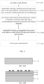
- the driver chip can be arranged on a border area of the light-emitting substrate 100, or on a side of the light-emitting substrate 100, or on a backside of the light-emitting substrate 100. The specific content will be described in the following embodiments, and will not be repeated here.
- FIG. 2 is a second structural schematic diagram of a light-emitting substrate of the present disclosure.
- the driving circuit layer 10 further includes a bonding pad 12.
- the substrate 50 is a flexible substrate, and a via hole 50 a is provided on the substrate 50.
- the via hole 50a is disposed corresponding to the bonding pad 12 and exposes a surface of each bonding pad 12 away from the cover plate 40.
- the light-emitting substrate 100 further includes at least one driver chip 60.
- the driver chip 60 includes a binding pin 61.
- the binding pin 61 is connected to the corresponding bonding pad 12 through the via hole 50a.
- the driver chip 60 can be set to 1.
- a number of driver chips 60 can be set to two or more.
- the number of driver chips 60 can be specifically set according to a size of the light-emitting substrate 100.
- the bonding pad 12 can be set in multiples.
- a number of binding pins 61 can be equal to the number of bonding pad 12.
- the bonding pads 12 are connected to the binding pins 61 in a one-to-one correspondence.
- the bonding pad 12 is bound and connected to the binding pin 61 to output the driving voltage or the power supply voltage output by the driver chip 20 to the driving circuit or the power wiring in the driving circuit layer 10.
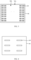
- FIG. 3 is a plane view of a light-emitting surface of a light-emitting substrate of the present disclosure.
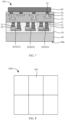
- FIG. 4 is a plane view of a backside of a light-emitting substrate of the present disclosure.
- the light-emitting substrate 100 includes a display area DA and a non-display area NA connected to the display area DA.
- the driver chip 20 is arranged in the display area DA.
- the non-display area NA is mainly provided with some wirings for transmitting signals, which will not be repeated here.
- the light-emitting substrate 100 may also only include the display area DA to achieve no border.
- the driver chip 60 is bound on the backside of the light-emitting substrate 100.
- a plurality of driver chips 60 can be provided, and the plurality of driver chips 60 can be arranged on the backside of the light-emitting substrate 100 in an array.
- the present disclosure is not limited to this, and can be specifically set according to the actual structure of the light-emitting substrate 100.
- the substrate 50 is a flexible substrate
- holes can be formed on the substrate 50 by etching technology, and then the binding of the driver chip 60 and the driving circuit layer 10 can be realized.
- the substrate 50 when the substrate50 is a PI flexible substrate, the substrate 50 can be etched with a chemical solution based on the characteristics of a PI material.
- the LED chip 20 is bound on a side of the driving circuit layer 10 close to the cover plate 40, and the driver chip 60 is bound on a side of the substrate 50 away from the cover plate 40.
- the driver chip 60 can be disposed on the backside of the light-emitting substrate 100, which saves a space for binding the driver chip 60 on the side alone, so as to achieve the purpose of reducing the borders or having no borders.
- the driver chip 60 is directly attached to the circuit board, which is less technically difficult.
- a diameter of the via hole 50 a is greater than a radial dimension of the corresponding binding pin 61. At least a portion of the binding pin 61 is disposed in the corresponding via hole 50a.
- the diameter of the via hole 50a is greater than the radial dimension of the corresponding binding pin 61.
- the binding pin 61 can be deeply inserted into the via hole 50a, thereby reducing a thickness of the light-emitting substrate 100 and improving a binding stability of the driver chip 60.
- a shape of the via hole 50a may be adapted to a shape of the binding pin 61.
- cross-sectional structures of the via hole 50a and the binding pin 61 may be rectangular or the like.
- the binding pin 61 can be fastened to the via hole 50a to further improve the binding stability of the driver chip 60.
- a length of the binding pin 61 may be greater than a depth of the via hole 50a.
- the binding pin 61 can be connected in contact with the corresponding bonding pad 12.
- a metallic bond is formed between the binding pin 61 and the corresponding bonding pad 12.
- the metallic bonds are chemical bonds that connect atoms in metals together. They differ from covalent and ionic bonds because electrons in metallic bonds are delocalized. That is, they are not shared only between two atoms. Instead, the electrons in metallic bonds float freely in a lattice of metallic nucleus. This type of bonding imparts many unique material properties to metals, including excellent thermal and electrical conductivity, and high melting point and ductility. The metallic bonding enables good electrical conductivity between the binding pin 61 and the corresponding bonding pad 12.
- FIG. 5 is a third structural schematic diagram of a light-emitting substrate of the present disclosure.
- the light-emitting substrate 100 further includes a conductive adhesive layer 70.
- the conductive adhesive layer 70 is disposed between the bonding pad 12 and the driver chip 60.
- the binding pin 61 and the corresponding bonding pad 12 are connected through the conductive adhesive layer 70.
- Material of the conductive adhesive layer 70 may be an anisotropic conductive film (ACF).
- ACF anisotropic conductive film
- the binding pin 61 and the corresponding bonding pad 12 are connected by conductive particles in the anisotropic conductive film to make them conduct. At the same time, short circuits between adjacent binding pins 61 or between adjacent bonding pads 12 can be prevented.
- the conductive adhesive layer 70 can also be made of other conductive adhesives.
- the conductive adhesive layer 70 can also be provided separately for each binding pin 61 and the corresponding bonding pad 12.
- FIG. 6 is a fourth structural schematic diagram of a light-emitting substrate of the present disclosure.
- a difference from the light-emitting substrate 100 shown in FIG. 2 is that, in the embodiment of the present disclosure, the substrate 50 is not provided in the light-emitting substrate 100.
- the driving circuit layer 10 further includes a bonding pad 12.
- the light-emitting substrate 100 further includes at least one driver chip 60.
- the driver chip 60 is disposed on the side of the driving circuit layer 10 away from the LED chip 20.
- the driver chip 60 includes a binding pin 61.
- the binding pin 61 is connected to the corresponding bonding pad 12.
- the binding pin 61 can be connected in contact with the corresponding bonding pad 12.
- a metallic bond is formed between the binding pin 61 and the corresponding bonding pad 12. That is, the binding pin 61 and the corresponding bonding pad 12 are connected through the metallic bond, so that the binding pin 61 and the corresponding bonding pad 12 have good electrical conductivity.
- the light-emitting substrate 100 provided by the embodiment of the present disclosure does not include a substrate.
- a thickness of the light-emitting substrate 100 can be further thinned to realize a thinned light-emitting substrate 100.
- the binding between each binding pin 61 and the corresponding bonding pad 12 is more convenient, and poor binding can be prevented.
- FIG. 7 is a fifth structural schematic diagram of a light-emitting substrate of the present disclosure.
- the light-emitting substrate 100 further includes a conductive adhesive layer 70.
- the conductive adhesive layer 70 is disposed between the bonding pad 12 and the driver chip 60.
- the binding pin 61 and the corresponding bonding pad 12 are connected through the conductive adhesive layer 70.
- material of the conductive adhesive layer 70 can be an anisotropic conductive film.
- the binding pin 61 and the corresponding bonding pad 12 are connected by conductive particles in the anisotropic conductive film to make them conduct. At the same time, short circuits between adjacent binding pins 61 or adjacent bonding pads 12 can be prevented.
- the conductive adhesive layer 70 can also be made of other conductive adhesives.
- the conductive adhesive layer 70 can also be provided separately for each binding pin 61 and the corresponding bonding pad 12.
- the light-emitting substrate 100 may be a display panel.
- the light-emitting substrate 100 can be a Mini-LED display panel, a Micro-LED display panel, or the like.
- the light-emitting substrate 100 may also be a backlight.
- the light-emitting substrate 100 can be used as a backlight source of a liquid crystal display device to provide the display panel with the backlight required for display.
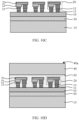
- FIG. 8 is a structural schematic diagram of a display device of the present disclosure.
- the display device 1000 is formed by splicing at least two light-emitting substrates 100.
- the light-emitting substrate 100 is the light-emitting substrate 100 described in any of the above embodiments, and details are not described herein again.
- the embodiment of the present disclosure adopts a way of binding the LED chip upside down, and the surface 40a of the cover plate away from the encapsulation layer is used as the light-emitting surface of the light-emitting substrate, that is, a light-emitting surface of display device 1000. Due to a high hardness of the cover plate, a surface scratch resistance of the light-emitting substrate can be improved, and the LED chip and the driving circuit layer can be prevented from being scratched by external substances, thereby improving the product reliability of the display device 1000.
- the driver chip can be arranged on the backside of the light-emitting substrate 100, so as to achieve the purpose of reducing the border or no border of the light-emitting substrate 100.
- the display device 1000 is formed by splicing at least two light-emitting substrates 100, a seam can be effectively reduced, and a display performance of the display device 1000 can be improved.
- FIG. 9 is a flowchart of a manufacturing method of a light-emitting substrate of the present disclosure.
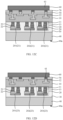
- FIG. 10A to FIG. 10E are schematic structural diagrams obtained from steps 101 to 105 in the manufacturing method of the light-emitting substrate of the present disclosure.
- the manufacturing method of the light-emitting substrate specifically includes the following steps: 101, a rigid substrate is provided.
- the rigid substrate may be a glass substrate, a resin substrate, or a rigid substrate, and configured to support.
- a substrate and a driving circuit layer are sequentially formed on the rigid substrate, and the driving circuit layer includes a binding electrode and a plurality of bonding pads.
- a substrate 50 is first deposited on the rigid substrate 15.
- the substrate 50 can be a flexible PI substrate.
- the driving circuit layer 10 may include a plurality of binding electrodes 11 and a plurality of bonding pads 12.
- the driving circuit layer 10 may include a thin film transistor functional layer disposed on the substrate 50.
- Both the binding electrode 11 and the bonding pad 12 are connected to the thin film transistor functional layer.
- the embodiment of the present disclosure adopts a glass-based MLED process, and a flat panel display process can be used to form driving transistors, that is, to form the driving circuit layer 10, so as to realize active driving.
- a connection electrode of one of the LED chips is correspondingly bound and connected to the binding electrode.
- the LED chips 20 may be Mini-LED chips, Micro-LED chips, or the like.
- the LED chip 20 further includes a luminescent material layer 23, a protective layer 22, a first electrode, and a second electrode. The first electrode and the second electrode are deposited on the luminescent material layer 12.
- Each LED chip 20 includes two connection electrodes 21. Each connection electrode 21 is connected to the first electrode or the second electrode. Alternatively, in one LED chip 20, one of the connection electrodes 21 is the first electrode, and the other connection electrode 21 is the second electrode.
- the structure of the LED chip 20 in the present disclosure is not limited to this.
- the LED chips 20 can be bound by a mass transfer technology.
- the LED chip 20 is bound in the forward direction and then applied upside down.
- COB chip on board
- a bare chip is directly attached to a circuit board
- mounting technology in the related technology, a bonding efficiency, a bonding accuracy, product specifications, etc. can be improved.
- an encapsulation layer and a cover plate are sequentially formed on a side of the LED chip away from the rigid substrate.
- an encapsulation protection adhesive is coated on a side of the LED chip 20 away from the rigid substrate 15 to form an encapsulation layer 30. Then, a cover plate 40 is attached on the encapsulation layer 30.
- Material of the encapsulation layer 30 can be OCA or other transparent adhesive.
- the encapsulation layer 30 is formed by coating with transparent adhesive, which can improve the light-emitting efficiency of the light-emitting substrate 100. Since the encapsulation layer 30 covers the LED chip 20, the LED chip 20 can be fixed and protected.
- the cover plate 40 can be a glass cover plate or other hard transparent cover plate.
- the cover plate 40 supports and protects other functional film layers in the light-emitting substrate 100. Since the surface 40a of the cover plate 40 away from the encapsulation layer 30 is the light-emitting surface of the light-emitting substrate 100, the cover plate 40 is set as a transparent cover plate, which can improve a light-emitting efficiency of the light-emitting substrate 100.
- the rigid substrate is removed.
- the light-emitting substrate formed in step 104 is inverted.
- the rigid substrate 15 is then separated from the substrate 50 using a laser lift-off technique or other processes.
- the laser lift-off technology is well known to those skilled in the art and will not be repeated here.
- the driver chip can be bound in the light-emitting substrate.
- the driver chip 20 needs to be connected to the bonding pad 12 to output the driving signal to the driving circuit layer10.
- the driver chip can be bound on a side of the light-emitting substrate, or can be bound on a backside of the driver substrate.
- FIG. 11 is a second flowchart of a manufacturing method of a light-emitting substrate of the present disclosure.
- FIG. 12A to FIG. 12D are schematic structural diagrams obtained from steps 106 to 107 in the manufacturing method of the light-emitting substrate of the present disclosure.
- a difference from the manufacturing method of the light-emitting substrate shown in FIG. 9 is that, in the embodiment of the present disclosure, the manufacturing method of the light-emitting substrate further includes the following steps: 106, a full-surface etching or a hole-forming etching is performed on the substrate to expose a surface of the bonding pad away from the cover plate.
- a full-surface of the substrate 50 is etched. That is, the substrate 50 is removed to expose the surface of the bonding pad 12 away from the cover plate 40.
- the substrate 50 is subjected to a hole-forming and etching process to form a via hole 50a.
- the via hole 50a is disposed corresponding to the bonding pad 12 to expose a surface of each bonding pad 12 away from the cover plate 40.
- a driver chip is provided, and the driver chip is bound and connected to the bonding pad.
- the driver chip 60 may include a plurality of binding pins 61.
- the bonding pads 12 can be set in multiples.
- the number of binding pins 61 can be equal to the number of bonding pads 12.
- the bonding pads 12 are connected to the binding pins 61 in a one-to-one correspondence.
- the driver chip 60 outputs the driving signal or the power supply voltage through the binding pin 61.
- the driver chip 60 is bound to the driving circuit layer 10 through the binding pin 61 and the bonding pad 12.
- each binding pin 61 is connected to the corresponding bonding pad 12 through the via hole 50a.
- a shape of the via hole 50a can be adapted to a shape of the binding pin 61.
- a diameter of the via hole 50a may also be larger than a radial dimension of the corresponding binding pin 61. At least a portion of the binding pin 61 is disposed in the corresponding via hole 50a.
- the binding pin 61 can be connected to the corresponding bonding pad 12 by using the conductive adhesive layer 70, or the connection between the binding pin 61 and the corresponding bonding pad 12 can be realized through a metallic bonding process.
- the driver chip 60 can be bound to the backside of the light-emitting substrate 100, which saves a space for binding the driver chip 60 on the side alone, so as to achieve the purpose of reducing the border or having no border.
- the driving circuit layer 10 is a thin film layer. Using the separation or half-etching of the substrate 50 and a reattachment technology of the encapsulation layer 30, both the driver chip 60 and the LED chip 20 are located on one side of the cover plate 40.
- the driver chip 60 is directly bonded to a side of the cover plate 40 including the LED chip 20.
- the driver chip 60 is connected to the bonding pad 12 by forming holes in the substrate 50 or removing the substrate 50. Compared with the related art in which the driver chip 60 is directly attached to the circuit board, the technical difficulty is smaller.
Landscapes
- Led Device Packages (AREA)
- Devices For Indicating Variable Information By Combining Individual Elements (AREA)
- Engineering & Computer Science (AREA)
- Microelectronics & Electronic Packaging (AREA)
- Manufacturing & Machinery (AREA)
Abstract
Description
- The present disclosure relates to the field of display technologies, in particular to a light-emitting substrate and a manufacturing method and a display device.
- Micro light-emitting diodes (Micro-LEDs) and sub-millimeter light-emitting diodes (Mini-LEDs) are new display technologies developed by market in recent years. These display technologies have many unparalleled advantages such as long lifespan, low image delay, wide color gamut, high refresh rate, etc. With a gradual decline in cost and maturity of related technologies, MLED (Mini-LED/Micro-LED) display device will gradually become a mainstream solution in the market. A traditional solution for forming an MLED structure is usually to first form a driving circuit and a binding electrode on a glass substrate, then transfer them directly on the glass substrate, bind LED chips, and finally apply a layer of encapsulation adhesive. Although the structure is simple, since a display surface is located on a side of the encapsulation adhesive and the driving circuit, a surface scratch resistance of the display device is weak.
- The present disclosure provides a light-emitting substrate, a manufacturing method thereof, and a display device to solve a technical problem that a surface scratch resistance of a MLED display device in the prior art is weak.
- The present disclosure provides a light-emitting substrate, including:
- a driving circuit layer including a binding electrode;
- a light-emitting diode (LED) chip including a connection electrode, where the connection electrode is connected to the binding electrode;
- an encapsulation layer disposed on a side of the LED chip away from the driving circuit layer, wherein the encapsulation layer covers the LED chip and the driving circuit layer;
- a cover plate disposed on a side of the encapsulation layer away from the LED chip, where a surface of the cover plate away from the encapsulation layer is a light-emitting surface of the light-emitting substrate.
- Alternatively, in some embodiments of the present disclosure, the light-emitting substrate further includes a substrate, and the substrate is disposed on a side of the driving circuit layer away from the LED chip.
- Alternatively, in some embodiments of the present disclosure, the driving circuit layer further includes a bonding pad, the substrate is a flexible substrate, a via hole is provided on the substrate, and the via hole is arranged corresponding to the bonding pad and exposes a surface of the bonding pad away from the cover plate; and
the light-emitting substrate further includes at least one driver chip, the driver chip includes a binding pin, and the binding pin is correspondingly connected to the bonding pad through the via hole. - Alternatively, in some embodiments of the present disclosure, a diameter of the via hole is greater than a radial dimension of the binding pin, and at least a portion of the binding pin is disposed in the via hole.
- Alternatively, in some embodiments of the present disclosure, the binding pin is fastened to the via hole.
- Alternatively, in some embodiments of the present disclosure, the driving circuit layer further includes a bonding pad, the light-emitting substrate further includes at least one driver chip, the driver chip is disposed on a side of the driving circuit layer away from the LED chip, the driver chip includes a binding pin, and the binding pin is correspondingly connected to the bonding pad.
- Alternatively, in some embodiments of the present disclosure, the binding pin is in contact with the bonding pad, and a metallic bond is formed between the binding pin and the bonding pad.
- Alternatively, in some embodiments of the present disclosure, the light-emitting substrate further includes a conductive adhesive layer, the conductive adhesive layer is disposed between the bonding pad and the driver chip, and the binding pin and the bonding pad are connected through the conductive adhesive layer.
- Alternatively, in some embodiments of the present disclosure, the light-emitting substrate is a display panel or a backlight.
- Correspondingly, the present disclosure further provides a display device. The display device is formed by splicing at least two light-emitting substrates according to any one of the above.
- Correspondingly, the present disclosure further provides a manufacturing method of a light-emitting substrate, including:
- providing a rigid substrate;
- sequentially forming a substrate and a driving circuit layer on the rigid substrate, where the driving circuit layer includes a binding electrode and a bonding pad;
- providing a plurality of light-emitting diode (LED) chips, where a connection electrode of one of the LED chips is correspondingly bound and connected to the binding electrode;
- sequentially forming an encapsulation layer and a cover plate on a side of the LED chips away from the rigid substrate;
- removing the rigid substrate.
- Alternatively, in some embodiments of the present disclosure, further including:
- performing a full-surface etching or a hole-forming etching on the substrate to expose a surface of the bonding pad away from the cover plate;
- providing a driver chip, and binding the driver chip to the bonding pad.
- The present disclosure provides the light-emitting substrate, the manufacturing method thereof, and the display device. In the light-emitting substrate, the driving circuit layer includes a plurality of binding electrodes. Each of the LED chips includes two connection electrodes. Each of the connection electrodes is connected to the corresponding binding electrode. The encapsulation layer is disposed on the side of the LED chip away from the driving circuit layer. The encapsulation layer covers the LED chip and the driving circuit layer. The cover plate is disposed on the side of the encapsulation layer away from the LED chip. The surface of the cover plate away from the encapsulation layer is the light-emitting surface of the light-emitting substrate. In the present disclosure, by binding the LED chip upside down in the light-emitting substrate, a surface scratch resistance of the light-emitting substrate can be improved, an ability of the light-emitting substrate to resist water and oxygen corrosion is improved, and a product reliability is improved. Furthermore, by removing or half-etching the substrate, the driver chip is bound to a side of the driving circuit layer away from the cover plate. A double-sided binding method is adopted, which can achieve a purpose of reducing borders or no borders.
- In order to illustrate technical solutions in the embodiments of the present disclosure more clearly, the following briefly introduces the accompanying drawings used in the description of the embodiments. Obviously, the drawings in the following description are only some implementations of the present disclosure. For example, for those skilled in the art, other drawings can also be obtained based on these drawings without any creative efforts.
-
FIG. 1 is a first structural schematic diagram of a light-emitting substrate of the present disclosure. -
FIG. 2 is a second structural schematic diagram of a light-emitting substrate of the present disclosure. -
FIG. 3 is a plane view of a light-emitting surface of a light-emitting substrate of the present disclosure. -
FIG. 4 is a plane view of a backside of a light-emitting substrate of the present disclosure. -
FIG. 5 is a third structural schematic diagram of a light-emitting substrate of the present disclosure. -
FIG. 6 is a fourth structural schematic diagram of a light-emitting substrate of the present disclosure. -
FIG. 7 is a fifth structural schematic diagram of a light-emitting substrate of the present disclosure. -
FIG. 8 is a structural schematic diagram of a display device of the present disclosure. -
FIG. 9 is a first flowchart of a manufacturing method of a light-emitting substrate of the present disclosure. -
FIG. 10A to FIG. 10E are schematic structural diagrams obtained fromsteps 101 to 105 in the manufacturing method of the light-emitting substrate of the present disclosure. -
FIG. 11 is a second flowchart of a manufacturing method of a light-emitting substrate of the present disclosure. -
FIG. 12A to FIG. 12D are schematic structural diagrams obtained fromsteps 106 to 107 in the manufacturing method of the light-emitting substrate of the present disclosure. - The following will clearly and completely describe the technical solutions in the embodiments of the present disclosure with reference to the drawings in the embodiments of the present disclosure. Obviously, the described embodiments are only a part of the embodiments of the present disclosure, but not all of them. Example. Based on the embodiments in the present disclosure, all other embodiments obtained by those skilled in the art without creative work fall within the protection scope of the present disclosure.
- In the description of the present disclosure, it should be understood that the terms "first" and "second" are used for descriptive purposes only, and should not be understood as indicating or implying relative importance or implying the number of indicated technical features. Thus, features defined as "first" and "second" etc. may expressly or implicitly include one or more of said features and are therefore not to be construed as limiting the present disclosure.
- The present disclosure provides a light-emitting substrate, a manufacturing method thereof, and a display device, which are described in detail below. It should be noted that the description order of the following embodiments is not intended to limit the preferred order of the embodiments of the present disclosure.
- Referring to
FIG. 1 , which is a first structural schematic diagram of a light-emitting substrate of the present disclosure. In an embodiment of the present disclosure, the light-emittingsubstrate 100 includes adriving circuit layer 10, a light-emitting diode (LED)chip 20, anencapsulation layer 30, and acover plate 40. The drivingcircuit layer 10 includes a bindingelectrode 11. TheLED chip 20 includes aconnection electrode 21. Theconnection electrode 21 is connected to the bindingelectrode 11. Theencapsulation layer 30 is disposed on a side of theLED chip 20 away from the drivingcircuit layer 10. Theencapsulation layer 30 covers theLED chip 20 and the drivingcircuit layer 10. Thecover plate 40 is disposed on a side of theencapsulation layer 30 away from theLED chip 20. Asurface 40a of thecover plate 40 away from theencapsulation layer 30 is a light-emitting surface of the light-emittingsubstrate 100. - In the embodiment of the present disclosure, the
LED chip 20 is bound upside down, and thesurface 40a of thecover plate 40 away from theencapsulation layer 30 is used as the light-emitting surface of the light-emittingsubstrate 100. Due to a high hardness of thecover plate 40, a scratch resistance of the surface of the light-emittingsubstrate 100 can be improved, and theLED chip 20 and the drivingcircuit layer 10 can be prevented from being scratched by external substances. In addition, in the related art, the bindingelectrode 11 and theconnection electrode 21 are disposed on the outside, exposed to theencapsulation layer 30, and easily corroded by water and oxygen. In the light-emittingsubstrate 100 of the embodiment of the present disclosure, the bindingelectrode 11 and theconnection electrode 21 are disposed inside the light-emittingsubstrate 100, which can improve the resistance of the light-emittingsubstrate 100 to water and oxygen corrosion, and improve product reliability. - In an embodiment of the present disclosure, the driving
circuit layer 10 is configured to provide theLED chip 20 with driving signals, such as a driving voltage and a power supply voltage. The drivingcircuit layer 10 may include a thin film transistor functional layer disposed on the substrate, and a specific structure of the thin film transistor functional layer may refer to the prior art, which will not be repeated here. - In the embodiment of the present disclosure, the binding
electrode 11 is used as a signal output terminal to lead out a driving signal on thedriving circuit layer 10. A number of thebinding electrodes 11 can be set to at least two, depending on the number ofLED chips 20. The bindingelectrode 11 is made of copper, aluminum, magnesium, silver, tin, indium tin oxide, and other conductive materials with good conductivity and low melting point. The bindingelectrodes 11 may be arranged in an array. The number and arrangement of thebinding electrodes 11 can be designed according to actual requirements such as a resolution of the light-emittingsubstrate 100, which is not specifically limited in the present disclosure. - In an embodiment of the present disclosure, at least two
LED chips 20 may be provided. EachLED chip 20 is provided with twoconnection electrodes 21. The drivingcircuit layer 10 is provided with twobinding electrodes 11 spaced apart corresponding to eachLED chip 20. The twobinding electrodes 11 are respectively used to lead out different driving signals in thedriving circuit layer 10. Eachconnection electrode 21 and the correspondingbinding electrode 11 can be connected by asolder paste 13, or may also be directly connected through fusion welding, metallic bonds, etc., which is not specifically limited in the present disclosure. - In an embodiment of the present disclosure, the LED chips 20 may be Mini-LED chips, Micro-LED chips, or the like. A number of
LED chips 20 can be set according to requirements such as a size of the light-emittingsubstrate 100 and a luminous brightness. TheLED chip 20 further includes aluminescent material layer 23, aprotective layer 22, a first electrode, and a second electrode. The first electrode and the second electrode are deposited on theluminescent material layer 23. Eachconnection electrode 21 is connected to the first electrode or the second electrode. Alternatively, in oneLED chip 20, one of theconnection electrodes 21 is the first electrode, and theother connection electrode 21 is the second electrode. Apparently, the structure of theLED chip 20 in the present disclosure is not limited to this. - A light-emitting material of the
LED chip 20 may be an inorganic light-emitting material such as gallium nitride or an organic light-emitting material such as quantum dots. TheLED chip 20 can emit red light, blue light, green light, white light, yellow light, and the like. When manufacturing theLED chip 20, different luminescent materials can be selected according to different luminous color requirements. - In an embodiment of the present disclosure, the plurality of
LED chips 20 include a red LED chip, a green LED chip, and a blue LED chip. In the red LED chip, theluminescent material layer 23 is a redluminescent material layer 201. In the green LED chip, theluminescent material layer 23 is a greenluminescent material layer 202. In the blue LED chip, theluminescent material layer 23 is a blueluminescent material layer 203. - In the embodiment of the present disclosure, material of the
encapsulation layer 30 is generally transparent to improve a light transmittance of the light-emittingsubstrate 100. Specifically, the material of theencapsulation layer 30 may be an optically clear adhesive (OCA) or other transparent adhesives. In the embodiments of the present disclosure, the optically clear adhesive is used to form theencapsulation layer 30, on the one hand, it can improve a light-emitting efficiency of the light-emittingsubstrate 100. On the other hand, an adhesive force between the drivingcircuit layer 10 and thecover plate 40 can be improved, and a structural stability of the light-emittingsubstrate 100 can be improved. In a third aspect, since theencapsulation layer 30 covers theLED chip 20, theLED chip 20 can be fixed and protected. - In an embodiment of the present disclosure, the
cover plate 40 may be a glass cover plate or other hard transparent cover plate. Thecover plate 40 supports and protects other functional film layers in the light-emittingsubstrate 100. Since thesurface 40a of thecover plate 40 away from theencapsulation layer 30 is the light-emitting surface of the light-emittingsubstrate 100, thecover plate 40 is set as a transparent cover plate, which can improve a light-emitting efficiency of the light-emittingsubstrate 100. - In one embodiment of the present disclosure, the light-emitting
substrate 100 further includes asubstrate 50. Thesubstrate 50 is disposed on a side of the drivingcircuit layer 10 away from theLED chip 20. - The
substrate 50 can be a flexible substrate or a rigid substrate. Thesubstrate 50 may include one or more than two layers of flexible polyimide (PI). Thesubstrate 50 can also be made of resin or the like. - In the embodiment of the present disclosure, the
substrate 50 is disposed on the side of the drivingcircuit layer 10 away from theLED chip 20, which can protect and support the drivingcircuit layer 10 and improve the structural stability of the light-emittingsubstrate 100. - In an embodiment of the present disclosure, the light-emitting
substrate 100 may further include a driver chip. The driver chip is used to provide driving signals or power voltages to thedriving circuit layer 10. The driver chip can be arranged on a border area of the light-emittingsubstrate 100, or on a side of the light-emittingsubstrate 100, or on a backside of the light-emittingsubstrate 100. The specific content will be described in the following embodiments, and will not be repeated here. - Referring to
FIG. 2, FIG. 2 is a second structural schematic diagram of a light-emitting substrate of the present disclosure. A difference from the light-emittingsubstrate 100 described inFIG. 1 is that, in an embodiment of the present disclosure, the drivingcircuit layer 10 further includes abonding pad 12. Thesubstrate 50 is a flexible substrate, and a viahole 50 a is provided on thesubstrate 50. The viahole 50a is disposed corresponding to thebonding pad 12 and exposes a surface of eachbonding pad 12 away from thecover plate 40. - The light-emitting
substrate 100 further includes at least onedriver chip 60. Thedriver chip 60 includes abinding pin 61. The bindingpin 61 is connected to thecorresponding bonding pad 12 through the viahole 50a. - The
driver chip 60 can be set to 1. A number ofdriver chips 60 can be set to two or more. The number ofdriver chips 60 can be specifically set according to a size of the light-emittingsubstrate 100. Thebonding pad 12 can be set in multiples. A number ofbinding pins 61 can be equal to the number ofbonding pad 12. Thebonding pads 12 are connected to the bindingpins 61 in a one-to-one correspondence. - The
bonding pad 12 is bound and connected to thebinding pin 61 to output the driving voltage or the power supply voltage output by thedriver chip 20 to the driving circuit or the power wiring in thedriving circuit layer 10. - Specifically, refer to
FIG. 3 and FIG. 4. FIG. 3 is a plane view of a light-emitting surface of a light-emitting substrate of the present disclosure.FIG. 4 is a plane view of a backside of a light-emitting substrate of the present disclosure. As shown inFIG. 3 , the light-emittingsubstrate 100 includes a display area DA and a non-display area NA connected to the display area DA. Thedriver chip 20 is arranged in the display area DA. The non-display area NA is mainly provided with some wirings for transmitting signals, which will not be repeated here. Apparently, in some embodiments, the light-emittingsubstrate 100 may also only include the display area DA to achieve no border. Thedriver chip 60 is bound on the backside of the light-emittingsubstrate 100. A plurality ofdriver chips 60 can be provided, and the plurality ofdriver chips 60 can be arranged on the backside of the light-emittingsubstrate 100 in an array. Apparently, regarding the setting of the driver chips 60, the present disclosure is not limited to this, and can be specifically set according to the actual structure of the light-emittingsubstrate 100. - In the embodiment of the present disclosure, since the
substrate 50 is a flexible substrate, holes can be formed on thesubstrate 50 by etching technology, and then the binding of thedriver chip 60 and the drivingcircuit layer 10 can be realized. For example, when the substrate50 is a PI flexible substrate, thesubstrate 50 can be etched with a chemical solution based on the characteristics of a PI material. - In the embodiment of the present disclosure, the
LED chip 20 is bound on a side of the drivingcircuit layer 10 close to thecover plate 40, and thedriver chip 60 is bound on a side of thesubstrate 50 away from thecover plate 40. By using a double-sided bonding technology and the etching technology of thesubstrate 50, thedriver chip 60 can be disposed on the backside of the light-emittingsubstrate 100, which saves a space for binding thedriver chip 60 on the side alone, so as to achieve the purpose of reducing the borders or having no borders. In addition, compared with the related art, thedriver chip 60 is directly attached to the circuit board, which is less technically difficult. - Referring to
FIG. 2 , in the embodiment of the present disclosure, a diameter of the viahole 50 a is greater than a radial dimension of the correspondingbinding pin 61. At least a portion of thebinding pin 61 is disposed in the corresponding viahole 50a. - In the embodiment of the present disclosure, the diameter of the via
hole 50a is greater than the radial dimension of the correspondingbinding pin 61. When binding thedriver chip 60, the bindingpin 61 can be deeply inserted into the viahole 50a, thereby reducing a thickness of the light-emittingsubstrate 100 and improving a binding stability of thedriver chip 60. - In an embodiment of the present disclosure, a shape of the via
hole 50a may be adapted to a shape of thebinding pin 61. For example, cross-sectional structures of the viahole 50a and thebinding pin 61 may be rectangular or the like. The bindingpin 61 can be fastened to the viahole 50a to further improve the binding stability of thedriver chip 60. - In an embodiment of the present disclosure, a length of the
binding pin 61 may be greater than a depth of the viahole 50a. In this case, the bindingpin 61 can be connected in contact with thecorresponding bonding pad 12. A metallic bond is formed between thebinding pin 61 and thecorresponding bonding pad 12. - The metallic bonds are chemical bonds that connect atoms in metals together. They differ from covalent and ionic bonds because electrons in metallic bonds are delocalized. That is, they are not shared only between two atoms. Instead, the electrons in metallic bonds float freely in a lattice of metallic nucleus. This type of bonding imparts many unique material properties to metals, including excellent thermal and electrical conductivity, and high melting point and ductility. The metallic bonding enables good electrical conductivity between the
binding pin 61 and thecorresponding bonding pad 12. - Referring to
FIG. 5, FIG. 5 is a third structural schematic diagram of a light-emitting substrate of the present disclosure. A difference from the light-emittingsubstrate 100 shown inFIG. 2 is that, in the embodiment of the present disclosure, the light-emittingsubstrate 100 further includes a conductiveadhesive layer 70. The conductiveadhesive layer 70 is disposed between thebonding pad 12 and thedriver chip 60. The bindingpin 61 and thecorresponding bonding pad 12 are connected through the conductiveadhesive layer 70. - Material of the conductive
adhesive layer 70 may be an anisotropic conductive film (ACF). The bindingpin 61 and thecorresponding bonding pad 12 are connected by conductive particles in the anisotropic conductive film to make them conduct. At the same time, short circuits between adjacentbinding pins 61 or betweenadjacent bonding pads 12 can be prevented. Apparently, the conductiveadhesive layer 70 can also be made of other conductive adhesives. The conductiveadhesive layer 70 can also be provided separately for eachbinding pin 61 and thecorresponding bonding pad 12. - Referring to
FIG. 6 , which is a fourth structural schematic diagram of a light-emitting substrate of the present disclosure. A difference from the light-emittingsubstrate 100 shown inFIG. 2 is that, in the embodiment of the present disclosure, thesubstrate 50 is not provided in the light-emittingsubstrate 100. - Similarly, in the embodiment of the present disclosure, the driving
circuit layer 10 further includes abonding pad 12. The light-emittingsubstrate 100 further includes at least onedriver chip 60. Thedriver chip 60 is disposed on the side of the drivingcircuit layer 10 away from theLED chip 20. Thedriver chip 60 includes abinding pin 61. The bindingpin 61 is connected to thecorresponding bonding pad 12. - The binding
pin 61 can be connected in contact with thecorresponding bonding pad 12. A metallic bond is formed between thebinding pin 61 and thecorresponding bonding pad 12. That is, the bindingpin 61 and thecorresponding bonding pad 12 are connected through the metallic bond, so that the bindingpin 61 and thecorresponding bonding pad 12 have good electrical conductivity. - The light-emitting
substrate 100 provided by the embodiment of the present disclosure does not include a substrate. On the one hand, a thickness of the light-emittingsubstrate 100 can be further thinned to realize a thinned light-emittingsubstrate 100. On the other hand, the binding between eachbinding pin 61 and thecorresponding bonding pad 12 is more convenient, and poor binding can be prevented. - Referring to
FIG. 7 , which is a fifth structural schematic diagram of a light-emitting substrate of the present disclosure. A difference from the light-emittingsubstrate 100 shown inFIG. 6 is that, in the embodiment of the present disclosure, the light-emittingsubstrate 100 further includes a conductiveadhesive layer 70. The conductiveadhesive layer 70 is disposed between thebonding pad 12 and thedriver chip 60. The bindingpin 61 and thecorresponding bonding pad 12 are connected through the conductiveadhesive layer 70. - Similarly, material of the conductive
adhesive layer 70 can be an anisotropic conductive film. The bindingpin 61 and thecorresponding bonding pad 12 are connected by conductive particles in the anisotropic conductive film to make them conduct. At the same time, short circuits between adjacentbinding pins 61 oradjacent bonding pads 12 can be prevented. Apparently, the conductiveadhesive layer 70 can also be made of other conductive adhesives. The conductiveadhesive layer 70 can also be provided separately for eachbinding pin 61 and thecorresponding bonding pad 12. - In some embodiments of the present disclosure, the light-emitting
substrate 100 may be a display panel. For example, the light-emittingsubstrate 100 can be a Mini-LED display panel, a Micro-LED display panel, or the like. In some embodiments of the present disclosure, the light-emittingsubstrate 100 may also be a backlight. For example, the light-emittingsubstrate 100 can be used as a backlight source of a liquid crystal display device to provide the display panel with the backlight required for display. - Correspondingly, refer to
FIG. 8 , which is a structural schematic diagram of a display device of the present disclosure. In the embodiment of the present disclosure, thedisplay device 1000 is formed by splicing at least two light-emittingsubstrates 100. The light-emittingsubstrate 100 is the light-emittingsubstrate 100 described in any of the above embodiments, and details are not described herein again. - In the
display device 1000, the embodiment of the present disclosure adopts a way of binding the LED chip upside down, and thesurface 40a of the cover plate away from the encapsulation layer is used as the light-emitting surface of the light-emitting substrate, that is, a light-emitting surface ofdisplay device 1000. Due to a high hardness of the cover plate, a surface scratch resistance of the light-emitting substrate can be improved, and the LED chip and the driving circuit layer can be prevented from being scratched by external substances, thereby improving the product reliability of thedisplay device 1000. - In addition, in some embodiments of the present disclosure, by using double-sided bonding and substrate etching technologies, the driver chip can be arranged on the backside of the light-emitting
substrate 100, so as to achieve the purpose of reducing the border or no border of the light-emittingsubstrate 100. When thedisplay device 1000 is formed by splicing at least two light-emittingsubstrates 100, a seam can be effectively reduced, and a display performance of thedisplay device 1000 can be improved. - Correspondingly, the present disclosure also provides a manufacturing method of a light-emitting substrate. Referring to
FIG. 9 and FIG. 10A toFIG. 10E for details.FIG. 9 is a flowchart of a manufacturing method of a light-emitting substrate of the present disclosure.FIG. 10A to FIG. 10E are schematic structural diagrams obtained fromsteps 101 to 105 in the manufacturing method of the light-emitting substrate of the present disclosure. The manufacturing method of the light-emitting substrate specifically includes the following steps:
101, a rigid substrate is provided. - As shown in
FIG. 10A , the rigid substrate may be a glass substrate, a resin substrate, or a rigid substrate, and configured to support. - 102, a substrate and a driving circuit layer are sequentially formed on the rigid substrate, and the driving circuit layer includes a binding electrode and a plurality of bonding pads.
- As shown in
FIG. 10B , asubstrate 50 is first deposited on therigid substrate 15. Thesubstrate 50 can be a flexible PI substrate. - Then, a driving
circuit layer 10 is formed on thesubstrate 50. The drivingcircuit layer 10 may include a plurality ofbinding electrodes 11 and a plurality ofbonding pads 12. The drivingcircuit layer 10 may include a thin film transistor functional layer disposed on thesubstrate 50. For the specific structure of the functional layer of the thin film transistor, reference may be made to the prior art, which will not be repeated here. Both the bindingelectrode 11 and thebonding pad 12 are connected to the thin film transistor functional layer. - The embodiment of the present disclosure adopts a glass-based MLED process, and a flat panel display process can be used to form driving transistors, that is, to form the
driving circuit layer 10, so as to realize active driving. - 103, a plurality of LED chips are provided, and a connection electrode of one of the LED chips is correspondingly bound and connected to the binding electrode.
- As shown in
FIG. 10C , the LED chips 20 may be Mini-LED chips, Micro-LED chips, or the like. TheLED chip 20 further includes aluminescent material layer 23, aprotective layer 22, a first electrode, and a second electrode. The first electrode and the second electrode are deposited on theluminescent material layer 12. EachLED chip 20 includes twoconnection electrodes 21. Eachconnection electrode 21 is connected to the first electrode or the second electrode. Alternatively, in oneLED chip 20, one of theconnection electrodes 21 is the first electrode, and theother connection electrode 21 is the second electrode. Apparently, the structure of theLED chip 20 in the present disclosure is not limited to this. - Specifically, in the embodiment of the present disclosure, the LED chips 20 can be bound by a mass transfer technology. The
LED chip 20 is bound in the forward direction and then applied upside down. Compared with a chip on board (COB, a bare chip is directly attached to a circuit board)/mounting technology in the related technology, a bonding efficiency, a bonding accuracy, product specifications, etc. can be improved. - 104, an encapsulation layer and a cover plate are sequentially formed on a side of the LED chip away from the rigid substrate.
- As shown in
FIG. 10D , an encapsulation protection adhesive is coated on a side of theLED chip 20 away from therigid substrate 15 to form anencapsulation layer 30. Then, acover plate 40 is attached on theencapsulation layer 30. - Material of the
encapsulation layer 30 can be OCA or other transparent adhesive. Theencapsulation layer 30 is formed by coating with transparent adhesive, which can improve the light-emitting efficiency of the light-emittingsubstrate 100. Since theencapsulation layer 30 covers theLED chip 20, theLED chip 20 can be fixed and protected. - The
cover plate 40 can be a glass cover plate or other hard transparent cover plate. Thecover plate 40 supports and protects other functional film layers in the light-emittingsubstrate 100. Since thesurface 40a of thecover plate 40 away from theencapsulation layer 30 is the light-emitting surface of the light-emittingsubstrate 100, thecover plate 40 is set as a transparent cover plate, which can improve a light-emitting efficiency of the light-emittingsubstrate 100. - 105, the rigid substrate is removed.
- As shown in
FIG. 10E , the light-emitting substrate formed instep 104 is inverted. Therigid substrate 15 is then separated from thesubstrate 50 using a laser lift-off technique or other processes. The laser lift-off technology is well known to those skilled in the art and will not be repeated here. - Furthermore, the driver chip can be bound in the light-emitting substrate. The
driver chip 20 needs to be connected to thebonding pad 12 to output the driving signal to the driving circuit layer10. The driver chip can be bound on a side of the light-emitting substrate, or can be bound on a backside of the driver substrate. - Specifically, refer to
FIG. 11 andFIG. 12A toFIG. 12D .FIG. 11 is a second flowchart of a manufacturing method of a light-emitting substrate of the present disclosure.FIG. 12A to FIG. 12D are schematic structural diagrams obtained fromsteps 106 to 107 in the manufacturing method of the light-emitting substrate of the present disclosure. A difference from the manufacturing method of the light-emitting substrate shown inFIG. 9 is that, in the embodiment of the present disclosure, the manufacturing method of the light-emitting substrate further includes the following steps:
106, a full-surface etching or a hole-forming etching is performed on the substrate to expose a surface of the bonding pad away from the cover plate. - In some embodiments, as shown in
FIG. 12A , a full-surface of thesubstrate 50 is etched. That is, thesubstrate 50 is removed to expose the surface of thebonding pad 12 away from thecover plate 40. - In other embodiments, as shown in
FIG. 12B , thesubstrate 50 is subjected to a hole-forming and etching process to form a viahole 50a. The viahole 50a is disposed corresponding to thebonding pad 12 to expose a surface of eachbonding pad 12 away from thecover plate 40. - 107, a driver chip is provided, and the driver chip is bound and connected to the bonding pad.
- Specifically, the
driver chip 60 may include a plurality of binding pins 61. Thebonding pads 12 can be set in multiples. The number ofbinding pins 61 can be equal to the number ofbonding pads 12. Thebonding pads 12 are connected to the bindingpins 61 in a one-to-one correspondence. Thedriver chip 60 outputs the driving signal or the power supply voltage through the bindingpin 61. - In some embodiments, as shown in
FIG. 12C , after the entire surface of thesubstrate 50 is etched, thedriver chip 60 is bound to thedriving circuit layer 10 through the bindingpin 61 and thebonding pad 12. - In other embodiments, as shown in
FIG. 12D , after thesubstrate 50 is formed with holes and etched, each bindingpin 61 is connected to thecorresponding bonding pad 12 through the viahole 50a. - A shape of the via
hole 50a can be adapted to a shape of thebinding pin 61. A diameter of the viahole 50a may also be larger than a radial dimension of the correspondingbinding pin 61. At least a portion of thebinding pin 61 is disposed in the corresponding viahole 50a. - In the embodiment of the present disclosure, the binding
pin 61 can be connected to thecorresponding bonding pad 12 by using the conductiveadhesive layer 70, or the connection between thebinding pin 61 and thecorresponding bonding pad 12 can be realized through a metallic bonding process. - In the manufacturing method of the light-emitting substrate provided in the embodiments of the present disclosure, by etching the
substrate 50 to form holes or etch the entire surface, thedriver chip 60 can be bound to the backside of the light-emittingsubstrate 100, which saves a space for binding thedriver chip 60 on the side alone, so as to achieve the purpose of reducing the border or having no border. In addition, in the embodiments of the present disclosure, the drivingcircuit layer 10 is a thin film layer. Using the separation or half-etching of thesubstrate 50 and a reattachment technology of theencapsulation layer 30, both thedriver chip 60 and theLED chip 20 are located on one side of thecover plate 40. Moreover, in the embodiment of the present disclosure, thedriver chip 60 is directly bonded to a side of thecover plate 40 including theLED chip 20. Thedriver chip 60 is connected to thebonding pad 12 by forming holes in thesubstrate 50 or removing thesubstrate 50. Compared with the related art in which thedriver chip 60 is directly attached to the circuit board, the technical difficulty is smaller. - The light-emitting substrate, the manufacturing method thereof, and the display device provided by the present disclosure are introduced in detail above. In this specification, specific embodiments are used to illustrate the principles and implementations of the present disclosure. The descriptions of the above embodiments are only used to help understand the method and the core idea of the present disclosure; meanwhile, for those skilled in the art, according to the idea of the present disclosure, there will be changes in the specific implementation and application scope. In conclusion, the content of this specification should not be construed as a limitation on the present disclosure.
Claims (20)
- A light-emitting substrate, comprising:a driving circuit layer comprising a binding electrode;a light-emitting diode (LED) chip comprising a connection electrode, wherein the connection electrode is connected to the binding electrode;an encapsulation layer disposed on a side of the LED chip away from the driving circuit layer, wherein the encapsulation layer covers the LED chip and the driving circuit layer; anda cover plate disposed on a side of the encapsulation layer away from the LED chip, wherein a surface of the cover plate away from the encapsulation layer is a light-emitting surface of the light-emitting substrate.
- The light-emitting substrate according to claim 1, wherein the light-emitting substrate further comprises a substrate, and the substrate is disposed on a side of the driving circuit layer away from the LED chip.
- The light-emitting substrate according to claim 2, wherein the driving circuit layer further comprises a bonding pad, the substrate is a flexible substrate, a via hole is provided on the substrate, and the via hole is arranged corresponding to the bonding pad and exposes a surface of the bonding pad away from the cover plate; and
the light-emitting substrate further comprises at least one driver chip, the driver chip comprises a binding pin, and the binding pin is correspondingly connected to the bonding pad through the via hole. - The light-emitting substrate according to claim 3, wherein a diameter of the via hole is greater than a radial dimension of the binding pin, and at least a portion of the binding pin is disposed in the via hole.
- The light-emitting substrate according to claim 3, wherein the binding pin is fastened to the via hole.
- The light-emitting substrate according to claim 1, wherein the driving circuit layer further comprises a bonding pad, the light-emitting substrate further comprises at least one driver chip, the driver chip is disposed on a side of the driving circuit layer away from the LED chip, the driver chip comprises a binding pin, and the binding pin is correspondingly connected to the bonding pad.
- The light-emitting substrate according to claim 3, wherein the binding pin is in contact with the bonding pad, and a metallic bond is formed between the binding pin and the bonding pad.
- The light-emitting substrate according to claim 3, wherein the light-emitting substrate further comprises a conductive adhesive layer, the conductive adhesive layer is disposed between the bonding pad and the driver chip, and the binding pin and the bonding pad are connected through the conductive adhesive layer.
- The light-emitting substrate according to claim 1, wherein the light-emitting substrate is a display panel or a backlight.
- A display device, wherein the display device is formed by splicing at least two light-emitting substrates according to claim 1.
- The display device according to claim 10, wherein the light-emitting substrate further comprises a substrate, and the substrate is disposed on a side of the driving circuit layer away from the LED chip.
- The display device according to claim 11, wherein the driving circuit layer further comprises a bonding pad, the substrate is a flexible substrate, a via hole is provided on the substrate, and the via hole is arranged corresponding to the bonding pad and exposes a surface of the bonding pad away from the cover plate; and
the light-emitting substrate further comprises at least one driver chip, the driver chip comprises a binding pin, and the binding pin is correspondingly connected to the bonding pad through the via hole. - The display device according to claim 12, wherein a diameter of the via hole is greater than a radial dimension of the binding pin, and at least a portion of the binding pin is disposed in the via hole.
- The display device according to claim 12, wherein the binding pin is fastened to the via hole.
- The display device according to claim 10, wherein the driving circuit layer further comprises a bonding pad, the light-emitting substrate further comprises at least one driver chip, the driver chip is disposed on a side of the driving circuit layer away from the LED chip, the driver chip comprises a binding pin, and the binding pin is correspondingly connected to the bonding pad.
- The display device according to claim 12, wherein the binding pin is in contact with the bonding pad, and a metallic bond is formed between the binding pin and the bonding pad.
- The display device according to claim 12, wherein the light-emitting substrate further comprises a conductive adhesive layer, the conductive adhesive layer is disposed between the bonding pad and the driver chip, and the binding pin and the bonding pad are connected through the conductive adhesive layer.
- The display device according to claim 10, wherein the light-emitting substrate is a display panel or a backlight.
- A manufacturing method of a light-emitting substrate, comprising:providing a rigid substrate;sequentially forming a substrate and a driving circuit layer on the rigid substrate, wherein the driving circuit layer comprises a binding electrode and a bonding pad;providing a plurality of light-emitting diode (LED) chips, wherein a connection electrode of one of the LED chips is correspondingly bound and connected to the binding electrode;sequentially forming an encapsulation layer and a cover plate on a side of the LED chips away from the rigid substrate; andremoving the rigid substrate.
- The manufacturing method of the light-emitting substrate according to claim 19, further comprising:performing a full-surface etching or a hole-forming etching on the substrate to expose a surface of the bonding pad away from the cover plate; andproviding a driver chip, and binding the driver chip to the bonding pad.
Applications Claiming Priority (2)
| Application Number | Priority Date | Filing Date | Title |
|---|---|---|---|
| CN202210751104.0A CN115117225A (en) | 2022-06-28 | 2022-06-28 | Light-emitting substrate, manufacturing method thereof and display device |
| PCT/CN2022/105166 WO2024000647A1 (en) | 2022-06-28 | 2022-07-12 | Light-emitting substrate and fabrication method therefor, and display apparatus |
Publications (1)
| Publication Number | Publication Date |
|---|---|
| EP4550429A1 true EP4550429A1 (en) | 2025-05-07 |
Family
ID=89323489
Family Applications (1)
| Application Number | Title | Priority Date | Filing Date |
|---|---|---|---|
| EP22741416.6A Pending EP4550429A1 (en) | 2022-06-28 | 2022-07-12 | Light-emitting substrate and fabrication method therefor, and display apparatus |
Country Status (4)
| Country | Link |
|---|---|
| US (1) | US12489099B2 (en) |
| EP (1) | EP4550429A1 (en) |
| JP (1) | JP7625609B2 (en) |
| KR (1) | KR20240003434A (en) |
Cited By (1)
| Publication number | Priority date | Publication date | Assignee | Title |
|---|---|---|---|---|
| CN120435143A (en) * | 2025-07-08 | 2025-08-05 | 杭州芯聚半导体有限公司 | A MicroLED device with a strip-shaped LED light source and a manufacturing method thereof |
Families Citing this family (1)
| Publication number | Priority date | Publication date | Assignee | Title |
|---|---|---|---|---|
| CN118575278A (en) * | 2022-07-19 | 2024-08-30 | 京东方科技集团股份有限公司 | Light-emitting substrate, manufacturing method thereof and display panel |
Family Cites Families (12)
| Publication number | Priority date | Publication date | Assignee | Title |
|---|---|---|---|---|
| JP2014218434A (en) | 2013-04-30 | 2014-11-20 | キヤノン株式会社 | New organic compound, organic light-emitting element and image display device |
| KR102049735B1 (en) | 2013-04-30 | 2019-11-28 | 엘지디스플레이 주식회사 | Organic Light Emitting Diode Display Device and Method for Manufacturing The Same |
| US10665578B2 (en) * | 2015-09-24 | 2020-05-26 | Apple Inc. | Display with embedded pixel driver chips |
| CN107564928B (en) | 2016-06-30 | 2020-04-14 | 群创光电股份有限公司 | Display device |
| KR102498252B1 (en) | 2017-09-26 | 2023-02-10 | 삼성전자주식회사 | Display including luminous chips and manufacturing method thereof |
| TWI680593B (en) * | 2018-10-12 | 2019-12-21 | 欣興電子股份有限公司 | Light emitting device package structure and manufacturing method thereof |
| CN109904186B (en) | 2019-02-28 | 2021-10-29 | 京东方科技集团股份有限公司 | A display substrate, its manufacturing method, and a display device |
| CN109904080B (en) | 2019-03-20 | 2020-10-02 | 北京京东方显示技术有限公司 | Driving backboard, manufacturing method thereof and display device |
| KR102739953B1 (en) | 2019-10-22 | 2024-12-06 | 삼성전자주식회사 | Micro LED device and method for manufacturing the same |
| TWI711192B (en) * | 2020-04-21 | 2020-11-21 | 欣興電子股份有限公司 | Light emitting diode package structure and manufacturing method thereof |
| CN111769108A (en) | 2020-06-30 | 2020-10-13 | 上海天马微电子有限公司 | Display panel, method for producing the same, and display device |
| CN114664745B (en) | 2022-05-24 | 2023-01-17 | 惠科股份有限公司 | Display panel and manufacturing method thereof |
-
2022
- 2022-07-12 KR KR1020237014417A patent/KR20240003434A/en active Pending
- 2022-07-12 US US17/793,722 patent/US12489099B2/en active Active
- 2022-07-12 EP EP22741416.6A patent/EP4550429A1/en active Pending
- 2022-07-12 JP JP2022546048A patent/JP7625609B2/en active Active
Cited By (1)
| Publication number | Priority date | Publication date | Assignee | Title |
|---|---|---|---|---|
| CN120435143A (en) * | 2025-07-08 | 2025-08-05 | 杭州芯聚半导体有限公司 | A MicroLED device with a strip-shaped LED light source and a manufacturing method thereof |
Also Published As
| Publication number | Publication date |
|---|---|
| JP2024529801A (en) | 2024-08-14 |
| US20230420431A1 (en) | 2023-12-28 |
| JP7625609B2 (en) | 2025-02-03 |
| US12489099B2 (en) | 2025-12-02 |
| KR20240003434A (en) | 2024-01-09 |
Similar Documents
| Publication | Publication Date | Title |
|---|---|---|
| CN110164901B (en) | Array substrate and preparation method thereof, display panel and display device | |
| CN111261057B (en) | Display panel and display device | |
| CN113644181A (en) | Light-emitting substrate, method for manufacturing the same, and display device | |
| US11415843B2 (en) | Display panel and liquid crystal display device | |
| CN111276474B (en) | Display panels and display devices | |
| WO2024000647A1 (en) | Light-emitting substrate and fabrication method therefor, and display apparatus | |
| US12489099B2 (en) | Light-emitting substrate, manufacturing method thereof, and display device | |
| CN110277365B (en) | Electronic devices and splicing electronic systems | |
| CN109686719B (en) | Electronic device and display equipment comprising same | |
| CN111781772A (en) | LED backlight source, LED backlight module and preparation method | |
| TWM268600U (en) | Structure of chip on glass and liquid crystal display device using the structure | |
| CN116053270A (en) | Display panel and splicing display module | |
| CN115132813A (en) | Display module and preparation method thereof | |
| CN116941335A (en) | Circuit board, preparation method thereof and functional backboard | |
| CN116190499B (en) | Display panel, preparation method thereof and display device | |
| WO2023005610A1 (en) | Drive substrate and preparation method therefor, and light-emitting apparatus | |
| CN114868077B (en) | Driving backplane and preparation method thereof and display module | |
| WO2024044912A1 (en) | Wiring substrate and manufacturing method therefor, and light-emitting substrate and display apparatus | |
| CN117457613A (en) | Display panel, display panel manufacturing method and electronic device | |
| KR20070051619A (en) | OID display device capable of bidirectional display | |
| US20260020405A1 (en) | Micro light-emitting diode substrate and manufacturing method thereof | |
| US12457005B2 (en) | Manufacturing method of electronic device | |
| CN115832001B (en) | Display module, preparation method and spliced display screen | |
| CN220087561U (en) | Circuit board, backlight module and display device | |
| WO2023159419A1 (en) | Array substrate and display device |
Legal Events
| Date | Code | Title | Description |
|---|---|---|---|
| STAA | Information on the status of an ep patent application or granted ep patent |
Free format text: STATUS: UNKNOWN |
|
| STAA | Information on the status of an ep patent application or granted ep patent |
Free format text: STATUS: THE INTERNATIONAL PUBLICATION HAS BEEN MADE |
|
| PUAI | Public reference made under article 153(3) epc to a published international application that has entered the european phase |
Free format text: ORIGINAL CODE: 0009012 |
|
| STAA | Information on the status of an ep patent application or granted ep patent |
Free format text: STATUS: REQUEST FOR EXAMINATION WAS MADE |
|
| 17P | Request for examination filed |
Effective date: 20220728 |
|
| AK | Designated contracting states |
Kind code of ref document: A1 Designated state(s): AL AT BE BG CH CY CZ DE DK EE ES FI FR GB GR HR HU IE IS IT LI LT LU LV MC MK MT NL NO PL PT RO RS SE SI SK SM TR |
|
| DAV | Request for validation of the european patent (deleted) | ||
| DAX | Request for extension of the european patent (deleted) | ||
| REG | Reference to a national code |
Ref country code: DE Ref legal event code: R079 Free format text: PREVIOUS MAIN CLASS: H01L0033620000 Ipc: H10H0029010000 |