EP4550427A1 - Photodetector - Google Patents
Photodetector Download PDFInfo
- Publication number
- EP4550427A1 EP4550427A1 EP22949448.9A EP22949448A EP4550427A1 EP 4550427 A1 EP4550427 A1 EP 4550427A1 EP 22949448 A EP22949448 A EP 22949448A EP 4550427 A1 EP4550427 A1 EP 4550427A1
- Authority
- EP
- European Patent Office
- Prior art keywords
- photodiode
- layer
- protection diode
- semiconductor portion
- type
- Prior art date
- Legal status (The legal status is an assumption and is not a legal conclusion. Google has not performed a legal analysis and makes no representation as to the accuracy of the status listed.)
- Pending
Links
Images



Classifications
-
- H—ELECTRICITY
- H10—SEMICONDUCTOR DEVICES; ELECTRIC SOLID-STATE DEVICES NOT OTHERWISE PROVIDED FOR
- H10F—INORGANIC SEMICONDUCTOR DEVICES SENSITIVE TO INFRARED RADIATION, LIGHT, ELECTROMAGNETIC RADIATION OF SHORTER WAVELENGTH OR CORPUSCULAR RADIATION
- H10F30/00—Individual radiation-sensitive semiconductor devices in which radiation controls the flow of current through the devices, e.g. photodetectors
- H10F30/20—Individual radiation-sensitive semiconductor devices in which radiation controls the flow of current through the devices, e.g. photodetectors the devices having potential barriers, e.g. phototransistors
- H10F30/21—Individual radiation-sensitive semiconductor devices in which radiation controls the flow of current through the devices, e.g. photodetectors the devices having potential barriers, e.g. phototransistors the devices being sensitive to infrared, visible or ultraviolet radiation
- H10F30/22—Individual radiation-sensitive semiconductor devices in which radiation controls the flow of current through the devices, e.g. photodetectors the devices having potential barriers, e.g. phototransistors the devices being sensitive to infrared, visible or ultraviolet radiation the devices having only one potential barrier, e.g. photodiodes
- H10F30/223—Individual radiation-sensitive semiconductor devices in which radiation controls the flow of current through the devices, e.g. photodetectors the devices having potential barriers, e.g. phototransistors the devices being sensitive to infrared, visible or ultraviolet radiation the devices having only one potential barrier, e.g. photodiodes the potential barrier being a PIN barrier
-
- H—ELECTRICITY
- H10—SEMICONDUCTOR DEVICES; ELECTRIC SOLID-STATE DEVICES NOT OTHERWISE PROVIDED FOR
- H10F—INORGANIC SEMICONDUCTOR DEVICES SENSITIVE TO INFRARED RADIATION, LIGHT, ELECTROMAGNETIC RADIATION OF SHORTER WAVELENGTH OR CORPUSCULAR RADIATION
- H10F39/00—Integrated devices, or assemblies of multiple devices, comprising at least one element covered by group H10F30/00, e.g. radiation detectors comprising photodiode arrays
- H10F39/10—Integrated devices
- H10F39/103—Integrated devices the at least one element covered by H10F30/00 having potential barriers, e.g. integrated devices comprising photodiodes or phototransistors
-
- H—ELECTRICITY
- H10—SEMICONDUCTOR DEVICES; ELECTRIC SOLID-STATE DEVICES NOT OTHERWISE PROVIDED FOR
- H10D—INORGANIC ELECTRIC SEMICONDUCTOR DEVICES
- H10D8/00—Diodes
- H10D8/20—Breakdown diodes, e.g. avalanche diodes
- H10D8/25—Zener diodes
-
- H—ELECTRICITY
- H10—SEMICONDUCTOR DEVICES; ELECTRIC SOLID-STATE DEVICES NOT OTHERWISE PROVIDED FOR
- H10D—INORGANIC ELECTRIC SEMICONDUCTOR DEVICES
- H10D89/00—Aspects of integrated devices not covered by groups H10D84/00 - H10D88/00
- H10D89/60—Integrated devices comprising arrangements for electrical or thermal protection, e.g. protection circuits against electrostatic discharge [ESD]
-
- H—ELECTRICITY
- H10—SEMICONDUCTOR DEVICES; ELECTRIC SOLID-STATE DEVICES NOT OTHERWISE PROVIDED FOR
- H10F—INORGANIC SEMICONDUCTOR DEVICES SENSITIVE TO INFRARED RADIATION, LIGHT, ELECTROMAGNETIC RADIATION OF SHORTER WAVELENGTH OR CORPUSCULAR RADIATION
- H10F30/00—Individual radiation-sensitive semiconductor devices in which radiation controls the flow of current through the devices, e.g. photodetectors
- H10F30/20—Individual radiation-sensitive semiconductor devices in which radiation controls the flow of current through the devices, e.g. photodetectors the devices having potential barriers, e.g. phototransistors
- H10F30/21—Individual radiation-sensitive semiconductor devices in which radiation controls the flow of current through the devices, e.g. photodetectors the devices having potential barriers, e.g. phototransistors the devices being sensitive to infrared, visible or ultraviolet radiation
- H10F30/22—Individual radiation-sensitive semiconductor devices in which radiation controls the flow of current through the devices, e.g. photodetectors the devices having potential barriers, e.g. phototransistors the devices being sensitive to infrared, visible or ultraviolet radiation the devices having only one potential barrier, e.g. photodiodes
- H10F30/222—Individual radiation-sensitive semiconductor devices in which radiation controls the flow of current through the devices, e.g. photodetectors the devices having potential barriers, e.g. phototransistors the devices being sensitive to infrared, visible or ultraviolet radiation the devices having only one potential barrier, e.g. photodiodes the potential barrier being a PN heterojunction
-
- H—ELECTRICITY
- H10—SEMICONDUCTOR DEVICES; ELECTRIC SOLID-STATE DEVICES NOT OTHERWISE PROVIDED FOR
- H10F—INORGANIC SEMICONDUCTOR DEVICES SENSITIVE TO INFRARED RADIATION, LIGHT, ELECTROMAGNETIC RADIATION OF SHORTER WAVELENGTH OR CORPUSCULAR RADIATION
- H10F77/00—Constructional details of devices covered by this subclass
- H10F77/10—Semiconductor bodies
- H10F77/12—Active materials
- H10F77/122—Active materials comprising only Group IV materials
-
- H—ELECTRICITY
- H10—SEMICONDUCTOR DEVICES; ELECTRIC SOLID-STATE DEVICES NOT OTHERWISE PROVIDED FOR
- H10F—INORGANIC SEMICONDUCTOR DEVICES SENSITIVE TO INFRARED RADIATION, LIGHT, ELECTROMAGNETIC RADIATION OF SHORTER WAVELENGTH OR CORPUSCULAR RADIATION
- H10F77/00—Constructional details of devices covered by this subclass
- H10F77/40—Optical elements or arrangements
- H10F77/413—Optical elements or arrangements directly associated or integrated with the devices, e.g. back reflectors
Definitions
- the present invention relates to a photodetector used in an optical communication system or an optical information processing system, and particularly relates to a structure for providing a photodetector having resistance to electrostatic discharge.
- an optical communication apparatus With the recent spread of optical communication, cost reduction of an optical communication apparatus is required.
- a material cost per chip can be reduced, and the cost of the optical communication apparatus can be reduced.
- the photodetector including the protection zener diode of Patent literature 2 performs ion implantation (doping step) using a mask in order to form each of the Ge layer and the Si layer.
- the zener diode for the protection circuit may cause a positional deviation between a light-absorbing layer (Ge layer) and a p-type semiconductor portion, an n-type semiconductor portion (pn junction), or a p-type semiconductor portion, an intrinsic semiconductor portion, and an n-type semiconductor portion (pin junction) on a Si core layer.
- this positional deviation affects the rectification characteristics of the photodetector.
- Fig. 1 is a top view illustrating the configuration of a photodetector according to an embodiment of the present invention.
- the photodetector according to the embodiment of the present invention is configured by electrically connecting a GePD 300 and a protection zener diode 301 in parallel.
- the GePD 300 includes a core layer 110 doped with a first-type impurity (n-type impurity), a (optical) waveguide 109 connected to the core layer 110, a light-absorbing layer (Ge layer) 114 doped with a second-type impurity on the core layer 110, a lower cladding layer 102 (see Fig. 2 ) below the core layer 110, a semiconductor substrate 101 (see Fig. 2 ) below the lower cladding layer 102, and an upper cladding layer 103 (see Fig. 2 ) above the core layer 110 and the light-absorbing layer.
- a p-type silicon slab 111a and p++ silicon contact regions 112 and 113 are formed in the core layer 110.
- n-type Ge region 115 is formed in the light-absorbing layer 114.
- the p++ silicon contact regions 112 and 113 and the n-type Ge region 115 are provided with electrodes 116, 117, and 118 respectively connected thereto.
- a current flows between the electrode 117 and the electrodes 116 and 118, and the GePD 300 can detect the current to detect the light.
- the GePD 300 and the zener diode 301 are linearly arranged when viewed from the waveguide 109, and are arranged in the incident direction of light from the waveguide 109.
- a p-type silicon slab (region) 111b doped with p-type impurity ions, a p++ silicon contact region 112 doped with a p-type impurity at a high concentration and playing a role of forming ohmic contact with the electrode 116, an n-type silicon slab 119 doped with n-type impurity ions, and an n++ silicon contact region 120 doped with an n-type impurity at a high concentration and playing a role of forming ohmic contact with the electrode 117 are formed in the core layer 110 continuous with the GePD 300.
- the n-type silicon slab 119 is also referred to as an n-type Si slab or an n-type silicon region.
- the n++ silicon contact region is also referred to as an n-part silicon contact region or an n-type electrode part.
- an upper cladding layer 103 similarly continuous with the GePD 300 is formed, and the electrode 116 and the electrode 117 are formed so as to be in contact with the p++ silicon contact region 112 and the n++ silicon contact region 120, respectively, via a plurality of openings formed in the upper cladding layer 103.
- the electrodes 116 and 117 are continuous with the electrodes 116 and 117 of the GePD 300.
- Fig. 2 is a cross-sectional view of the zener diode 301 taken along line II-II'.
- the p++ silicon contact region 112 is located on the p-type silicon region 111b and the n++ silicon contact region 120 is located on the n-type silicon slab 119.
- the p++ silicon contact region 112 is connected to the electrode 116, and the n++ silicon contact region 120 is connected to the electrode 117.
- An intrinsic silicon region 125 without ion implantation is present between the p-type silicon region 111b and the n-type silicon slab 119.
- the operation threshold value of the zener diode is determined by the size of the intrinsic silicon region 125 indicated by an arrow and the doping concentrations of the p-type silicon region 111b and the n-type silicon slab 119.
- the intrinsic silicon region 125 may be eliminated, and the p-type silicon region 111b and the n-type silicon slab 119 may be brought into contact with each other to form a PN junction.
- the upper cladding layer 103 is directly formed on the p-type semiconductor portion (the p-type silicon region 111b and the p++ silicon contact region 112), the I-type semiconductor portion (the intrinsic silicon region 125), and the p-type semiconductor portion (the n-type silicon slab 119 and the n++ silicon contact region 120). As will be described later in comparison with Comparative Example illustrated in Figs. 4 and 5 , a Ge layer in contact with the core layer 110 is not formed.
- the upper cladding layer 103 is directly formed on the p-type semiconductor portion and the n-type semiconductor portion, and only the upper cladding layer is provided between the electrodes connected to the p-type semiconductor portion and the n-type semiconductor portion.
- a semiconductor portion of a protection diode includes only one type of semiconductor material used for a semiconductor portion of the photodiode.
- an impurity doping concentration is set such that the voltage of the zener breakdown of the protection diode is smaller than the avalanche breakdown of the photodetector main body.
- the anode electrode of the zener diode 301 is connected to the anode electrode of the GePD 300, and the cathode electrode of the zener diode 301 is connected to the cathode electrode of the GePD 300.
- the electrodes 117 and 118 function as the cathode electrode.
- the electrodes 117 and 118 function as the anode electrode. Only the upper cladding layer 103 is present between the electrodes 117 and 118.
- the core layer 110 of the GePD 300 and the semiconductor portion (n-type silicon slab 119 and n++ silicon contact region 120) of the protection diode 301 are made of the same material.
- the core layer 110 of the GePD 300 is the same layer as the semiconductor portion (n-type silicon slab 119 and n++ silicon contact region 120) of the protection diode 301.
- Ge is used as the main material of the light-absorbing layer 114, but other semiconductor materials such as GeSn, InGaAs, and InGaAsP may be used.
- the GePD 300 and the protection diode 301 are on the continuous core layer 110, but not necessary, and may be fabricated on separate Si slabs.
- the height and material of the layer used as the Si slab are substantially the same as those of the core layer 110, but may be separated from each other.
- Si is used as the main material of the core layer 110, but other semiconductor materials such as InP and SiC may be used.
- the position of the p-type semiconductor portion and the position of the n-type semiconductor portion may be reversed.
- the protection diode 301 may employ a pin junction or a pn junction.
- a single protection diode 301 may be used, or a plurality of protection diodes 301 may be loaded in parallel.
- a photodetector is configured by electrically connecting a GePD 300 and a zener diode 301 as a protection circuit in series.
- the GePD 300 has a configuration in which the GePD 300 and the zener diode 301 are linearly arranged when viewed from the waveguide 109 in the first embodiment of Fig. 1 , but has a configuration in which the GePD 300 and the Zener diode 301 are not linearly arranged when viewed from the waveguide 109 and are arranged in a direction orthogonal to the incident direction of light from the waveguide 109 in a second embodiment of Fig. 3 .
- the longitudinal direction of the Ge layer 114 of the GePD 300 and the longitudinal direction of the p++ silicon contact region 112 and the n++ silicon contact region 120 of the zener diode 301 are in a substantially parallel relationship.
- a sectional view taken along dashed line II-II' in Fig. 3 corresponds to Fig. 2 .
- the light traveling straight from the waveguide 109 does not enter the zener diode 301, and therefore the zener diode does not detect a photocurrent.
- a semiconductor portion of the protection diode 301 is made of only one of semiconductor materials used for a semiconductor portion of the photodiode 300. Therefore, it is possible to provide a photodetector including a protection circuit in which the rectification characteristics of the photodetector of the present embodiment is not affected by a positional deviation between a light-absorbing layer (Ge layer) and a pn junction including a p-type semiconductor portion and an n-type semiconductor portion, or a p-type semiconductor portion, an I-type semiconductor portion, an n-type semiconductor portion (pin junction).
- a light-absorbing layer Ga layer
- a pn junction including a p-type semiconductor portion and an n-type semiconductor portion, or a p-type semiconductor portion, an I-type semiconductor portion, an n-type semiconductor portion (pin junction).
- zener diode (protection diode) 301 is connected to the GePD 300 in Fig. 3 , a plurality of zener diodes 301 may be connected. In that case, although the high-speed operation characteristics of the GePD are affected, high resistance to electrostatic discharge can be obtained.
- Figs. 4 and 5 illustrate the configuration of a photodetector of Comparative Example.
- a GePD 300 has the same configuration as that of the GePD 300 of the first and second embodiments.
- the GePD 300 and a zener diode 401 are linearly arranged when viewed from a waveguide 109, and are arranged in the incident direction of light from the waveguide 109.
- a sectional view taken along line V-V' in Fig. 4 corresponds to Fig. 5 .
- the zener diode 401 of the present Comparative Example is different from the zener diode 301 of the first and second embodiments in that a Ge layer 114 is present in a zener diode for a protection circuit.
- a positional deviation may occur between the Ge layer and a p-type semiconductor portion, an n-type semiconductor portion (pn junction), or a p-type semiconductor portion, an intrinsic semiconductor portion, and an n-type semiconductor portion (pin junction) on a Si core layer, and there is a problem that the positional deviation affects the rectification characteristics of the photodetector.
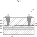
- Fig. 5 is a cross-sectional view taken along line V-V' of the zener diode 401 of the present invention.
- the Ge layer 114 is formed on an n-type silicon slab 119 and not on a p-type silicon (Si) region 111b.
- the Ge layer 114 is provided between the electrodes 117 and 118.
- the p-type silicon region 111b in the core layer 110 is not immediately below the Ge layer 114, and the n-type silicon slab 119 is under the Ge layer 114.
- the p-type silicon region 111b may be immediately below the Ge layer 114.
- the Ge layer 114 is formed by implanting a Ge material using a mask during a manufacturing step, the positional deviation from the PN junction corresponding to the p-semiconductor portion and the n-type semiconductor portion, or the p-type semiconductor portion, the i-type semiconductor portion, and the n-type semiconductor portion (pin junction) may occur, and there is a problem that the positional deviation affects the rectification characteristics of the photodetector. Meanwhile, in the detector according to the embodiment of the present invention described above with reference to Figs.
- the detector according to the embodiment of the present invention has an advantage that a problem that has occurred when the Ge layer 114 is present can be solved. Specifically, the interface between Ge and Si serves as a leakage current path, which causes variations in a reverse current when the alignment accuracy between the PN junction and the Ge layer 114 is not good. However, the detector according to the embodiment of the present invention can suppress such variations.
- the present invention relates to a photodetector used in an optical communication system or an optical information processing system, and can be particularly applied to a photodetector having resistance to electrostatic discharge.
Landscapes
- Light Receiving Elements (AREA)
Abstract
A photodetector of the present invention includes: a photodiode; and a protection diode. The photodiode and the protection diode are integrated on a same semiconductor substrate. The photodiode includes a semiconductor portion made of at least one type of semiconductor material, an anode electrode, and a cathode electrode. The protection diode includes a core layer, a semiconductor portion provided in the core layer and including a first-type semiconductor region doped with first-type impurity ions and a second-type semiconductor region doped with second-type impurity ions, an anode electrode, and a cathode electrode. The semiconductor portion of the protection diode includes only one type of semiconductor material used for the semiconductor portion of the photodiode. The anode electrodes of the protection diode and the photodiode are connected to each other. The cathode electrodes of the protection diode and the photodiode are connected to each other.
Description
- The present invention relates to a photodetector used in an optical communication system or an optical information processing system, and particularly relates to a structure for providing a photodetector having resistance to electrostatic discharge.
- With the recent spread of optical communication, cost reduction of an optical communication apparatus is required. As one of the solutions is a method of forming an optical circuit constituting the optical communication apparatus on a large-diameter wafer such as a silicon wafer using a minute optical circuit technology such as silicon photonics. As a result, a material cost per chip can be reduced, and the cost of the optical communication apparatus can be reduced.
- A representative photodetector formed on a silicon (Si) substrate using such a technology includes a germanium photodetector (hereinafter, also referred to as GePD) allowing monolithic integration (Patent Literature 1). However, this photodetector does not include a protection circuit, and therefore has a problem of being susceptible to electrostatic discharge.
- Meanwhile, Patent Literature 2 discloses a photodetector including a protection circuit (protection zener diode). The protection zener diode of the photodetector is formed using both a Ge layer and a Si layer.
-
- Patent Literature 1:
JP 5370857 B - Patent Literature 2:
JP 6981365 B - However, the photodetector including the protection zener diode of Patent literature 2 performs ion implantation (doping step) using a mask in order to form each of the Ge layer and the Si layer. At that time, due to a manufacturing error, the zener diode for the protection circuit may cause a positional deviation between a light-absorbing layer (Ge layer) and a p-type semiconductor portion, an n-type semiconductor portion (pn junction), or a p-type semiconductor portion, an intrinsic semiconductor portion, and an n-type semiconductor portion (pin junction) on a Si core layer. There is a problem that this positional deviation affects the rectification characteristics of the photodetector.
- The present invention has been made in view of such a problem, and an object of the present invention is to provide a photodetector capable of eliminating an influence on rectification characteristics due to a positional deviation in a protection zener diode.
- In order to achieve the above object, a first aspect of the present invention is a photodetector including: a photodiode; and a protection diode. The photodiode and the protection diode are integrated on a same semiconductor substrate. The photodiode includes a semiconductor portion made of at least one type of semiconductor material, an anode electrode, and a cathode electrode. The protection diode includes a core layer, a semiconductor portion provided in the core layer and including a first-type semiconductor region doped with first-type impurity ions and a second-type semiconductor region doped with second-type impurity ions, an anode electrode, and a cathode electrode. The semiconductor portion of the protection diode includes only one type of semiconductor material used for the semiconductor portion of the photodiode. The anode electrode of the protection diode and the anode electrode of the photodiode are connected to each other. The cathode electrode of the protection diode and the cathode electrode of the photodiode are connected to each other.
- The photodetector of the present invention can eliminate the influence on the rectification characteristics due to the positional deviation in the protection zener diode.
-
-
Fig. 1 is a view illustrating a top view according to a first embodiment of the present invention. -
Fig. 2 is a view illustrating the cross-sectional structure of a zener diode included in a photodetector according to the first embodiment of the present invention. -
Fig. 3 is a view illustrating the upper surface of a photodetector according to a second embodiment of the present invention. -
Fig. 4 is a view illustrating a top view of a photodetector of Comparative Example. -
Fig. 5 is a view illustrating the cross-sectional structure of a zener diode included in the photodetector of Comparative Example. - Hereinafter, a form of a photodetector of the present invention will be described in detail with reference to embodiments and drawings. In the drawings, portions having the same functions are denoted by the same numbers to clarify the description. However, the present invention is not limited to contents described in the embodiments described below, and it is obvious to those skilled in the art that the forms and the details can be variously changed without departing from the spirit of the invention disclosed in the present specification and the like.
-
Fig. 1 is a top view illustrating the configuration of a photodetector according to an embodiment of the present invention. - The photodetector according to the embodiment of the present invention is configured by electrically connecting a
GePD 300 and aprotection zener diode 301 in parallel. - The GePD 300 includes a
core layer 110 doped with a first-type impurity (n-type impurity), a (optical)waveguide 109 connected to thecore layer 110, a light-absorbing layer (Ge layer) 114 doped with a second-type impurity on thecore layer 110, a lower cladding layer 102 (seeFig. 2 ) below thecore layer 110, a semiconductor substrate 101 (seeFig. 2 ) below thelower cladding layer 102, and an upper cladding layer 103 (seeFig. 2 ) above thecore layer 110 and the light-absorbing layer. In thecore layer 110, a p-type silicon slab 111a and p++silicon contact regions type Ge region 115 is formed in the light-absorbinglayer 114. The p++silicon contact regions type Ge region 115 are provided withelectrodes core layer 110 and is absorbed by the light-absorbinglayer 114, a current flows between theelectrode 117 and theelectrodes - In the present embodiment, the GePD 300 and the
zener diode 301 are linearly arranged when viewed from thewaveguide 109, and are arranged in the incident direction of light from thewaveguide 109. - In the
zener diode 301, a p-type silicon slab (region) 111b doped with p-type impurity ions, a p++silicon contact region 112 doped with a p-type impurity at a high concentration and playing a role of forming ohmic contact with theelectrode 116, an n-type silicon slab 119 doped with n-type impurity ions, and an n++silicon contact region 120 doped with an n-type impurity at a high concentration and playing a role of forming ohmic contact with theelectrode 117 are formed in thecore layer 110 continuous with theGePD 300. The n-type silicon slab 119 is also referred to as an n-type Si slab or an n-type silicon region. The n++ silicon contact region is also referred to as an n-part silicon contact region or an n-type electrode part. On the p++silicon contact region 112 and the n++silicon contact region 120, an upper cladding layer 103 (seeFig. 2 ) similarly continuous with theGePD 300 is formed, and theelectrode 116 and theelectrode 117 are formed so as to be in contact with the p++silicon contact region 112 and the n++silicon contact region 120, respectively, via a plurality of openings formed in theupper cladding layer 103. Theelectrodes electrodes GePD 300. -
Fig. 2 is a cross-sectional view of thezener diode 301 taken along line II-II'. In thecore layer 110, the p++silicon contact region 112 is located on the p-type silicon region 111b and the n++silicon contact region 120 is located on the n-type silicon slab 119. The p++silicon contact region 112 is connected to theelectrode 116, and the n++silicon contact region 120 is connected to theelectrode 117. Anintrinsic silicon region 125 without ion implantation is present between the p-type silicon region 111b and the n-type silicon slab 119. InFig. 2 , the operation threshold value of the zener diode is determined by the size of theintrinsic silicon region 125 indicated by an arrow and the doping concentrations of the p-type silicon region 111b and the n-type silicon slab 119. In order to adjust the operation threshold value, theintrinsic silicon region 125 may be eliminated, and the p-type silicon region 111b and the n-type silicon slab 119 may be brought into contact with each other to form a PN junction. - The
upper cladding layer 103 is directly formed on the p-type semiconductor portion (the p-type silicon region 111b and the p++ silicon contact region 112), the I-type semiconductor portion (the intrinsic silicon region 125), and the p-type semiconductor portion (the n-type silicon slab 119 and the n++ silicon contact region 120). As will be described later in comparison with Comparative Example illustrated inFigs. 4 and5 , a Ge layer in contact with thecore layer 110 is not formed. That is, in the photodetector according to the present embodiment, theupper cladding layer 103 is directly formed on the p-type semiconductor portion and the n-type semiconductor portion, and only the upper cladding layer is provided between the electrodes connected to the p-type semiconductor portion and the n-type semiconductor portion. A semiconductor portion of a protection diode includes only one type of semiconductor material used for a semiconductor portion of the photodiode. As a result, there is no room for occurrence of a positional displacement between a pn junction including the p-type semiconductor portion and the n-type semiconductor portion and the light-absorbing layer (Ge layer), and as a result, it is possible to eliminate the influence on the rectification characteristics of the photodiode. - The applicant estimates that the reason why the photodetector of the present embodiment can be driven is as follows: an impurity doping concentration is set such that the voltage of the zener breakdown of the protection diode is smaller than the avalanche breakdown of the photodetector main body.
- The anode electrode of the
zener diode 301 is connected to the anode electrode of theGePD 300, and the cathode electrode of thezener diode 301 is connected to the cathode electrode of theGePD 300. - When the
electrode 116 functions as the anode electrode, theelectrodes electrode 116 functions as the cathode electrode, theelectrodes upper cladding layer 103 is present between theelectrodes - The
core layer 110 of theGePD 300 and the semiconductor portion (n-type silicon slab 119 and n++ silicon contact region 120) of theprotection diode 301 are made of the same material. - As described above, the
core layer 110 of theGePD 300 is the same layer as the semiconductor portion (n-type silicon slab 119 and n++ silicon contact region 120) of theprotection diode 301. - In the present embodiment, Ge is used as the main material of the light-absorbing
layer 114, but other semiconductor materials such as GeSn, InGaAs, and InGaAsP may be used. - In
Fig. 2 , theGePD 300 and theprotection diode 301 are on thecontinuous core layer 110, but not necessary, and may be fabricated on separate Si slabs. The height and material of the layer used as the Si slab are substantially the same as those of thecore layer 110, but may be separated from each other. - In the present embodiment, Si is used as the main material of the
core layer 110, but other semiconductor materials such as InP and SiC may be used. The position of the p-type semiconductor portion and the position of the n-type semiconductor portion may be reversed. As described above, theprotection diode 301 may employ a pin junction or a pn junction. Furthermore, as described above, asingle protection diode 301 may be used, or a plurality ofprotection diodes 301 may be loaded in parallel. - As illustrated in
Fig. 3 , a photodetector according to an embodiment of the present invention is configured by electrically connecting aGePD 300 and azener diode 301 as a protection circuit in series. - The
GePD 300 has a configuration in which theGePD 300 and thezener diode 301 are linearly arranged when viewed from thewaveguide 109 in the first embodiment ofFig. 1 , but has a configuration in which theGePD 300 and theZener diode 301 are not linearly arranged when viewed from thewaveguide 109 and are arranged in a direction orthogonal to the incident direction of light from thewaveguide 109 in a second embodiment ofFig. 3 . The longitudinal direction of theGe layer 114 of theGePD 300 and the longitudinal direction of the p++silicon contact region 112 and the n++silicon contact region 120 of thezener diode 301 are in a substantially parallel relationship. A sectional view taken along dashed line II-II' inFig. 3 corresponds toFig. 2 . - In the configuration of
Fig. 3 , the light traveling straight from thewaveguide 109 does not enter thezener diode 301, and therefore the zener diode does not detect a photocurrent. - Also in the present embodiment, a semiconductor portion of the
protection diode 301 is made of only one of semiconductor materials used for a semiconductor portion of thephotodiode 300. Therefore, it is possible to provide a photodetector including a protection circuit in which the rectification characteristics of the photodetector of the present embodiment is not affected by a positional deviation between a light-absorbing layer (Ge layer) and a pn junction including a p-type semiconductor portion and an n-type semiconductor portion, or a p-type semiconductor portion, an I-type semiconductor portion, an n-type semiconductor portion (pin junction). - Although one zener diode (protection diode) 301 is connected to the
GePD 300 inFig. 3 , a plurality ofzener diodes 301 may be connected. In that case, although the high-speed operation characteristics of the GePD are affected, high resistance to electrostatic discharge can be obtained. -
Figs. 4 and5 illustrate the configuration of a photodetector of Comparative Example. AGePD 300 has the same configuration as that of theGePD 300 of the first and second embodiments. In Comparative Example, theGePD 300 and azener diode 401 are linearly arranged when viewed from awaveguide 109, and are arranged in the incident direction of light from thewaveguide 109. A sectional view taken along line V-V' inFig. 4 corresponds toFig. 5 . - The
zener diode 401 of the present Comparative Example is different from thezener diode 301 of the first and second embodiments in that aGe layer 114 is present in a zener diode for a protection circuit. A positional deviation may occur between the Ge layer and a p-type semiconductor portion, an n-type semiconductor portion (pn junction), or a p-type semiconductor portion, an intrinsic semiconductor portion, and an n-type semiconductor portion (pin junction) on a Si core layer, and there is a problem that the positional deviation affects the rectification characteristics of the photodetector. -
Fig. 5 is a cross-sectional view taken along line V-V' of thezener diode 401 of the present invention. TheGe layer 114 is formed on an n-type silicon slab 119 and not on a p-type silicon (Si)region 111b. TheGe layer 114 is provided between theelectrodes - The p-
type silicon region 111b in thecore layer 110 is not immediately below theGe layer 114, and the n-type silicon slab 119 is under theGe layer 114. The p-type silicon region 111b may be immediately below theGe layer 114. - Since the
Ge layer 114 is formed by implanting a Ge material using a mask during a manufacturing step, the positional deviation from the PN junction corresponding to the p-semiconductor portion and the n-type semiconductor portion, or the p-type semiconductor portion, the i-type semiconductor portion, and the n-type semiconductor portion (pin junction) may occur, and there is a problem that the positional deviation affects the rectification characteristics of the photodetector. Meanwhile, in the detector according to the embodiment of the present invention described above with reference toFigs. 1 to 3 , no Ge layer is present under theupper cladding layer 103, and therefore there is no room for occurrence of the positional deviation, which makes it possible to eliminate the influence on the rectification characteristics of the photodetector. The detector according to the embodiment of the present invention has an advantage that a problem that has occurred when theGe layer 114 is present can be solved. Specifically, the interface between Ge and Si serves as a leakage current path, which causes variations in a reverse current when the alignment accuracy between the PN junction and theGe layer 114 is not good. However, the detector according to the embodiment of the present invention can suppress such variations. - The present invention relates to a photodetector used in an optical communication system or an optical information processing system, and can be particularly applied to a photodetector having resistance to electrostatic discharge.
-
- 101
- semiconductor substrate
- 102
- lower cladding layer
- 103
- upper cladding layer
- 109
- waveguide
- 110
- core layer
- 111a
- p-type silicon slab
- 111b
- p-type silicon slab (region)
- 112
- silicon contact region
- 113
- p++ silicon contact region
- 114
- light-absorbing layer (Ge layer)
- 115
- n-type Ge region
- 116
- electrode
- 117
- electrode
- 118
- electrode
- 119
- n-type silicon slab
- 120
- silicon contact region
- 125
- intrinsic silicon region
- 300
- GePD
- 301
- protection (zener) diode
- 401
- protection (zener) diode
Claims (9)
- A photodetector comprising:a photodiode; anda protection diode,wherein:the photodiode and the protection diode are integrated on a same semiconductor substrate;the photodiode includes a semiconductor portion made of at least one type of semiconductor material, an anode electrode, and a cathode electrode;the protection diode includes a core layer, a semiconductor portion provided in the core layer and including a first-type semiconductor region doped with first-type impurity ions and a second-type semiconductor region doped with second-type impurity ions, an anode electrode, and a cathode electrode;the semiconductor portion of the protection diode includes only one type of semiconductor material used for the semiconductor portion of the photodiode;the anode electrode of the protection diode and the anode electrode of the photodiode are connected to each other; andthe cathode electrode of the protection diode and the cathode electrode of the photodiode are connected to each other.
- The photodetector according to claim 1, wherein
the semiconductor portion of the photodiode includes:a core layer doped with a first-type impurity;an optical waveguide connected to the core layer;a light-absorbing layer doped with a second-type impurity on the core layer;a lower cladding layer below the core layer;an upper cladding layer on the core layer and the light-absorbing layer; andan electrode connected to each of the core layer and the light-absorbing layer. - The photodetector according to claim 2, wherein the core layer of the photodiode and the semiconductor portion of the protection diode are made of the same material.
- The photodetector according to claim 2 or 3, wherein the core layer of the photodiode and the semiconductor portion of the protection diode share the same layer.
- The photodetector according to claim 2, wherein a main material of the core layer of the photodiode is silicon, and a main material of the light-absorbing layer is germanium.
- The photodetector according to claim 1 or 2, wherein the photodiode and the protection diode are arranged in an incident direction of light passing through a silicon waveguide layer included in the photodiode.
- The photodetector according to claim 1 or 2, wherein the photodiode and the protection diode are arranged in a direction perpendicular to an incident direction of light passing through a silicon waveguide layer included in the photodiode.
- The photodetector according to claim 1 or 2, wherein a plurality of the protection diodes are connected to the photodiode.
- The photodetector according to claim 1 or 2, wherein only the upper cladding layer is formed on the semiconductor portion of the protection diode and between the electrodes of the protection diode.
Applications Claiming Priority (1)
| Application Number | Priority Date | Filing Date | Title |
|---|---|---|---|
| PCT/JP2022/026391 WO2024004175A1 (en) | 2022-06-30 | 2022-06-30 | Photodetector |
Publications (1)
| Publication Number | Publication Date |
|---|---|
| EP4550427A1 true EP4550427A1 (en) | 2025-05-07 |
Family
ID=89382554
Family Applications (1)
| Application Number | Title | Priority Date | Filing Date |
|---|---|---|---|
| EP22949448.9A Pending EP4550427A1 (en) | 2022-06-30 | 2022-06-30 | Photodetector |
Country Status (5)
| Country | Link |
|---|---|
| US (1) | US20250386601A1 (en) |
| EP (1) | EP4550427A1 (en) |
| JP (1) | JP7846415B2 (en) |
| CN (1) | CN119452758A (en) |
| WO (1) | WO2024004175A1 (en) |
Family Cites Families (5)
| Publication number | Priority date | Publication date | Assignee | Title |
|---|---|---|---|---|
| JP5370857B2 (en) | 2010-03-04 | 2013-12-18 | 日本電信電話株式会社 | GERMANIUM RECEIVER AND MANUFACTURING METHOD THEREOF |
| US9806112B1 (en) * | 2016-05-02 | 2017-10-31 | Huawei Technologies Co., Ltd. | Electrostatic discharge guard structure |
| US9726841B1 (en) * | 2016-07-12 | 2017-08-08 | Inphi Corporation | Integrated photo detector, method of making the same |
| US10578800B2 (en) * | 2017-06-06 | 2020-03-03 | Sifotonics Technologies Co., Ltd. | Silicon photonic integrated circuit with electrostatic discharge protection mechanism for static electric shocks |
| JP6981365B2 (en) * | 2018-05-17 | 2021-12-15 | 日本電信電話株式会社 | Photodetector |
-
2022
- 2022-06-30 JP JP2024530234A patent/JP7846415B2/en active Active
- 2022-06-30 EP EP22949448.9A patent/EP4550427A1/en active Pending
- 2022-06-30 US US18/878,177 patent/US20250386601A1/en active Pending
- 2022-06-30 CN CN202280097486.8A patent/CN119452758A/en active Pending
- 2022-06-30 WO PCT/JP2022/026391 patent/WO2024004175A1/en not_active Ceased
Also Published As
| Publication number | Publication date |
|---|---|
| CN119452758A (en) | 2025-02-14 |
| US20250386601A1 (en) | 2025-12-18 |
| JPWO2024004175A1 (en) | 2024-01-04 |
| JP7846415B2 (en) | 2026-04-15 |
| WO2024004175A1 (en) | 2024-01-04 |
Similar Documents
| Publication | Publication Date | Title |
|---|---|---|
| US4992386A (en) | Method of manufacturing a semiconductor light detector | |
| JP3601761B2 (en) | Light receiving element and method of manufacturing the same | |
| EP1811578B1 (en) | Avalanche photodiode | |
| US8871557B2 (en) | Photomultiplier and manufacturing method thereof | |
| EP0473197A1 (en) | Photo-sensing device | |
| US5880489A (en) | Semiconductor photodetector | |
| US20230083263A1 (en) | Light detector, light detection system, lidar device, and mobile body | |
| KR19980058393A (en) | Avalanche Photodiode and Manufacturing Method Thereof | |
| EP2669934B1 (en) | Semiconductor device | |
| EP3988908B1 (en) | Photodetector and method for manufacturing photodetector | |
| US12142616B2 (en) | Light detector, light detection system, LIDAR device, and mobile body | |
| CN112119507B (en) | Light detector | |
| US20220013550A1 (en) | Photodetector | |
| US6831308B2 (en) | Semiconductor light detecting device | |
| US20250386601A1 (en) | Photodetector | |
| KR970005150B1 (en) | Phto detector and opto-electronic intergrated circuit | |
| JPH0513798A (en) | Semiconductor light receiving device | |
| US12224368B1 (en) | Optoelectronic device including photodiode having buried layer with different thicknesses | |
| US20250287721A1 (en) | Semiconductor light-receiving element | |
| JP7663522B2 (en) | Optical detector, optical detection system, lidar device, and moving object | |
| US20240234593A1 (en) | Light-receiving element and light detection device | |
| EP3576150A1 (en) | Image-capture element and method for manufacturing image-capture element | |
| JP2763352B2 (en) | Semiconductor light receiving element | |
| JP2025162851A (en) | Light receiving element and its manufacturing method | |
| JP2024076062A (en) | Light receiving element and light detection device |
Legal Events
| Date | Code | Title | Description |
|---|---|---|---|
| STAA | Information on the status of an ep patent application or granted ep patent |
Free format text: STATUS: THE INTERNATIONAL PUBLICATION HAS BEEN MADE |
|
| PUAI | Public reference made under article 153(3) epc to a published international application that has entered the european phase |
Free format text: ORIGINAL CODE: 0009012 |
|
| STAA | Information on the status of an ep patent application or granted ep patent |
Free format text: STATUS: REQUEST FOR EXAMINATION WAS MADE |
|
| 17P | Request for examination filed |
Effective date: 20241227 |
|
| AK | Designated contracting states |
Kind code of ref document: A1 Designated state(s): AL AT BE BG CH CY CZ DE DK EE ES FI FR GB GR HR HU IE IS IT LI LT LU LV MC MK MT NL NO PL PT RO RS SE SI SK SM TR |
|
| RAP3 | Party data changed (applicant data changed or rights of an application transferred) |
Owner name: NTT, INC. |
|
| DAV | Request for validation of the european patent (deleted) | ||
| DAX | Request for extension of the european patent (deleted) |