EP4550391A1 - Method for fabricating semiconductor packaging structure and semiconductor packaging structure fabricated using the same - Google Patents
Method for fabricating semiconductor packaging structure and semiconductor packaging structure fabricated using the same Download PDFInfo
- Publication number
- EP4550391A1 EP4550391A1 EP24172388.1A EP24172388A EP4550391A1 EP 4550391 A1 EP4550391 A1 EP 4550391A1 EP 24172388 A EP24172388 A EP 24172388A EP 4550391 A1 EP4550391 A1 EP 4550391A1
- Authority
- EP
- European Patent Office
- Prior art keywords
- semiconductor
- lower mold
- packaging structure
- metal structures
- sidewall
- Prior art date
- Legal status (The legal status is an assumption and is not a legal conclusion. Google has not performed a legal analysis and makes no representation as to the accuracy of the status listed.)
- Pending
Links
Images





Classifications
-
- H—ELECTRICITY
- H10—SEMICONDUCTOR DEVICES; ELECTRIC SOLID-STATE DEVICES NOT OTHERWISE PROVIDED FOR
- H10W—GENERIC PACKAGES, INTERCONNECTIONS, CONNECTORS OR OTHER CONSTRUCTIONAL DETAILS OF DEVICES COVERED BY CLASS H10
- H10W72/00—Interconnections or connectors in packages
- H10W72/01—Manufacture or treatment
- H10W72/0198—Manufacture or treatment batch processes
-
- H—ELECTRICITY
- H10—SEMICONDUCTOR DEVICES; ELECTRIC SOLID-STATE DEVICES NOT OTHERWISE PROVIDED FOR
- H10W—GENERIC PACKAGES, INTERCONNECTIONS, CONNECTORS OR OTHER CONSTRUCTIONAL DETAILS OF DEVICES COVERED BY CLASS H10
- H10W74/00—Encapsulations, e.g. protective coatings
- H10W74/01—Manufacture or treatment
- H10W74/014—Manufacture or treatment using batch processing
-
- H—ELECTRICITY
- H10—SEMICONDUCTOR DEVICES; ELECTRIC SOLID-STATE DEVICES NOT OTHERWISE PROVIDED FOR
- H10W—GENERIC PACKAGES, INTERCONNECTIONS, CONNECTORS OR OTHER CONSTRUCTIONAL DETAILS OF DEVICES COVERED BY CLASS H10
- H10W74/00—Encapsulations, e.g. protective coatings
- H10W74/01—Manufacture or treatment
- H10W74/016—Manufacture or treatment using moulds
-
- H—ELECTRICITY
- H10—SEMICONDUCTOR DEVICES; ELECTRIC SOLID-STATE DEVICES NOT OTHERWISE PROVIDED FOR
- H10W—GENERIC PACKAGES, INTERCONNECTIONS, CONNECTORS OR OTHER CONSTRUCTIONAL DETAILS OF DEVICES COVERED BY CLASS H10
- H10W74/00—Encapsulations, e.g. protective coatings
- H10W74/01—Manufacture or treatment
- H10W74/019—Manufacture or treatment using temporary auxiliary substrates
-
- H—ELECTRICITY
- H10—SEMICONDUCTOR DEVICES; ELECTRIC SOLID-STATE DEVICES NOT OTHERWISE PROVIDED FOR
- H10W—GENERIC PACKAGES, INTERCONNECTIONS, CONNECTORS OR OTHER CONSTRUCTIONAL DETAILS OF DEVICES COVERED BY CLASS H10
- H10W74/00—Encapsulations, e.g. protective coatings
- H10W74/10—Encapsulations, e.g. protective coatings characterised by their shape or disposition
- H10W74/111—Encapsulations, e.g. protective coatings characterised by their shape or disposition the semiconductor body being completely enclosed
-
- H—ELECTRICITY
- H10—SEMICONDUCTOR DEVICES; ELECTRIC SOLID-STATE DEVICES NOT OTHERWISE PROVIDED FOR
- H10W—GENERIC PACKAGES, INTERCONNECTIONS, CONNECTORS OR OTHER CONSTRUCTIONAL DETAILS OF DEVICES COVERED BY CLASS H10
- H10W74/00—Encapsulations, e.g. protective coatings
- H10W74/10—Encapsulations, e.g. protective coatings characterised by their shape or disposition
- H10W74/111—Encapsulations, e.g. protective coatings characterised by their shape or disposition the semiconductor body being completely enclosed
- H10W74/114—Encapsulations, e.g. protective coatings characterised by their shape or disposition the semiconductor body being completely enclosed by a substrate and the encapsulations
-
- H—ELECTRICITY
- H10—SEMICONDUCTOR DEVICES; ELECTRIC SOLID-STATE DEVICES NOT OTHERWISE PROVIDED FOR
- H10W—GENERIC PACKAGES, INTERCONNECTIONS, CONNECTORS OR OTHER CONSTRUCTIONAL DETAILS OF DEVICES COVERED BY CLASS H10
- H10W74/00—Encapsulations, e.g. protective coatings
-
- H—ELECTRICITY
- H10—SEMICONDUCTOR DEVICES; ELECTRIC SOLID-STATE DEVICES NOT OTHERWISE PROVIDED FOR
- H10W—GENERIC PACKAGES, INTERCONNECTIONS, CONNECTORS OR OTHER CONSTRUCTIONAL DETAILS OF DEVICES COVERED BY CLASS H10
- H10W74/00—Encapsulations, e.g. protective coatings
- H10W74/10—Encapsulations, e.g. protective coatings characterised by their shape or disposition
- H10W74/131—Encapsulations, e.g. protective coatings characterised by their shape or disposition the semiconductor body being only partially enclosed
- H10W74/137—Encapsulations, e.g. protective coatings characterised by their shape or disposition the semiconductor body being only partially enclosed the encapsulations being directly on the semiconductor body
Definitions
- the present invention relates to a method for fabricating a semiconductor packaging structure, and, in particular, to a method for fabricating a semiconductor packaging structure by disposing posts.
- a method for fabricating a semiconductor packaging structure includes providing a lower mold.
- the fabrication method includes disposing a plurality of semiconductor components on the lower mold.
- the fabrication method includes disposing a plurality of first metal structures on the lower mold, wherein the first metal structures are located on both sides of the semiconductor components.
- the fabrication method includes providing an upper mold to assemble with the lower mold to accommodate the semiconductor components and the first metal structures.
- the fabrication method includes filling a packaging material between the lower mold and the upper mold.
- the fabrication method includes removing the upper mold, the lower mold and the first metal structures to form a plurality of through holes in the packaging material located on both sides of the semiconductor components.
- the step of disposing the semiconductor components and the first metal structures on the lower mold includes providing a carrier; disposing a tape on the carrier; disposing the semiconductor components and the first metal structures on the tape; and disposing the carrier on the lower mold.
- the step of disposing the semiconductor components on the lower mold includes providing a carrier; disposing the semiconductor components on the carrier; and transferring the semiconductor components to the lower mold.
- the method for fabricating a semiconductor packaging structure further includes transferring the semiconductor components to the lower mold through a plurality of second metal structures disposed on the lower mold.
- the step of disposing the first metal structures on the lower mold includes locking the first metal structures to the upper mold; and assembling the upper mold and the lower mold.
- the method for fabricating a semiconductor packaging structure further includes cutting the packaging material to form a plurality of semiconductor packaging structures, wherein each semiconductor packaging structure includes a semiconductor component, a packaging material covering the semiconductor component, and through holes penetrating the packaging material.
- the packaging material in each of the semiconductor packaging structures, has a first sidewall and a second sidewall opposite the first sidewall, and the angle between the first sidewall and the second sidewall and the horizontal plane is 90 degrees.
- a semiconductor packaging structure which is fabricated by the disclosed method for fabricating a semiconductor packaging structure is provided.
- the packaging material has a first sidewall and a second sidewall opposite the first sidewall, and the angle between the first sidewall and the second sidewall and the horizontal plane is 90 degrees.
- the semiconductor packaging structure further includes a plurality of positioning holes located on both sides of the semiconductor component, wherein the positioning holes are closer to the semiconductor component than the through holes.
- the present disclosure utilizes cutting and molding technology after demolding to easily produce products with vertical sides, overcoming traditional manufacturing process limitations.
- first component when referred to as "on a second component", it may directly contact the second component, or there may be other components in between, and the first component and the second component do not come in direct contact with one another.
- spatial terms may be used, such as “below”, “lower”, “above”, “higher” and similar terms, for briefly describing the relationship between an element relative to another element in the figures.
- the components may be used or operated in different directions.
- the spatially related adjectives used in it will also be interpreted according to the turned position.
- terms concerning attachments, coupling and the like, such as “connected” and “interconnected,” refer to a relationship wherein structures are secured or attached to one another either directly or indirectly through intervening structures, as well as both movable or rigid attachments or relationships, unless expressly described otherwise.
- the terms “about”, “around” and “substantially” typically mean a value is in a range of +/- 15% of a stated value, typically a range of +/- 10% of the stated value, typically a range of +/- 5% of the stated value, typically a range of +/- 3% of the stated value, typically a range of +/- 2% of the stated value, typically a range of +/- 1% of the stated value, or typically a range of +/- 0.5% of the stated value.
- the stated value of the present disclosure is an approximate value. Namely, the meaning of "about”, “around” and “substantially” may be implied if there is no specific description of "about”, “around” and “substantially”.
- first, second, third, etc. may be used herein to describe various elements, components, regions, layers, portions and/or sections, these elements, components, regions, layers, portions and/or sections should not be limited by these terms. These terms are only used to distinguish one element, component, region, layer, portion or section from another element, component, region, layer, portion or section. Thus, a first element, component, region, layer, portion or section discussed below could be termed a second element, component, region, layer, portion or section without departing from the teachings of the present disclosure.
- FIG. 1 shows a cross-sectional view of the mold-cladding semiconductor structure 10.
- the mold-cladding semiconductor structure 10 includes a lower mold 12, a carrier 14, a tape 16, a plurality of semiconductor components 18, a plurality of first metal structures 20, a packaging material 22, and an upper mold 24.
- the semiconductor components 18 are disposed on the lower mold 12.
- the carrier 14 is disposed between the lower mold 12 and the semiconductor components 18.
- the tape 16 is disposed between the carrier 14 and the semiconductor components 18.
- the first metal structures 20 are disposed on the lower mold 12 and located on both sides of the semiconductor components 18. In more detail, the semiconductor components 18 and the first metal structures 20 are disposed on the tape 16 and in contact with the tape 16.
- the packaging material 22 is filled between the lower mold 12 and the upper mold 24.
- the first metal structures 20 penetrate the packaging material 22.
- the upper mold 24 is assembled with the lower mold 12 to accommodate the semiconductor components 18 and the first metal structures 20.
- the carrier 14 may include metal, but the present disclosure is not limited thereto, and other suitable hard materials with heat-resistant, pressure-resistant and support properties are also applicable to the present disclosure.
- the tape 16 may include heat-resistant tape, but the present disclosure is not limited thereto, and other suitable materials with heat-resistant, pressure-resistant and adhesive properties are also applicable to the present disclosure.
- the semiconductor components 18 may include power components, but the present disclosure is not limited thereto.
- the semiconductor component 18 may include a substrate 26, a first metal layer 28, a second metal layer 30, a conductive component 32, and a chip 33.
- the first metal layer 28 and the second metal layer 30 are disposed on opposite sides of the substrate 26.
- the first metal layer 28 is in contact with the tape 16.
- the conductive component 32 is disposed on the second metal layer 30 to connect to an external circuit (not shown).
- the chip 33 is disposed on the second metal layer 30, as shown in FIG. 1 .
- the first metal structures 20 may include columnar metal structures, for example, cylindrical metal structures, but the present disclosure is not limited thereto, and other suitable three-dimensional shapes are also applicable to the present disclosure, and may be designed according to product requirements.
- a plurality of first metal structures 20 may be included. For example, between the adjacent semiconductor components 18, there is an even number of the first metal structures 20, so that a semiconductor packaging structure formed after cutting has symmetrical through holes for subsequent screw locking, but the present disclosure is not limited thereto, and other suitable locations and quantities of the first metal structures 20 are also applicable to the present disclosure, and may be designed according to product requirements.
- the packaging material 22 may include solid molding materials, liquid molding materials, anisotropic conductive film (ACF), or sheet molding materials, but the present disclosure is not limited thereto, and other suitable molding materials are also applicable to the present disclosure.
- ACF anisotropic conductive film
- FIG. 2 shows a cross-sectional view of the mold-cladding semiconductor structure 100.
- the mold-cladding semiconductor structure 100 includes a lower mold 120, a plurality of semiconductor components 180, a plurality of first metal structures 200, a plurality of second metal structures 210, a packaging material 220, and an upper mold 240.
- the semiconductor components 180 are disposed on the lower mold 120.
- the first metal structures 200 are disposed on the lower mold 120 and located on both sides of the semiconductor components 180.
- the second metal structures 210 are disposed on the lower mold 120 and located on both sides of the semiconductor components 180.
- the semiconductor components 180, the first metal structures 200 and the second metal structures 210 are disposed on the lower mold 120 and in contact with the lower mold 120.
- the second metal structures 210 are closer to the semiconductor component 180 than the first metal structures 200.
- the packaging material 220 is filled between the lower mold 120 and the upper mold 240.
- the first metal structures 200 penetrate the packaging material 220.
- the upper mold 240 is assembled with the lower mold 120 to accommodate the semiconductor components 180, the first metal structures 200 and the second metal structures 210.
- the semiconductor components 180 may include power components, but the present disclosure is not limited thereto.
- the semiconductor component 180 may include a substrate 260, a first metal layer 280, a second metal layer 300, a conductive component 320, and a chip 330.
- the first metal layer 280 and the second metal layer 300 are disposed on opposite sides of the substrate 260.
- the first metal layer 280 is in contact with the lower mold 120.
- the conductive component 320 is disposed on the second metal layer 300 to connect to an external circuit (not shown).
- the chip 330 is disposed on the second metal layer 300, as shown in FIG. 2 .
- the first metal structures 200 may include columnar metal structures, for example, cylindrical metal structures, but the present disclosure is not limited thereto, and other suitable three-dimensional shapes are also applicable to the present disclosure, and may be designed according to product requirements.
- a plurality of first metal structures 200 may be included between the adjacent semiconductor components 180. For example, between the adjacent semiconductor components 180, there is an even number of the first metal structures 200, so that a semiconductor packaging structure formed after cutting has symmetrical through holes for subsequent screw locking, but the present disclosure is not limited thereto, and other suitable locations and quantities of the first metal structures 200 are also applicable to the present disclosure, and may be designed according to product requirements.
- the second metal structures 210 may include columnar metal structures, for example, cylindrical metal structures, but the present disclosure is not limited thereto, and other suitable three-dimensional shapes are also applicable to the present disclosure, and may be designed according to product requirements.
- the second metal structure 210 is disposed at a specific position on the lower mold 120 to serve as a positioning post for transferring the semiconductor component 180 to the lower mold 120, so that the semiconductor component 180 can be smoothly disposed at a predetermined position on the lower mold 120.
- the packaging material 220 may include solid molding materials, liquid molding materials, anisotropic conductive film (ACF), or sheet molding materials, but the present disclosure is not limited thereto, and other suitable molding materials are also applicable to the present disclosure.
- ACF anisotropic conductive film
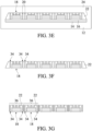
- FIGS. 3A-3H in accordance with one embodiment of the present disclosure, a method for fabricating a semiconductor packaging structure is provided.
- FIGS. 3A-3H show cross-sectional views of the method for fabricating the semiconductor packaging structure.
- a carrier 14 is provided.
- a tape 16 is attached to the carrier 14.
- the semiconductor component 18 includes a substrate 26, a first metal layer 28, a second metal layer 30, a conductive component 32, and a chip 33.
- the first metal layer 28 and the second metal layer 30 are disposed on opposite sides of the substrate 26.
- the first metal layer 28 is in contact with the tape 16.
- the conductive component 32 is disposed on the second metal layer 30 for subsequent connection to external circuits.
- the chip 33 is disposed on the second metal layer 30.
- a plurality of first metal structures 20 are attached to the tape 16 and located on both sides of the semiconductor components 18.
- the positions where the first metal structures 20 are attached to the tape 16 are the positions where the through holes are subsequently formed.
- a lower mold 12 is provided.
- the carrier 14 with the tape 16, the semiconductor components 18 and the first metal structures 20 disposed thereon is disposed on the lower mold 12. That is, the semiconductor components 18 and the first metal structures 20 are disposed on the lower mold 12.
- an upper mold 24 is provided.
- the upper mold 24 is assembled with the lower mold 12 to accommodate the semiconductor components 18 and the first metal structures 20.
- a packaging material 22 is injected and filled between the lower mold 12 and the upper mold 24.
- the upper mold 24, the lower mold 12, the first metal structures 20, the carrier 14 and the tape 16 are removed to form a plurality of through holes 34 in the packaging material 22 on both sides of the semiconductor components 18.
- the packaging material 22 is cut, for example, by laser cutting, to form a plurality of first semiconductor packaging structures 36.
- Each first semiconductor packaging structure 36 includes the semiconductor component 18, the packaging material 22 covering the semiconductor component 18, and the through holes 34 penetrating the packaging material 22.
- the packaging material 22 has a first sidewall 22a and a second sidewall 22b opposite the first sidewall 22a, and the angle between the first sidewall 22a and the second sidewall 22b and the horizontal plane P is 90 degrees.
- the first angle ⁇ 1 between the first sidewall 22a of the packaging material 22 and the horizontal plane P is 90 degrees.
- the second angle ⁇ 2 between the second sidewall 22b of the packaging material 22 and the horizontal plane P is 90 degrees. So far, the fabrication of the disclosed semiconductor packaging structure is completed.
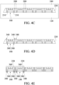
- FIGS. 4A-4F in accordance with one embodiment of the present disclosure, a method for fabricating a semiconductor packaging structure is provided.
- FIGS. 4A-4F show cross-sectional views of the method for fabricating the semiconductor packaging structure.
- a carrier 140 is provided.
- a plurality of semiconductor components 180 are disposed on the carrier 140.
- the semiconductor component 180 includes a substrate 260, a first metal layer 280, a second metal layer 300, a conductive component 320, and a chip 330.
- the first metal layer 280 and the second metal layer 300 are disposed on opposite sides of the substrate 260.
- the conductive component 320 is disposed on the second metal layer 300 for subsequent connection to external circuits.
- the chip 330 is disposed on the second metal layer 300.
- a lower mold 120 is provided, wherein a plurality of second metal structures 210 are disposed at specific positions on the lower mold 120 to serve as positioning posts for transferring the semiconductor components 180 on the carrier 140 to the lower mold 120.
- the semiconductor components 180 are transferred to the lower mold 120 through the second metal structures 210 disposed on the lower mold 120, so that the semiconductor components 180 are disposed at predetermined positions on the lower mold 120.
- an upper mold 240 is provided.
- a plurality of first metal structures 200 are locked to the upper mold 240.
- the upper mold 240 with the first metal structures 200 locked thereon is assembled with the lower mold 120 to accommodate the semiconductor components 180, the first metal structures 200, and the second metal structures 210. That is, the semiconductor components 180, the first metal structures 200, and the second metal structures 210 are disposed on the lower mold 120, wherein the first metal structures 200 and the second metal structures 210 are respectively located on both sides of the semiconductor component 180, and the second metal structures 210 are closer to the semiconductor component 180 than the first metal structures 200.
- the positions of the first metal structures 200 are the positions where the through holes are subsequently formed.
- the upper mold 240, the lower mold 120, the first metal structures 200 and the second metal structures 210 are removed to form a plurality of through holes 340 and a plurality of positioning holes 380 in the packaging material 220.
- the through holes 340 and the positioning holes 380 are respectively located on both sides of the semiconductor component 180, wherein the positioning holes 380 are closer to the semiconductor component 180 than the through holes 340.
- the packaging material 220 is cut, for example, by laser cutting, to form a plurality of second semiconductor packaging structures 360.
- Each of the second semiconductor packaging structures 360 includes a semiconductor component 180, a packaging material 220 covering the semiconductor component 180, through holes 340 penetrating the packaging material 220 and positioning holes 380 adjacent to the semiconductor component 180.
- the packaging material 220 has a first sidewall 220a and a second sidewall 220b opposite the first sidewall 220a, and the angle between the first sidewall 220a and the second sidewall 220b and the horizontal plane P is 90 degrees.
- the first angle ⁇ 1 between the first sidewall 220a of the packaging material 220 and the horizontal plane P is 90 degrees.
- the second angle ⁇ 2 between the second sidewall 220b of the packaging material 220 and the horizontal plane P is 90 degrees. So far, the fabrication of the disclosed semiconductor packaging structure is completed.
- the present disclosure utilizes cutting and molding technology after demolding to easily produce products with vertical sides, overcoming traditional manufacturing process limitations.
Landscapes
- Structures Or Materials For Encapsulating Or Coating Semiconductor Devices Or Solid State Devices (AREA)
- Encapsulation Of And Coatings For Semiconductor Or Solid State Devices (AREA)
- Engineering & Computer Science (AREA)
- Microelectronics & Electronic Packaging (AREA)
Abstract
A method for fabricating a semiconductor packaging structure is provided. The fabrication method includes providing a lower mold. The fabrication method includes disposing a plurality of semiconductor components on the lower mold. The fabrication method includes disposing a plurality of first metal structures on the lower mold, wherein the first metal structures are located on both sides of the semiconductor components. The fabrication method includes providing an upper mold to assemble with the lower mold to accommodate the semiconductor components and the first metal structures. The fabrication method includes filling a packaging material between the lower mold and the upper mold. The fabrication method includes removing the upper mold, the lower mold and the first metal structures to form a plurality of through holes in the packaging material located on both sides of the semiconductor components.
Description
- This Application claims priority of
China Patent Application No. 202311446863.7, filed on November 2, 2023 - The present invention relates to a method for fabricating a semiconductor packaging structure, and, in particular, to a method for fabricating a semiconductor packaging structure by disposing posts.
- For current power modules molded with epoxy resin, the structural features of the product are designed on the mold. However, different molds need to be designed for products with different structural characteristics. That is, the molds are not interchangeable, resulting in high mold manufacturing costs.
- Also, the production of products with complex structural features is often limited by the capabilities of the molding process.
- In accordance with one embodiment of the present disclosure, a method for fabricating a semiconductor packaging structure is provided. The fabrication method includes providing a lower mold. The fabrication method includes disposing a plurality of semiconductor components on the lower mold. The fabrication method includes disposing a plurality of first metal structures on the lower mold, wherein the first metal structures are located on both sides of the semiconductor components. The fabrication method includes providing an upper mold to assemble with the lower mold to accommodate the semiconductor components and the first metal structures. The fabrication method includes filling a packaging material between the lower mold and the upper mold. The fabrication method includes removing the upper mold, the lower mold and the first metal structures to form a plurality of through holes in the packaging material located on both sides of the semiconductor components.
- In some embodiments, the step of disposing the semiconductor components and the first metal structures on the lower mold includes providing a carrier; disposing a tape on the carrier; disposing the semiconductor components and the first metal structures on the tape; and disposing the carrier on the lower mold.
- In some embodiments, the step of disposing the semiconductor components on the lower mold includes providing a carrier; disposing the semiconductor components on the carrier; and transferring the semiconductor components to the lower mold. In some embodiments, the method for fabricating a semiconductor packaging structure further includes transferring the semiconductor components to the lower mold through a plurality of second metal structures disposed on the lower mold. In some embodiments, the step of disposing the first metal structures on the lower mold includes locking the first metal structures to the upper mold; and assembling the upper mold and the lower mold.
- In some embodiments, the method for fabricating a semiconductor packaging structure further includes cutting the packaging material to form a plurality of semiconductor packaging structures, wherein each semiconductor packaging structure includes a semiconductor component, a packaging material covering the semiconductor component, and through holes penetrating the packaging material. In some embodiments, in each of the semiconductor packaging structures, the packaging material has a first sidewall and a second sidewall opposite the first sidewall, and the angle between the first sidewall and the second sidewall and the horizontal plane is 90 degrees.
- In accordance with one embodiment of the present disclosure, a semiconductor packaging structure which is fabricated by the disclosed method for fabricating a semiconductor packaging structure is provided.
- In some embodiments, the packaging material has a first sidewall and a second sidewall opposite the first sidewall, and the angle between the first sidewall and the second sidewall and the horizontal plane is 90 degrees.
- In some embodiments, the semiconductor packaging structure further includes a plurality of positioning holes located on both sides of the semiconductor component, wherein the positioning holes are closer to the semiconductor component than the through holes.
- In the present disclosure, when products of different sizes or structural features are to be produced, there is no need to design different molds. That is, different products can share the same mold, and only through the structural design of the detachable posts and subsequent cutting procedures, the required products can be produced. Through the disclosed process technology, the commonality of molds can be increased and the cost of mold development can be saved.
- Since there is no need to design the structural features of the product on the mold, the structural strength of the mold is also improved, making the mold more tolerable. In addition, The present disclosure utilizes cutting and molding technology after demolding to easily produce products with vertical sides, overcoming traditional manufacturing process limitations.
- The disclosure can be more fully understood from the following detailed description when read with the accompanying figures. It is worth noting that in accordance with standard practice in the industry, various features are not drawn to scale. In fact, the dimensions of the various features may be arbitrarily increased or reduced for clarity of discussion.
-
FIG. 1 shows a cross-sectional view of a mold-cladding semiconductor structure in accordance with one embodiment of the present disclosure; -
FIG. 2 shows a cross-sectional view of a mold-cladding semiconductor structure in accordance with one embodiment of the present disclosure; -
FIGS. 3A-3H show cross-sectional views of a method for fabricating a semiconductor packaging structure in accordance with one embodiment of the present disclosure; and -
FIGS. 4A-4F show cross-sectional views of a method for fabricating a semiconductor packaging structure in accordance with one embodiment of the present disclosure. - Various embodiments or examples are provided in the following description to implement different features of the present disclosure. The elements and arrangement described in the following specific examples are merely provided for introducing the present disclosure and serve as examples without limiting the scope of the present disclosure. For example, when a first component is referred to as "on a second component", it may directly contact the second component, or there may be other components in between, and the first component and the second component do not come in direct contact with one another.
- It should be understood that additional operations may be provided before, during, and/or after the described method. In accordance with some embodiments, some of the stages (or steps) described below may be replaced or omitted.
- In this specification, spatial terms may be used, such as "below", "lower", "above", "higher" and similar terms, for briefly describing the relationship between an element relative to another element in the figures. Besides the directions illustrated in the figures, the components may be used or operated in different directions. When the component is turned to different directions (such as rotated 45 degrees or other directions), the spatially related adjectives used in it will also be interpreted according to the turned position. In some embodiments of the present disclosure, terms concerning attachments, coupling and the like, such as "connected" and "interconnected," refer to a relationship wherein structures are secured or attached to one another either directly or indirectly through intervening structures, as well as both movable or rigid attachments or relationships, unless expressly described otherwise.
- Herein, the terms "about", "around" and "substantially" typically mean a value is in a range of +/- 15% of a stated value, typically a range of +/- 10% of the stated value, typically a range of +/- 5% of the stated value, typically a range of +/- 3% of the stated value, typically a range of +/- 2% of the stated value, typically a range of +/- 1% of the stated value, or typically a range of +/- 0.5% of the stated value. The stated value of the present disclosure is an approximate value. Namely, the meaning of "about", "around" and "substantially" may be implied if there is no specific description of "about", "around" and "substantially".
- It should be understood that, although the terms "first", "second", "third", etc. may be used herein to describe various elements, components, regions, layers, portions and/or sections, these elements, components, regions, layers, portions and/or sections should not be limited by these terms. These terms are only used to distinguish one element, component, region, layer, portion or section from another element, component, region, layer, portion or section. Thus, a first element, component, region, layer, portion or section discussed below could be termed a second element, component, region, layer, portion or section without departing from the teachings of the present disclosure.
- Unless defined otherwise, all technical and scientific terms used herein have the same meaning as commonly understood by one of ordinary skill in the art to which this disclosure belongs. It should be appreciated that, in each case, the term, which is defined in a commonly used dictionary, should be interpreted as having a meaning that conforms to the relative skills of the present disclosure and the background or the context of the present disclosure, and should not be interpreted in an idealized or overly formal manner unless so defined.
- Referring to
FIG. 1 , in accordance with one embodiment of the present disclosure, a mold-cladding semiconductor structure 10 is provided.FIG. 1 shows a cross-sectional view of the mold-cladding semiconductor structure 10. - As shown in
FIG. 1 , the mold-cladding semiconductor structure 10 includes alower mold 12, acarrier 14, atape 16, a plurality ofsemiconductor components 18, a plurality offirst metal structures 20, apackaging material 22, and anupper mold 24. Thesemiconductor components 18 are disposed on thelower mold 12. Thecarrier 14 is disposed between thelower mold 12 and thesemiconductor components 18. Thetape 16 is disposed between thecarrier 14 and thesemiconductor components 18. Thefirst metal structures 20 are disposed on thelower mold 12 and located on both sides of thesemiconductor components 18. In more detail, thesemiconductor components 18 and thefirst metal structures 20 are disposed on thetape 16 and in contact with thetape 16. Thepackaging material 22 is filled between thelower mold 12 and theupper mold 24. Thefirst metal structures 20 penetrate thepackaging material 22. Theupper mold 24 is assembled with thelower mold 12 to accommodate thesemiconductor components 18 and thefirst metal structures 20. - In some embodiments, the
carrier 14 may include metal, but the present disclosure is not limited thereto, and other suitable hard materials with heat-resistant, pressure-resistant and support properties are also applicable to the present disclosure. In some embodiments, thetape 16 may include heat-resistant tape, but the present disclosure is not limited thereto, and other suitable materials with heat-resistant, pressure-resistant and adhesive properties are also applicable to the present disclosure. - In some embodiments, the
semiconductor components 18 may include power components, but the present disclosure is not limited thereto. In some embodiments, thesemiconductor component 18 may include asubstrate 26, afirst metal layer 28, asecond metal layer 30, aconductive component 32, and achip 33. Thefirst metal layer 28 and thesecond metal layer 30 are disposed on opposite sides of thesubstrate 26. Thefirst metal layer 28 is in contact with thetape 16. Theconductive component 32 is disposed on thesecond metal layer 30 to connect to an external circuit (not shown). Thechip 33 is disposed on thesecond metal layer 30, as shown inFIG. 1 . - In some embodiments, the
first metal structures 20 may include columnar metal structures, for example, cylindrical metal structures, but the present disclosure is not limited thereto, and other suitable three-dimensional shapes are also applicable to the present disclosure, and may be designed according to product requirements. In some embodiments, between theadjacent semiconductor components 18, a plurality offirst metal structures 20 may be included. For example, between theadjacent semiconductor components 18, there is an even number of thefirst metal structures 20, so that a semiconductor packaging structure formed after cutting has symmetrical through holes for subsequent screw locking, but the present disclosure is not limited thereto, and other suitable locations and quantities of thefirst metal structures 20 are also applicable to the present disclosure, and may be designed according to product requirements. - In some embodiments, the
packaging material 22 may include solid molding materials, liquid molding materials, anisotropic conductive film (ACF), or sheet molding materials, but the present disclosure is not limited thereto, and other suitable molding materials are also applicable to the present disclosure. - Referring to
FIG. 2 , in accordance with one embodiment of the present disclosure, a mold-cladding semiconductor structure 100 is provided.FIG. 2 shows a cross-sectional view of the mold-cladding semiconductor structure 100. - As shown in
FIG. 2 , the mold-cladding semiconductor structure 100 includes alower mold 120, a plurality ofsemiconductor components 180, a plurality offirst metal structures 200, a plurality ofsecond metal structures 210, apackaging material 220, and anupper mold 240. Thesemiconductor components 180 are disposed on thelower mold 120. Thefirst metal structures 200 are disposed on thelower mold 120 and located on both sides of thesemiconductor components 180. Thesecond metal structures 210 are disposed on thelower mold 120 and located on both sides of thesemiconductor components 180. In more detail, thesemiconductor components 180, thefirst metal structures 200 and thesecond metal structures 210 are disposed on thelower mold 120 and in contact with thelower mold 120. Thesecond metal structures 210 are closer to thesemiconductor component 180 than thefirst metal structures 200. Thepackaging material 220 is filled between thelower mold 120 and theupper mold 240. Thefirst metal structures 200 penetrate thepackaging material 220. Theupper mold 240 is assembled with thelower mold 120 to accommodate thesemiconductor components 180, thefirst metal structures 200 and thesecond metal structures 210. - In some embodiments, the
semiconductor components 180 may include power components, but the present disclosure is not limited thereto. In some embodiments, thesemiconductor component 180 may include asubstrate 260, afirst metal layer 280, asecond metal layer 300, aconductive component 320, and achip 330. Thefirst metal layer 280 and thesecond metal layer 300 are disposed on opposite sides of thesubstrate 260. Thefirst metal layer 280 is in contact with thelower mold 120. Theconductive component 320 is disposed on thesecond metal layer 300 to connect to an external circuit (not shown). Thechip 330 is disposed on thesecond metal layer 300, as shown inFIG. 2 . - In some embodiments, the
first metal structures 200 may include columnar metal structures, for example, cylindrical metal structures, but the present disclosure is not limited thereto, and other suitable three-dimensional shapes are also applicable to the present disclosure, and may be designed according to product requirements. In some embodiments, between theadjacent semiconductor components 180, a plurality offirst metal structures 200 may be included. For example, between theadjacent semiconductor components 180, there is an even number of thefirst metal structures 200, so that a semiconductor packaging structure formed after cutting has symmetrical through holes for subsequent screw locking, but the present disclosure is not limited thereto, and other suitable locations and quantities of thefirst metal structures 200 are also applicable to the present disclosure, and may be designed according to product requirements. - In some embodiments, the
second metal structures 210 may include columnar metal structures, for example, cylindrical metal structures, but the present disclosure is not limited thereto, and other suitable three-dimensional shapes are also applicable to the present disclosure, and may be designed according to product requirements. In the present disclosure, thesecond metal structure 210 is disposed at a specific position on thelower mold 120 to serve as a positioning post for transferring thesemiconductor component 180 to thelower mold 120, so that thesemiconductor component 180 can be smoothly disposed at a predetermined position on thelower mold 120. - In some embodiments, the
packaging material 220 may include solid molding materials, liquid molding materials, anisotropic conductive film (ACF), or sheet molding materials, but the present disclosure is not limited thereto, and other suitable molding materials are also applicable to the present disclosure. - Referring to
FIGS. 3A-3H , in accordance with one embodiment of the present disclosure, a method for fabricating a semiconductor packaging structure is provided.FIGS. 3A-3H show cross-sectional views of the method for fabricating the semiconductor packaging structure. - As shown in
FIG. 3A , acarrier 14 is provided. Atape 16 is attached to thecarrier 14. - As shown in
FIG. 3B , a plurality ofsemiconductor components 18 are attached to thetape 16. Thesemiconductor component 18 includes asubstrate 26, afirst metal layer 28, asecond metal layer 30, aconductive component 32, and achip 33. Thefirst metal layer 28 and thesecond metal layer 30 are disposed on opposite sides of thesubstrate 26. Thefirst metal layer 28 is in contact with thetape 16. Theconductive component 32 is disposed on thesecond metal layer 30 for subsequent connection to external circuits. Thechip 33 is disposed on thesecond metal layer 30. - As shown in
FIG. 3C , a plurality offirst metal structures 20 are attached to thetape 16 and located on both sides of thesemiconductor components 18. The positions where thefirst metal structures 20 are attached to thetape 16 are the positions where the through holes are subsequently formed. - As shown in
FIG. 3D , alower mold 12 is provided. Thecarrier 14 with thetape 16, thesemiconductor components 18 and thefirst metal structures 20 disposed thereon is disposed on thelower mold 12. That is, thesemiconductor components 18 and thefirst metal structures 20 are disposed on thelower mold 12. - As shown in
FIG. 3E , anupper mold 24 is provided. Theupper mold 24 is assembled with thelower mold 12 to accommodate thesemiconductor components 18 and thefirst metal structures 20. After assembling theupper mold 24 and thelower mold 12, apackaging material 22 is injected and filled between thelower mold 12 and theupper mold 24. - As shown in
FIG. 3F , after filling thepackaging material 22, theupper mold 24, thelower mold 12, thefirst metal structures 20, thecarrier 14 and thetape 16 are removed to form a plurality of throughholes 34 in thepackaging material 22 on both sides of thesemiconductor components 18. - As shown in
FIG. 3G , thepackaging material 22 is cut, for example, by laser cutting, to form a plurality of firstsemiconductor packaging structures 36. Each firstsemiconductor packaging structure 36 includes thesemiconductor component 18, thepackaging material 22 covering thesemiconductor component 18, and the throughholes 34 penetrating thepackaging material 22. - As shown in
FIG. 3H , in each firstsemiconductor packaging structure 36, thepackaging material 22 has afirst sidewall 22a and asecond sidewall 22b opposite thefirst sidewall 22a, and the angle between thefirst sidewall 22a and thesecond sidewall 22b and the horizontal plane P is 90 degrees. For example, the first angle α1 between thefirst sidewall 22a of thepackaging material 22 and the horizontal plane P is 90 degrees. The second angle α2 between thesecond sidewall 22b of thepackaging material 22 and the horizontal plane P is 90 degrees. So far, the fabrication of the disclosed semiconductor packaging structure is completed. - Referring to
FIGS. 4A-4F , in accordance with one embodiment of the present disclosure, a method for fabricating a semiconductor packaging structure is provided.FIGS. 4A-4F show cross-sectional views of the method for fabricating the semiconductor packaging structure. - As shown in
FIG. 4A , acarrier 140 is provided. A plurality ofsemiconductor components 180 are disposed on thecarrier 140. Thesemiconductor component 180 includes asubstrate 260, afirst metal layer 280, asecond metal layer 300, aconductive component 320, and achip 330. Thefirst metal layer 280 and thesecond metal layer 300 are disposed on opposite sides of thesubstrate 260. Theconductive component 320 is disposed on thesecond metal layer 300 for subsequent connection to external circuits. Thechip 330 is disposed on thesecond metal layer 300. - As shown in
FIG. 4B , alower mold 120 is provided, wherein a plurality ofsecond metal structures 210 are disposed at specific positions on thelower mold 120 to serve as positioning posts for transferring thesemiconductor components 180 on thecarrier 140 to thelower mold 120. Thesemiconductor components 180 are transferred to thelower mold 120 through thesecond metal structures 210 disposed on thelower mold 120, so that thesemiconductor components 180 are disposed at predetermined positions on thelower mold 120. - As shown in
FIG. 4C , anupper mold 240 is provided. A plurality offirst metal structures 200 are locked to theupper mold 240. Theupper mold 240 with thefirst metal structures 200 locked thereon is assembled with thelower mold 120 to accommodate thesemiconductor components 180, thefirst metal structures 200, and thesecond metal structures 210. That is, thesemiconductor components 180, thefirst metal structures 200, and thesecond metal structures 210 are disposed on thelower mold 120, wherein thefirst metal structures 200 and thesecond metal structures 210 are respectively located on both sides of thesemiconductor component 180, and thesecond metal structures 210 are closer to thesemiconductor component 180 than thefirst metal structures 200. Specifically, the positions of thefirst metal structures 200 are the positions where the through holes are subsequently formed. After theupper mold 240 is assembled with thelower mold 120, apackaging material 220 is injected and filled between thelower mold 120 and theupper mold 240. - As shown in
FIG. 4D , after thepackaging material 220 is filled, theupper mold 240, thelower mold 120, thefirst metal structures 200 and thesecond metal structures 210 are removed to form a plurality of throughholes 340 and a plurality ofpositioning holes 380 in thepackaging material 220. The throughholes 340 and the positioning holes 380 are respectively located on both sides of thesemiconductor component 180, wherein the positioning holes 380 are closer to thesemiconductor component 180 than the throughholes 340. - As shown in
FIG. 4E , thepackaging material 220 is cut, for example, by laser cutting, to form a plurality of secondsemiconductor packaging structures 360. Each of the secondsemiconductor packaging structures 360 includes asemiconductor component 180, apackaging material 220 covering thesemiconductor component 180, throughholes 340 penetrating thepackaging material 220 andpositioning holes 380 adjacent to thesemiconductor component 180. - As shown in
FIG. 4F , in each secondsemiconductor packaging structure 360, thepackaging material 220 has afirst sidewall 220a and asecond sidewall 220b opposite thefirst sidewall 220a, and the angle between thefirst sidewall 220a and thesecond sidewall 220b and the horizontal plane P is 90 degrees. For example, the first angle β1 between thefirst sidewall 220a of thepackaging material 220 and the horizontal plane P is 90 degrees. The second angle β2 between thesecond sidewall 220b of thepackaging material 220 and the horizontal plane P is 90 degrees. So far, the fabrication of the disclosed semiconductor packaging structure is completed. - In the present disclosure, when products of different sizes or structural features are to be produced, there is no need to design different molds. That is, different products can share the same mold, and only through the structural design of the detachable posts and subsequent cutting procedures, the required products can be produced. Through the disclosed process technology, the commonality of molds can be increased and the cost of mold development can be saved.
- Since there is no need to design the structural features of the product on the mold, the structural strength of the mold is also improved, making the mold more tolerable. In addition, The present disclosure utilizes cutting and molding technology after demolding to easily produce products with vertical sides, overcoming traditional manufacturing process limitations.
- Although some embodiments of the present disclosure and their advantages have been described in detail, it should be understood that various changes, substitutions and alterations can be made herein without departing from the spirit and scope of the disclosure as defined by the appended claims. The features of the various embodiments can be used in any combination as long as they do not depart from the spirit and scope of the present disclosure. Moreover, the scope of the present application is not intended to be limited to the particular embodiments of the process, machine, manufacture, composition of matter, means, methods and steps described in the specification. As one of ordinary skill in the art will readily appreciate from the present disclosure, processes, machines, manufacture, compositions of matter, means, methods, or steps, presently existing or later to be developed, that perform substantially the same function or achieve substantially the same result as the corresponding embodiments described herein may be utilized according to the present disclosure. Accordingly, the appended claims are intended to include within their scope such processes, machines, manufacture, compositions of matter, means, methods or steps. In addition, each claim constitutes an individual embodiment, and the claimed scope of the present disclosure includes the combinations of the claims and embodiments. The scope of protection of present disclosure is subject to the definition of the scope of the appended claims. Any embodiment or claim of the present disclosure does not need to meet all the purposes, advantages, and features disclosed in the present disclosure.
Claims (12)
- A method for fabricating a semiconductor packaging structure, comprising:providing a lower mold;disposing a plurality of semiconductor components on the lower mold;disposing a plurality of first metal structures on the lower mold, wherein the first metal structures are located on both sides of the semiconductor components;providing an upper mold to assemble with the lower mold to accommodate the semiconductor components and the first metal structures;filling a packaging material between the lower mold and the upper mold; andremoving the upper mold, the lower mold and the first metal structures to form a plurality of through holes in the packaging material located on both sides of the semiconductor components.
- The method for fabricating a semiconductor packaging structure as claimed in claim 1, wherein the step of disposing the semiconductor components and the first metal structures on the lower mold comprises:providing a carrier;disposing a tape on the carrier;disposing the semiconductor components and the first metal structures on the tape; anddisposing the carrier on the lower mold.
- The method for fabricating a semiconductor packaging structure as claimed in claim 1, wherein the step of disposing the semiconductor components on the lower mold comprises:providing a carrier;disposing the semiconductor components on the carrier; andtransferring the semiconductor components to the lower mold.
- The method for fabricating a semiconductor packaging structure as claimed in claim 3, further comprising transferring the semiconductor components to the lower mold through a plurality of second metal structures disposed on the lower mold.
- The method for fabricating a semiconductor packaging structure as claimed in claim 3, wherein the step of disposing the first metal structures on the lower mold comprises:locking the first metal structures to the upper mold; andassembling the upper mold and the lower mold.
- The method for fabricating a semiconductor packaging structure as claimed in claim 1, further comprising cutting the packaging material to form a plurality of semiconductor packaging structures, wherein each semiconductor packaging structure comprises the semiconductor component, the packaging material covering the semiconductor component, and the through holes penetrating the packaging material.
- The method for fabricating a semiconductor packaging structure as claimed in claim 6, wherein, in each semiconductor packaging structure, the packaging material has a first sidewall and a second sidewall opposite the first sidewall, and an angle between the first sidewall and the second sidewall and a horizontal plane is 90 degrees.
- A semiconductor packaging structure fabricated by the method for fabricating a semiconductor packaging structure as claimed in claim 6.
- The semiconductor packaging structure as claimed in claim 8, wherein the packaging material has a first sidewall and a second sidewall opposite the first sidewall, and the angle between the first sidewall and the second sidewall and the horizontal plane is 90 degrees.
- The semiconductor packaging structure as claimed in claim 8, further comprising a plurality of positioning holes located on both sides of the semiconductor component, wherein the positioning holes are closer to the semiconductor component than the through holes.
- The semiconductor packaging structure as claimed in claim 8, wherein the semiconductor component comprises a power component.
- The semiconductor packaging structure as claimed in claim 8, wherein the semiconductor component comprises a substrate, a first metal layer, a second metal layer, a conductive component, and a chip, wherein the first metal layer and the second metal layer are disposed on opposite sides of the substrate, the conductive component is disposed on the second metal layer to connect to an external circuit, and the chip is disposed on the second metal layer.
Applications Claiming Priority (1)
| Application Number | Priority Date | Filing Date | Title |
|---|---|---|---|
| CN202311446863.7A CN119943680A (en) | 2023-11-02 | 2023-11-02 | Semiconductor packaging structure and manufacturing method thereof |
Publications (1)
| Publication Number | Publication Date |
|---|---|
| EP4550391A1 true EP4550391A1 (en) | 2025-05-07 |
Family
ID=90904169
Family Applications (1)
| Application Number | Title | Priority Date | Filing Date |
|---|---|---|---|
| EP24172388.1A Pending EP4550391A1 (en) | 2023-11-02 | 2024-04-25 | Method for fabricating semiconductor packaging structure and semiconductor packaging structure fabricated using the same |
Country Status (3)
| Country | Link |
|---|---|
| US (1) | US20250149347A1 (en) |
| EP (1) | EP4550391A1 (en) |
| CN (1) | CN119943680A (en) |
Citations (2)
| Publication number | Priority date | Publication date | Assignee | Title |
|---|---|---|---|---|
| US20090267214A1 (en) * | 2005-11-02 | 2009-10-29 | Kentaro Kumazawa | Electronic circuit device and method for manufacturing same |
| US20150294953A1 (en) * | 2013-05-23 | 2015-10-15 | Industrial Technology Research Institute | Semiconductor device and manufacturing method thereof |
-
2023
- 2023-11-02 CN CN202311446863.7A patent/CN119943680A/en active Pending
-
2024
- 2024-04-19 US US18/640,234 patent/US20250149347A1/en active Pending
- 2024-04-25 EP EP24172388.1A patent/EP4550391A1/en active Pending
Patent Citations (2)
| Publication number | Priority date | Publication date | Assignee | Title |
|---|---|---|---|---|
| US20090267214A1 (en) * | 2005-11-02 | 2009-10-29 | Kentaro Kumazawa | Electronic circuit device and method for manufacturing same |
| US20150294953A1 (en) * | 2013-05-23 | 2015-10-15 | Industrial Technology Research Institute | Semiconductor device and manufacturing method thereof |
Also Published As
| Publication number | Publication date |
|---|---|
| CN119943680A (en) | 2025-05-06 |
| JP2025077005A (en) | 2025-05-16 |
| US20250149347A1 (en) | 2025-05-08 |
Similar Documents
| Publication | Publication Date | Title |
|---|---|---|
| TWI489609B (en) | Semiconductor device package with fan-out and stacking connecting elements and method of manufacturing the same | |
| US9536864B2 (en) | Package structure and its fabrication method | |
| KR102009694B1 (en) | Method of manufacturing surface mount multiphase inductor | |
| CN103066029B (en) | Packaging substrate strip structure and manufacturing method thereof | |
| TWI729073B (en) | Electrical interconnect bridge | |
| CN203192781U (en) | A packaging substrate strip structure | |
| TWI854216B (en) | Structure and formation method of chip package with reinforcing structures | |
| KR20090033811A (en) | Electronic circuit device and manufacturing method thereof | |
| CN108366494A (en) | Viscous state can be converted to by the solid-state transition piece of component built in items load-bearing part | |
| US20160093546A1 (en) | Package stucture and method of fabricating the same | |
| CN109962056B (en) | Semiconductor device with high-frequency line element and corresponding manufacturing method | |
| WO2019189063A1 (en) | Methods for manufacturing semiconductor device and wiring struture | |
| US20140042604A1 (en) | Three-dimensional (3d) semiconductor package | |
| KR101431964B1 (en) | Electronic component and method of manufacturing the same | |
| US10096901B2 (en) | Coil module | |
| US20170141050A1 (en) | Printed Circuit Board | |
| US20250149347A1 (en) | Method for fabricating semiconductor packaging structure and semiconductor packaging structure fabricated using the same | |
| US20180366821A1 (en) | Dielectric-encapsulated wideband metal radome | |
| TWI572258B (en) | Buried component packaging structure manufacturing method | |
| CN108172561B (en) | Carrier substrate and packaging structure thereof, and manufacturing method of semiconductor packaging element | |
| TWI887834B (en) | Method for fabricating semiconductor packaging structure and semiconductor packaging structure fabricated using the same | |
| CN113299626A (en) | Conductive assembly for multi-chip packaging and manufacturing method thereof | |
| WO2011132520A1 (en) | Lens array production method and laminated lens array production method | |
| KR102573578B1 (en) | A package and a method of forming the same | |
| CN112606441B (en) | Resin encapsulating method and tool for stringer and reinforcing rib wall plate |
Legal Events
| Date | Code | Title | Description |
|---|---|---|---|
| PUAI | Public reference made under article 153(3) epc to a published international application that has entered the european phase |
Free format text: ORIGINAL CODE: 0009012 |
|
| STAA | Information on the status of an ep patent application or granted ep patent |
Free format text: STATUS: THE APPLICATION HAS BEEN PUBLISHED |
|
| AK | Designated contracting states |
Kind code of ref document: A1 Designated state(s): AL AT BE BG CH CY CZ DE DK EE ES FI FR GB GR HR HU IE IS IT LI LT LU LV MC ME MK MT NL NO PL PT RO RS SE SI SK SM TR |
|
| STAA | Information on the status of an ep patent application or granted ep patent |
Free format text: STATUS: REQUEST FOR EXAMINATION WAS MADE |
|
| 17P | Request for examination filed |
Effective date: 20250528 |