EP4549963A1 - Methods and apparatus for in-situ measurement of mututal inductance between embedded interconnects - Google Patents
Methods and apparatus for in-situ measurement of mututal inductance between embedded interconnects Download PDFInfo
- Publication number
- EP4549963A1 EP4549963A1 EP24196283.6A EP24196283A EP4549963A1 EP 4549963 A1 EP4549963 A1 EP 4549963A1 EP 24196283 A EP24196283 A EP 24196283A EP 4549963 A1 EP4549963 A1 EP 4549963A1
- Authority
- EP
- European Patent Office
- Prior art keywords
- transmission line
- communication transmission
- voltage
- line
- comparator
- Prior art date
- Legal status (The legal status is an assumption and is not a legal conclusion. Google has not performed a legal analysis and makes no representation as to the accuracy of the status listed.)
- Pending
Links
Images



Classifications
-
- G—PHYSICS
- G01—MEASURING; TESTING
- G01R—MEASURING ELECTRIC VARIABLES; MEASURING MAGNETIC VARIABLES
- G01R27/00—Arrangements for measuring resistance, reactance, impedance, or electric characteristics derived therefrom
- G01R27/28—Measuring attenuation, gain, phase shift or derived characteristics of electric four pole networks, i.e. two-port networks; Measuring transient response
- G01R27/32—Measuring attenuation, gain, phase shift or derived characteristics of electric four pole networks, i.e. two-port networks; Measuring transient response in circuits having distributed constants, e.g. having very long conductors or involving high frequencies
-
- G—PHYSICS
- G01—MEASURING; TESTING
- G01R—MEASURING ELECTRIC VARIABLES; MEASURING MAGNETIC VARIABLES
- G01R19/00—Arrangements for measuring currents or voltages or for indicating presence or sign thereof
- G01R19/0038—Circuits for comparing several input signals and for indicating the result of this comparison, e.g. equal, different, greater, smaller (comparing pulses or pulse trains according to amplitude)
-
- G—PHYSICS
- G01—MEASURING; TESTING
- G01R—MEASURING ELECTRIC VARIABLES; MEASURING MAGNETIC VARIABLES
- G01R27/00—Arrangements for measuring resistance, reactance, impedance, or electric characteristics derived therefrom
- G01R27/02—Measuring real or complex resistance, reactance, impedance, or other two-pole characteristics derived therefrom, e.g. time constant
- G01R27/26—Measuring inductance or capacitance; Measuring quality factor, e.g. by using the resonance method; Measuring loss factor; Measuring dielectric constants ; Measuring impedance or related variables
- G01R27/2611—Measuring inductance
-
- G—PHYSICS
- G01—MEASURING; TESTING
- G01R—MEASURING ELECTRIC VARIABLES; MEASURING MAGNETIC VARIABLES
- G01R31/00—Arrangements for testing electric properties; Arrangements for locating electric faults; Arrangements for electrical testing characterised by what is being tested not provided for elsewhere
- G01R31/50—Testing of electric apparatus, lines, cables or components for short-circuits, continuity, leakage current or incorrect line connections
- G01R31/58—Testing of lines, cables or conductors
-
- H—ELECTRICITY
- H04—ELECTRIC COMMUNICATION TECHNIQUE
- H04B—TRANSMISSION
- H04B3/00—Line transmission systems
- H04B3/02—Details
- H04B3/46—Monitoring; Testing
-
- H—ELECTRICITY
- H04—ELECTRIC COMMUNICATION TECHNIQUE
- H04B—TRANSMISSION
- H04B3/00—Line transmission systems
- H04B3/02—Details
- H04B3/46—Monitoring; Testing
- H04B3/487—Testing crosstalk effects
Definitions
- This application is directed to methods and apparatus for in-situ measurement of mutual inductance between embedded interconnects.
- the system comprises a mutual inductance measurement circuit comprising: a coupling generator (208) which biases the first communication transmission line (306) with a current ramp signal (500); a sample and hold circuit (212) which captures an induced voltage on the second communication transmission line (308) using a switched capacitor storage element; a switched capacitor integrator configured to integrate the induced voltage onto an output voltage node; and a comparator (214) configured to switch states once the switched capacitor integration has surpassed a reference trippoint.
- the system can include one or more of the following features.
- the system can further comprise a coupling generator which utilizes a DC current source and a capacitor to generate a linear voltage ramp and an op-amp feedback circuit which performs voltage-to-current conversion to generate the current ramp signal.
- the current ramp signal on the first communication transmission line induces a voltage on the second communication transmission line.
- the first communication transmission line is an aggressor line.
- the second communication transmission line is a victim line.
- the first communication transmission line and the second communication transmission line are high-speed analog communications channels.
- the first communication transmission line and the second communication transmission line are digital communications channels.
- the digital communications channels comprise application-specific integrated circuits (ASICs) or field programmable gate arrays (FPGAs).
- the system comprises a processor configured to receive an output from the voltage comparator and determine the magnitude of mutual inductance.
- the voltage comparator is a dynamic, clocked voltage comparator.
- the method comprises providing a periodic coupling current ramp signal to a first communication transmission line that induces a voltage on a nearby second communication transmission line, wherein the voltage is sampled and held on a capacitor; integrating the voltage onto a feedback capacitor of a switched capacitor integrator when the charge is positive due to a positive change in voltage of the periodic coupling ramp signal on the first communication transmission line; integrating the voltage until it crosses a known threshold as measured on a comparator; and counting a number of cycles required to cross the known threshold to infer a mutual inductance between the first communication transmission line and the second communication transmission line.
- the method can include one or more the following features. Prior to the providing the periodic coupling ramp signal, the method comprises resetting the switched capacitor integrator by closing and reopening a switch in parallel with the switched capacitive integrator.
- the first communication transmission line is an aggressor line.
- the second communication transmission line is a victim line.
- the first communication transmission line and the second communication transmission line are high-speed analog communications channels.
- the first communication transmission line and the second communication transmission line are digital communications channels.
- the digital communications channels comprise application-specific integrated circuits (ASICs) or field programmable gate arrays (FPGAs).
- the method further comprising receiving, at a processor, an output from the voltage comparator circuit and determining a capacitive-based coupling.
- a method to determine a mutual inductance between a first communication transmission line and a second communication transmission line comprising: providing a periodic coupling current ramp signal to a first communication transmission line that induces a voltage on a nearby second communication transmission line, wherein the voltage is sampled and held on a first capacitive storage element; providing a periodic current pulse signal to a first communication line that capacitively couples a charge onto a nearby second communication transmission line, wherein a non-ideality of the charge that is capacitively coupled is sampled and held on a second capacitive storage element; removing the charge that is capacitively coupled from a measurement through a differential switched capacitor integrator; integrating the voltage onto a feedback capacitor of a differential switched capacitor integrator when the charge is positive due to a positive change in voltage of the periodic coupling ramp signal on the first communication transmission line; integrating the voltage until it crosses a known threshold as measured on a comparator; and counting a number of cycles required to cross the known threshold to infer a mutual
- examples of the present disclosure provide for a system, device, in-situ method for measuring mutual inductance between embedded interconnects.
- the examples circuit architectures repeats the measurement numerous times and averages the result to improve measurement resolution and noise floor, relying on the fact that coupling properties are relatively static, i.e. low bandwidth.
- the architectures also leverage numerous forms of correlated double sampling and auto-zeroing to remove systematic artifacts and circuit non-idealities (e.g., capacitive coupling, amplifier offset voltage, switching injection noise, etc.).
- examples of the present disclosure provide for the characterization of critical high-speed, high-density interconnect which cannot presently be characterized in their deeply embedded platform (e.g. 2.5D/3D advanced packaging systems).
- the example systems, devices, and methods are low power, low area, and scalable to many parallel interconnect- essentially providing this new characterization functionality with minimal disruption to existing system.
- dI/dt steady ramp of current
- L M mutual inductance
- FIG. 1 shows a model for inductively coupled wires. Any two communication transmission lines that are in vicinity of each other will be mutually coupled. This coupling effect can be both capacitive and inductive. Depending on the application, communication transmission lines need to be calibrated accurately where two coupled lines would have different impedance than each one separately. Tools like network analyzer can be used to calibrate the line however there are devices and applications that will be hard or impossible to calibrate the line using VNA. In this design the goal is to design an integrated circuit to calibrate the connection lines.
- V coupled q C 2
- V coupled V sum ⁇ C 1 N ⁇ C 2
- L coupled V coupled ⁇ T 1 ⁇ T 0 I max
- L coupled V sum ⁇ C 1 ⁇ T 1 ⁇ T 0 I max ⁇ N ⁇ C 2
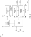
- FIG. 2 shows a block diagram circuit configuration 200 according to examples of the present disclosure.
- the circuit comprises timing circuit 202 that has two inputs, namely clock signal input 204 and reset input 206.
- Output from timing circuit 202 is provided to coupling generator (aggressor) 208, which biases a first communication transmission line with a current ramp signal, as discussed further below.
- Output from coupling generator (aggressor) 208 is provided to coupling interconnect (DUI) 210.
- DI coupling interconnect
- Output from coupling interconnect (DUI) which represents the induced voltage to the victim line, is provided to sample and hold circuit 212.
- Output from sample and hold circuit 212 is provided to integrator and comparator 214.
- Output from integrator and comparator 214 is provided to 10-bit counter 216. Output from 10-bit counter 216 is D out .Output from timing circuit 202 is also provided to sample and hold circuit 212, integrator and comparator 214, and 10-bit counter 216. Counter 216 counts a number of cycles required to cross the known threshold to infer a mutual inductance between a first communication transmission line and a second communication transmission line.
- FIG. 3 shows an example circuit configuration 300 of FIG. 2 according to examples of the present disclosure.
- an aggressor signal 302 generated by coupling generator 303 such as coupling generator as shown in FIG. 4 , is provided to receive end 304 of first communication transmission line 306 (e.g., aggressor line).
- the aggressor signal 302 is a periodic analog current ramp signal.
- First communication transmission line 306 is near second communication transmission line 308 (e.g., victim line) in a parallel arrangement.
- Mutual inductance 310 denoted by L DUT , between first communication transmission line 306 and second communication transmission line 308 is measured by using a switched measurement architecture at transit end 312 of second communication transmission line 308.
- Aggressor signal 302 induces an electromotive force (emf) in second communication line 308 (e.g., victim line), wherein the voltage is sampled through onto a sampling capacitor.
- emf electromotive force
- the signal output at transmit end 312 of victim line 308 is provided to switch 314 that is operated according to first timing signal denoted by ⁇ 1 , switch 316 that is operated according to second timing signal denoted by ⁇ 2 , capacitor 318, denoted by C sample , switch 320 that is operated according to first timing signal denoted by ⁇ 1 , and switch 322 that is operated according to second timing signal denoted by ⁇ 2 .
- Capacitor 318, denoted by C sample is charged when switch 314 is closed according to first timing signal, denoted by ⁇ 1 , and switch 316 is closed according to second timing signal, denoted by ⁇ 2 .
- switch 314 When switch 314 is closed according to first timing signal, denoted by ⁇ 1 , switch 316 is closed according to second timing signal, denoted by ⁇ 2 , switch 320 is closed according to first timing signal, denoted by ⁇ 1 , and switch 322 is closed according to second timing signal, denoted by ⁇ 2 , the signal is provided to switched capacitance integrator 324 that comprises amplifier 326, switch 328 that is operated according to reset timing signal, denoted by ⁇ Reset , and capacitor 330, denoted by C int .
- Capacitor 330 denoted by C int , is charged when switch 328 is closed according to reset timing signal, denoted by ⁇ Reset .
- switch 314, switch 316, capacitor 318, switch 320 comprise sample and hold circuit 212 and switch 322, switched capacitance integrator 324, amplifier 326, switch 328, and comparator 332 comprise integrator and comparator 214.
- FIG. 4 shows an example coupling generator 400 of the coupling generator FIG. 3 according to examples of the present disclosure.
- Coupling generator 400 uses a DC current source 402 and capacitor 406 to generate a linear voltage ramp and uses op-amp feedback circuit 48 to perform a voltage-to-current conversion to generate a current ramp signal (as shown in FIG. 5 ).
- DC current source 402 produces a direct current that charges capacitor 406 that produces a linear voltage ramp signal, which is used by op-amp feedback circuit 408 and first transistor 410 and second transistor, which can be P-type metal-oxide-semiconductor logic (PMOS or pMOS) field-effect transistors (FETs) that are configured to function as variable current sources, and resistor 414 to perform the voltage-to-current conversion to generate the current ramp signal that is outputted current ramp output, as denoted by I out 416.
- PMOS P-type metal-oxide-semiconductor logic
- FETs field-effect transistors
- FIG. 5 shows a current ramp signal 500 according to example of the present disclosure.
- V Lm(dI/dt)
- the voltage is captured and averaged multiple times through a switch capacitor integrator circuit.
- the operations of FIG. 3 run until the integrated voltage crosses a known reference and trips a dynamic latched comparator executed by comparator 332.
- the correlated double sampling techniques from the CBCM can be used in a similar fashion to remove charge injection, op-amp flicker noise, etc.
- Bias network e.g., first communication transmission line 306 and second communication transmission line 308 of FIG. 3 , forces switched capacitance integrator 324 to track a linear voltage ramp at coupling generator 303.
- examples in accordance with the present architecture can be integrated in a number of parallel interconnect in an embedded environment. Since the measurement circuit is near-DC, an insitu topology can be used with one measurement circuit that multiplexes the aggressor and victim nodes to any possible combination of parallel interconnects.
- FIG. 6 shows a plot of voltage versus time for the voltage induced in the victim line 308 from the aggressor line 306 according to examples of the present disclosure.
- a step current as shown in FIG. 6 , with the same amplitude can be applied. From low to high, the mutual inductance will induce a high voltage, beginning at T0, but it will settle to zero quickly, beginning at T1. The voltage remaining will be almost but not exactly equal to the capacitive voltage induced during ramp current.
- FIG. 7 shows a diagram for generating the voltage induced in the victim line 700 according to examples of the present disclosure.
- an aggressor signal 702 such as the signals shown in FIG. 6
- a coupling generator such as coupling generator as shown in FIG. 4
- Aggressor line 306 is near victim line 308 in a parallel arrangement. The signal is then outputted at transmit end 312 of victim line 308.
- FIG. 8 shows another example circuit configuration 800 of FIG. 2 according to examples of the present disclosure.
- an aggressor signal 302 generated by a coupling generator such as coupling generator as shown in FIG. 4
- receive end 304 of aggressor line 306 is provided to receive end 304 of aggressor line 306.
- Aggressor line 306 is near victim line 308 in a parallel arrangement.
- Mutual inductance 310, denoted by L DUT between aggressor line 306 and victim line 308 is measured by using a switched measurement architecture at transit end 312 of victim line 308.
- the signal output at transmit end 312 of victim line 308 is provided to switch 802 that is operated according to first timing signal, denoted by ⁇ 1 , and switch 804 that is operated according to third timing signal, denoted by ⁇ 3 .
- Capacitor 806, denoted by C s 1 is charged when switch 802 is closed according to first timing signal, denoted by ⁇ 1
- capacitor 808, denoted by C s 2 is charged when switch 804 is closed according to second timing signal, denoted by ⁇ 2 .
- switch 802 is closed according to first timing signal, denoted by ⁇ 1
- switch 804 is closed according to third timing signal, denoted by ⁇ 3
- a voltage is provided to switch 810 that is operated according to fourth timing signal, denoted by ⁇ 4
- switch 812 that is operated according to fourth timing signal, denoted by ⁇ 4 , respectively.
- switch 802 When switch 802 is closed according to first timing signal, denoted by ⁇ 1 , and switch 804 is closed according to second timing signal, denoted by ⁇ 2 a voltage is provided to switch 810, that is operated according to fourth timing signal, denoted by ⁇ 4 , and switch 812 that is operated by fourth timing signal, denoted by ⁇ 4 , respectively.
- switch 802 When switch 802 is closed according to first timing signal, denoted by ⁇ 1 , switch 804 is closed according to third timing signal, denoted by ⁇ 3 , switch 810 is closed according to fourth timing signal, denoted by ⁇ 4 , switch 812 is closed according to fourth timing signal, denoted by ⁇ 4 , and switch 814 is closed according to fourth timing signal, denoted by ⁇ 4 , a voltage is provided to differential switched capacitive integrator 816 that is operated according to reset timing signal, denoted by ⁇ Reset , and feedback capacitor 822, denoted by C int . Feedback capacitor 822, denoted by C int , is charged when switch 820 is closed according to reset timing signal, denoted by ⁇ Reset .
- differential switched capacitance integrator 816 The output of differential switched capacitance integrator 816 is provided to comparator 824.
- switch 802, switch 804, capacitor 806, capacitor 808 comprise sample and hold circuit 212 and switch 810
- switch 812, switch 814, amplifier 818, switch 820, and feedback capacitor 822 comprise differential switched capacitor integrator 816.
- Switch 810, switch 812, switch 814, amplifier 818, switch 820, feedback capacitor 822, and comparator 824 comprise integrator and comparator 214.
- FIG. 9 shows a timing diagram for FIG. 8 , which shows an interleaved current signal for when the various switches are operated according to first timing signal, denoted by ⁇ 1 , second timing signal, denoted by ⁇ 2 , third timing signal, denoted by ⁇ 3 , and fourth timing signal, denoted by ⁇ 4 .
- first timing signal denoted by ⁇ 1
- second timing signal denoted by ⁇ 2
- third timing signal denoted by ⁇ 3
- fourth timing signal denoted by ⁇ 4 .
- FIG. 10 shows a current signal generator 1000 according to examples of the present disclosure.
- switch 1002 and switch 1004 are closed, capacitor 1006 is charged.
- switch 1002, switch 1004, switch 1008, and switch 1010, PMOS 1012 and PMOS 1014 provide an input signal to amplifier 1018 that outputs an output signal to PMOS 1016, where the output signal is representative to a voltage by inductance coupling that is proportional to the slope of the ramp current.
- a current source with 1 mA peak to peak amplitude and 400 ns was able to create a detectable voltage in the victim line with length of as small as a few 100 ⁇ m.
- the current source needed to be designed to provide minimum 1mA peak to peak current and with a period of 400 ns.
- the current reference that has been used in this current signal generator is PTAT to cancel out the CTAT property of the circuit. This will make sure that the peak-to-peak current is constant with temperature variation.
- FIG. 11 shows a method 1100 to determine a mutual inductance between first communication line 306 and second communication line 308.
- Method 1100 comprising providing periodic coupling current ramp signal 302 to first communication transmission line 306 that induces a voltage on a nearby second communication transmission line 308 wherein the voltage is sampled and held on switched capacitance integrator 324, as in 1102.
- Method 1100 continues by integrating the voltage onto a feedback capacitor 330 of comparator 332 of switched capacitance integrator 324 when the charge is positive due to a positive change in voltage of the periodic digital signal on first communication transmission line 306, as in 1104.
- Method 1100 continues by integrating the voltage until it crosses a known threshold as measured on comparator 332, as in 1106.
- Method 1100 continues by counting, by counter 216, a number of cycles required to cross the known threshold to infer a mutual inductance between first communication transmission line 306 and second communication transmission line 308, as in 1108.
- Method 1100 can continue prior to the providing periodic coupling current ramp signal 302 as in 1102, method 1100 comprises resetting switched capacitance integrator 324 by closing and reopening switch 328 in parallel with switched capacitance integrator 324, as in 1110.
- Method 1100 can continue by receiving, at a processor, an output from the voltage comparator circuit and determining a capacitive-based coupling, as in 1112.
- FIG. 12 shows a method 1200 to determine a mutual inductance between a first communication line and a second communication line according to examples of the present disclosure.
- Method 1200 comprises providing a periodic coupling current ramp signal to a first communication transmission line (306) that induces a voltage on a nearby second communication transmission line (308), wherein the voltage is sampled and held on a first capacitive storage element (806), as in 1202.
- Method 1200 continues by providing a periodic current pulse signal to a first communication line (306) that capacitively couples a charge onto a nearby second communication transmission line (308), wherein a non-ideality of the charge that is capacitively coupled is sampled and held on a second capacitive storage element (808), as in 1204.
- Method 1200 continues by removing the charge that is capacitively coupled from a measurement through a differential switched capacitor integrator (816), as in 1206. Method continues by integrating the voltage onto a feedback capacitor (822) of a differential switched capacitor integrator (816) when the charge is positive due to a positive change in voltage of the periodic coupling ramp signal on the first communication transmission line (306), as in 1208. Method 1200 continues by integrating the voltage until it crosses a known threshold as measured on a comparator (824), as in 1210. Method 1200 continues by counting, by counter 216, a number of cycles required to cross the known threshold to infer a mutual inductance between the first communication transmission line (306) and the second communication transmission line (308), as in 1212.
- method 1200 comprises, wherein prior to the providing the periodic coupling ramp signal, the method comprises resetting the switched capacitor integrator (324) by closing and reopening a switch (328) in parallel with the switched capacitive integrator (324), as in 1214.
- any of the methods of the present disclosure may be executed by a computing system.
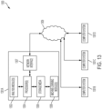
- FIG. 13 illustrates an example of such a computing system 1300, in accordance with some examples.
- the computing system 1300 may include a computer or computer system 1301A, which may be an individual computer system 1301A or an arrangement of distributed computer systems.
- the computer system 1301A includes one or more analysis module(s) 1302 configured to perform various tasks according to some examples, such as one or more methods disclosed herein. To perform these various tasks, the analysis module 1302 executes independently, or in coordination with, one or more hardware processors 1304, which is (or are) connected to one or more non-transitory computer readable medium 1306, such as a computer storage media.
- the hardware processor(s) 1304 is (or are) also connected to a network interface 1307 to allow the computer system 1301A to communicate over a data network 1309 with one or more additional computer systems and/or computing systems, such as 1301B, 1301C, and/or 1301D (note that computer systems 1301B, 1301C and/or 1301D may or may not share the same architecture as computer system 1301A, and may be located in different physical locations, e.g., computer systems 1301A and 1301B may be located in a processing facility, while in communication with one or more computer systems such as 1301C and/or 1301D that are located in one or more data centers, and/or located in varying countries on different continents).
- a processor can include a microprocessor, microcontroller, processor module or subsystem, programmable integrated circuit, programmable gate array, or another control or computing device.
- the non-transitory computer readable medium 1306 can be implemented as one or more computer-readable or machine-readable storage media.
- the non-transitory computer readable medium 1306 can be connected to or coupled with a machine learning module(s) 1308. Note that while in the example of FIG. 13 non-transitory computer readable medium 1306 is depicted as within computer system 1301A, in some examples, non-transitory computer readable medium 1306 may be distributed within and/or across multiple internal and/or external enclosures of computing system 1301A and/or additional computing systems.
- the non-transitory computer readable medium 1306 may include one or more different forms of memory including semiconductor memory devices such as dynamic or static random access memories (DRAMs or SRAMs), erasable and programmable read-only memories (EPROMs), electrically erasable and programmable read-only memories (EEPROMs) and flash memories, magnetic disks such as fixed, floppy and removable disks, other magnetic media including tape, optical media such as compact disks (CDs) or digital video disks (DVDs), BLURAY ® disks, or other types of optical storage, or other types of storage devices.
- semiconductor memory devices such as dynamic or static random access memories (DRAMs or SRAMs), erasable and programmable read-only memories (EPROMs), electrically erasable and programmable read-only memories (EEPROMs) and flash memories
- magnetic disks such as fixed, floppy and removable disks, other magnetic media including tape
- optical media such as compact disks (CDs) or digital video disks (DVDs),
- the instructions discussed above can be provided on one computer-readable or machine-readable storage medium, or alternatively, can be provided on multiple computer-readable or machine-readable storage media distributed in a large system having possibly plural nodes.
- Such computer-readable or machine-readable storage medium or media is (are) considered to be part of an article (or article of manufacture).
- An article or article of manufacture can refer to any manufactured single component or multiple components.
- the storage medium or media can be located either in the machine running the machine-readable instructions or located at a remote site from which machine-readable instructions can be downloaded over a network for execution.
- computer system 1300 (or computing system) is only one example of a computing system, and that computer system 1300 may have more or fewer components than shown, may combine additional components not depicted in the example of FIG. 13 , and/or computer system 1300 may have a different configuration or arrangement of the components depicted in FIG. 13 .
- the various components shown in FIG. 13 may be implemented in hardware, software, or a combination of both hardware and software, including one or more signal processing and/or application specific integrated circuits.
- the steps in the processing methods described herein may be implemented by running one or more functional modules in an information processing apparatus such as general purpose processors or application specific chips, such as application-specific integrated circuits (ASICs), field programmable gate arrays (FPGAs), or programmable logic devices (PLDs), or other appropriate devices.
- ASICs application-specific integrated circuits
- FPGAs field programmable gate arrays
- PLDs programmable logic devices
- Models and/or other interpretation aids may be refined in an iterative fashion; this concept is applicable to examples of the present methods discussed herein.
- This can include use of feedback loops executed on an algorithmic basis, such as at a computing device (e.g., computing system 1300, FIG. 13 ), and/or through manual control by a user who may make determinations regarding whether a given step, action, template, model, or set of curves has become sufficiently accurate for the evaluation of the signal(s) under consideration.
- a system for measuring mutual inductance between adjacent first communication transmission line and second communication transmission line comprising: a mutual inductance measurement circuit comprising: a coupling generator (208) which biases the first communication transmission line (306) with a current ramp signal (500); a sample and hold circuit (212) which captures an induced voltage on the second communication transmission line (308) using a switched capacitor storage element; a switched capacitor integrator configured to integrate the induced voltage onto an output voltage node; and a comparator (214) configured to switch states once the switched capacitor integration has surpassed a reference trippoint.
- a mutual inductance measurement circuit comprising: a coupling generator (208) which biases the first communication transmission line (306) with a current ramp signal (500); a sample and hold circuit (212) which captures an induced voltage on the second communication transmission line (308) using a switched capacitor storage element; a switched capacitor integrator configured to integrate the induced voltage onto an output voltage node; and a comparator (214) configured to switch states once the switched capacitor integration has surpassed a reference trip
- Clause 2 The system of clause 1, further comprising a coupling generator which utilizes a DC current source and a capacitor to generate a linear voltage ramp and an op-amp feedback circuit which performs voltage-to-current conversion to generate the current ramp signal.
- Clause 3 The system of clause 1 or clause 2, wherein the current ramp signal on the first communication transmission line induces a voltage on the second communication transmission line.
- Clause 4 The system of any of clauses 1-3, wherein the first communication transmission line is an aggressor line.
- Clause 5 The system of any of clauses 1-4, wherein the second communication transmission line is a victim line.
- Clause 6 The system of any of clauses 1-5, wherein the first communication transmission line and the second communication transmission line are high-speed analog communications channels.
- Clause 7 The system of any of clauses 1-6, wherein the first communication transmission line and the second communication transmission line are digital communications channels.
- Clause 9 The system of any of clauses 1-8, further comprising a processor configured to receive an output from the voltage comparator and determine the magnitude of mutual inductance.
- a method to determine a mutual inductance between a first communication transmission line and a second communication transmission line comprising: providing a periodic coupling current ramp signal to a first communication transmission line (306) that induces a voltage on a nearby second communication transmission line (308), wherein the voltage is sampled and held on a capacitor (318); integrating the voltage onto a feedback capacitor (330) of a switched capacitor integrator (324) when the charge is positive due to a positive change in voltage of the periodic coupling ramp signal on the first communication transmission line (306); integrating the voltage until it crosses a known threshold as measured on a comparator (332); and counting a number of cycles required to cross the known threshold to infer a mutual inductance between the first communication transmission line (306) and the second communication transmission line (308).
- Clause 12 The method of clause 11, wherein prior to the providing the periodic coupling ramp signal, the method comprises resetting the switched capacitor integrator (324) by closing and reopening a switch (328) in parallel with the switched capacitive integrator (324).
- Clause 13 The method of clause 11 or clause 12, wherein the first communication transmission line is an aggressor line.
- Clause 14 The method of any of clauses 11-13, wherein the second communication transmission line is a victim line.
- Clause 15 The method of any of clauses 11-14, wherein the first communication transmission line and the second communication transmission line are high-speed analog communications channels.
- Clause 16 The method of any of clauses 11-15, wherein the first communication transmission line and the second communication transmission line are digital communications channels.
- Clause 18 The method of any of clauses 11-17, further comprising receiving, at a processor, an output from the voltage comparator circuit and determining a capacitive-based coupling.
- a method to determine a mutual inductance between a first communication transmission line and a second communication transmission line comprising: providing a periodic coupling current ramp signal to a first communication transmission line (306) that induces a voltage on a nearby second communication transmission line (308), wherein the voltage is sampled and held on a first capacitive storage element (806); providing a periodic current pulse signal to a first communication transmission line (306) that capacitively couples a charge onto a nearby second communication transmission line (308), wherein a non-ideality of the charge that is capacitively coupled is sampled and held on a second capacitive storage element (808); removing the charge that is capacitively coupled from a measurement through a differential switched capacitor integrator (816); integrating the voltage onto a feedback capacitor (822) of a differential switched capacitor integrator (816) when the charge is positive due to a positive change in voltage of the periodic coupling ramp signal on the first communication transmission line (306); integrating the voltage until it crosses a known threshold as measured on a comparator (824
- Clause 20 The method of clause 19, wherein prior to the providing the periodic coupling ramp signal, the method comprises resetting the differential switched capacitor integrator (816) by closing and reopening a switch (820) in parallel with the capacitor integrator (822).
Landscapes
- Physics & Mathematics (AREA)
- General Physics & Mathematics (AREA)
- Engineering & Computer Science (AREA)
- Computer Networks & Wireless Communication (AREA)
- Signal Processing (AREA)
- Cable Transmission Systems, Equalization Of Radio And Reduction Of Echo (AREA)
- Semiconductor Integrated Circuits (AREA)
Abstract
Description
- This application is directed to methods and apparatus for in-situ measurement of mutual inductance between embedded interconnects.
- Mutual coupling/cross talk measurements are usually done with expensive test equipment that requires disconnecting signal wires from a system transmitter and receiver and connecting them to test equipment instead, and then reconnecting them back into the system. This approach tends to have many disadvantages including being both inefficient and time consuming.
- While several architectures exist for in-situ measurement of coupling capacitance (e.g. charge based capacitance measurement), we believe the following is first of its kind for discerning mutual inductance between coupled nodes/wires/interconnect in embedded environments.
- There is described herein a system for measuring mutual inductance between adjacent first communication transmission line and second communication transmission line is disclosed. The system comprises a mutual inductance measurement circuit comprising: a coupling generator (208) which biases the first communication transmission line (306) with a current ramp signal (500); a sample and hold circuit (212) which captures an induced voltage on the second communication transmission line (308) using a switched capacitor storage element; a switched capacitor integrator configured to integrate the induced voltage onto an output voltage node; and a comparator (214) configured to switch states once the switched capacitor integration has surpassed a reference trippoint.
- The system can include one or more of the following features. The system can further comprise a coupling generator which utilizes a DC current source and a capacitor to generate a linear voltage ramp and an op-amp feedback circuit which performs voltage-to-current conversion to generate the current ramp signal. The current ramp signal on the first communication transmission line induces a voltage on the second communication transmission line. The first communication transmission line is an aggressor line. The second communication transmission line is a victim line. The first communication transmission line and the second communication transmission line are high-speed analog communications channels. The first communication transmission line and the second communication transmission line are digital communications channels. The digital communications channels comprise application-specific integrated circuits (ASICs) or field programmable gate arrays (FPGAs). The system comprises a processor configured to receive an output from the voltage comparator and determine the magnitude of mutual inductance. The voltage comparator is a dynamic, clocked voltage comparator.
- There is described herein a method to determine a mutual inductance between a first communication transmission line and a second communication transmission line is disclosed. The method comprises providing a periodic coupling current ramp signal to a first communication transmission line that induces a voltage on a nearby second communication transmission line, wherein the voltage is sampled and held on a capacitor; integrating the voltage onto a feedback capacitor of a switched capacitor integrator when the charge is positive due to a positive change in voltage of the periodic coupling ramp signal on the first communication transmission line; integrating the voltage until it crosses a known threshold as measured on a comparator; and counting a number of cycles required to cross the known threshold to infer a mutual inductance between the first communication transmission line and the second communication transmission line.
- The method can include one or more the following features. Prior to the providing the periodic coupling ramp signal, the method comprises resetting the switched capacitor integrator by closing and reopening a switch in parallel with the switched capacitive integrator. The first communication transmission line is an aggressor line. The second communication transmission line is a victim line. The first communication transmission line and the second communication transmission line are high-speed analog communications channels. The first communication transmission line and the second communication transmission line are digital communications channels. The digital communications channels comprise application-specific integrated circuits (ASICs) or field programmable gate arrays (FPGAs). The method further comprising receiving, at a processor, an output from the voltage comparator circuit and determining a capacitive-based coupling.
- There is described herein a method to determine a mutual inductance between a first communication transmission line and a second communication transmission line is disclosed. The method comprising: providing a periodic coupling current ramp signal to a first communication transmission line that induces a voltage on a nearby second communication transmission line, wherein the voltage is sampled and held on a first capacitive storage element; providing a periodic current pulse signal to a first communication line that capacitively couples a charge onto a nearby second communication transmission line, wherein a non-ideality of the charge that is capacitively coupled is sampled and held on a second capacitive storage element; removing the charge that is capacitively coupled from a measurement through a differential switched capacitor integrator; integrating the voltage onto a feedback capacitor of a differential switched capacitor integrator when the charge is positive due to a positive change in voltage of the periodic coupling ramp signal on the first communication transmission line; integrating the voltage until it crosses a known threshold as measured on a comparator; and counting a number of cycles required to cross the known threshold to infer a mutual inductance between the first communication transmission line and the second communication transmission line. Prior to the providing the periodic coupling ramp signal, the method comprises resetting the differential switched capacitor integrator by closing and reopening a switch in parallel with the capacitor integrator.
-
-
FIG. 1 shows a conventional model for inductively coupled wires. -
FIG. 2 shows a block diagram circuit configuration according to examples of the present disclosure. -
FIG. 3 shows an example circuit configuration ofFIG. 2 according to examples of the present disclosure. -
FIG. 4 shows an example coupling generator circuit configuration of the coupling generatorFIG. 3 according to examples of the present disclosure. -
FIG. 5 shows a current ramp according to example of the present disclosure. -
FIG. 6 shows a plot of voltage versus time for the voltage induced in the victim line from the aggressor line according to examples of the present disclosure. -
FIG. 7 shows a diagram for generating the voltage induced in the victim line according to examples of the present disclosure. -
FIG. 8 shows another example circuit configuration ofFIG. 2 according to examples of the present disclosure. -
FIG. 9 shows a timing diagram forFIG. 9 , which shows an interleaved current signal for when switches are operated according to timing signals ϕ 1, ϕ 2, ϕ 3, ϕ 4 that determine the opening and closing of the respective switches according to examples of the present disclosure. -
FIG. 10 shows a current signal generator according to examples of the present disclosure. -
FIG. 11 show a flowchart for a method according to examples of the present disclosure. -
FIG. 12 shows a flowchart for a method to determine a mutual inductance between a first communication line and a second communication line according to examples of the present disclosure. -
FIG. 13 shows a computing system according to examples of the present disclosure. - Reference will now be made in detail to examples, some of which are illustrated in the accompanying drawings. Wherever possible, the same reference numbers will be used throughout the drawings to refer to the same or like parts.
- Generally speaking, examples of the present disclosure provide for a system, device, in-situ method for measuring mutual inductance between embedded interconnects. As opposed to a single shot measurement, the examples circuit architectures repeats the measurement numerous times and averages the result to improve measurement resolution and noise floor, relying on the fact that coupling properties are relatively static, i.e. low bandwidth. The architectures also leverage numerous forms of correlated double sampling and auto-zeroing to remove systematic artifacts and circuit non-idealities (e.g., capacitive coupling, amplifier offset voltage, switching injection noise, etc.). Also, examples of the present disclosure provide for the characterization of critical high-speed, high-density interconnect which cannot presently be characterized in their deeply embedded platform (e.g. 2.5D/3D advanced packaging systems). The example systems, devices, and methods are low power, low area, and scalable to many parallel interconnect- essentially providing this new characterization functionality with minimal disruption to existing system.
- The measurement operates on the simplest of principles, applying a steady ramp of current (dI/dt) to induce a voltage (V) on a coupled line with mutual inductance (LM) , as V = LM x dI/dt. Given a known current ramp, by taking a measurement of the induced voltage we can calculate the mutual inductance. The circuit architecture integrates the induced voltage over many discrete samples to improve measurement resolution and noise floor, and also leverages correlated double sampling to remove system artifacts.
-
FIG. 1 shows a model for inductively coupled wires. Any two communication transmission lines that are in vicinity of each other will be mutually coupled. This coupling effect can be both capacitive and inductive. Depending on the application, communication transmission lines need to be calibrated accurately where two coupled lines would have different impedance than each one separately. Tools like network analyzer can be used to calibrate the line however there are devices and applications that will be hard or impossible to calibrate the line using VNA. In this design the goal is to design an integrated circuit to calibrate the connection lines. - Based on the formula above, if a current is applied with constant rate of change the potential that will be built in the second line will be constant. This means that if we measure the voltage knowing the current rate of change the mutual inductance could be calculated. For this reason, a current ramp generator needs to be designed.
- If the induced voltage is measured, then the coupled inductance can be found as follows:


- The voltage induced is proportional to the current rate of change. To maximize the induced voltage we have to maximize the slope of the ramp current. This will result in limiting voltage that will be built on the victim line. For example, for a 1 nH coupled inductance, a current ramp with Imax = 1 mA and (T 1 - T 0) = 100 ns, the voltage that will be built in the victim line is 10 uV. This is too small to be measured directly therefore instead of measuring directly; using capacitor and integrator we can integrate charge for N cycles. A powerful thing about using an integrator is the fact that as the number of cycles goes up the signal to noise ratio will increase. This will help us to measure the voltage built in the victim line.
- Let say after N cycle the voltage built on integrator cap is Vsum then we have:





- Due to the ohmic impedance of the line it will build some potential differences between two lines. This means that some of the voltage in the victim line is due to capacitive coupling.
-
FIG. 2 shows a blockdiagram circuit configuration 200 according to examples of the present disclosure. As shown inFIG. 2 , the circuit comprisestiming circuit 202 that has two inputs, namelyclock signal input 204 and resetinput 206. Output fromtiming circuit 202 is provided to coupling generator (aggressor) 208, which biases a first communication transmission line with a current ramp signal, as discussed further below. Output from coupling generator (aggressor) 208 is provided to coupling interconnect (DUI) 210. Output from coupling interconnect (DUI), which represents the induced voltage to the victim line, is provided to sample and holdcircuit 212. Output from sample and holdcircuit 212 is provided to integrator andcomparator 214. Output from integrator andcomparator 214 is provided to 10-bit counter 216. Output from 10-bit counter 216 is Dout .Output fromtiming circuit 202 is also provided to sample and holdcircuit 212, integrator andcomparator 214, and 10-bit counter 216. Counter 216 counts a number of cycles required to cross the known threshold to infer a mutual inductance between a first communication transmission line and a second communication transmission line. -
FIG. 3 shows anexample circuit configuration 300 ofFIG. 2 according to examples of the present disclosure. As shown inFIG. 3 , anaggressor signal 302 generated bycoupling generator 303, such as coupling generator as shown inFIG. 4 , is provided to receiveend 304 of first communication transmission line 306 (e.g., aggressor line). For example, theaggressor signal 302 is a periodic analog current ramp signal. Firstcommunication transmission line 306 is near second communication transmission line 308 (e.g., victim line) in a parallel arrangement.Mutual inductance 310, denoted by LDUT, between firstcommunication transmission line 306 and secondcommunication transmission line 308 is measured by using a switched measurement architecture attransit end 312 of secondcommunication transmission line 308. Aggressor signal 302 induces an electromotive force (emf) in second communication line 308 (e.g., victim line), wherein the voltage is sampled through onto a sampling capacitor. - The signal output at transmit
end 312 ofvictim line 308 is provided to switch 314 that is operated according to first timing signal denoted by ϕ 1, switch 316 that is operated according to second timing signal denoted by ϕ 2,capacitor 318, denoted by Csample, switch 320 that is operated according to first timing signal denoted by ϕ 1, and switch 322 that is operated according to second timing signal denoted by ϕ 2.Capacitor 318, denoted by Csample, is charged whenswitch 314 is closed according to first timing signal, denoted by ϕ 1, and switch 316 is closed according to second timing signal, denoted by ϕ 2. Whenswitch 314 is closed according to first timing signal, denoted by ϕ 1,switch 316 is closed according to second timing signal, denoted by ϕ 2,switch 320 is closed according to first timing signal, denoted by ϕ 1, and switch 322 is closed according to second timing signal, denoted by ϕ 2, the signal is provided to switchedcapacitance integrator 324 that comprisesamplifier 326, switch 328 that is operated according to reset timing signal, denoted by ϕReset, andcapacitor 330, denoted by Cint. Capacitor 330, denoted by Cint, is charged whenswitch 328 is closed according to reset timing signal, denoted by ϕReset. The output of switchedcapacitance integrator 324 is provided tocomparator 332. In some examples including this example,switch 314,switch 316,capacitor 318, switch 320 comprise sample and holdcircuit 212 and switch 322, switchedcapacitance integrator 324,amplifier 326,switch 328, andcomparator 332 comprise integrator andcomparator 214. -
FIG. 4 shows anexample coupling generator 400 of the coupling generatorFIG. 3 according to examples of the present disclosure.Coupling generator 400 uses a DCcurrent source 402 andcapacitor 406 to generate a linear voltage ramp and uses op-amp feedback circuit 48 to perform a voltage-to-current conversion to generate a current ramp signal (as shown inFIG. 5 ). In operation, when switch 404 is closed, DCcurrent source 402 produces a direct current that chargescapacitor 406 that produces a linear voltage ramp signal, which is used by op-amp feedback circuit 408 andfirst transistor 410 and second transistor, which can be P-type metal-oxide-semiconductor logic (PMOS or pMOS) field-effect transistors (FETs) that are configured to function as variable current sources, andresistor 414 to perform the voltage-to-current conversion to generate the current ramp signal that is outputted current ramp output, as denoted byI out 416. -
FIG. 5 shows acurrent ramp signal 500 according to example of the present disclosure. Aggressor signal 302 generated by the coupling generator ofFIG. 3 , such as couplinggenerator circuit configuration 400, comprises a known linear ramp of current (dI/dt), such as shown inFIG. 5 , on anaggressor line 306 and switchedcapacitance integrator 324 measures the voltage developed on the nearby Victim line, governed by V = Lm(dI/dt). In order to improve measurement resolution, the voltage is captured and averaged multiple times through a switch capacitor integrator circuit. The operations ofFIG. 3 run until the integrated voltage crosses a known reference and trips a dynamic latched comparator executed bycomparator 332. Additionally, the correlated double sampling techniques from the CBCM can be used in a similar fashion to remove charge injection, op-amp flicker noise, etc. - Assuming
comparator 332 yield infinite resolution, the measurement noise floor would be limited by non-linearity in the current ramp circuit. Bias network, e.g., firstcommunication transmission line 306 and secondcommunication transmission line 308 ofFIG. 3 , forces switchedcapacitance integrator 324 to track a linear voltage ramp atcoupling generator 303. Also, examples in accordance with the present architecture can be integrated in a number of parallel interconnect in an embedded environment. Since the measurement circuit is near-DC, an insitu topology can be used with one measurement circuit that multiplexes the aggressor and victim nodes to any possible combination of parallel interconnects. -
FIG. 6 shows a plot of voltage versus time for the voltage induced in thevictim line 308 from theaggressor line 306 according to examples of the present disclosure. To calibrate the voltage that was built due to coupling capacitance, a step current, as shown inFIG. 6 , with the same amplitude can be applied. From low to high, the mutual inductance will induce a high voltage, beginning at T0, but it will settle to zero quickly, beginning at T1. The voltage remaining will be almost but not exactly equal to the capacitive voltage induced during ramp current. -
FIG. 7 shows a diagram for generating the voltage induced in thevictim line 700 according to examples of the present disclosure. As shown inFIG. 7 , an aggressor signal 702, such as the signals shown inFIG. 6 , is generated by a coupling generator, such as coupling generator as shown inFIG. 4 , is provided to receiveend 304 ofaggressor line 306.Aggressor line 306 is nearvictim line 308 in a parallel arrangement. The signal is then outputted at transmitend 312 ofvictim line 308. -
FIG. 8 shows anotherexample circuit configuration 800 ofFIG. 2 according to examples of the present disclosure. As shown inFIG. 8 , anaggressor signal 302 generated by a coupling generator, such as coupling generator as shown inFIG. 4 , is provided to receiveend 304 ofaggressor line 306.Aggressor line 306 is nearvictim line 308 in a parallel arrangement.Mutual inductance 310, denoted by LDUT, betweenaggressor line 306 andvictim line 308 is measured by using a switched measurement architecture attransit end 312 ofvictim line 308. The signal output at transmitend 312 ofvictim line 308 is provided to switch 802 that is operated according to first timing signal, denoted by ϕ 1, and switch 804 that is operated according to third timing signal, denoted by ϕ 3.Capacitor 806, denoted by C s1, is charged whenswitch 802 is closed according to first timing signal, denoted by ϕ 1, andcapacitor 808, denoted by C s2, is charged whenswitch 804 is closed according to second timing signal, denoted by ϕ 2. Whenswitch 802 is closed according to first timing signal, denoted by ϕ 1, and switch 804 is closed according to third timing signal, denoted by ϕ 3, a voltage is provided to switch 810 that is operated according to fourth timing signal, denoted by ϕ 4, and switch 812 that is operated according to fourth timing signal, denoted by ϕ 4, respectively. Whenswitch 802 is closed according to first timing signal, denoted by ϕ 1, and switch 804 is closed according to second timing signal, denoted by ϕ 2 a voltage is provided to switch 810, that is operated according to fourth timing signal, denoted by ϕ 4, and switch 812 that is operated by fourth timing signal, denoted by ϕ 4, respectively. Whenswitch 802 is closed according to first timing signal, denoted by ϕ 1,switch 804 is closed according to third timing signal, denoted by ϕ 3,switch 810 is closed according to fourth timing signal, denoted by ϕ 4,switch 812 is closed according to fourth timing signal, denoted by ϕ 4, and switch 814 is closed according to fourth timing signal, denoted by ϕ 4, a voltage is provided to differential switchedcapacitive integrator 816 that is operated according to reset timing signal, denoted by ϕReset, andfeedback capacitor 822, denoted by Cint. Feedback capacitor 822, denoted by Cint, is charged whenswitch 820 is closed according to reset timing signal, denoted by ϕReset. The output of differential switchedcapacitance integrator 816 is provided tocomparator 824. In some examples including this example,switch 802,switch 804,capacitor 806,capacitor 808 comprise sample and holdcircuit 212 and switch 810,switch 812,switch 814,amplifier 818,switch 820, andfeedback capacitor 822 comprise differential switchedcapacitor integrator 816.Switch 810,switch 812,switch 814,amplifier 818,switch 820,feedback capacitor 822, andcomparator 824 comprise integrator andcomparator 214. -
FIG. 9 shows a timing diagram forFIG. 8 , which shows an interleaved current signal for when the various switches are operated according to first timing signal, denoted by ϕ 1, second timing signal, denoted by ϕ 2, third timing signal, denoted by ϕ 3, and fourth timing signal, denoted by ϕ 4. One solution to the issues discussed above with relation toFIG. 6 , can be interleaving these two currents and subtracting the two voltages from each other. In some examples including this example, additional switches and capacitors are used to store each voltage separately, as shown inFIG. 8 . - Using ideal components, the circuit above was able to measure the coupled inductance. For coupled lines a two mutually coupled inductance with inductive coefficient of 1 being used. From experimental results, it is determined that there is a linear relationship between measured inductance and actual inductance. The difference between measured and actual inductance is not surprising because of using large transistors for switches which introduce parasitic caps and having non-zero impedance when turned on. The slope and offset that exist here are systematic errors which can be calibrated later.
-
FIG. 10 shows acurrent signal generator 1000 according to examples of the present disclosure. Whenswitch 1002 andswitch 1004 are closed,capacitor 1006 is charged. Whenswitch 1002,switch 1004,switch 1008, andswitch 1010,PMOS 1012 andPMOS 1014 provide an input signal toamplifier 1018 that outputs an output signal toPMOS 1016, where the output signal is representative to a voltage by inductance coupling that is proportional to the slope of the ramp current. After running some simulation on mutually coupled lines model from rfTlineLib in cadence, a current source with 1 mA peak to peak amplitude and 400 ns was able to create a detectable voltage in the victim line with length of as small as a few 100 µm. The current source needed to be designed to provide minimum 1mA peak to peak current and with a period of 400 ns. The current reference that has been used in this current signal generator is PTAT to cancel out the CTAT property of the circuit. This will make sure that the peak-to-peak current is constant with temperature variation. -
FIG. 11 shows amethod 1100 to determine a mutual inductance betweenfirst communication line 306 andsecond communication line 308.Method 1100 comprising providing periodic couplingcurrent ramp signal 302 to firstcommunication transmission line 306 that induces a voltage on a nearby secondcommunication transmission line 308 wherein the voltage is sampled and held on switchedcapacitance integrator 324, as in 1102. -
Method 1100 continues by integrating the voltage onto afeedback capacitor 330 ofcomparator 332 of switchedcapacitance integrator 324 when the charge is positive due to a positive change in voltage of the periodic digital signal on firstcommunication transmission line 306, as in 1104. -
Method 1100 continues by integrating the voltage until it crosses a known threshold as measured oncomparator 332, as in 1106. -
Method 1100 continues by counting, bycounter 216, a number of cycles required to cross the known threshold to infer a mutual inductance between firstcommunication transmission line 306 and secondcommunication transmission line 308, as in 1108. -
Method 1100 can continue prior to the providing periodic couplingcurrent ramp signal 302 as in 1102,method 1100 comprises resetting switchedcapacitance integrator 324 by closing and reopeningswitch 328 in parallel with switchedcapacitance integrator 324, as in 1110. -
Method 1100 can continue by receiving, at a processor, an output from the voltage comparator circuit and determining a capacitive-based coupling, as in 1112. -
FIG. 12 shows amethod 1200 to determine a mutual inductance between a first communication line and a second communication line according to examples of the present disclosure.Method 1200 comprises providing a periodic coupling current ramp signal to a first communication transmission line (306) that induces a voltage on a nearby second communication transmission line (308), wherein the voltage is sampled and held on a first capacitive storage element (806), as in 1202.Method 1200 continues by providing a periodic current pulse signal to a first communication line (306) that capacitively couples a charge onto a nearby second communication transmission line (308), wherein a non-ideality of the charge that is capacitively coupled is sampled and held on a second capacitive storage element (808), as in 1204.Method 1200 continues by removing the charge that is capacitively coupled from a measurement through a differential switched capacitor integrator (816), as in 1206. Method continues by integrating the voltage onto a feedback capacitor (822) of a differential switched capacitor integrator (816) when the charge is positive due to a positive change in voltage of the periodic coupling ramp signal on the first communication transmission line (306), as in 1208.Method 1200 continues by integrating the voltage until it crosses a known threshold as measured on a comparator (824), as in 1210.Method 1200 continues by counting, bycounter 216, a number of cycles required to cross the known threshold to infer a mutual inductance between the first communication transmission line (306) and the second communication transmission line (308), as in 1212. In some examples,method 1200 comprises, wherein prior to the providing the periodic coupling ramp signal, the method comprises resetting the switched capacitor integrator (324) by closing and reopening a switch (328) in parallel with the switched capacitive integrator (324), as in 1214. - In some examples, any of the methods of the present disclosure may be executed by a computing system.
FIG. 13 illustrates an example of such acomputing system 1300, in accordance with some examples. Thecomputing system 1300 may include a computer orcomputer system 1301A, which may be anindividual computer system 1301A or an arrangement of distributed computer systems. Thecomputer system 1301A includes one or more analysis module(s) 1302 configured to perform various tasks according to some examples, such as one or more methods disclosed herein. To perform these various tasks, theanalysis module 1302 executes independently, or in coordination with, one ormore hardware processors 1304, which is (or are) connected to one or more non-transitory computer readable medium 1306, such as a computer storage media. The hardware processor(s) 1304 is (or are) also connected to anetwork interface 1307 to allow thecomputer system 1301A to communicate over adata network 1309 with one or more additional computer systems and/or computing systems, such as 1301B, 1301C, and/or 1301D (note thatcomputer systems 1301B, 1301C and/or 1301D may or may not share the same architecture ascomputer system 1301A, and may be located in different physical locations, e.g.,computer systems - The non-transitory computer readable medium 1306 can be implemented as one or more computer-readable or machine-readable storage media. The non-transitory computer readable medium 1306 can be connected to or coupled with a machine learning module(s) 1308. Note that while in the example of
FIG. 13 non-transitory computer readable medium 1306 is depicted as withincomputer system 1301A, in some examples, non-transitory computer readable medium 1306 may be distributed within and/or across multiple internal and/or external enclosures ofcomputing system 1301A and/or additional computing systems. The non-transitory computer readable medium 1306 may include one or more different forms of memory including semiconductor memory devices such as dynamic or static random access memories (DRAMs or SRAMs), erasable and programmable read-only memories (EPROMs), electrically erasable and programmable read-only memories (EEPROMs) and flash memories, magnetic disks such as fixed, floppy and removable disks, other magnetic media including tape, optical media such as compact disks (CDs) or digital video disks (DVDs), BLURAY® disks, or other types of optical storage, or other types of storage devices. Note that the instructions discussed above can be provided on one computer-readable or machine-readable storage medium, or alternatively, can be provided on multiple computer-readable or machine-readable storage media distributed in a large system having possibly plural nodes. Such computer-readable or machine-readable storage medium or media is (are) considered to be part of an article (or article of manufacture). An article or article of manufacture can refer to any manufactured single component or multiple components. The storage medium or media can be located either in the machine running the machine-readable instructions or located at a remote site from which machine-readable instructions can be downloaded over a network for execution. - It should be appreciated that computer system 1300 (or computing system) is only one example of a computing system, and that
computer system 1300 may have more or fewer components than shown, may combine additional components not depicted in the example ofFIG. 13 , and/orcomputer system 1300 may have a different configuration or arrangement of the components depicted inFIG. 13 . The various components shown inFIG. 13 may be implemented in hardware, software, or a combination of both hardware and software, including one or more signal processing and/or application specific integrated circuits. - Further, the steps in the processing methods described herein may be implemented by running one or more functional modules in an information processing apparatus such as general purpose processors or application specific chips, such as application-specific integrated circuits (ASICs), field programmable gate arrays (FPGAs), or programmable logic devices (PLDs), or other appropriate devices. These modules, combinations of these modules, and/or their combination with general hardware are all included within the scope of the claims.
- Models and/or other interpretation aids may be refined in an iterative fashion; this concept is applicable to examples of the present methods discussed herein. This can include use of feedback loops executed on an algorithmic basis, such as at a computing device (e.g.,
computing system 1300,FIG. 13 ), and/or through manual control by a user who may make determinations regarding whether a given step, action, template, model, or set of curves has become sufficiently accurate for the evaluation of the signal(s) under consideration. - Examples of the disclosure can include one or more of the following clauses.
-
Clause 1. A system for measuring mutual inductance between adjacent first communication transmission line and second communication transmission line, the system comprising: a mutual inductance measurement circuit comprising: a coupling generator (208) which biases the first communication transmission line (306) with a current ramp signal (500); a sample and hold circuit (212) which captures an induced voltage on the second communication transmission line (308) using a switched capacitor storage element; a switched capacitor integrator configured to integrate the induced voltage onto an output voltage node; and a comparator (214) configured to switch states once the switched capacitor integration has surpassed a reference trippoint. - Clause 2. The system of
clause 1, further comprising a coupling generator which utilizes a DC current source and a capacitor to generate a linear voltage ramp and an op-amp feedback circuit which performs voltage-to-current conversion to generate the current ramp signal. - Clause 3. The system of
clause 1 or clause 2, wherein the current ramp signal on the first communication transmission line induces a voltage on the second communication transmission line. -
Clause 4. The system of any of clauses 1-3, wherein the first communication transmission line is an aggressor line. - Clause 5. The system of any of clauses 1-4, wherein the second communication transmission line is a victim line.
- Clause 6. The system of any of clauses 1-5, wherein the first communication transmission line and the second communication transmission line are high-speed analog communications channels.
-
Clause 7. The system of any of clauses 1-6, wherein the first communication transmission line and the second communication transmission line are digital communications channels. - Clause 8. The system of any of clauses 1-7, wherein the digital communications channels comprise application-specific integrated circuits (ASICs) or field programmable gate arrays (FPGAs).
- Clause 9. The system of any of clauses 1-8, further comprising a processor configured to receive an output from the voltage comparator and determine the magnitude of mutual inductance.
-
Clause 10. The system of any of clauses 1-9, wherein the voltage comparator is a dynamic, clocked voltage comparator. - Clause 11. A method to determine a mutual inductance between a first communication transmission line and a second communication transmission line, the method comprising: providing a periodic coupling current ramp signal to a first communication transmission line (306) that induces a voltage on a nearby second communication transmission line (308), wherein the voltage is sampled and held on a capacitor (318); integrating the voltage onto a feedback capacitor (330) of a switched capacitor integrator (324) when the charge is positive due to a positive change in voltage of the periodic coupling ramp signal on the first communication transmission line (306); integrating the voltage until it crosses a known threshold as measured on a comparator (332); and counting a number of cycles required to cross the known threshold to infer a mutual inductance between the first communication transmission line (306) and the second communication transmission line (308).
- Clause 12. The method of clause 11, wherein prior to the providing the periodic coupling ramp signal, the method comprises resetting the switched capacitor integrator (324) by closing and reopening a switch (328) in parallel with the switched capacitive integrator (324).
- Clause 13. The method of clause 11 or clause 12, wherein the first communication transmission line is an aggressor line.
- Clause 14. The method of any of clauses 11-13, wherein the second communication transmission line is a victim line.
- Clause 15. The method of any of clauses 11-14, wherein the first communication transmission line and the second communication transmission line are high-speed analog communications channels.
- Clause 16. The method of any of clauses 11-15, wherein the first communication transmission line and the second communication transmission line are digital communications channels.
- Clause 17. The method of any of clauses 11-16, wherein the digital communications channels comprise application-specific integrated circuits (ASICs) or field programmable gate arrays (FPGAs).
- Clause 18. The method of any of clauses 11-17, further comprising receiving, at a processor, an output from the voltage comparator circuit and determining a capacitive-based coupling.
- Clause 19. A method to determine a mutual inductance between a first communication transmission line and a second communication transmission line, the method comprising: providing a periodic coupling current ramp signal to a first communication transmission line (306) that induces a voltage on a nearby second communication transmission line (308), wherein the voltage is sampled and held on a first capacitive storage element (806); providing a periodic current pulse signal to a first communication transmission line (306) that capacitively couples a charge onto a nearby second communication transmission line (308), wherein a non-ideality of the charge that is capacitively coupled is sampled and held on a second capacitive storage element (808); removing the charge that is capacitively coupled from a measurement through a differential switched capacitor integrator (816); integrating the voltage onto a feedback capacitor (822) of a differential switched capacitor integrator (816) when the charge is positive due to a positive change in voltage of the periodic coupling ramp signal on the first communication transmission line (306); integrating the voltage until it crosses a known threshold as measured on a comparator (824); and counting a number of cycles required to cross the known threshold to infer a mutual inductance between the first communication transmission line (306) and the second communication transmission line (308).
- Clause 20. The method of clause 19, wherein prior to the providing the periodic coupling ramp signal, the method comprises resetting the differential switched capacitor integrator (816) by closing and reopening a switch (820) in parallel with the capacitor integrator (822).
- The foregoing description, for purpose of explanation, has been described with reference to specific examples. However, the illustrative discussions above are not intended to be exhaustive or to limit the scope of the claims to the precise forms disclosed. Many modifications and variations are possible in view of the above teachings. Moreover, the order in which the elements of the methods are illustrated and described may be re-arranged, and/or two or more elements may occur simultaneously. The examples were chosen and described in order to best explain the principles of this disclosure and its practical applications, to thereby enable others skilled in the art to best utilize this disclosure and various examples with various modifications as are suited to the particular use contemplated.
- Notwithstanding that the numerical ranges and parameters setting forth the broad scope of the examples are approximations, the numerical values set forth in the specific examples are reported as precisely as possible. Any numerical value, however, inherently contains certain errors necessarily resulting from the standard deviation found in their respective testing measurements. Moreover, all ranges disclosed herein are to be understood to encompass any and all sub-ranges subsumed therein. For example, a range of "less than 10" can include any and all sub-ranges between (and including) the minimum value of zero and the maximum value of 10, that is, any and all sub-ranges having a minimum value of equal to or greater than zero and a maximum value of equal to or less than 10, e.g., 1 to 5. In certain cases, the numerical values as stated for the parameter can take on negative values. In this case, the example value of range stated as "less than 10" can assume negative values, e.g. - 1, -2, -3, - 10, -20, -30, etc.
- The examples are described for illustrative purposes only with reference to the Figures. Those of skill in the art will appreciate that the description is exemplary in nature, and that various modifications to the parameters set forth herein could be made without departing from the scope of the claims. It is intended that the specification and examples be considered as examples only. The various examples are not necessarily mutually exclusive, as some examples can be combined with one or more other examples to form new examples .
- While the examples have been illustrated respect to one or more implementations, alterations and/or modifications can be made to the illustrated examples without departing from the scope of the appended claims. In addition, while a particular feature of the examples may have been disclosed with respect to only one of several examples, such feature may be combined with one or more other features of the other examples as may be desired and advantageous for any given or particular function.
- Furthermore, to the extent that the terms "including", "includes", "having", "has", "with", or variants thereof are used in either the detailed description and the claims, such terms are intended to be inclusive in a manner similar to the term "comprising." As used herein, the phrase "one or more of", for example, A, B, and C means any of the following: either A, B, or C alone; or combinations of two, such as A and B, B and C, and A and C; or combinations of A, B and C.
- Other examples will be apparent to those skilled in the art from consideration of the specification and practice of the descriptions disclosed herein. It is intended that the specification and examples be considered as exemplary only, with a true scope being indicated by the following claims.
Claims (15)
- A system for measuring mutual inductance between adjacent first communication transmission line and second communication transmission line, the system comprising:
a mutual inductance measurement circuit comprising:a coupling generator (208) which biases the first communication transmission line (306) with a current ramp signal (500);a sample and hold circuit (212) which captures an induced voltage on the second communication transmission line (308) using a switched capacitor storage element;a switched capacitor integrator configured to integrate the induced voltage onto an output voltage node; anda comparator (214) configured to switch states once the switched capacitor integration has surpassed a reference trippoint. - The system of claim 1, further comprising a coupling generator which utilizes a DC current source and a capacitor to generate a linear voltage ramp and an op-amp feedback circuit which performs voltage-to-current conversion to generate the current ramp signal.
- The system of claim 1 or 2, wherein the current ramp signal on the first communication transmission line induces a voltage on the second communication transmission line.
- The system of any of claims 1 to 3, wherein the first communication transmission line is an aggressor line or a victim line.
- The system of any of claims 1 to 4, wherein the first communication transmission line and the second communication transmission line are high-speed analog communications channels.
- The system of any of claims 1 to 5, wherein the first communication transmission line and the second communication transmission line are digital communications channels.
- The system of claim 6, wherein the digital communications channels comprise application-specific integrated circuits (ASICs) or field programmable gate arrays (FPGAs).
- The system of any of claims 1 to 7, further comprising a processor configured to receive an output from the comparator and determine the magnitude of mutual inductance.
- The system of any of claims 1 to 8, wherein the comparator is a dynamic, clocked voltage comparator.
- A method to determine a mutual inductance between a first communication transmission line and a second communication transmission line, the method comprising:providing a periodic coupling current ramp signal to a first communication transmission line (306) that induces a voltage on a nearby second communication transmission line (308), wherein the voltage is sampled and held on a capacitor (318);integrating the voltage onto a feedback capacitor (330) of a switched capacitor integrator (324) when the charge is positive due to a positive change in voltage of the periodic coupling ramp signal on the first communication transmission line (306);integrating the voltage until it crosses a known threshold as measured on a comparator (332); andcounting a number of cycles required to cross the known threshold to infer a mutual inductance between the first communication transmission line (306) and the second communication transmission line (308).
- The method of claim 10, wherein prior to the providing the periodic coupling ramp signal, the method comprises resetting the switched capacitor integrator (324) by closing and reopening a switch (328) in parallel with the switched capacitive integrator (324).
- The method of claim 10 or 11, wherein the first communication transmission line is an aggressor line or a victim line.
- The method of any of claims 10 to 12, wherein the first communication transmission line and the second communication transmission line are high-speed analog communications channels or digital communications channels.
- The method of claim 13, wherein the digital communications channels comprise application-specific integrated circuits (ASICs) or field programmable gate arrays (FPGAs).
- The method of any of claims 10 to 14, further comprising receiving, at a processor, an output from the voltage comparator circuit and determining a capacitive-based coupling.
Applications Claiming Priority (1)
| Application Number | Priority Date | Filing Date | Title |
|---|---|---|---|
| US18/498,899 US12625173B2 (en) | 2023-10-31 | 2023-10-31 | Methods and apparatus for in-situ measurement of mutual inductance between embedded interconnects |
Publications (1)
| Publication Number | Publication Date |
|---|---|
| EP4549963A1 true EP4549963A1 (en) | 2025-05-07 |
Family
ID=92538820
Family Applications (1)
| Application Number | Title | Priority Date | Filing Date |
|---|---|---|---|
| EP24196283.6A Pending EP4549963A1 (en) | 2023-10-31 | 2024-08-23 | Methods and apparatus for in-situ measurement of mututal inductance between embedded interconnects |
Country Status (2)
| Country | Link |
|---|---|
| US (1) | US12625173B2 (en) |
| EP (1) | EP4549963A1 (en) |
Families Citing this family (1)
| Publication number | Priority date | Publication date | Assignee | Title |
|---|---|---|---|---|
| US12395206B2 (en) * | 2023-10-09 | 2025-08-19 | The Boeing Company | Parasitic tolerant charge-based coupling measurement |
Citations (6)
| Publication number | Priority date | Publication date | Assignee | Title |
|---|---|---|---|---|
| US20040019864A1 (en) * | 2002-07-29 | 2004-01-29 | Ghun Kim | Method and apparatus for analyzing inductive effects in a circuit layout |
| US7337419B2 (en) * | 2004-07-29 | 2008-02-26 | Stmicroelectronics, Inc. | Crosstalk noise reduction circuit and method |
| US20110069782A1 (en) * | 2008-07-02 | 2011-03-24 | Rambus Inc. | Capacitive-coupled Crosstalk Cancellation |
| US8214781B1 (en) * | 2008-09-10 | 2012-07-03 | Altera Corporation | Empirical prediction of simultaneous switching noise |
| US9503155B2 (en) * | 2015-04-09 | 2016-11-22 | Nxp B.V. | Tuning asymmetry of a differential digital interface to cancel magnetic coupling |
| US10771108B1 (en) * | 2019-12-17 | 2020-09-08 | Cadence Design Systems, Inc. | Crosstalk cancellation in a receiver |
Family Cites Families (30)
| Publication number | Priority date | Publication date | Assignee | Title |
|---|---|---|---|---|
| US3665458A (en) | 1970-05-14 | 1972-05-23 | Boeing Co | Capacitor ladder network |
| US5339041A (en) | 1993-07-06 | 1994-08-16 | The Boeing Company | High efficiency power amplifier |
| US6411108B1 (en) | 1999-11-05 | 2002-06-25 | Sensor Technologies, Inc. | Noncontact signal analyzer |
| DE10001129A1 (en) | 2000-01-13 | 2001-07-26 | Infineon Technologies Ag | Circuit arrangement for measuring the capacitance of structures in an integrated circuit |
| US6611148B2 (en) | 2001-07-24 | 2003-08-26 | Henry H. Clinton | Apparatus for the high voltage testing of insulated conductors and oscillator circuit for use with same |
| US6700399B1 (en) | 2002-12-12 | 2004-03-02 | Texas Instruments Incorporated | High density parasitic measurement structure |
| JP4342959B2 (en) | 2003-01-21 | 2009-10-14 | 株式会社ルネサステクノロジ | Capacitance value measurement circuit and wiring characteristic analysis method |
| US7349471B2 (en) | 2003-11-19 | 2008-03-25 | The Boeing Company | PPM receiving system and method using time-interleaved integrators |
| US7067842B1 (en) | 2004-02-13 | 2006-06-27 | Altera Corporation | Method and apparatus for monitoring parasitic inductance |
| US7639001B2 (en) | 2006-01-17 | 2009-12-29 | The Boeing Company | Built-in test for high speed electrical networks |
| US8253392B2 (en) | 2007-02-23 | 2012-08-28 | Compagnie General Desesta Blissements Michelin | Method for discharging capacitive loads |
| US9871293B2 (en) | 2010-11-03 | 2018-01-16 | The Boeing Company | Two-dimensionally electronically-steerable artificial impedance surface antenna |
| US8638105B2 (en) | 2010-11-09 | 2014-01-28 | The Boeing Company | Cell telemetry sample and hold amplifier |
| EP2795350B1 (en) | 2011-12-23 | 2015-11-25 | Imec | Method and system for measuring capacitance difference between capacitive elements |
| US9793220B2 (en) | 2012-03-16 | 2017-10-17 | Intel Deutschland Gmbh | Detection of environmental conditions in a semiconductor chip |
| EP2838421B1 (en) | 2012-04-16 | 2019-05-29 | ICU Medical, Inc. | Medical cable including authentication circuit |
| JP2015070195A (en) | 2013-09-30 | 2015-04-13 | ソニー株式会社 | Semiconductor device and test method |
| JP6519972B2 (en) | 2014-02-07 | 2019-05-29 | 株式会社リコー | High pass filter circuit and band pass filter circuit |
| US9602160B2 (en) * | 2014-10-23 | 2017-03-21 | Intel Corporation | Apparatus and method for digitally cancelling crosstalk |
| TWI720052B (en) | 2015-11-10 | 2021-03-01 | 美商Idac控股公司 | Wireless transmit/receive unit and wireless communication method |
| JP2017138130A (en) | 2016-02-01 | 2017-08-10 | ソニー株式会社 | Semiconductor integrated circuit and signal processing method |
| US10063077B2 (en) | 2016-03-28 | 2018-08-28 | The Boeing Company | System architecture for battery charger |
| EP3537336B1 (en) | 2017-11-07 | 2021-03-17 | Shenzhen Goodix Technology Co., Ltd. | Fingerprint sensor and terminal device |
| US10892911B2 (en) | 2018-08-28 | 2021-01-12 | Texas Instruments Incorporated | Controller area network receiver |
| US11029355B2 (en) | 2019-04-03 | 2021-06-08 | The Boeing Company | Direct measurement test structures for measuring static random access memory static noise margin |
| US11223368B1 (en) * | 2020-10-02 | 2022-01-11 | Cirrus Logic, Inc. | Inter-channel crosstalk and non-linearity reduction in double-sampled switched-capacitor delta-sigma data converters |
| US11608186B2 (en) | 2021-01-05 | 2023-03-21 | The Boeing Company | Impedance balancing for noise filtering in electric drive systems |
| IT202200019113A1 (en) | 2022-09-19 | 2024-03-19 | St Microelectronics Srl | Measuring system, related integrated circuit and process |
| US12068802B1 (en) | 2023-03-13 | 2024-08-20 | The Boeing Company | All-digital cross-channel coupling measurement |
| US12395206B2 (en) | 2023-10-09 | 2025-08-19 | The Boeing Company | Parasitic tolerant charge-based coupling measurement |
-
2023
- 2023-10-31 US US18/498,899 patent/US12625173B2/en active Active
-
2024
- 2024-08-23 EP EP24196283.6A patent/EP4549963A1/en active Pending
Patent Citations (6)
| Publication number | Priority date | Publication date | Assignee | Title |
|---|---|---|---|---|
| US20040019864A1 (en) * | 2002-07-29 | 2004-01-29 | Ghun Kim | Method and apparatus for analyzing inductive effects in a circuit layout |
| US7337419B2 (en) * | 2004-07-29 | 2008-02-26 | Stmicroelectronics, Inc. | Crosstalk noise reduction circuit and method |
| US20110069782A1 (en) * | 2008-07-02 | 2011-03-24 | Rambus Inc. | Capacitive-coupled Crosstalk Cancellation |
| US8214781B1 (en) * | 2008-09-10 | 2012-07-03 | Altera Corporation | Empirical prediction of simultaneous switching noise |
| US9503155B2 (en) * | 2015-04-09 | 2016-11-22 | Nxp B.V. | Tuning asymmetry of a differential digital interface to cancel magnetic coupling |
| US10771108B1 (en) * | 2019-12-17 | 2020-09-08 | Cadence Design Systems, Inc. | Crosstalk cancellation in a receiver |
Non-Patent Citations (4)
| Title |
|---|
| ARANI SINHA ET AL: "Validation and Test Issues Related to Noise Induced by Parasitic Inductances of VLSI Interconnects", IEEE TRANSACTIONS ON ADVANCED PACKAGING, IEEE SERVICE CENTER, PISCATAWAY, NJ, USA, vol. 25, no. 3, 1 August 2002 (2002-08-01), XP011068423, ISSN: 1521-3323 * |
| HAO YU ET AL: "Staggered Twisted-Bundle Interconnect for Crosstalk and Delay Reduction", QUALITY OF ELECTRONIC DESIGN, 2005. ISQED 2005. SIXTH INTERNATIONAL SY MPOSIUM ON SAN JOSE, CA, USA 21-23 MARCH 2005, PISCATAWAY, NJ, USA,IEEE, 21 March 2005 (2005-03-21), pages 682 - 687, XP010782067, ISBN: 978-0-7695-2301-9, DOI: 10.1109/ISQED.2005.112 * |
| KAUSHIK B K ET AL: "An analytical approach to dynamic crosstalk in coupled interconnects", MICROELECTRONICS JOURNAL, MACKINTOSH PUBLICATIONS LTD. LUTON, GB, vol. 41, no. 2-3, 1 February 2010 (2010-02-01), pages 85 - 92, XP026940899, ISSN: 0026-2692, [retrieved on 20100206], DOI: 10.1016/J.MEJO.2009.12.011 * |
| OGASAHARA Y ET AL: "Measurement and Analysis of Inductive Coupling Noise in 90 nm Global Interconnects", IEEE JOURNAL OF SOLID-STATE CIRCUITS, IEEE, USA, vol. 43, no. 3, 1 March 2008 (2008-03-01), pages 718 - 728, XP011204873, ISSN: 0018-9200 * |
Also Published As
| Publication number | Publication date |
|---|---|
| US12625173B2 (en) | 2026-05-12 |
| US20250138071A1 (en) | 2025-05-01 |
Similar Documents
| Publication | Publication Date | Title |
|---|---|---|
| US7253680B2 (en) | Amplifier system with current-mode servo feedback | |
| US6597183B1 (en) | Resistance measurement system | |
| US20040183560A1 (en) | Method and integrated circuit for capacitor measurement with digital readout | |
| WO2017151982A1 (en) | High-resolution power electronics measurements | |
| EP3402079A1 (en) | Analog-to-digital converter, measurement arrangement and method for analog-to-digital conversion | |
| US20050229053A1 (en) | Circuit and method for low frequency testing of high frequency signal waveforms | |
| US20080297175A1 (en) | Apparatus and method for measuring capacitance to ground of conductor | |
| CN110890867B (en) | Amplifier | |
| EP4539346A1 (en) | Parasitic tolerant charge-based coupling measurement | |
| US9977088B2 (en) | Battery fuel gauge current sensing circuit and method thereof | |
| CN104169728B (en) | Method and system for measuring capacitance difference between capacitive elements | |
| US12625173B2 (en) | Methods and apparatus for in-situ measurement of mutual inductance between embedded interconnects | |
| US9438262B1 (en) | Method for testing differential analog-to-digital converter and system therefor | |
| US10955462B2 (en) | Apparatus and method for frequency characterization of an electronic system | |
| Jeong et al. | Built-in self-test for stability measurement of low dropout regulator | |
| Provost et al. | Auto-calibrating analog timer for on-chip testing | |
| US20090093987A1 (en) | Method for accurate measuring stray capacitance of automatic test equipment and system thereof | |
| US7235962B2 (en) | Inductor-based current sensing | |
| US20120025847A1 (en) | Method and sytem for measuring a time constant of an integrated circuit, and integrated circuit provided with such a system | |
| RU2693647C1 (en) | Integrating analog-to-digital converter for measuring small electrical signals | |
| US20190094261A1 (en) | Differential charge transfer based accelerometer | |
| CN105548651B (en) | Measuring device | |
| JPH05266687A (en) | Dynamic bias circuit for signal sampler | |
| JP4280915B2 (en) | Current-voltage conversion circuit | |
| CN103472288A (en) | Peak voltage detection circuit |
Legal Events
| Date | Code | Title | Description |
|---|---|---|---|
| PUAI | Public reference made under article 153(3) epc to a published international application that has entered the european phase |
Free format text: ORIGINAL CODE: 0009012 |
|
| STAA | Information on the status of an ep patent application or granted ep patent |
Free format text: STATUS: THE APPLICATION HAS BEEN PUBLISHED |
|
| AK | Designated contracting states |
Kind code of ref document: A1 Designated state(s): AL AT BE BG CH CY CZ DE DK EE ES FI FR GB GR HR HU IE IS IT LI LT LU LV MC ME MK MT NL NO PL PT RO RS SE SI SK SM TR |
|
| STAA | Information on the status of an ep patent application or granted ep patent |
Free format text: STATUS: REQUEST FOR EXAMINATION WAS MADE |
|
| 17P | Request for examination filed |
Effective date: 20251001 |
|
| GRAP | Despatch of communication of intention to grant a patent |
Free format text: ORIGINAL CODE: EPIDOSNIGR1 |
|
| STAA | Information on the status of an ep patent application or granted ep patent |
Free format text: STATUS: GRANT OF PATENT IS INTENDED |
|
| RIC1 | Information provided on ipc code assigned before grant |
Ipc: G01R 27/26 20060101AFI20260105BHEP Ipc: G01R 27/32 20060101ALI20260105BHEP Ipc: G01R 31/58 20200101ALI20260105BHEP Ipc: H04B 3/487 20150101ALI20260105BHEP Ipc: H04B 3/46 20150101ALI20260105BHEP |
|
| INTG | Intention to grant announced |
Effective date: 20260120 |
|
| P01 | Opt-out of the competence of the unified patent court (upc) registered |
Free format text: CASE NUMBER: UPC_APP_0003809_4549963/2026 Effective date: 20260202 |
|
| GRAS | Grant fee paid |
Free format text: ORIGINAL CODE: EPIDOSNIGR3 |
|
| GRAA | (expected) grant |
Free format text: ORIGINAL CODE: 0009210 |
|
| STAA | Information on the status of an ep patent application or granted ep patent |
Free format text: STATUS: THE PATENT HAS BEEN GRANTED |