EP4549919A1 - X-ray inspection system for inspection of an object - Google Patents
X-ray inspection system for inspection of an object Download PDFInfo
- Publication number
- EP4549919A1 EP4549919A1 EP24208471.3A EP24208471A EP4549919A1 EP 4549919 A1 EP4549919 A1 EP 4549919A1 EP 24208471 A EP24208471 A EP 24208471A EP 4549919 A1 EP4549919 A1 EP 4549919A1
- Authority
- EP
- European Patent Office
- Prior art keywords
- ray
- separate
- ray source
- inspection system
- roi
- Prior art date
- Legal status (The legal status is an assumption and is not a legal conclusion. Google has not performed a legal analysis and makes no representation as to the accuracy of the status listed.)
- Pending
Links
Images




Classifications
-
- G—PHYSICS
- G01—MEASURING; TESTING
- G01N—INVESTIGATING OR ANALYSING MATERIALS BY DETERMINING THEIR CHEMICAL OR PHYSICAL PROPERTIES
- G01N23/00—Investigating or analysing materials by the use of wave or particle radiation, e.g. X-rays or neutrons, not covered by groups G01N3/00 – G01N17/00, G01N21/00 or G01N22/00
- G01N23/02—Investigating or analysing materials by the use of wave or particle radiation, e.g. X-rays or neutrons, not covered by groups G01N3/00 – G01N17/00, G01N21/00 or G01N22/00 by transmitting the radiation through the material
- G01N23/06—Investigating or analysing materials by the use of wave or particle radiation, e.g. X-rays or neutrons, not covered by groups G01N3/00 – G01N17/00, G01N21/00 or G01N22/00 by transmitting the radiation through the material and measuring the absorption
- G01N23/083—Investigating or analysing materials by the use of wave or particle radiation, e.g. X-rays or neutrons, not covered by groups G01N3/00 – G01N17/00, G01N21/00 or G01N22/00 by transmitting the radiation through the material and measuring the absorption the radiation being X-rays
-
- G—PHYSICS
- G01—MEASURING; TESTING
- G01N—INVESTIGATING OR ANALYSING MATERIALS BY DETERMINING THEIR CHEMICAL OR PHYSICAL PROPERTIES
- G01N23/00—Investigating or analysing materials by the use of wave or particle radiation, e.g. X-rays or neutrons, not covered by groups G01N3/00 – G01N17/00, G01N21/00 or G01N22/00
- G01N23/02—Investigating or analysing materials by the use of wave or particle radiation, e.g. X-rays or neutrons, not covered by groups G01N3/00 – G01N17/00, G01N21/00 or G01N22/00 by transmitting the radiation through the material
- G01N23/04—Investigating or analysing materials by the use of wave or particle radiation, e.g. X-rays or neutrons, not covered by groups G01N3/00 – G01N17/00, G01N21/00 or G01N22/00 by transmitting the radiation through the material and forming images of the material
-
- G—PHYSICS
- G01—MEASURING; TESTING
- G01N—INVESTIGATING OR ANALYSING MATERIALS BY DETERMINING THEIR CHEMICAL OR PHYSICAL PROPERTIES
- G01N23/00—Investigating or analysing materials by the use of wave or particle radiation, e.g. X-rays or neutrons, not covered by groups G01N3/00 – G01N17/00, G01N21/00 or G01N22/00
- G01N23/02—Investigating or analysing materials by the use of wave or particle radiation, e.g. X-rays or neutrons, not covered by groups G01N3/00 – G01N17/00, G01N21/00 or G01N22/00 by transmitting the radiation through the material
- G01N23/04—Investigating or analysing materials by the use of wave or particle radiation, e.g. X-rays or neutrons, not covered by groups G01N3/00 – G01N17/00, G01N21/00 or G01N22/00 by transmitting the radiation through the material and forming images of the material
- G01N23/044—Investigating or analysing materials by the use of wave or particle radiation, e.g. X-rays or neutrons, not covered by groups G01N3/00 – G01N17/00, G01N21/00 or G01N22/00 by transmitting the radiation through the material and forming images of the material using laminography or tomosynthesis
-
- G—PHYSICS
- G01—MEASURING; TESTING
- G01N—INVESTIGATING OR ANALYSING MATERIALS BY DETERMINING THEIR CHEMICAL OR PHYSICAL PROPERTIES
- G01N23/00—Investigating or analysing materials by the use of wave or particle radiation, e.g. X-rays or neutrons, not covered by groups G01N3/00 – G01N17/00, G01N21/00 or G01N22/00
- G01N23/02—Investigating or analysing materials by the use of wave or particle radiation, e.g. X-rays or neutrons, not covered by groups G01N3/00 – G01N17/00, G01N21/00 or G01N22/00 by transmitting the radiation through the material
- G01N23/04—Investigating or analysing materials by the use of wave or particle radiation, e.g. X-rays or neutrons, not covered by groups G01N3/00 – G01N17/00, G01N21/00 or G01N22/00 by transmitting the radiation through the material and forming images of the material
- G01N23/046—Investigating or analysing materials by the use of wave or particle radiation, e.g. X-rays or neutrons, not covered by groups G01N3/00 – G01N17/00, G01N21/00 or G01N22/00 by transmitting the radiation through the material and forming images of the material using tomography, e.g. computed tomography [CT]
-
- G—PHYSICS
- G01—MEASURING; TESTING
- G01N—INVESTIGATING OR ANALYSING MATERIALS BY DETERMINING THEIR CHEMICAL OR PHYSICAL PROPERTIES
- G01N23/00—Investigating or analysing materials by the use of wave or particle radiation, e.g. X-rays or neutrons, not covered by groups G01N3/00 – G01N17/00, G01N21/00 or G01N22/00
- G01N23/02—Investigating or analysing materials by the use of wave or particle radiation, e.g. X-rays or neutrons, not covered by groups G01N3/00 – G01N17/00, G01N21/00 or G01N22/00 by transmitting the radiation through the material
- G01N23/06—Investigating or analysing materials by the use of wave or particle radiation, e.g. X-rays or neutrons, not covered by groups G01N3/00 – G01N17/00, G01N21/00 or G01N22/00 by transmitting the radiation through the material and measuring the absorption
- G01N23/18—Investigating the presence of flaws defects or foreign matter
-
- G—PHYSICS
- G01—MEASURING; TESTING
- G01N—INVESTIGATING OR ANALYSING MATERIALS BY DETERMINING THEIR CHEMICAL OR PHYSICAL PROPERTIES
- G01N23/00—Investigating or analysing materials by the use of wave or particle radiation, e.g. X-rays or neutrons, not covered by groups G01N3/00 – G01N17/00, G01N21/00 or G01N22/00
- G01N23/22—Investigating or analysing materials by the use of wave or particle radiation, e.g. X-rays or neutrons, not covered by groups G01N3/00 – G01N17/00, G01N21/00 or G01N22/00 by measuring secondary emission from the material
- G01N23/225—Investigating or analysing materials by the use of wave or particle radiation, e.g. X-rays or neutrons, not covered by groups G01N3/00 – G01N17/00, G01N21/00 or G01N22/00 by measuring secondary emission from the material using electron or ion
- G01N23/2251—Investigating or analysing materials by the use of wave or particle radiation, e.g. X-rays or neutrons, not covered by groups G01N3/00 – G01N17/00, G01N21/00 or G01N22/00 by measuring secondary emission from the material using electron or ion using incident electron beams, e.g. scanning electron microscopy [SEM]
-
- H—ELECTRICITY
- H01—ELECTRIC ELEMENTS
- H01J—ELECTRIC DISCHARGE TUBES OR DISCHARGE LAMPS
- H01J3/00—Details of electron-optical or ion-optical arrangements common to two or more basic types of discharge tubes or lamps
- H01J3/26—Arrangements for deflecting ray or beam
-
- H—ELECTRICITY
- H01—ELECTRIC ELEMENTS
- H01J—ELECTRIC DISCHARGE TUBES OR DISCHARGE LAMPS
- H01J3/00—Details of electron-optical or ion-optical arrangements common to two or more basic types of discharge tubes or lamps
- H01J3/36—Arrangements for controlling the ray or beam after passing the main deflection system, e.g. for post-acceleration or post-concentration
-
- H—ELECTRICITY
- H01—ELECTRIC ELEMENTS
- H01J—ELECTRIC DISCHARGE TUBES OR DISCHARGE LAMPS
- H01J35/00—X-ray tubes
- H01J35/24—Tubes wherein the point of impact of the cathode ray on the anode or anticathode is movable relative to the surface thereof
- H01J35/30—Tubes wherein the point of impact of the cathode ray on the anode or anticathode is movable relative to the surface thereof by deflection of the cathode ray
-
- G—PHYSICS
- G01—MEASURING; TESTING
- G01N—INVESTIGATING OR ANALYSING MATERIALS BY DETERMINING THEIR CHEMICAL OR PHYSICAL PROPERTIES
- G01N2223/00—Investigating materials by wave or particle radiation
- G01N2223/10—Different kinds of radiation or particles
- G01N2223/101—Different kinds of radiation or particles electromagnetic radiation
- G01N2223/1016—X-ray
-
- G—PHYSICS
- G01—MEASURING; TESTING
- G01N—INVESTIGATING OR ANALYSING MATERIALS BY DETERMINING THEIR CHEMICAL OR PHYSICAL PROPERTIES
- G01N2223/00—Investigating materials by wave or particle radiation
- G01N2223/20—Sources of radiation
- G01N2223/204—Sources of radiation source created from radiated target
-
- G—PHYSICS
- G01—MEASURING; TESTING
- G01N—INVESTIGATING OR ANALYSING MATERIALS BY DETERMINING THEIR CHEMICAL OR PHYSICAL PROPERTIES
- G01N2223/00—Investigating materials by wave or particle radiation
- G01N2223/30—Accessories, mechanical or electrical features
- G01N2223/308—Accessories, mechanical or electrical features support of radiation source
-
- G—PHYSICS
- G01—MEASURING; TESTING
- G01N—INVESTIGATING OR ANALYSING MATERIALS BY DETERMINING THEIR CHEMICAL OR PHYSICAL PROPERTIES
- G01N2223/00—Investigating materials by wave or particle radiation
- G01N2223/30—Accessories, mechanical or electrical features
- G01N2223/316—Accessories, mechanical or electrical features collimators
-
- G—PHYSICS
- G01—MEASURING; TESTING
- G01N—INVESTIGATING OR ANALYSING MATERIALS BY DETERMINING THEIR CHEMICAL OR PHYSICAL PROPERTIES
- G01N2223/00—Investigating materials by wave or particle radiation
- G01N2223/30—Accessories, mechanical or electrical features
- G01N2223/33—Accessories, mechanical or electrical features scanning, i.e. relative motion for measurement of successive object-parts
- G01N2223/3306—Accessories, mechanical or electrical features scanning, i.e. relative motion for measurement of successive object-parts object rotates
-
- G—PHYSICS
- G01—MEASURING; TESTING
- G01N—INVESTIGATING OR ANALYSING MATERIALS BY DETERMINING THEIR CHEMICAL OR PHYSICAL PROPERTIES
- G01N2223/00—Investigating materials by wave or particle radiation
- G01N2223/30—Accessories, mechanical or electrical features
- G01N2223/33—Accessories, mechanical or electrical features scanning, i.e. relative motion for measurement of successive object-parts
- G01N2223/3307—Accessories, mechanical or electrical features scanning, i.e. relative motion for measurement of successive object-parts source and detector fixed; object moves
-
- G—PHYSICS
- G01—MEASURING; TESTING
- G01N—INVESTIGATING OR ANALYSING MATERIALS BY DETERMINING THEIR CHEMICAL OR PHYSICAL PROPERTIES
- G01N2223/00—Investigating materials by wave or particle radiation
- G01N2223/40—Imaging
- G01N2223/401—Imaging image processing
-
- G—PHYSICS
- G01—MEASURING; TESTING
- G01N—INVESTIGATING OR ANALYSING MATERIALS BY DETERMINING THEIR CHEMICAL OR PHYSICAL PROPERTIES
- G01N2223/00—Investigating materials by wave or particle radiation
- G01N2223/40—Imaging
- G01N2223/413—Imaging sensor array [CCD]
-
- G—PHYSICS
- G01—MEASURING; TESTING
- G01N—INVESTIGATING OR ANALYSING MATERIALS BY DETERMINING THEIR CHEMICAL OR PHYSICAL PROPERTIES
- G01N2223/00—Investigating materials by wave or particle radiation
- G01N2223/60—Specific applications or type of materials
- G01N2223/611—Specific applications or type of materials patterned objects; electronic devices
- G01N2223/6113—Specific applications or type of materials patterned objects; electronic devices printed circuit board [PCB]
-
- G—PHYSICS
- G01—MEASURING; TESTING
- G01N—INVESTIGATING OR ANALYSING MATERIALS BY DETERMINING THEIR CHEMICAL OR PHYSICAL PROPERTIES
- G01N2223/00—Investigating materials by wave or particle radiation
- G01N2223/60—Specific applications or type of materials
- G01N2223/611—Specific applications or type of materials patterned objects; electronic devices
- G01N2223/6116—Specific applications or type of materials patterned objects; electronic devices semiconductor wafer
-
- H—ELECTRICITY
- H01—ELECTRIC ELEMENTS
- H01J—ELECTRIC DISCHARGE TUBES OR DISCHARGE LAMPS
- H01J2235/00—X-ray tubes
- H01J2235/06—Cathode assembly
- H01J2235/068—Multi-cathode assembly
-
- H—ELECTRICITY
- H01—ELECTRIC ELEMENTS
- H01J—ELECTRIC DISCHARGE TUBES OR DISCHARGE LAMPS
- H01J35/00—X-ray tubes
- H01J35/02—Details
- H01J35/14—Arrangements for concentrating, focusing, or directing the cathode ray
- H01J35/153—Spot position control
-
- H—ELECTRICITY
- H05—ELECTRIC TECHNIQUES NOT OTHERWISE PROVIDED FOR
- H05G—X-RAY TECHNIQUE
- H05G1/00—X-ray apparatus involving X-ray tubes; Circuits therefor
- H05G1/08—Electrical details
- H05G1/70—Circuit arrangements for X-ray tubes with more than one anode; Circuit arrangements for apparatus comprising more than one X ray tube or more than one cathode
Definitions
- the invention refers to an X-ray inspection system for inspection of an object.
- 3D imaging of a sample structure by acquiring a set of 2D images of differently oriented sample planes is known in particular with respect to 3D X-ray imaging.
- Kasperl S., Hiller J., Krumm M. Computed tomography metrology in industrial research and development, Materials Testing, June 1, 2009;51(6):405-11 and to Körner, L., Lawes, S., Senin, N., Leach, R., Simulation of continuous high aspect ratio tomography for surface topography measurements, paper shown in DXCT 2019 , Huddersfield.
- US 2022/0178851 A1 discloses a high throughput 3D X-ray laminography imaging system using a transmission X-ray source.
- US 2011/0249795 A1 discloses an X-ray inspection method and an X-ray inspection apparatus.
- US 2015/110252 A1 discloses X-ray sources using linear accumulation.
- US 2022/0328277 A1 discloses a method and a device for producing and using multiple origins of X-radiation.
- US 2004/0240616 A1 discloses devices and methods for producing multiple X-ray beams from multiple locations.
- a region of interest of the object to be inspected is illuminated simultaneously with X-ray light bundles impinging on the ROI with different chief illumination angles.
- a respective plurality of differently oriented sample planes may be imaged leading in effect to the possibility of a "one shot" 3D X-ray imaging of the object.
- the simultaneous illumination with X-ray bundles impinging on the ROI with different chief ray illumination angles can lead to a substantial increase in X-ray throughput.
- a chief ray of a respective X-ray light bundle is a central ray within such X-ray light bundle.
- Such central ray i.e. the chief ray, may impinge centrally on the respective detection area.
- the chief ray may impinge perpendicular on the respective detection area.
- the number of differently generated X-ray light bundles may be in a range between 2 and 20, in particular between 2 and 10.
- the X-ray source may generate 2, 3, 4, 5 or more separate X-ray light bundles impinging on the ROI of the object with different chief illumination angles.
- such number of generated separate X-ray light bundles impinging on the ROI of the object with different chief illumination angles may be smaller than 50.
- Objects to be inspected may have several layers of interconnects and may include absorbing structures such as redistribution layers (RDLs) or metal pads.
- RDLs redistribution layers
- Objects to be inspected may be multi-chip modules.
- whole wafers or printed circuit boards i.e. objects having lateral dimensions of more than 100 mm and in particular up to 300 or 500 mm may be inspected.
- the X-ray inspection system may be embodied as an X-ray laminography inspection system.
- the object mount of such X-ray inspection system may be embodied corresponding to a sample motion stage disclosed in US 2022/0178851 A1 .
- the object mount may include in particular a rotary stage to rotate the object around an axis which in particular is perpendicular to an object surface.
- the object mount may be embodied to pivot or rotate the object around another pivot or rotation axis.
- the simultaneous illumination with X-ray light bundles impinging on the ROI with different chief ray illumination angles simultaneously different perspectives of one and the same ROI may be recorded during operation of the X-ray inspection system.
- the X-ray inspection system is embodied as an X-ray laminography imaging system, instead of a full 360° rotation of the object to obtain full inspection information, a half rotation (180°) of the object may be sufficient. Merging the information in particular obtained from two opposing chief ray illumination angles then delivers the full 360° image and in particular may deliver a full 3D image of the object. If more than two X-ray light bundles are used, in particular, if n X-ray light bundles are used, the rotation angle can be reduced to 360°/n.
- An X-ray source according to claim 2 having separate electron beam sources leads to a high flexibility of the X-ray source.
- Each of the separate electron beams may be controlled independently.
- Each of the electron beam sources may have an own attributed electron beam acceleration unit.
- the converting element may be a tungsten element.
- An X-ray source according to claim 3 only needs a single electron beam source diminishing in that respect a complexity of the X-ray source.
- Each split partial electron beam may be equipped with its own acceleration unit. Alternatively, a common acceleration unit may be provided for all split partial electron beams.
- the initially generated main electron beam is accelerated by an acceleration unit.
- different acceleration units provided for the split partial electron beams may be omitted.
- each split partial electron beam may have its own acceleration unit.
- An arrangement of the X-ray source regions according to claim 5 facilitates a subsequent guiding of the respectively generated X-ray light bundles to propagate through a region of interest.
- An arrangement according to claim 6 may be beneficial with respect to space requirements of the X-ray source components.
- a center of such arrangement circles may define an illumination angle "0°".
- the X-ray source regions may be arranged on several circles having different circle radii.
- An electron beam optics according to claim 8 increases a flexibility of a usability of the X-ray source. Different and in particular controllable chief illumination angles via which the separate X-ray light bundles impinge on the ROI of the object may be provided.
- An aperture device avoids an undesired crosstalk between the respective beam paths.
- a plurality of detection devices according to claim 10 improves a flexibility of the X-ray detection of the inspection system.
- the sensor array may be a CCD or a CMOS array.
- the detection system may include a post-magnification unit.
- an optical system may be used to image a magnified image via visible photons which are emitted from a scintillator on which the X-rays impinge after propagation through the ROI.
- Possible embodiments for such a post-magnification detection are known from US 9,129,715 B2 .
- Chief ray illumination angles of the respective X-ray light bundles on the one hand and distances between the respective X-ray source regions and the detectors respectively attributed to these light bundles on the other may be chosen such that a geometrical magnification at all detectors of the detection system, in particular at all separate detection areas to detect the respective X-ray light bundle, is the same.
- all detection areas or detectors being attributed to the respective X-ray light bundles being emitted from such X-ray sources also may be arranged in a plane parallel to such object plane.
- all detection areas, preferably all detectors may be arranged in exactly one plane.
- chief rays of at least two of the generated separate X-ray light bundles may impinge on the ROI of the object with different azimuthal chief ray illumination angles.
- the distance between a respective X-ray source region and an attributed detector may also be equal.
- X-ray energies of the used X-rays can range between 5 keV and 160 keV, preferably between 15 keV and 90 keV.
- Fig. 1 shows schematically main components of an X-ray inspection system embodied as a projection system 1 for acquiring tomographic images of a sample or object 2 by acquiring a set of two-dimensional (2D) images of differently oriented sample planes.
- a projection system 1 for acquiring tomographic images of a sample or object 2 by acquiring a set of two-dimensional (2D) images of differently oriented sample planes.
- the sample 2 in the shown embodiment is a semiconductor structure.
- the projection system 1 comprises a projection light source 3.
- the projection light source 3 is embodied as an X-ray source.
- the sample 2 is held by a sample structure holder 4 which as an illustration of prior art is shown to be rotatable around at least one sample rotating axis 5.
- a sample structure holder 4 which as an illustration of prior art is shown to be rotatable around at least one sample rotating axis 5.
- differently oriented sample planes which are required for 3D image acquirement, are produced different to a sample rotation as explained with respect to figs 2 et seq below.
- a Cartesian xyz coordinate system is used.
- the x-axis runs to the right.
- the y-axis runs perpendicular to the drawing plane of fig. 1 away from the viewer.
- the z-axis runs upwards in fig. 1 .
- the sample rotating axis 5 runs parallel to the z-axis.
- the sample structure holder 4 holds the sample 2 in a light path 6 of the projection light generated by the projection light source 3.
- a spatially resolving detector 7 is arranged which is embodied as a CCD or a CMOS detector.
- the detector 7 may include an optical post-magnification.
- a respective detector with optical post-magnification is known from US 9,129,715 B2 .
- a detection plane of the detector 7 is parallel to the yz-plane.
- the rotation axis 5 of the sample holder 4 runs parallel to such detection plane.
- Such sample structure holder 4 also is referred to as an object mount.
- a scintillator layer 8 is arranged in the light path 6.
- the scintillator layer 8 serves to convert a wavelength of the projection light into a wavelength detectable by the detector 7, in particular into a UV and/or visible wavelength.
- the detector 7 together with the scintillator layer and possible further detection components is referred to herein after also as a detection system 7a.
- Fig. 2 shows an embodiment of an X-ray source 9 to generate a plurality of separate X-ray light bundles 9 1 to 9 5 to propagate through a region of interest (ROI) 10 of the object 2.
- ROI region of interest
- the X-ray source 9 comprises a multi electron-beam (e-beam) column 11 having a plurality of separate electron beam sources 12 1 to 12 5 to generate respectively separate electron beams 13 1 to13 5 . Further, the X-ray light source 9 includes a converting element attributed to the separate electron beam sources 13; to convert the generated electron beams 13; to separate X-source spots or regions 14 1 to 14s.
- the converting element may be embodied as a respective tungsten layer on an X-ray source body located at the respective X-ray source region 14 i .
- the tungsten layer may include tungsten regions being embedded in a diamond substrate layer. Such diamond substrate layer provides an excellent heat conduction to dissipate a thermal load induced by the electron beams 13;.
- the converting element may be embodied as a continuous plate carrying respective tungsten layers at least at the position of the X-ray source regions 14 i .
- the X-ray light bundles 9; separately generated in the X-ray source regions 14; are defined with respect to their outer beam boundaries to propagate from the respective X-ray source region 14; through the region of interest 10 of the object 2.
- Such propagation definition is given by an aperture device 15 arranged in the beam path of the respective X-ray light bundle 9; between the X-ray source regions 14; and the object 2.
- the aperture device 15 is embodied as an aperture blade having aperture through-holes 15 1 to 15 5 for the passage of the respective X-ray light bundle 9 1 to 9 5 .
- the detection system 7a of the fig. 2 embodiment of the X-ray inspection system 1 comprises a plurality of spatially resolving detectors 7 1 to 7s. Each of those detectors 7 i may be embodied as described above with respect to fig. 1 .
- the respective detection device 7 i defines a detection area to detect the respective X-ray light bundle 9 i .
- the detectors 7 i may be embodied as optically coupled detectors. A conversion of the X-ray wavelength to optical wavelengths may take place.
- the detectors 7 1 to 7s are located in the beam path of the respective X-ray light bundles 9 1 to 9 5 after their passage through the ROI 10 of the object 2.
- these chief rays 16 1 to 16 5 exhibit different polar chief ray illumination angles CRA i with respect to an object plane.
- the chief ray illumination angles CRA 1 and CRA 5 each are approximately 15°.
- Chief ray angles CRA i on the one hand, and distances between the respective X-ray source region 14; and the attributed detector 7 i on the other may be in an alternative arrangement chosen such that a geometrical magnification at all detectors 7 i is the same.
- Such geometrical magnification is determined by a projected width of the ROI 10 as seen by the X-ray light bundle 9; having a respective polar chief ray illumination angle CRA i .
- those detectors 7 i assigned to X-ray light bundles 9 i with small chief ray angles CRA i have a larger distance to the ROI 10 and also to the respective X-ray source region 14 i as compared to X-ray light bundles 9; having a larger chief ray illumination angle CRA i .
- the more tilted the ROI 10 is seen by the respective X-ray light bundle 9 i the more distant the assigned detector 7 i should be arranged to achieve the same geometrical magnification of the ROI 10.
- the chief ray 16 3 impinges on the region of interest 10 of the object 2 with normal incidence to the object plane 17 which runs parallel to the yz-plane.
- Such acceleration unit may be embodied as a common electron acceleration unit for all of such columns of the multi e-beam column 11.
- the X-ray source regions 14 are arranged in an arrangement plane 18 which runs parallel to object plane 17.
- the X-ray source regions 14 may be arranged along a line within such arrangement plane 18. Such line may be parallel to the y-direction.
- the arrangement plane 18 also is referred to as source plane and defines a source plane of the respective X-ray source of the X-ray inspection system embodiment.
- the detectors 7 i may be arranged in the vertical plane according to figure 2 in a half circle.
- all detectors 7 i may be arranged in exactly one plane. Such arrangement plane may be parallel to the object plane 17.
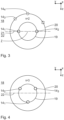
- Fig. 3 shows another possible arrangement of X-ray source regions 14; in the arrangement plane 18. Shown are two X-ray source regions 14 1 , 14 2 which both are arranged on an inner arrangement circle 19, such inner arrangement circle 19 being defined by a center Z. These two X-ray source regions 14 1 , 14 2 define a same polar chief ray angle, but define different azimuthal chief ray angles with respect to the object plane 17. A y-distance between the X-ray source regions 14 1 , 14 2 in the fig. 3 embodiment may be equal to the y-separation between the X-ray source regions 14 2 and 14 4 in the fig. 2 embodiment.
- X-ray source regions 14 3 , ... may be arranged, in particular along a line 21 parallel to the y-direction defined by the two X-ray source regions 14 1 , 14 2 or as indicated with dashed circles on such outer arrangement circle 20, at different circle positions (different azimuthal angles) not coinciding with such line 21.
- Distances between X-ray source regions 14; exhibiting the same polar chief ray angle may be attributed to detectors 7 i having the same distance to such X-ray source region 14 i .
- n source spots on a single circle helps to increase the throughput by a factor of n, since instead of a full rotation (360°) of the sample only the fraction 360°/n is needed to reach the same number of projections.
- those detection areas or detectors being assigned to the respective source spot also can be arranged on a single circle. If source spots are arranged on different circles, this can help to increase image quality, since different polar angles can be used for the reconstruction.
- both the radii of the source spots 14; as well as the positions of the detector 7 i might be changed in order to cover a broader angular spectrum.
- Fig. 4 shows in a view similar to fig. 3 an arrangement of three X-ray source regions 14 1 , 14 2 , 14 3 which, in this case, are equidistantly arranged on the inner arrangement circle 19. With respect to a vertical xy-plane 2, these three X-ray source regions 14 1 to 14 3 in fig. 4 all are arranged out of plane. This contrasts to the fig. 3 arrangement, where the X-ray source regions 14 1 , 14 2 are arranged in plane.
- a particular arrangement of the source spots 14 may follow from a requirement to evenly distribute n spots on a respective circle. Dependent on the respective embodiment, an absolute orientation within a coordinate system may not be relevant.
- FIG. 5 Another arrangement embodiment of the X-ray source regions 14; is shown in fig. 5 , here in the exemplified case of four X-ray source regions 14 1 to 14 4 .
- all of the X-ray source regions 14 1 to 14 4 are arranged equidistantly on the inner arrangement circle 19.
- Fig. 6 shows a further embodiment with another variant of an arrangement of X-ray source regions 14;.
- nine X-ray source regions 14 1 to 14 9 are depicted with solid lines.
- a first X-ray source region 14 1 is located in a center of the concentric inner and outer arrangement circles 19, 20.
- Such central X-ray source region 14 1 has the same coordinates in y- and in z-direction as a center of the region of interest 10.
- This central X-ray source region 14 1 also may be omitted.
- Four further X-ray source regions 14 2 to 14 5 are arranged similar to the X-ray source region arrangement of fig. 5 equidistantly on the inner arrangement circle 19.
- X-ray source regions 14 6 to 14 9 also are arranged equidistantly, but now on a first outer arrangement circle 20.
- X-ray source regions 14 6 , 14 2 ,14 1 , 14 4 , 14 8 are arranged in line on a line parallel to the z-axis.
- X-ray source regions 14 9 , 14 5 , 14 1 , 14 3 and 14 7 are arranged in line on a line parallel to the y-axis.
- Such in-line y-arrangement is similar to that shown in fig. 2 .
- further X-ray source regions 14 10 , ... may be arranged on a further outer arrangement circle 23 which also is concentric to the arrangement circles 19 and 20 and has the largest radius.
- Such further X-ray source regions 14 i are shown with broken lines in fig. 6 .
- These further X-ray source regions may be also positioned in an in-line configuration (same azimuthal angles, different polar angles) as exemplified by X-ray source regions 14 10 , 14 12 , and 14 13 , but also may be arranged off-line (different azimuthal angles, same or different polar angles), as shown with X-ray source region and 14n.
- such further X-ray source regions 14 10 , ... could be all arranged in an in-line configuration.
- the X-ray source regions 14 2 to 14s on the one hand and 14 6 to 14 9 on the other are arranged at the same polar angles, respectively, on the respective arrangement circles 19 and 20.
- X-ray source region 14 i arrangements of various further kinds also are conceivable. With such further configurations, all X-ray source regions 14 i may be located on an own circle, i.e. no pair of X-ray source regions 14 i , 14 j is located on the same arrangement circle.
- Fig. 7 shows a further embodiment of an X-ray source 24 which may be used in the X-ray inspection system 1 instead of the X-ray source 9.
- Components and functions which already were discussed with respect to figs 1 to 6 above show the same reference numerals and are not discussed in detail again.
- an embodiment of an X-ray source is possible, wherein such X-ray source consists of n electron beam emitters and each beam gets split into m beamlets thus yielding a total of n x m beamlets.
- the X-ray source 24 has a single electron beam source 25 to generate a main electron beam 26 and a subsequent electron beam splitting unit 27 to split the main electron beam 26 into a plurality of separate partial electron beams 13 1 , 13 2 , 13 3 .
- the separate partial electron beams 13 are accelerated via respective acceleration units 28 1 , 28 2 , and 28 3 .
- the accelerated electron beams 13 are further conditioned regarding their direction towards the arrangement plane 18 and regarding their focal position with a focusing and beam steering unit 29.
- Such unit 29 in fig. 7 is depicted as a single unit and is schematically shown as a single lens.
- each of the accelerated partial electron beams 13 may have its own, separate focusing and beam steering unit 29 i .
- the beam steering unit 29 may include several separate sub-units arranged along a respective beam path of the electron beams 13 i .
- the multi aperture lenslet array 35 is driven to be positioned more closely to the arrangement plane 18 resulting in an arrangement of the X-ray source regions 14; which are, as compared to fig. 8 , more distant to each other.
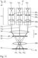
- Figs 10 and 11 show another embodiment of an X-ray source 37 which may be used in the X-ray inspection system 1 instead of the X-ray source 30.
- Components and functions which already were discussed with respect to figs 1 to 7 above show the same reference numerals and are not discussed in detail again.
- the X-ray source 37 has a plurality of electron beam sources 12 1 , 12 2 and 12 3 with attributed acceleration units 28; serving to accelerate a respective one of the separate electron beams 13; generated by the electron beam sources 12;.
- the acceleration unit 28 together with the electron beam sources 12 i and a further electron beam focusing unit (schematically depicted lenses 28a), the acceleration unit 28; constitute a multi e-beam column 11 comparable to that of the embodiment of fig. 2 .
- Figs 10 and 11 exemplify two focusing and beam steering positions of the focusing and beam steering unit 29 of the X-ray source 37.
- the multi aperture lenslet array 35 is omitted and the function of such lenslet array is taken over by another lens 28b which schematically is depicted in fig. 11 .
- another lens 28b which schematically is depicted in fig. 11 .
- such lens 28b may be omitted.
Landscapes
- Health & Medical Sciences (AREA)
- Immunology (AREA)
- Chemical & Material Sciences (AREA)
- Analytical Chemistry (AREA)
- Biochemistry (AREA)
- General Health & Medical Sciences (AREA)
- Life Sciences & Earth Sciences (AREA)
- General Physics & Mathematics (AREA)
- Pathology (AREA)
- Physics & Mathematics (AREA)
- Toxicology (AREA)
- Engineering & Computer Science (AREA)
- Pulmonology (AREA)
- Radiology & Medical Imaging (AREA)
- Theoretical Computer Science (AREA)
- Nuclear Medicine, Radiotherapy & Molecular Imaging (AREA)
- Analysing Materials By The Use Of Radiation (AREA)
Abstract
An X-ray inspection system (1) serves for inspection of an object (2). An X-ray source (9) of the system serves for generating X-rays to propagate through a region of interest (ROI, 10) of the object (2). An object mount holds the object (2) to be inspected such that the ROI (10) is accessible for the generated X-rays. A detection system (7a) serves to detect the X-rays after propagation through the ROI (10). The X-ray source (9) generates a plurality of separate X-ray light bundles (9i) to propagate through the ROI (10). Chief rays (16i) of at least two of the generated separate X-ray light bundles (9i) impinge on the ROI (10) of the object (2) with different chief ray illumination angles (CRAi). The detection system (7a) comprises separate detection areas to detect the separate X-ray light bundles (9i), respectively. An inspection system results enabling an inspection of an object with fast image data acquisition.
Description
- The contents of PCT patent application
PCT/EP 2023/080 855 - The invention refers to an X-ray inspection system for inspection of an object.
- 3D imaging of a sample structure by acquiring a set of 2D images of differently oriented sample planes is known in particular with respect to 3D X-ray imaging. In that respect, it is referred to Kasperl S., Hiller J., Krumm M., Computed tomography metrology in industrial research and development, Materials Testing, June 1, 2009;51(6):405-11 and to Körner, L., Lawes, S., Senin, N., Leach, R., Simulation of continuous high aspect ratio tomography for surface topography measurements, paper shown in DXCT 2019, Huddersfield. Further, respective projection systems and acquisition methods are known from Welkenhuyzen, F., Kiekens, K., Pierlet, M., Dewulf, W., Bleys, P. & Kruth, J.-P. and Voet, A., Industrial computer tomography for dimensional metrology: Overview of influence factors and improvement strategies, OPTIMESS 2009 or from Hsieh J., Computed tomography principles, design, artifacts, and recent advances, SPIE press, 2003.
WO 2008/002132 A1 discloses a method and an apparatus for imaging. Further imaging optical arrangements to image an object illuminated by X-rays are known fromUS 7,057,187 B1 , fromUS 7,130,375 B1 and fromUS 9,129,715 B2 DE 10 2018 209 570 A1 a method and a device to produce a three-dimensional image is known.US 2022/0178851 A1 discloses a high throughput 3D X-ray laminography imaging system using a transmission X-ray source.US 2011/0249795 A1 discloses an X-ray inspection method and an X-ray inspection apparatus.US 2015/110252 A1 discloses X-ray sources using linear accumulation.US 2022/0328277 A1 discloses a method and a device for producing and using multiple origins of X-radiation.US 2004/0240616 A1 discloses devices and methods for producing multiple X-ray beams from multiple locations. - It is an object of the present invention to enable an inspection of an object which as compared to 3D X-ray imaging devices of the prior art results in a faster image data acquisition.
- This object is met by an X-ray inspection system having the features of
claim 1. - According to the invention, a region of interest of the object to be inspected is illuminated simultaneously with X-ray light bundles impinging on the ROI with different chief illumination angles. As a result, with one and the same relative orientation and arrangement of the X-ray source to the object, a respective plurality of differently oriented sample planes may be imaged leading in effect to the possibility of a "one shot" 3D X-ray imaging of the object. The simultaneous illumination with X-ray bundles impinging on the ROI with different chief ray illumination angles can lead to a substantial increase in X-ray throughput.
- A chief ray of a respective X-ray light bundle is a central ray within such X-ray light bundle. Such central ray, i.e. the chief ray, may impinge centrally on the respective detection area. The chief ray may impinge perpendicular on the respective detection area.
- The number of differently generated X-ray light bundles may be in a range between 2 and 20, in particular between 2 and 10. In particular, the X-ray source may generate 2, 3, 4, 5 or more separate X-ray light bundles impinging on the ROI of the object with different chief illumination angles. In general, such number of generated separate X-ray light bundles impinging on the ROI of the object with different chief illumination angles may be smaller than 50.
- Objects to be inspected may have several layers of interconnects and may include absorbing structures such as redistribution layers (RDLs) or metal pads.
- Objects to be inspected may be multi-chip modules. In particular, whole wafers or printed circuit boards, i.e. objects having lateral dimensions of more than 100 mm and in particular up to 300 or 500 mm may be inspected.
- The X-ray inspection system may be embodied as an X-ray laminography inspection system. The object mount of such X-ray inspection system may be embodied corresponding to a sample motion stage disclosed in
US 2022/0178851 A1 . The object mount may include in particular a rotary stage to rotate the object around an axis which in particular is perpendicular to an object surface. - Alternatively or in addition, the object mount may be embodied to pivot or rotate the object around another pivot or rotation axis.
- Via the simultaneous illumination with X-ray light bundles impinging on the ROI with different chief ray illumination angles simultaneously different perspectives of one and the same ROI may be recorded during operation of the X-ray inspection system. In case the X-ray inspection system is embodied as an X-ray laminography imaging system, instead of a full 360° rotation of the object to obtain full inspection information, a half rotation (180°) of the object may be sufficient. Merging the information in particular obtained from two opposing chief ray illumination angles then delivers the full 360° image and in particular may deliver a full 3D image of the object. If more than two X-ray light bundles are used, in particular, if n X-ray light bundles are used, the rotation angle can be reduced to 360°/n.
- An X-ray source according to
claim 2 having separate electron beam sources leads to a high flexibility of the X-ray source. Each of the separate electron beams may be controlled independently. Each of the electron beam sources may have an own attributed electron beam acceleration unit. - The converting element may be a tungsten element.
- An X-ray source according to
claim 3 only needs a single electron beam source diminishing in that respect a complexity of the X-ray source. Each split partial electron beam may be equipped with its own acceleration unit. Alternatively, a common acceleration unit may be provided for all split partial electron beams. - With an X-ray source according to
claim 4, the initially generated main electron beam is accelerated by an acceleration unit. With such an embodiment, different acceleration units provided for the split partial electron beams may be omitted. Alternatively, again each split partial electron beam may have its own acceleration unit. - An arrangement of the X-ray source regions according to
claim 5 facilitates a subsequent guiding of the respectively generated X-ray light bundles to propagate through a region of interest. - An arrangement according to
claim 6 may be beneficial with respect to space requirements of the X-ray source components. A center of such arrangement circles may define an illumination angle "0°". The X-ray source regions may be arranged on several circles having different circle radii. - An arrangement according to
claim 7 has been proven to be of specific usability. Alternatively or in addition, at least some or all of the X-ray source regions may be arranged at different azimuthal angles on the respective circles. - An electron beam optics according to
claim 8 increases a flexibility of a usability of the X-ray source. Different and in particular controllable chief illumination angles via which the separate X-ray light bundles impinge on the ROI of the object may be provided. - An aperture device according to
claim 9 avoids an undesired crosstalk between the respective beam paths. - A plurality of detection devices according to
claim 10 improves a flexibility of the X-ray detection of the inspection system. - This, in particular, holds true for an embodiment according to
claim 11. The sensor array may be a CCD or a CMOS array. - The detection system may include a post-magnification unit. In particular, an optical system may be used to image a magnified image via visible photons which are emitted from a scintillator on which the X-rays impinge after propagation through the ROI. Possible embodiments for such a post-magnification detection are known from
US 9,129,715 B2 - Chief ray illumination angles of the respective X-ray light bundles on the one hand and distances between the respective X-ray source regions and the detectors respectively attributed to these light bundles on the other may be chosen such that a geometrical magnification at all detectors of the detection system, in particular at all separate detection areas to detect the respective X-ray light bundle, is the same. In particular, in case all X-ray light bundles are emitted from sources which are arranged in a plane being parallel to an object plane, all detection areas or detectors being attributed to the respective X-ray light bundles being emitted from such X-ray sources also may be arranged in a plane parallel to such object plane. In particular, all detection areas, preferably all detectors may be arranged in exactly one plane.
- In addition to chief rays of at least two of the generated separate X-ray light bundles which impinge on the ROI of the object with different polar chief ray illumination angles, chief rays of at least two of the generated separate X-ray light bundles may impinge on the ROI of the object with different azimuthal chief ray illumination angles.
- As long as the separate X-ray light bundles impinge on the ROI of the object with equal polar chief ray illumination angles, the distance between a respective X-ray source region and an attributed detector may also be equal.
- The separate detection areas or the separate detectors may be tilted such that the respectively attributed X-ray light bundle impinges on such detection area or detector with normal incidence. Alternatively, an incidence angle between a chief ray of the respective X-ray light bundle and the attributed detection area or detector may deviate from 0°. Such angle of incidence may be in a range between 0° and 60°, in particular in a range between 0° and 45° or in a range between 0° and 30°. Such incidence angle may be in a range between 0° and 7°.
- In particular, it is possible to image object structures which are smaller than 20 µm, smaller than 10 µm and in particular which are smaller than 1 µm. Examples for such structures are Cu-Cu hybrid bonding structures between microchips and substrate conductor paths. In particular, direct bonds between single dies or between a whole wafer onto a substrate wafer can be inspected.
- In particular, a 3D tomographic reconstruction of an object sample under investigation by combining several 2D images taken from different directions is possible.
- X-ray energies of the used X-rays can range between 5 keV and 160 keV, preferably between 15 keV and 90 keV.
- With the inspection system, in particular complex 3D IC semiconductor packages may be inspected.
- Exemplified embodiments of the invention hereinafter are described with reference to the accompanying drawings. It is shown in
- Fig. 1
- a schematic working principle of an X-ray inspection system for inspection of an object, embodied as a projection system for acquiring 3D tomographic images of semiconductor structure samples via acquiring a set of 2D images of differently oriented sample planes with a respective acquisition method;
- Fig. 2
- in a sectional view according to the xy-plane in
fig. 1 an embodiment of the X-ray inspection system having an X-ray source being embodied with a multi e-beam column, wherein the X-ray source comprises five X-ray source spots to generate five separate X-ray light bundles to impinge on a region of interest (ROI) of the object; - Fig. 3
- in a yz-view an example of a distribution of source spots of another embodiment of an X-ray source of the X-ray inspection system according to
fig. 2 ; - Fig. 4
- in a view similar to
fig. 3 another possible distribution of source spots of a respective embodiment of the X-ray source; - Fig. 5
- in a view similar to
fig. 3 another possible distribution of source spots of a respective embodiment of the X-ray source; - Fig. 6
- in a view similar to
fig. 3 another possible distribution of source spots of a respective embodiment of the X-ray source; - Fig. 7
- an embodiment of the X-ray source of the X-ray inspection system having a single e-beam emitter and having several separate e-beam acceleration units to generate separate X-ray light bundles to propagate through the ROI of the object in a side view;
- Fig. 8
- in a view similar to
fig. 7 another embodiment of an X-ray source having a single emitter multi e-beam source to generate a plurality of separate X-ray light bundles; - Fig. 9
- the embodiment of
fig. 8 with another position of a multi aperture lenslet array to alter a location of e-beam foci of different e-beams generated by the source; - Fig. 10
- in a view similar to
figs 7 to 9 , another embodiment of an X-ray source generating a plurality of separate X-ray light bundles, the X-ray source having an array of multiple, separate single e-beam sources; - Fig. 11
- in a view similar to
fig. 10 , another X-ray source having an array of multiple, separate single beam sources with another beam optics to alter a location of beam foci of the generated electron beams. -
Fig. 1 shows schematically main components of an X-ray inspection system embodied as aprojection system 1 for acquiring tomographic images of a sample orobject 2 by acquiring a set of two-dimensional (2D) images of differently oriented sample planes. - The
sample 2 in the shown embodiment is a semiconductor structure. - The
projection system 1 comprises aprojection light source 3. Theprojection light source 3 is embodied as an X-ray source. - The
sample 2 is held by asample structure holder 4 which as an illustration of prior art is shown to be rotatable around at least onesample rotating axis 5. According to the invention described here, differently oriented sample planes which are required for 3D image acquirement, are produced different to a sample rotation as explained with respect tofigs 2 et seq below. - To facilitate the description of the structures and their orientation, in the following a Cartesian xyz coordinate system is used. In
fig. 1 , the x-axis runs to the right. The y-axis runs perpendicular to the drawing plane offig. 1 away from the viewer. The z-axis runs upwards infig. 1 . - The
sample rotating axis 5 runs parallel to the z-axis. - The
sample structure holder 4 holds thesample 2 in alight path 6 of the projection light generated by theprojection light source 3. - In the
light path 6 after the sample 2 a spatially resolvingdetector 7 is arranged which is embodied as a CCD or a CMOS detector. Thedetector 7 may include an optical post-magnification. A respective detector with optical post-magnification is known fromUS 9,129,715 B2 - A detection plane of the
detector 7 is parallel to the yz-plane. Therotation axis 5 of thesample holder 4 runs parallel to such detection plane. Suchsample structure holder 4 also is referred to as an object mount. - Between the
sample 2 and thedetector 7 and in the vicinity of thedetector 7, ascintillator layer 8 is arranged in thelight path 6. Thescintillator layer 8 serves to convert a wavelength of the projection light into a wavelength detectable by thedetector 7, in particular into a UV and/or visible wavelength. - The
detector 7 together with the scintillator layer and possible further detection components is referred to herein after also as adetection system 7a. -
Fig. 2 shows an embodiment of anX-ray source 9 to generate a plurality of separateX-ray light bundles 91 to 95 to propagate through a region of interest (ROI) 10 of theobject 2. - The
X-ray source 9 comprises a multi electron-beam (e-beam)column 11 having a plurality of separate electron beam sources 121 to 12 5 to generate respectively separate electron beams 131 to135. Further, theX-ray light source 9 includes a converting element attributed to the separate electron beam sources 13; to convert the generated electron beams 13; to separate X-source spots or regions 141 to 14s. The converting element may be embodied as a respective tungsten layer on an X-ray source body located at the respective X-ray source region 14i. The tungsten layer may include tungsten regions being embedded in a diamond substrate layer. Such diamond substrate layer provides an excellent heat conduction to dissipate a thermal load induced by the electron beams 13;. The converting element may be embodied as a continuous plate carrying respective tungsten layers at least at the position of the X-ray source regions 14i. - The
X-ray light bundles 9; separately generated in the X-ray source regions 14; are defined with respect to their outer beam boundaries to propagate from the respective X-ray source region 14; through the region ofinterest 10 of theobject 2. Such propagation definition is given by anaperture device 15 arranged in the beam path of the respective X-raylight bundle 9; between the X-ray source regions 14; and theobject 2. Theaperture device 15 is embodied as an aperture blade having aperture through-holes 151 to 155 for the passage of the respective X-raylight bundle 91 to 95. - The
detection system 7a of thefig. 2 embodiment of theX-ray inspection system 1 comprises a plurality of spatially resolvingdetectors 71 to 7s. Each of thosedetectors 7i may be embodied as described above with respect tofig. 1 . Therespective detection device 7i defines a detection area to detect the respective X-raylight bundle 9i. Thedetectors 7i may be embodied as optically coupled detectors. A conversion of the X-ray wavelength to optical wavelengths may take place. - The
detectors 71 to 7s are located in the beam path of the respectiveX-ray light bundles 91 to 95 after their passage through theROI 10 of theobject 2. - Chief rays 161 to 165 of the separate
X-ray light bundles 91 to 95 impinge on theROI 10 of theobject 2 with different chief ray illumination angles CRAi. In particular, these chief rays 161 to 165 exhibit different polar chief ray illumination angles CRAi with respect to an object plane. The chief ray illumination angles CRA1 and CRA5 each are approximately 15°. An angle difference between chief ray angles CRAi and CRAi+1 is for i = 1 to 4 37,5° each. - As an alternative to such equispaced arrangements of the chief ray angles CRAi, also a non-equispaced arrangement is possible. Chief ray angles CRAi on the one hand, and distances between the respective X-ray source region 14; and the attributed
detector 7i on the other may be in an alternative arrangement chosen such that a geometrical magnification at alldetectors 7i is the same. Such geometrical magnification is determined by a projected width of theROI 10 as seen by theX-ray light bundle 9; having a respective polar chief ray illumination angle CRAi. Such projected width, for example, is largest for detector 73 (CRA3 = 90°) requiring to enable an equalized geometrical magnification a relatively small distance between thedetector 73 and the X-ray source region 143, and is smallest seen fromdetectors 71 and 75 (CRA1 = CRA5 = 15°) requiring a distance between the X-ray source regions 141, 14s, and thedetectors detector 73 distance, larger. In other words, to cover a comparable surface area on thedetectors 7i being the result of a respective impingement of theROI 10 via theX-ray light bundles 9i having different chief ray illumination angles CRAi, thosedetectors 7i assigned to X-raylight bundles 9i with small chief ray angles CRAi have a larger distance to theROI 10 and also to the respective X-ray source region 14i as compared to X-raylight bundles 9; having a larger chief ray illumination angle CRAi. The more tilted theROI 10 is seen by the respective X-raylight bundle 9i, the more distant the assigneddetector 7i should be arranged to achieve the same geometrical magnification of theROI 10. - The chief ray 163 impinges on the region of
interest 10 of theobject 2 with normal incidence to theobject plane 17 which runs parallel to the yz-plane. - The five different columns of the multi e-beam column (i = 1 to 5) 11 each have an electron acceleration unit not shown in detail in
Fig. 2 . - Such acceleration unit may be embodied as a common electron acceleration unit for all of such columns of the
multi e-beam column 11. Alternatively, each column (i = 1 to 5) may have its own electron acceleration unit within themulti e-beam column 11. - In the
fig. 2 embodiment, the X-ray source regions 14; are arranged in anarrangement plane 18 which runs parallel to objectplane 17. In particular, the X-ray source regions 14; may be arranged along a line withinsuch arrangement plane 18. Such line may be parallel to the y-direction. - The
arrangement plane 18 also is referred to as source plane and defines a source plane of the respective X-ray source of the X-ray inspection system embodiment. - The
detectors 7i may be arranged in the vertical plane according tofigure 2 in a half circle. - In a different configuration as shown in
figure 2 , alldetectors 7i may be arranged in exactly one plane. Such arrangement plane may be parallel to theobject plane 17. -
Fig. 3 shows another possible arrangement of X-ray source regions 14; in thearrangement plane 18. Shown are two X-ray source regions 141, 142 which both are arranged on aninner arrangement circle 19, suchinner arrangement circle 19 being defined by a center Z. These two X-ray source regions 141, 142 define a same polar chief ray angle, but define different azimuthal chief ray angles with respect to theobject plane 17. A y-distance between the X-ray source regions 141, 142 in thefig. 3 embodiment may be equal to the y-separation between the X-ray source regions 142 and 144 in thefig. 2 embodiment. Further, on anouter arrangement circle 20 defining another polar chief ray angle, further X-ray source regions 143, ... may be arranged, in particular along a line 21 parallel to the y-direction defined by the two X-ray source regions 141, 142 or as indicated with dashed circles on suchouter arrangement circle 20, at different circle positions (different azimuthal angles) not coinciding with such line 21. Distances between X-ray source regions 14; exhibiting the same polar chief ray angle may be attributed todetectors 7i having the same distance to such X-ray source region 14i. - The arrangement of n source spots on a single circle helps to increase the throughput by a factor of n, since instead of a full rotation (360°) of the sample only the fraction 360°/n is needed to reach the same number of projections. If several source spots are arranged on a single circle, those detection areas or detectors being assigned to the respective source spot also can be arranged on a single circle. If source spots are arranged on different circles, this can help to increase image quality, since different polar angles can be used for the reconstruction. During a scan, both the radii of the source spots 14; as well as the positions of the
detector 7i might be changed in order to cover a broader angular spectrum. -
Fig. 4 shows in a view similar tofig. 3 an arrangement of three X-ray source regions 141, 142, 143 which, in this case, are equidistantly arranged on theinner arrangement circle 19. With respect to a vertical xy-plane 2, these three X-ray source regions 141 to 143 infig. 4 all are arranged out of plane. This contrasts to thefig. 3 arrangement, where the X-ray source regions 141, 142 are arranged in plane. A particular arrangement of the source spots 14; may follow from a requirement to evenly distribute n spots on a respective circle. Dependent on the respective embodiment, an absolute orientation within a coordinate system may not be relevant. - Another arrangement embodiment of the X-ray source regions 14; is shown in
fig. 5 , here in the exemplified case of four X-ray source regions 141 to 144. Here, all of the X-ray source regions 141 to 144 are arranged equidistantly on theinner arrangement circle 19. -
Fig. 6 shows a further embodiment with another variant of an arrangement of X-ray source regions 14;. In thefig. 6 embodiment, nine X-ray source regions 141 to 149 are depicted with solid lines. A first X-ray source region 141 is located in a center of the concentric inner and outer arrangement circles 19, 20. Such central X-ray source region 141 has the same coordinates in y- and in z-direction as a center of the region ofinterest 10. This central X-ray source region 141 also may be omitted. Four further X-ray source regions 142 to 145 are arranged similar to the X-ray source region arrangement offig. 5 equidistantly on theinner arrangement circle 19. - Four further X-ray source regions 146 to 149 also are arranged equidistantly, but now on a first
outer arrangement circle 20. X-ray source regions 146, 142,141, 144, 148 are arranged in line on a line parallel to the z-axis. X-ray source regions 149, 145, 141, 143 and 147 are arranged in line on a line parallel to the y-axis. Such in-line y-arrangement is similar to that shown infig. 2 . - In addition, further X-ray source regions 1410, ... may be arranged on a further
outer arrangement circle 23 which also is concentric to the arrangement circles 19 and 20 and has the largest radius. Such further X-ray source regions 14i are shown with broken lines infig. 6 . These further X-ray source regions may be also positioned in an in-line configuration (same azimuthal angles, different polar angles) as exemplified by X-ray source regions 1410, 1412, and 1413, but also may be arranged off-line (different azimuthal angles, same or different polar angles), as shown with X-ray source region and 14n. In particular, such further X-ray source regions 1410, ... could be all arranged in an in-line configuration. - The X-ray source regions 142 to 14s on the one hand and 146 to 149 on the other are arranged at the same polar angles, respectively, on the respective arrangement circles 19 and 20.
- X-ray source region 14i arrangements of various further kinds also are conceivable. With such further configurations, all X-ray source regions 14i may be located on an own circle, i.e. no pair of X-ray source regions 14i, 14j is located on the same arrangement circle.
-
Fig. 7 shows a further embodiment of an X-ray source 24 which may be used in theX-ray inspection system 1 instead of theX-ray source 9. Components and functions which already were discussed with respect tofigs 1 to 6 above show the same reference numerals and are not discussed in detail again. Further, an embodiment of an X-ray source is possible, wherein such X-ray source consists of n electron beam emitters and each beam gets split into m beamlets thus yielding a total of n x m beamlets. - The X-ray source 24 has a single
electron beam source 25 to generate amain electron beam 26 and a subsequent electronbeam splitting unit 27 to split themain electron beam 26 into a plurality of separate partial electron beams 131, 132, 133. Subsequently to the electronbeam splitting unit 27, the separate partial electron beams 13; are accelerated via respective acceleration units 281, 282, and 283. Subsequently, the accelerated electron beams 13; are further conditioned regarding their direction towards thearrangement plane 18 and regarding their focal position with a focusing andbeam steering unit 29.Such unit 29 infig. 7 is depicted as a single unit and is schematically shown as a single lens. Alternatively, each of the accelerated partial electron beams 13; may have its own, separate focusing andbeam steering unit 29i. Further, thebeam steering unit 29 may include several separate sub-units arranged along a respective beam path of the electron beams 13i. - With the focusing and
beam steering unit 29, positions of the respective X-ray source regions 14; at thearrangement plane 18 can be adjusted and controlled. Using a respective number of separate electron beams 13; split via a respective embodiment of the electronbeam splitting unit 27, a corresponding number of X-ray source regions 14; can be generated, in particular in one of the source region arrangements discussed above with respect tofigs 2 to 6 . - At the
arrangement plane 18, the electrons of the electron beams 13; again are converted to X-rays using a respectively attributed converting element, in particular made of tungsten. -
Fig. 8 shows a further embodiment of anX-ray source 30 which may be used in theX-ray inspection system 1 instead of the X-ray source 24. Components and functions which already were discussed with respect tofigs 1 to 7 above show the same reference numerals and are not discussed in detail again. - In the
X-ray source 30, functions of an electronbeam splitting unit 27 and of an acceleration unit 28 are combined within a single emittermulti beam source 31. Such single emittermulti beam source 31 comprises the singleelectron beam source 25 and further comprises a multiaperture lenslet array 32 which serves to accelerate the electrons generated by theelectron source 25 and which further has a plurality of aperture openings 331 to 335 for the passage of in this way generated separate partial electron beams 13i. - The multi
aperture lenslet array 32 serves in particular as an acceleration unit to accelerate and to split themain electron beam 26 into the separate partial electron beams 131 to 135. - The multi
aperture lenslet array 32 may be part of an electron beam optics to focus and/or to steer directions of separate paths of the respective electron beams 13;. - A
macro lens 34 and a further multiaperture lenslet array 35 in a subsequent beam path of the separate partial electron beams 13; serve to condition propagation directions and/or focusing points of the respective separate partial electron beam 13; comparable to the focusing andbeam steering unit 29 of the X-ray source 24 offig. 7 . - Via a
drive unit 36, the multiaperture lenslet array 35 can be moved along a x-direction, i.e. perpendicular to thearrangement plane 18. -
Figs 8 and 9 show two different x-positions of the multiaperture lenslet array 35. In the x-position of the multiaperture lenslet array 35 shown infig. 8 ,such array 35 has a larger distance to thearrangement plane 18 as compared tofig. 9 . - In the
fig. 8 position of the multiaperture lenslet array 35, this results in an arrangement of the X-ray source region 141 to 14s which have a closer distance to each other. - In the
fig. 9 x-position, the multiaperture lenslet array 35 is driven to be positioned more closely to thearrangement plane 18 resulting in an arrangement of the X-ray source regions 14; which are, as compared tofig. 8 , more distant to each other. - Again, with the focusing and
beam steering unit 29 of theX-ray source 30 comprising themacro lens 34 and the multiaperture lenslet array 35, arrangements of the X-ray source regions 14; are possible, dependent on the number of generated separate partial electron beams 14i, which are discussed above with respect, in particular, tofigs 2 to 7 . -
Figs 10 and11 show another embodiment of anX-ray source 37 which may be used in theX-ray inspection system 1 instead of theX-ray source 30. Components and functions which already were discussed with respect tofigs 1 to 7 above show the same reference numerals and are not discussed in detail again. - The
X-ray source 37 has a plurality of electron beam sources 121, 122 and 123 with attributed acceleration units 28; serving to accelerate a respective one of the separate electron beams 13; generated by the electron beam sources 12;. Together with the electron beam sources 12i and a further electron beam focusing unit (schematically depictedlenses 28a), the acceleration unit 28; constitute amulti e-beam column 11 comparable to that of the embodiment offig. 2 . - Each of the acceleration units 28; comprises a single aperture lenslet.
- In the beam path subsequent to the
multi e-beam column 11 of theX-ray source 37, again, a focusing andbeam steering unit 29 comparable to that of the embodiment offigs 8 and 9 is arranged comprising amacro lens 34 and a driven multiaperture lenslet array 35. -
Figs 10 and11 exemplify two focusing and beam steering positions of the focusing andbeam steering unit 29 of theX-ray source 37. - In the position of
fig. 10 , closely spaced X-ray source regions 141, 142, and 143 result comparable to the spacing shown in the five beam embodiment offig. 8 . - In the further focusing and beam steering position of the focusing and
beam steering unit 29 shown infig. 11 with the multiaperture lenslet array 35 translated along the x-direction, the respective separate electron beams 13; cross each other in a beam crossing region 38. - In a further embodiment based on the
fig. 11 x-ray source 37, the multiaperture lenslet array 35 is omitted and the function of such lenslet array is taken over by anotherlens 28b which schematically is depicted infig. 11 . In the embodiment of thex-ray source 37 having the multiaperture lenslet array 35,such lens 28b may be omitted. - Regarding focusing and beam steering means, concepts may be used which are known from
WO 2008/002132 A1 .
Claims (12)
- An X-ray inspection system (1) for inspection of an object (2), the inspection system (1) comprising:- an X-ray source (9; 24; 30; 37) for generating X-rays to propagate through a region of interest (ROI, 10) of the object (2),- an object mount (4) to hold the object (2) to be inspected such that the ROI (10) is accessible for the generated X-rays,- a detection system (7a) to detect the X-rays after propagation through the ROI (10),- wherein the X-ray source (9; 24; 30; 37) generates a plurality of separate X-ray light bundles (9i) to propagate through the ROI (10),- wherein chief rays (16i) of at least two of the generated separate X-ray light bundles (9i) impinge on the ROI (10) of the object (2) with different chief ray illumination angles (CRAi),- wherein the detection system (7a) comprises separate detection areas to detect the separate X-ray light bundles (9i), respectively,- wherein the X-ray inspection system is embodied such that the ROI (10) of the object (2) to be inspected is illuminated simultaneously with X-ray light bundles (9i) impinging on the ROI (10) with different chief illumination angles (CRAi).
- The X-ray inspection system according to claim 1, wherein the X-ray source (9; 37) comprises a plurality of separate electron beam sources (12i) with an attributed converting element to convert the generated electron beams at separate X-ray source regions (14i) into X-rays.
- The X-ray inspection system according to claim 1, wherein the X-ray source (24; 30) comprises a single electron beam source (25) to generate a main electron beam (26), an electron beam splitting unit (27; 32) to split the main electron beam (26) into a plurality of separate partial electron beams (13i) and an attributed converting element to convert the generated partial electron beams at separate X-ray source regions (14i) into X-rays.
- The X-ray inspection system according to claim 1, wherein the X-ray source (30) comprises- a single electron beam source (25) to generate a main electron beam (26)- an acceleration unit (32) to accelerate and to split the main electron beam (26) into a plurality of separate partial electron beams (13i) and- an attributed converting element to convert the generated partial electron beams (13i) at separate X-ray source regions (14i) into X-rays.
- The X-ray inspection system according to one of claims 2 to 4 wherein the X-ray source regions (14i) are arranged in a source plane (18) of the inspection system (1).
- The X-ray inspection system according to claim 5, wherein several X-ray source regions (14i) are arranged on at least one circle (19; 19, 20; 19, 20, 23) in the source plane (18).
- The X-ray inspection system according to claim 6, wherein several X-ray source regions (14i) are arranged on several circles (19, 20; 19, 20, 23) in the source plane (18) with different radii and the X-ray source regions (14i) on different circles (19, 20; 19, 20, 23) are arranged at same polar angles on the respective circle (19, 20; 19, 20, 23).
- The X-ray inspection system according to one of claims 2 to 7, comprising an electron beam optics (29; 34, 35; 32, 34, 35) in an electron beam path of the electron beams (13i) upwards the X-ray source regions (14i) to focus and/or to steer a direction of the separate paths of the respective electron beams (13i).
- The X-ray inspection system according to one of claims 1 to 8, comprising an aperture device (15) arranged in a beam path between the X-ray source region (14i) and the region of interest (10).
- The X-ray inspection system according to one of claims 1 to 9, wherein the detection system (7a) comprises a plurality of detection devices (7i) and each of the detection devices (7i) is attributed to a separate X-ray light bundle (9i).
- The X-ray inspection system according to claim 10, wherein each of the detection devices (7i) comprises a sensor array.
- The X-ray inspection system according to one of claims 1 to 11, wherein the detection system (7a) includes a post-magnification unit.
Applications Claiming Priority (1)
| Application Number | Priority Date | Filing Date | Title |
|---|---|---|---|
| PCT/EP2023/080855 WO2025098589A1 (en) | 2023-11-06 | 2023-11-06 | X-ray inspection system for inspection of an object |
Publications (1)
| Publication Number | Publication Date |
|---|---|
| EP4549919A1 true EP4549919A1 (en) | 2025-05-07 |
Family
ID=88745761
Family Applications (1)
| Application Number | Title | Priority Date | Filing Date |
|---|---|---|---|
| EP24208471.3A Pending EP4549919A1 (en) | 2023-11-06 | 2024-10-23 | X-ray inspection system for inspection of an object |
Country Status (5)
| Country | Link |
|---|---|
| US (1) | US20250146958A1 (en) |
| EP (1) | EP4549919A1 (en) |
| KR (1) | KR20250066436A (en) |
| TW (1) | TW202536404A (en) |
| WO (1) | WO2025098589A1 (en) |
Families Citing this family (1)
| Publication number | Priority date | Publication date | Assignee | Title |
|---|---|---|---|---|
| KR102916716B1 (en) * | 2025-07-15 | 2026-01-23 | 주식회사 덕인 | X-ray tube, X-ray generator and X-ray imaging system |
Citations (12)
| Publication number | Priority date | Publication date | Assignee | Title |
|---|---|---|---|---|
| US20040240616A1 (en) | 2003-05-30 | 2004-12-02 | Applied Nanotechnologies, Inc. | Devices and methods for producing multiple X-ray beams from multiple locations |
| US7057187B1 (en) | 2003-11-07 | 2006-06-06 | Xradia, Inc. | Scintillator optical system and method of manufacture |
| US7130375B1 (en) | 2004-01-14 | 2006-10-31 | Xradia, Inc. | High resolution direct-projection type x-ray microtomography system using synchrotron or laboratory-based x-ray source |
| WO2008002132A1 (en) | 2006-06-27 | 2008-01-03 | Technische Universiteit Delft | Method and apparatus for imaging |
| US20110249795A1 (en) | 2008-12-22 | 2011-10-13 | Omron Corporation | X-ray inspection method and x-ray inspection apparatus |
| WO2014047518A1 (en) * | 2012-09-20 | 2014-03-27 | Virginia Tech Intellectual Properties, Inc. | Stationary source computed tomography and ct-mri systems |
| US20150110252A1 (en) | 2013-09-19 | 2015-04-23 | Wenbing Yun | X-ray sources using linear accumulation |
| US9129715B2 (en) | 2012-09-05 | 2015-09-08 | SVXR, Inc. | High speed x-ray inspection microscope |
| EP2940456A1 (en) * | 2012-12-31 | 2015-11-04 | Nuctech Company Limited | Article inspection device using distributed x-ray source |
| DE102018209570A1 (en) | 2017-06-14 | 2018-12-20 | Carl Zeiss Industrielle Messtechnik Gmbh | Method and device for generating a three-dimensional image |
| US20220178851A1 (en) | 2020-12-07 | 2022-06-09 | Sigray, Inc. | High throughput 3d x-ray imaging system using a transmission x-ray source |
| US20220328277A1 (en) | 2020-07-06 | 2022-10-13 | Michael Keith Fuller | Method and device for producing and using multiple origins of x-radiation |
-
2023
- 2023-11-06 WO PCT/EP2023/080855 patent/WO2025098589A1/en active Pending
-
2024
- 2024-10-23 EP EP24208471.3A patent/EP4549919A1/en active Pending
- 2024-10-31 US US18/933,281 patent/US20250146958A1/en active Pending
- 2024-11-05 KR KR1020240155067A patent/KR20250066436A/en active Pending
- 2024-11-06 TW TW113142572A patent/TW202536404A/en unknown
Patent Citations (13)
| Publication number | Priority date | Publication date | Assignee | Title |
|---|---|---|---|---|
| CN1833299A (en) * | 2003-05-30 | 2006-09-13 | 新泰科有限公司 | Devices and methods for producing multiple x-ray beams from multiple locations |
| US20040240616A1 (en) | 2003-05-30 | 2004-12-02 | Applied Nanotechnologies, Inc. | Devices and methods for producing multiple X-ray beams from multiple locations |
| US7057187B1 (en) | 2003-11-07 | 2006-06-06 | Xradia, Inc. | Scintillator optical system and method of manufacture |
| US7130375B1 (en) | 2004-01-14 | 2006-10-31 | Xradia, Inc. | High resolution direct-projection type x-ray microtomography system using synchrotron or laboratory-based x-ray source |
| WO2008002132A1 (en) | 2006-06-27 | 2008-01-03 | Technische Universiteit Delft | Method and apparatus for imaging |
| US20110249795A1 (en) | 2008-12-22 | 2011-10-13 | Omron Corporation | X-ray inspection method and x-ray inspection apparatus |
| US9129715B2 (en) | 2012-09-05 | 2015-09-08 | SVXR, Inc. | High speed x-ray inspection microscope |
| WO2014047518A1 (en) * | 2012-09-20 | 2014-03-27 | Virginia Tech Intellectual Properties, Inc. | Stationary source computed tomography and ct-mri systems |
| EP2940456A1 (en) * | 2012-12-31 | 2015-11-04 | Nuctech Company Limited | Article inspection device using distributed x-ray source |
| US20150110252A1 (en) | 2013-09-19 | 2015-04-23 | Wenbing Yun | X-ray sources using linear accumulation |
| DE102018209570A1 (en) | 2017-06-14 | 2018-12-20 | Carl Zeiss Industrielle Messtechnik Gmbh | Method and device for generating a three-dimensional image |
| US20220328277A1 (en) | 2020-07-06 | 2022-10-13 | Michael Keith Fuller | Method and device for producing and using multiple origins of x-radiation |
| US20220178851A1 (en) | 2020-12-07 | 2022-06-09 | Sigray, Inc. | High throughput 3d x-ray imaging system using a transmission x-ray source |
Non-Patent Citations (4)
| Title |
|---|
| HSIEH J.: "Computed tomography principles, design, artifacts, and recent advances", 2003, SPIE PRESS |
| KASPERL S.HILLER J.KRUMM M.: "Computed tomography metrology in industrial research and development", MATERIALS TESTING, vol. 51, no. 6, 1 June 2009 (2009-06-01), pages 405 - 11 |
| TO KÖRNER, L.LAWES, S.SENIN, N.LEACH, R.: "Simulation of continuous high aspect ratio tomography for surface topography measurements, paper shown", DXCT, 2019 |
| WEL-KENHUYZEN, F.KIEKENS, K.PIERLET, M.DEWULF, W.BLEYS, P.KRUTH, J.-P.VOET, A.: "Industrial computer tomography for dimensional metrology: Overview of influence factors and improvement strategies", OPTIMESS, 2009 |
Also Published As
| Publication number | Publication date |
|---|---|
| KR20250066436A (en) | 2025-05-13 |
| TW202536404A (en) | 2025-09-16 |
| US20250146958A1 (en) | 2025-05-08 |
| WO2025098589A1 (en) | 2025-05-15 |
Similar Documents
| Publication | Publication Date | Title |
|---|---|---|
| US7130375B1 (en) | High resolution direct-projection type x-ray microtomography system using synchrotron or laboratory-based x-ray source | |
| US10692184B2 (en) | Super-resolution X-ray imaging method and apparatus | |
| TW573118B (en) | Off-center tomosynthesis | |
| US7215736B1 (en) | X-ray micro-tomography system optimized for high resolution, throughput, image quality | |
| US5787146A (en) | X-ray imaging system using diffractive x-ray optics for high definition low dosage three dimensional imaging of soft tissue | |
| WO2010029862A1 (en) | X-ray inspection device and method for x-ray inspection | |
| US20150055745A1 (en) | Phase Contrast Imaging Using Patterned Illumination/Detector and Phase Mask | |
| JP4587668B2 (en) | Spot grating array electron imaging system | |
| KR20230105675A (en) | Method and Apparatus for Detecting Defects in Semiconductor Systems | |
| US9726624B2 (en) | Using multiple sources/detectors for high-throughput X-ray topography measurement | |
| JP2009515152A (en) | Equipment for X-ray tomographic synthesis | |
| US10352881B2 (en) | Computed tomography | |
| US20250146958A1 (en) | X-ray inspection system for inspection of an object | |
| KR20180008577A (en) | Defect determination method, and X-ray inspection apparatus | |
| JP7442375B2 (en) | Multi-electron beam inspection device and multi-electron beam inspection method | |
| JP5177236B2 (en) | X-ray inspection method and X-ray inspection apparatus | |
| US11992350B2 (en) | System and method for compact laminography utilizing microfocus transmission x-ray source and variable magnification x-ray detector | |
| GB2399730A (en) | X ray inspection system | |
| CN117795624A (en) | Imaging optical configuration for imaging objects illuminated by X-rays | |
| KR102679097B1 (en) | Oblique ct device for semiconductor inspection with adjustable field of view | |
| JP7385493B2 (en) | Multi-charged particle beam alignment method and multi-charged particle beam inspection device | |
| US10504683B2 (en) | Device and method for forming a plurality of charged particle beamlets | |
| US11461939B2 (en) | Tomographic method of determining a 3D map of a charge collection efficiency and an apparatus for performing the method | |
| JP2009036575A (en) | X-ray inspection apparatus and X-ray inspection method | |
| JP3107593B2 (en) | Pattern inspection equipment |
Legal Events
| Date | Code | Title | Description |
|---|---|---|---|
| PUAI | Public reference made under article 153(3) epc to a published international application that has entered the european phase |
Free format text: ORIGINAL CODE: 0009012 |
|
| STAA | Information on the status of an ep patent application or granted ep patent |
Free format text: STATUS: THE APPLICATION HAS BEEN PUBLISHED |
|
| AK | Designated contracting states |
Kind code of ref document: A1 Designated state(s): AL AT BE BG CH CY CZ DE DK EE ES FI FR GB GR HR HU IE IS IT LI LT LU LV MC ME MK MT NL NO PL PT RO RS SE SI SK SM TR |
|
| STAA | Information on the status of an ep patent application or granted ep patent |
Free format text: STATUS: REQUEST FOR EXAMINATION WAS MADE |
|
| 17P | Request for examination filed |
Effective date: 20251015 |