EP4549371A1 - Microfluidic device - Google Patents
Microfluidic device Download PDFInfo
- Publication number
- EP4549371A1 EP4549371A1 EP23831133.6A EP23831133A EP4549371A1 EP 4549371 A1 EP4549371 A1 EP 4549371A1 EP 23831133 A EP23831133 A EP 23831133A EP 4549371 A1 EP4549371 A1 EP 4549371A1
- Authority
- EP
- European Patent Office
- Prior art keywords
- chip
- joint
- main
- substrate
- microfluidic device
- Prior art date
- Legal status (The legal status is an assumption and is not a legal conclusion. Google has not performed a legal analysis and makes no representation as to the accuracy of the status listed.)
- Pending
Links
Images




Classifications
-
- B—PERFORMING OPERATIONS; TRANSPORTING
- B01—PHYSICAL OR CHEMICAL PROCESSES OR APPARATUS IN GENERAL
- B01L—CHEMICAL OR PHYSICAL LABORATORY APPARATUS FOR GENERAL USE
- B01L3/00—Containers or dishes for laboratory use, e.g. laboratory glassware; Droppers
- B01L3/50—Containers for the purpose of retaining a material to be analysed, e.g. test tubes
- B01L3/502—Containers for the purpose of retaining a material to be analysed, e.g. test tubes with fluid transport, e.g. in multi-compartment structures
- B01L3/5027—Containers for the purpose of retaining a material to be analysed, e.g. test tubes with fluid transport, e.g. in multi-compartment structures by integrated microfluidic structures, i.e. dimensions of channels and chambers are such that surface tension forces are important, e.g. lab-on-a-chip
- B01L3/50273—Containers for the purpose of retaining a material to be analysed, e.g. test tubes with fluid transport, e.g. in multi-compartment structures by integrated microfluidic structures, i.e. dimensions of channels and chambers are such that surface tension forces are important, e.g. lab-on-a-chip characterised by the means or forces applied to move the fluids
-
- B—PERFORMING OPERATIONS; TRANSPORTING
- B01—PHYSICAL OR CHEMICAL PROCESSES OR APPARATUS IN GENERAL
- B01L—CHEMICAL OR PHYSICAL LABORATORY APPARATUS FOR GENERAL USE
- B01L3/00—Containers or dishes for laboratory use, e.g. laboratory glassware; Droppers
- B01L3/50—Containers for the purpose of retaining a material to be analysed, e.g. test tubes
- B01L3/502—Containers for the purpose of retaining a material to be analysed, e.g. test tubes with fluid transport, e.g. in multi-compartment structures
- B01L3/5027—Containers for the purpose of retaining a material to be analysed, e.g. test tubes with fluid transport, e.g. in multi-compartment structures by integrated microfluidic structures, i.e. dimensions of channels and chambers are such that surface tension forces are important, e.g. lab-on-a-chip
- B01L3/502707—Containers for the purpose of retaining a material to be analysed, e.g. test tubes with fluid transport, e.g. in multi-compartment structures by integrated microfluidic structures, i.e. dimensions of channels and chambers are such that surface tension forces are important, e.g. lab-on-a-chip characterised by the manufacture of the container or its components
-
- B—PERFORMING OPERATIONS; TRANSPORTING
- B01—PHYSICAL OR CHEMICAL PROCESSES OR APPARATUS IN GENERAL
- B01J—CHEMICAL OR PHYSICAL PROCESSES, e.g. CATALYSIS OR COLLOID CHEMISTRY; THEIR RELEVANT APPARATUS
- B01J19/00—Chemical, physical or physico-chemical processes in general; Their relevant apparatus
- B01J19/0093—Microreactors, e.g. miniaturised or microfabricated reactors
-
- B—PERFORMING OPERATIONS; TRANSPORTING
- B01—PHYSICAL OR CHEMICAL PROCESSES OR APPARATUS IN GENERAL
- B01L—CHEMICAL OR PHYSICAL LABORATORY APPARATUS FOR GENERAL USE
- B01L3/00—Containers or dishes for laboratory use, e.g. laboratory glassware; Droppers
- B01L3/50—Containers for the purpose of retaining a material to be analysed, e.g. test tubes
- B01L3/502—Containers for the purpose of retaining a material to be analysed, e.g. test tubes with fluid transport, e.g. in multi-compartment structures
- B01L3/5027—Containers for the purpose of retaining a material to be analysed, e.g. test tubes with fluid transport, e.g. in multi-compartment structures by integrated microfluidic structures, i.e. dimensions of channels and chambers are such that surface tension forces are important, e.g. lab-on-a-chip
- B01L3/502715—Containers for the purpose of retaining a material to be analysed, e.g. test tubes with fluid transport, e.g. in multi-compartment structures by integrated microfluidic structures, i.e. dimensions of channels and chambers are such that surface tension forces are important, e.g. lab-on-a-chip characterised by interfacing components, e.g. fluidic, electrical, optical or mechanical interfaces
-
- B—PERFORMING OPERATIONS; TRANSPORTING
- B01—PHYSICAL OR CHEMICAL PROCESSES OR APPARATUS IN GENERAL
- B01L—CHEMICAL OR PHYSICAL LABORATORY APPARATUS FOR GENERAL USE
- B01L9/00—Supporting devices; Holding devices
- B01L9/52—Supports specially adapted for flat sample carriers, e.g. for plates, slides, chips
- B01L9/527—Supports specially adapted for flat sample carriers, e.g. for plates, slides, chips for microfluidic devices, e.g. used for lab-on-a-chip
-
- B—PERFORMING OPERATIONS; TRANSPORTING
- B81—MICROSTRUCTURAL TECHNOLOGY
- B81B—MICROSTRUCTURAL DEVICES OR SYSTEMS, e.g. MICROMECHANICAL DEVICES
- B81B1/00—Devices without movable or flexible elements, e.g. microcapillary devices
- B81B1/002—Holes characterised by their shape, in either longitudinal or sectional plane
-
- G—PHYSICS
- G01—MEASURING; TESTING
- G01N—INVESTIGATING OR ANALYSING MATERIALS BY DETERMINING THEIR CHEMICAL OR PHYSICAL PROPERTIES
- G01N15/00—Investigating characteristics of particles; Investigating permeability, pore-volume or surface-area of porous materials
- G01N15/10—Investigating individual particles
- G01N15/14—Optical investigation techniques, e.g. flow cytometry
- G01N15/1484—Optical investigation techniques, e.g. flow cytometry microstructural devices
-
- B—PERFORMING OPERATIONS; TRANSPORTING
- B01—PHYSICAL OR CHEMICAL PROCESSES OR APPARATUS IN GENERAL
- B01J—CHEMICAL OR PHYSICAL PROCESSES, e.g. CATALYSIS OR COLLOID CHEMISTRY; THEIR RELEVANT APPARATUS
- B01J2219/00—Chemical, physical or physico-chemical processes in general; Their relevant apparatus
- B01J2219/00781—Aspects relating to microreactors
- B01J2219/00801—Means to assemble
- B01J2219/00804—Plurality of plates
-
- B—PERFORMING OPERATIONS; TRANSPORTING
- B01—PHYSICAL OR CHEMICAL PROCESSES OR APPARATUS IN GENERAL
- B01J—CHEMICAL OR PHYSICAL PROCESSES, e.g. CATALYSIS OR COLLOID CHEMISTRY; THEIR RELEVANT APPARATUS
- B01J2219/00—Chemical, physical or physico-chemical processes in general; Their relevant apparatus
- B01J2219/00781—Aspects relating to microreactors
- B01J2219/00801—Means to assemble
- B01J2219/00804—Plurality of plates
- B01J2219/00806—Frames
-
- B—PERFORMING OPERATIONS; TRANSPORTING
- B01—PHYSICAL OR CHEMICAL PROCESSES OR APPARATUS IN GENERAL
- B01J—CHEMICAL OR PHYSICAL PROCESSES, e.g. CATALYSIS OR COLLOID CHEMISTRY; THEIR RELEVANT APPARATUS
- B01J2219/00—Chemical, physical or physico-chemical processes in general; Their relevant apparatus
- B01J2219/00781—Aspects relating to microreactors
- B01J2219/00801—Means to assemble
- B01J2219/00804—Plurality of plates
- B01J2219/00808—Sealing means
-
- B—PERFORMING OPERATIONS; TRANSPORTING
- B01—PHYSICAL OR CHEMICAL PROCESSES OR APPARATUS IN GENERAL
- B01J—CHEMICAL OR PHYSICAL PROCESSES, e.g. CATALYSIS OR COLLOID CHEMISTRY; THEIR RELEVANT APPARATUS
- B01J2219/00—Chemical, physical or physico-chemical processes in general; Their relevant apparatus
- B01J2219/00781—Aspects relating to microreactors
- B01J2219/00801—Means to assemble
- B01J2219/0081—Plurality of modules
- B01J2219/00813—Fluidic connections
-
- B—PERFORMING OPERATIONS; TRANSPORTING
- B01—PHYSICAL OR CHEMICAL PROCESSES OR APPARATUS IN GENERAL
- B01J—CHEMICAL OR PHYSICAL PROCESSES, e.g. CATALYSIS OR COLLOID CHEMISTRY; THEIR RELEVANT APPARATUS
- B01J2219/00—Chemical, physical or physico-chemical processes in general; Their relevant apparatus
- B01J2219/00781—Aspects relating to microreactors
- B01J2219/00851—Additional features
- B01J2219/00867—Microreactors placed in series, on the same or on different supports
-
- B—PERFORMING OPERATIONS; TRANSPORTING
- B01—PHYSICAL OR CHEMICAL PROCESSES OR APPARATUS IN GENERAL
- B01J—CHEMICAL OR PHYSICAL PROCESSES, e.g. CATALYSIS OR COLLOID CHEMISTRY; THEIR RELEVANT APPARATUS
- B01J2219/00—Chemical, physical or physico-chemical processes in general; Their relevant apparatus
- B01J2219/00781—Aspects relating to microreactors
- B01J2219/00851—Additional features
- B01J2219/00871—Modular assembly
-
- B—PERFORMING OPERATIONS; TRANSPORTING
- B01—PHYSICAL OR CHEMICAL PROCESSES OR APPARATUS IN GENERAL
- B01J—CHEMICAL OR PHYSICAL PROCESSES, e.g. CATALYSIS OR COLLOID CHEMISTRY; THEIR RELEVANT APPARATUS
- B01J2219/00—Chemical, physical or physico-chemical processes in general; Their relevant apparatus
- B01J2219/00781—Aspects relating to microreactors
- B01J2219/00891—Feeding or evacuation
-
- B—PERFORMING OPERATIONS; TRANSPORTING
- B01—PHYSICAL OR CHEMICAL PROCESSES OR APPARATUS IN GENERAL
- B01L—CHEMICAL OR PHYSICAL LABORATORY APPARATUS FOR GENERAL USE
- B01L2200/00—Solutions for specific problems relating to chemical or physical laboratory apparatus
- B01L2200/02—Adapting objects or devices to another
- B01L2200/025—Align devices or objects to ensure defined positions relative to each other
-
- B—PERFORMING OPERATIONS; TRANSPORTING
- B01—PHYSICAL OR CHEMICAL PROCESSES OR APPARATUS IN GENERAL
- B01L—CHEMICAL OR PHYSICAL LABORATORY APPARATUS FOR GENERAL USE
- B01L2200/00—Solutions for specific problems relating to chemical or physical laboratory apparatus
- B01L2200/02—Adapting objects or devices to another
- B01L2200/026—Fluid interfacing between devices or objects, e.g. connectors, inlet details
- B01L2200/027—Fluid interfacing between devices or objects, e.g. connectors, inlet details for microfluidic devices
-
- B—PERFORMING OPERATIONS; TRANSPORTING
- B01—PHYSICAL OR CHEMICAL PROCESSES OR APPARATUS IN GENERAL
- B01L—CHEMICAL OR PHYSICAL LABORATORY APPARATUS FOR GENERAL USE
- B01L2200/00—Solutions for specific problems relating to chemical or physical laboratory apparatus
- B01L2200/02—Adapting objects or devices to another
- B01L2200/028—Modular arrangements
-
- B—PERFORMING OPERATIONS; TRANSPORTING
- B01—PHYSICAL OR CHEMICAL PROCESSES OR APPARATUS IN GENERAL
- B01L—CHEMICAL OR PHYSICAL LABORATORY APPARATUS FOR GENERAL USE
- B01L2200/00—Solutions for specific problems relating to chemical or physical laboratory apparatus
- B01L2200/06—Fluid handling related problems
- B01L2200/0689—Sealing
-
- B—PERFORMING OPERATIONS; TRANSPORTING
- B01—PHYSICAL OR CHEMICAL PROCESSES OR APPARATUS IN GENERAL
- B01L—CHEMICAL OR PHYSICAL LABORATORY APPARATUS FOR GENERAL USE
- B01L2300/00—Additional constructional details
- B01L2300/08—Geometry, shape and general structure
- B01L2300/0809—Geometry, shape and general structure rectangular shaped
- B01L2300/0816—Cards, e.g. flat sample carriers usually with flow in two horizontal directions
-
- B—PERFORMING OPERATIONS; TRANSPORTING
- B01—PHYSICAL OR CHEMICAL PROCESSES OR APPARATUS IN GENERAL
- B01L—CHEMICAL OR PHYSICAL LABORATORY APPARATUS FOR GENERAL USE
- B01L2300/00—Additional constructional details
- B01L2300/08—Geometry, shape and general structure
- B01L2300/0861—Configuration of multiple channels and/or chambers in a single devices
- B01L2300/087—Multiple sequential chambers
-
- B—PERFORMING OPERATIONS; TRANSPORTING
- B01—PHYSICAL OR CHEMICAL PROCESSES OR APPARATUS IN GENERAL
- B01L—CHEMICAL OR PHYSICAL LABORATORY APPARATUS FOR GENERAL USE
- B01L2300/00—Additional constructional details
- B01L2300/08—Geometry, shape and general structure
- B01L2300/0861—Configuration of multiple channels and/or chambers in a single devices
- B01L2300/0874—Three dimensional network
-
- B—PERFORMING OPERATIONS; TRANSPORTING
- B01—PHYSICAL OR CHEMICAL PROCESSES OR APPARATUS IN GENERAL
- B01L—CHEMICAL OR PHYSICAL LABORATORY APPARATUS FOR GENERAL USE
- B01L2300/00—Additional constructional details
- B01L2300/08—Geometry, shape and general structure
- B01L2300/0887—Laminated structure
-
- B—PERFORMING OPERATIONS; TRANSPORTING
- B01—PHYSICAL OR CHEMICAL PROCESSES OR APPARATUS IN GENERAL
- B01L—CHEMICAL OR PHYSICAL LABORATORY APPARATUS FOR GENERAL USE
- B01L2400/00—Moving or stopping fluids
- B01L2400/08—Regulating or influencing the flow resistance
- B01L2400/084—Passive control of flow resistance
- B01L2400/086—Passive control of flow resistance using baffles or other fixed flow obstructions
Definitions
- the disclosure relates to a microfluidic device.
- a microfluidic device is a general term for devices in which minute spaces such as microchannels and reaction vessels are created in a plate-shaped microfluidic chip by a microfabrication technology. Since processing such as separation, stirring, heat treatment, fluorescence detection can be subjected to liquids such as a culture solution, a reagent through the use of minute spaces, the microfluidic device has been used for research in a wide range of fields including biotechnology, life sciences, medicine, and chemical engineering.
- a microfluidic device which handles a liquid within a minute space has been attracting attention as a technology that can reduce the used amount of precious sample. Since plural processing such as liquid separation, stirring, heat treatment, and fluorescence detection can be performed within the same device, they also contribute to shortening of a reaction time.
- microfluidic device is used in a wide range of fields and supports a wide variety of research activities.
- microfluidic device is manufactured from materials such as acrylic, glass, and silicone rubber. No matter which material is selected, its manufacturing takes a lot of time and cost.
- Patent Documents 1 to 3 there has been proposed a method of appropriately combining a plurality of microfluidic chips to create a desired microfluidic device.
- Patent Document 1 Japanese Patent Application Laid-Open No. 2005-147940
- Patent Document 2 discloses that a plurality of types of modules having different functions, which are provided with microchannels respectively, are prepared, and these modules are combined as appropriate to manufacture a microfluidic device corresponding to the purpose of use.
- Patent Document 3 A proposal in International Publication No. 2019/092989 (Patent Document 3) is to stack a plurality of plates for microfluidic chips with different flow channels to manufacture a microfluidic device fit for its intended use.
- the microfluidic device described in Japanese Patent Application Laid-Open Nos. 2005-147940 (Patent Document 1) and 2015-123012 (Patent Document 2) is described as a microfluidic device configured by attaching a microfluidic chip or a module to a holder (base member (2) in Patent Document 1 and holder (9) in Patent Document 2)). Therefore, the scale of the microfluidic device depends on the size of the holder, and it is not possible to realize a device which exceeds the size of the holder. Improvements are desired to allow more flexible expansion of a microfluidic device.
- the microfluidic device described in International Publication No. 2019/092989 has a structure in which the plates of the microfluidic chips are stacked, so that the microfluidic chips can be expanded without increasing the size of each plate.
- Patent Document 3 since it is not possible to expose the minute spaces such as the flow channel and the pressure vessel provided in the microfluidic chip located in the lower layer to the outside, it is not possible to observe and detect the liquid as the sample, or add desired processing thereto. It is not suitable for research that require observation of each sample or the like.
- a microfluidic device includes a plate-shaped main chip having a minute space inside into which a liquid is introduced, a plate-shaped joint chip having a communication flow path inside and having on both end sides of an upper surface thereof, a pair of joint communication holes for communicating the communication flow path to the minute space, and a guide.
- the guide has an upper holding area which holds the main chip, and a lower holding area which selectively holds one of both ends of the joint chip while being partially stacked on the main chip held in the upper holding area.
- the main chip includes a pair of main communication holes on both end sides of a lower surface of the main chip, the pair of main communication holes communicating the minute space with the joint communication hole of the joint chip held in the lower holding area while being held in the upper holding area.
- a microfluidic device 101 is configured with a plurality of microfluidic chips 11 connected in a row.
- Each individual microfluidic chip 11 mainly has a main chip 31 which is internally provided with a minute space MS such as a microchannel or a reaction vessel, and has a structure in which the main chip 31 is held together with a joint chip 51 by a guide 71 (refer to FIGS. 2 and 12 ).
- An X direction in FIG. 1 is the direction of arrangement of the microfluidic chips 11 and defines the length direction of each element.
- "Both ends” and “ends” of the microfluidic device 101, microfluidic chip 11, main chip 31, joint chip 51, and guide 71 mean both ends and ends in the X direction, respectively.
- a Y direction in FIG. 1 is the direction perpendicular to the direction of arrangement of the microfluidic chips 11 and defines the width direction of each element.
- "Both side ends” and “side parts” of the microfluidic device 101, microfluidic chip 11, main chip 31, joint chip 51, and guide 71 mean both side ends and side parts in the Y direction, respectively.
- a Z direction in FIG. 1 defines the vertical direction of the microfluidic device 101, microfluidic chip 11, main chip 31, joint chip 51, and guide 71.
- the top surface appears above as viewed in the Z direction in FIG. 1
- the bottom surface appears below as viewed in the Z direction in FIG. 1 .
- the main chip 31 has the same length (length in the X direction) as the guide 71, and is held by the guide 71 without protruding therefrom. Therefore, when the individual microfluidic chips 11 are arranged in a row and connected, the main chips 31 and guides 71 included in the two adjacent microfluidic chips 11 are in contact with each other at both end surfaces thereof.
- the mutually contacting end surfaces of the two adjacent microfluidic guides 71 are referred to as mounting surfaces 72 (refer to FIG. 11 ).
- the joint chip 51 is arranged in a stack on the two adjacent main chips 31 so as to straddle them.
- the area to hold the main chip 31 is an upper holding area 73
- the area to hold the joint chip 51 is a lower holding area 74 (refer to FIG. 11 ).
- a flow channel FC including the minute space MS is formed.
- the following elements form the flow channel FC.
- the supply hole 32 is essential from the perspective of the entire structure of the microfluidic device 101, but when viewed on the individual microfluidic chip 11 basis, the supply hole 32 is not essential for all microfluidic chips 11. Therefore, the main chips 31 include a type provided with the supply hole 32 and a type without the supply hole 32, which are mixed together.
- the two main chips 31 on the front side are of a type having supply holes 32
- the two main chips 31 on the back side are of a type without supply holes 32.
- the main chip 31 provided with the supply holes 32 will be described as an example, but all main chips 31 are not provided with the supply holes 32.
- the main chip 31 of type with no supply holes 32 please note that the supply holes 32 are eliminated from the main chip 31 introduced below.
- the main chip 31 is a rectangular-shaped plate-like substrate, and is configured by stacking three acrylic plates each having translucency. They are three of a middle layer main substrate 34, an upper layer main substrate 35, and a lower layer main substrate 36.
- the main chip 31 is manufactured by positioning the upper layer main substrate 35 on an upper surface of the middle layer main substrate 34 and the lower layer main substrate 36 on a lower surface thereof respectively and thermocompression-bonding them.
- All three acrylic plates (34, 35, and 36) use the same shape and size with a 20 mm square.
- the thickness of the middle layer main substrate 34 is 0.5 mm
- the thickness of the upper layer main substrate 35 is 1.0 mm
- the thickness of the lower layer main substrate 36 is 0.5 mm.
- the middle layer main substrate 34 is provided with an opening portion 37 which becomes a minute space MS.
- the shape of the minute space MS defined by the opening portion 37 can be determined as appropriate depending on the use of each individual microfluidic chip 11.
- the upper layer main substrate 35 is provided on both end sides with a pair of supply holes 32 communicating with the minute space MS.
- the lower layer main substrate 36 is provided on both end sides with a pair of main communication holes 33 communicating with the minute space MS.
- the main chip 31 which is completed by thermocompression-bonding the three stacked acrylic plates (34, 35, and 36), has a form in which the minute space MS can be visually recognized from the outside as illustrated in FIG. 1 .
- the main chip 31 of the type having no supply holes 32 can be manufactured in the same manner by using the plain upper layer main substrate 35 having no supply holes 32.
- the main chip 31 is a rectangular-shaped plate-like substrate, and is configured by stacking two acrylic plates each having translucency. They are two of a main substrate 34A and an upper layer main substrate 35.
- the main chip 31 is manufactured by positioning the upper layer main substrate 35 on an upper surface of the main substrate 34A and bonding it by thermocompression.
- Both of the two acrylic plates (34A and 35) forming the two layers use the same shape and size with a 20 mm square.
- the thickness of both the main substrate 34A and the upper layer main substrate 35 is 1.0 mm.
- the main substrate 34A is provided with a minute space MS and a pair of main communication holes 33.
- the shape of the minute space MS can be determined as appropriate depending on the use of each individual microfluidic chip 11.
- the pair of main communication holes 33 they are provided on both end sides of the main chip 31 so as to communicate with the lower surface of the main substrate 34A.
- the upper layer main substrate 35 is provided with a pair of supply holes 32 on both end sides thereof, which communicates with the minute space MS.
- the main chip 31 which is completed by thermocompression-bonding the two stacked acrylic plates (34A and 35), has a form in which the minute space MS can be visually recognized from the outside as illustrated in FIG. 1 .
- the main chip 31 of the type having no supply holes 32 can be manufactured in the same manner by using the plain upper layer main substrate 35 having no supply holes 32.
- a plurality of types of standardized main chips 31 having various types of minute spaces MS each having a typical shape of a flow path or a reaction vessel may be prepared in advance so that an appropriate selection can be made.
- the main chip 31 having the supply holes 32 and the main chip 31 having no supply holes 32 can also be similarly standardized.
- a main chip 31 (dedicated part) having such a minute space MS is manufactured each time.
- the middle layer main substrate 34 and the lower layer main substrate 36 in the first aspect conceptually correspond to the main substrate 34A in the second aspect.
- the two acrylic plates (34, 36) are stacked and bonded to generate the main substrate 34A (middle layer main substrate 34, lower layer main substrate 36), and in the second aspect, the single acrylic plate (34A) is used to generate the main substrate 34A (middle layer main substrate34, lower layer main substrate 36). Therefore, it can be said that the difference between the first aspect and the second aspect resides in the method of manufacturing the main substrate 34A.
- a 3D printer can be used to realize an integrally shaped product of the main substrate 34A and the upper layer main substrate 35.
- a support material is provided in advance in the portions which become the minute space MS, the supply hole 32, and the pair of main communication holes 33 to create modeling inclusive of the support material as well.
- a plate-shaped main chip 31 is completed which has the minute space MS thereinside and has the supply hole 32 communicating with the minute space MS on its upper surface, and which has the pair of main communication holes 33 on both end sides of its lower surface, which communicates with the minute space MS.
- the main chip 31 is made of one or more acrylic plates (34 to 36, 34A, and 35), that is, an acrylic resin, but the main chip 31 may be manufactured using as materials, such as polydimethylsiloxane (PDMS), glass, polycarbonate (PC), polyethylene terephthalate (PET), cycloolefin polymer (COP) without being limited to the acrylic resin.
- the main chip 31 can be manufactured using various types of materials such as an ABS resin, a PLA resin, an ASA resin (strong in weather resistance), a PP resin (strong in heat resistance and chemical resistance), a PC resin, a nylon resin, an acrylic resin, PETG, thermoplastic polyurethane.
- the joint chip 51 is a rectangular-shaped plate-like substrate, and is configured by stacking three acrylic plates each having translucency. They are three of a middle layer joint substrate 54, an upper layer joint substrate 55, and a lower layer joint substrate 56.
- the joint chip 51 is manufactured by positioning the upper layer joint substrate 55 on an upper surface of the middle layer joint substrate 54, and the lower layer joint substrate 56 on its lower surface and bonding them by thermocompression, respectively.
- the three acrylic plates (54, 55, and 56) forming the three layers all use the same shape and size with a 10 mm square. They all have the same thickness: the middle layer joint substrate 54 has a thickness of 0.5 mm, the upper layer joint substrate 55 has a thickness of 0.5 mm, and the lower layer joint substrate 56 also has a thickness of 0.5 mm.
- the middle layer joint substrate 54 is provided with an opening portion 57 which becomes a communication flow path 52.
- the upper layer joint substrate 55 is provided on both end sides with a pair of joint communication holes 53 communicating with the communication flow path 52.
- the lower layer joint substrate 56 is a plain acrylic plate with no holes or openings formed therein.
- a rubber sheet 58 is bonded to the upper surface of the joint chip 51 completed by thermocompression-bonding the three stacked acrylic plates (54, 55, and 56), i.e., the surface of the upper layer joint substrate 55.
- the bonding of the rubber sheet 58 to the surface of the upper layer joint substrate 55 is performed by, for example, adhesion.
- the rubber sheet 58 has the same size and shape as the three acrylic plates (54, 55, and 56) and is bonded thereto without being protruded or displaced from these acrylic plates (54, 55, and 56).
- the rubber sheet 58 is provided with a pair of through holes 58a in position alignment with these joint communication holes 53 so as not to block the pair of joint communication holes 53 provided on both end sides of the upper layer joint substrate 55.
- the joint chip 51 is a rectangular-shaped plate-like substrate, and is configured by stacking two acrylic plates each having translucency. They are two of a joint substrate 54A and an upper layer joint substrate 55.
- the joint chip 51 is manufactured by positioning the upper layer joint substrate 55 on an upper surface of the joint substrate 54A and bonding the same by thermocompression.
- the two acrylic plates (54A and 55) forming the two layers use the same shape and size, both of which are a 10 mm square.
- the joint substrate 54A is 1.0 mm in thickness
- the upper layer joint substrate 55 is 0.5 mm in thickness.
- the joint substrate 54A is provided with a communication flow path 52.
- the upper layer joint substrate 55 is provided on both end sides with a pair of joint communication holes 53 communicating with the communication flow path 52.
- a rubber sheet 58 is bonded to the upper surface of the joint chip 51 completed by thermocompression-bonding the two stacked acrylic plates (54A and 55), i.e., the surface of the upper layer joint substrate 55.
- the bonding of the rubber sheet 58 to the surface of the upper layer joint substrate 55 is performed by, for example, adhesion.
- the rubber sheet 58 has the same size and shape as the two acrylic plates (54A and 55) and is bonded thereto without being protruded or displaced from these acrylic plates (54A and 55).
- the rubber sheet 58 is provided with a pair of through holes 58a in position alignment with the pair of joint communication holes 53 so as not to block these joint communication holes 53 provided on both end sides of the upper layer joint substrate 55.
- the middle layer joint substrate 54 and the lower layer joint substrate 56 in the first aspect conceptually correspond to the joint substrate 54A in the second aspect.
- the two acrylic plates (54 and 56) are stacked and bonded to generate the joint substrate 54A (middle layer joint substrate 54, lower layer joint substrate 56), and in the second aspect, the single acrylic plate (54A) is used to generate the joint substrate 54A (middle layer joint substrate 54, lower layer joint substrate 56), respectively. Therefore, it can be said that the difference between the first aspect and the second aspect resides in the method of manufacturing the joint substrate 54A.
- the joint substrate 54A and the upper layer joint substrate 55 it is also possible to integrally shape the joint substrate 54A and the upper layer joint substrate 55.
- a 3D printer can be used to realize an integrally shaped product of the joint substrate 54A and the upper layer joint substrate 55.
- a support material is provided in advance in the portions which become the communication flow path 52 and the pair of joint communication holes 53 to create modeling inclusive of the support material as well.
- a plate-shaped joint chip 51 is completed which has the communication flow path 52 thereinside and has on both end sides of its upper surface, the pair of joint communication holes 53 for allowing the communication flow path 52 to communicate with the minute space MS.
- the joint chip 51 is made of one or more acrylic plates (54 to 56, 54A, and 55), that is, an acrylic resin, but the joint chip 51 may be manufactured using as materials, such as polydimethylsiloxane (PDMS), glass, polycarbonate (PC), polyethylene terephthalate (PET), cycloolefin polymer (COP) without being limited to the acrylic resin.
- the joint chip 51 can be manufactured using various types of materials such as an ABS resin, a PLA resin, an ASA resin (strong in weather resistance), a PP resin (strong in heat resistance and chemical resistance), a PC resin, a nylon resin, an acrylic resin, PETG, thermoplastic polyurethane.
- the guide 71 is shaped from, for example, a resin material, and includes the upper holding area 73 whose upper surface is made open, and the pair of lower holding areas 74 on both end sides of the upper holding area 73.
- the upper portions of both side walls of the upper holding area 73 overhang to face each other to thereby configure a pair of rails 75 which guides the sliding movement of the main chip 31.
- the main chip 31 is inserted from the mounting surface 72 along these rails 75 and is housed and held in the upper holding area 73.
- the main chip 31 housed in the upper holding area 73 exposes the minute space MS to the outside from the space between the pair of rails 75, thereby enabling visual recognition and processing operations from the outside.
- the pair of lower holding areas 74 are in communication with the mounting surface 72 in a form which is one step lower than the bottom surface of the upper holding area 73. Therefore, the lower holding area 74 opens toward the mounting surface 72 while the main chip 31 is held in the upper holding area 73 and receives mounting of the joint chip 51 by sliding movement.
- the depth of the lower holding area 74 is set to be half the length of the joint chip 51.
- the multiple microfluidic chips 11 can be connected in their length directions (X direction in FIG. 1 ).
- Connecting portions 76 provided in the mounting surface 72 of the guide 71 realizes such a connection between the microfluidic chips 11.
- the connecting portions 76 are configured by a plurality of magnets 76a embedded into the mounting surface 72.
- each individual guide 71 is given directionality.
- the surfaces to be joined facing each other are determined beforehand.
- the visible surface located on the front side in FIG. 11 is referred to as the mounting surface 72A
- the invisible surface on the deep side is referred to as the mounting surface 72B.
- the magnet 76a embedded in the mounting surface 72A is made different in polarity from the magnet 76a embedded in the mounting surface 72B.
- the magnets 76a attract each other with a magnetic force, and the two guides 71 can be connected in a fixed state.
- the guide 71 further has a restriction part 77 as well.
- the restriction part 77 has a structure which restricts the positional displacements of the two guides 71 in a stacking direction of the main chip 31 and the joint chip 51 when the two guides 71 are connected to each other.
- Such a restriction part 77 is configured by a convex step portion 77a provided on the mounting surface 72A and a concave step portion 77b provided on the mounting surface 72B.
- the convex step portion 77a protrudes from the mounting surface 72A in the length direction (X direction in FIG. 1 ).
- the concave step portion 77b retracts from the mounting surface 72B in the length direction so that they fit into each other.
- the convex step portion 77a of one guide 71 fits into the concave step portion 77b of another guide 71, or the concave step portion 77b of one guide 71 fits to the convex step portion 77a of another guide 71 to thereby restrict the positional displacements of the two guides 71 in the stacking direction of the main chip 31 and the joint chip 51.
- FIG. 12 is a perspective view of the microfluidic chip 11 according to the first embodiment using the main chip 31 and the joint chip 51 in the first embodiment
- FIG. 14 is a schematic view illustrating the microfluidic chip 11 according to the first embodiment with the guide 71 excluded.
- FIG. 13 is a perspective view of a microfluidic chip 11 according to a second embodiment using a main chip 31 and a joint chip 51 in the second embodiment
- FIG. 15 is a schematic view illustrating the microfluidic chip 11 according to the second embodiment with a guide 71 excluded.
- the microfluidic chip 11 is assembled by mounting the main chip 31 on the upper holding area 73 of the guide 71 and mounting the joint chip 51 on the lower holding area 74.
- the joint chip 51 is inserted and held in the lower holding area 74 by half its length, and the remaining half becomes in a state of protruding from the mounting surface 72.
- This protruding half of joint chip 51 is inserted and held in a lower holding area 74 provided in a guide 71 of another microfluidic chip 11 connected to the microfluidic chip 11.
- the main chip 31 and the joint chip 51 are stacked, and the respective minute spaces MS of the two microfluidic chips 11 are connected to the joint chip 51 to form a flow channel FC.
- a joint communication hole 53 provided in an upper layer joint substrate 55 of the joint chip 51 communicates with a main communication hole 33 provided in a lower layer main substrate 36 of the main chip 31.
- the respective minute spaces MS of the two microfluidic chips 11 are in communication via the main communication hole 33 of one microfluidic chip 11, the joint communication hole 53 on one end side of the joint chip 51 straddling the two microfluidic chips 11, the communication flow path 52, the joint communication hole 53 on the opposite end side thereof, and the main communication hole 33 of the other microfluidic chip 11.
- the gap between the stacked main chip 31 and joint chip 51 is sealed by a rubber sheet 58 provided on the upper surface of the joint chip 51 so that the liquid flowing through the flow channel FC is prevented from leaking.
- the seal structure which seals the flow channel FC between the main chip 31 and the joint chip 51 is not limited to the structure using the rubber sheet 58, but can also be achieved by a structure using an O-ring 61.
- the upper layer joint substrate 55 of the joint chip 51 is provided with an annular recess 62 so as to surround the circumferences of the pair of joint communication holes 53.
- the recess 62 forms a communication space CS in which the joint communication hole 53 and the main communication hole 33 connected to each other are located.
- the O-ring 61 is fitted into an inner wall 63 forming the recess 62 and slightly protrudes from the surface of the upper layer joint substrate 55, so that the O-ring 61 is brought into contact with the lower layer main substrate 36 (first embodiment) of the main chip 31 or the main substrate 34A thereof (second embodiment). Consequently, the O-ring 61 seals the communication space CS and prevents leakage of the liquid flowing through the flow channel FC at the connecting portion between the main chip 31 and the joint chip 51.
- the outer diameter of the O-ring 61 is larger than the inner diameter of the recess 62.
- the O-ring 61 fitted into the inner wall 63 of the recess 62 is in a state of being elastically deformed and bit into the recess 62.
- the microfluidic chip 11 is assembled.
- the joint chip 51 is inserted and held in the lower holding area 74 by half its length, and the remaining half becomes into a state of being protruded from the mounting surface 72.
- the protruded half of the joint chip 51 is inserted and held in the lower holding area 74 provided in the guide 71 of another microfluidic chip 11 connected to the microfluidic chip 11.
- the upper layer joint substrate 55 of the joint chip 51 protruding from the guide 71 exposes the O-ring 61 for connection with another main chip 31 held in the guide 71 of another microfluidic chip 11.
- the seal structure using the O-ring 61 is applicable even to both the microfluidic chip 11 in the first embodiment and the microfluidic chip 11 in the second embodiment.
- the combination of the microfluidic chips 11 each having the minute space MS suitable for the application is planned, and the microfluidic chips 11 are connected in one row to assemble the microfluidic device 101.
- a liquid such as a culture solution or a reagent is injected into the supply hole 32 prepared on the upper surface of the main chip 31 using an unillustrated pipe or syringe, and the like. Then, the liquid flows through the flow channel FC, and it becomes possible to perform processing such as liquid separation, stirring, heat treatment, fluorescence detection according to the selected minute space MS.
- the microfluidic device 101 according to the present embodiment has the following effects.
- the main chips 31 having the multiple types of minute spaces MS can be rearranged as desired, and the flow channel FC according to the purpose can be easily assembled. At this time, if the flow channel FC can be realized only by combining the main chips 31 each having the standardized minute space MS, the flow channel FC according to the purpose can be created on the spot without preparing special parts.
- main chips 31 are classified and prepared according to their functions, it is possible to easily perform operations such as surface treatment depending on the purpose of research.
- microfluidic chips 11 There is no limit to the number of the microfluidic chips 11 which can be connected, and excellent expandability can be obtained.
- the microfluidic chip 11 can be expanded simply by inserting the main chip 31 and the joint chip 51 from the mounting surface 72 of the guide 71 and connecting the two guides 71, and the workability for expansion is good.
- Both the main chip 31 and the joint chip 51 can be easily manufactured simply by stacking and joining the acrylic plates (34, 35, 36, 54, 55, and 56).
- the space between the main chip 31 and the joint chip 51 can be sealed with the rubber sheet 58, it is possible to prevent the leakage of a liquid. Further, when the two guides 71 are connected, the positional displacements of the main chip 31 and the joint chip 51 in the stacking direction thereof can be restricted by the restriction part 77, and from this viewpoint as well, the leakage of the liquid can be prevented.
- the two guides 71 can be easily connected by attraction using the magnetic force of the magnet 76a, and the assembly of the microfluidic device 101 can be facilitated.
- the main chip 31 and the joint chip 51 can be manufactured using acrylic plates (34, 35, 36, 54, 55, and 56) of various sizes and thicknesses.
- the microfluidic chip 11 in the second embodiment is also the same for the microfluidic chip 11 in the second embodiment.
- the specific values for the size and thickness for the two-layer acrylic plates (34A, 35, 54A and 55) constituting the main chip 31 and the joint chip 51 are merely examples.
- the main chip 31 and the joint chip 51 can be manufactured using acrylic plates (34A, 35, 54A, and 55) of various sizes and thicknesses.
- the main chip 31 and the joint chip 51 do not necessarily have to be manufactured by the acrylic plates.
- the main chip 31 and the joint chip 51 may be manufactured using other types of resin materials, glass, or the like.
- the method for joining the acrylic plates is not limited to the thermocompression bonding either, and other methods such as bonding using an adhesive, vacuum compression bonding, and the like may be used.
- the connecting portion 76 connecting the two guides 71 may be realized not only by the attraction of the magnets 76a made different in polarity, but also by the magnetic attraction of the magnets 76a to a metal plate, for example. Alternatively, it is not limited the magnets 76a, but any connection structure for connecting two members, such as screwing or clamping, can be applied.
- the configuration example in which the main chip 31 and the joint chip 51 in the first embodiment are combined has been introduced as the microfluidic chip 11 of the first embodiment
- the configuration example in which the main chip 31 and the joint chip 51 in the second embodiment are combined has been introduced as the microfluidic chip 11 of the second embodiment.
- the implementation is not limited to this, and the main chip 31 of the first embodiment and the joint chip 51 of the second embodiment, or the main chip 31 of the second embodiment and the joint chip 51 of the first embodiment may be combined to configure the microfluidic chip 11.
- microfluidic device 101 can be configured by freely combining the main chip 31 and the joint chip 51 in the first embodiment, the main chip 31 and the joint chip 51 in the second embodiment, the seal structure using the rubber sheet 58, the seal structure using the O-ring 61, and various modifications and changes of these.
Landscapes
- Chemical & Material Sciences (AREA)
- Health & Medical Sciences (AREA)
- Chemical Kinetics & Catalysis (AREA)
- Dispersion Chemistry (AREA)
- Analytical Chemistry (AREA)
- General Health & Medical Sciences (AREA)
- Clinical Laboratory Science (AREA)
- Hematology (AREA)
- Microelectronics & Electronic Packaging (AREA)
- Computer Hardware Design (AREA)
- Engineering & Computer Science (AREA)
- Organic Chemistry (AREA)
- Physics & Mathematics (AREA)
- Life Sciences & Earth Sciences (AREA)
- Biochemistry (AREA)
- General Physics & Mathematics (AREA)
- Immunology (AREA)
- Pathology (AREA)
- Physical Or Chemical Processes And Apparatus (AREA)
- Automatic Analysis And Handling Materials Therefor (AREA)
- Micromachines (AREA)
Abstract
Description
- The disclosure relates to a microfluidic device.
- A microfluidic device is a general term for devices in which minute spaces such as microchannels and reaction vessels are created in a plate-shaped microfluidic chip by a microfabrication technology. Since processing such as separation, stirring, heat treatment, fluorescence detection can be subjected to liquids such as a culture solution, a reagent through the use of minute spaces, the microfluidic device has been used for research in a wide range of fields including biotechnology, life sciences, medicine, and chemical engineering.
- In particular, a microfluidic device which handles a liquid within a minute space has been attracting attention as a technology that can reduce the used amount of precious sample. Since plural processing such as liquid separation, stirring, heat treatment, and fluorescence detection can be performed within the same device, they also contribute to shortening of a reaction time.
- With such numerous advantages, currently, a microfluidic device is used in a wide range of fields and supports a wide variety of research activities.
- On the other hand, since processing contents and the combination of processing steps differ for each individual research, it is necessary to manufacture a dedicated device for each research. The microfluidic device is manufactured from materials such as acrylic, glass, and silicone rubber. No matter which material is selected, its manufacturing takes a lot of time and cost.
- Therefore, as seen in Patent Documents 1 to 3, there has been proposed a method of appropriately combining a plurality of microfluidic chips to create a desired microfluidic device.
- There has been proposed in
Japanese Patent Application Laid-Open No. 2005-147940 -
Japanese Patent Application Laid-Open No. 2015-123012 - A proposal in International Publication No.
2019/092989 (Patent Document 3) is to stack a plurality of plates for microfluidic chips with different flow channels to manufacture a microfluidic device fit for its intended use. -
- Patent Document 1:
Japanese Patent Application Laid-Open No. 2005-147940 - Patent Document 2:
Japanese Patent Application Laid-Open No. 2015-123012 - Patent Document 3: International Publication No
2019/092989 - The microfluidic device described in
Japanese Patent Application Laid-Open Nos. 2005-147940 2015-123012 (Patent Document 2) is described as a microfluidic device configured by attaching a microfluidic chip or a module to a holder (base member (2) in Patent Document 1 and holder (9) in Patent Document 2)). Therefore, the scale of the microfluidic device depends on the size of the holder, and it is not possible to realize a device which exceeds the size of the holder. Improvements are desired to allow more flexible expansion of a microfluidic device. - In this regard, the microfluidic device described in International Publication No.
2019/092989 (Patent Document 3) has a structure in which the plates of the microfluidic chips are stacked, so that the microfluidic chips can be expanded without increasing the size of each plate. On the other hand, since it is not possible to expose the minute spaces such as the flow channel and the pressure vessel provided in the microfluidic chip located in the lower layer to the outside, it is not possible to observe and detect the liquid as the sample, or add desired processing thereto. It is not suitable for research that require observation of each sample or the like. - It is desired to realize a highly scalable microfluidic device which deploys microfluidic chips in two dimensions.
- One aspect of a microfluidic device includes a plate-shaped main chip having a minute space inside into which a liquid is introduced, a plate-shaped joint chip having a communication flow path inside and having on both end sides of an upper surface thereof, a pair of joint communication holes for communicating the communication flow path to the minute space, and a guide. The guide has an upper holding area which holds the main chip, and a lower holding area which selectively holds one of both ends of the joint chip while being partially stacked on the main chip held in the upper holding area. The main chip includes a pair of main communication holes on both end sides of a lower surface of the main chip, the pair of main communication holes communicating the minute space with the joint communication hole of the joint chip held in the lower holding area while being held in the upper holding area.
- It is possible to obtain a highly scalable microfluidic device which deploys a microfluidic chip in two dimensions.
-
-
FIG. 1 is a perspective view illustrating an example of an implementation of a microfluidic device to which a plurality of microfluidic chips are connected; -
FIG. 2 is a schematic view illustrating an internal structure of the microfluidic device; -
FIG. 3 is a perspective view of a main chip according to a first embodiment; -
FIG. 4 is a vertical cross-sectional view of the main chip according to the first embodiment; -
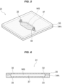
FIG. 5 is a perspective view of a main chip according to a second embodiment; -
FIG. 6 is a vertical cross-sectional view of the main chip according to the second embodiment; -
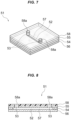
FIG. 7 is a perspective view of a joint chip according to the first embodiment; -
FIG. 8 is a vertical cross-sectional view of the joint chip according to the first embodiment; -
FIG. 9 is a perspective view of a joint chip according to the second embodiment; -
FIG. 10 is a vertical cross-sectional view of the joint chip according to the second embodiment; -
FIG. 11 is a perspective view of a guide; -
FIG. 12 is a perspective view of a microfluidic chip according to the first embodiment; -
FIG. 13 is a perspective view of a microfluidic chip according to the second embodiment; -
FIG. 14 is a schematic view illustrating the microfluidic chip according to the first embodiment with the guide excluded; -
FIG. 15 is a schematic view illustrating the microfluidic chip according to the second embodiment with the guide excluded; -
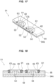
FIG. 16 is a perspective view of a joint chip illustrating another embodiment of a seal structure; -
FIG. 17 is a perspective view illustrating the joint chip in vertical section; -
FIG. 18 is a vertical cross-sectional view of the joint chip; and -
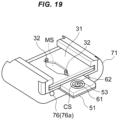
FIG. 19 is a perspective view of a microfluidic chip. - Embodiments will be described with reference to the accompanying drawings. The description will be made along the following items.
- 1. Configuration
- (1) overall outline
- (2) main chip
- (first aspect)
- (second aspect)
- (common matters)
- (3) joint chip
- (first aspect)
- (second aspect)
- (common matters)
- (4) guide
- (5) microfluidic chip
- (6) another embodiment of seal structure
- 2. Actions and effects
- (1) actions
- (2) effects
- 3. Modifications
- As illustrated in
FIG. 1 , amicrofluidic device 101 according to the present embodiment is configured with a plurality ofmicrofluidic chips 11 connected in a row. Each individualmicrofluidic chip 11 mainly has amain chip 31 which is internally provided with a minute space MS such as a microchannel or a reaction vessel, and has a structure in which themain chip 31 is held together with ajoint chip 51 by a guide 71 (refer toFIGS. 2 and12 ). - An X direction in
FIG. 1 is the direction of arrangement of themicrofluidic chips 11 and defines the length direction of each element. "Both ends" and "ends" of themicrofluidic device 101,microfluidic chip 11,main chip 31,joint chip 51, and guide 71 mean both ends and ends in the X direction, respectively. - A Y direction in
FIG. 1 is the direction perpendicular to the direction of arrangement of themicrofluidic chips 11 and defines the width direction of each element. "Both side ends" and "side parts" of themicrofluidic device 101,microfluidic chip 11,main chip 31,joint chip 51, and guide 71 mean both side ends and side parts in the Y direction, respectively. - A Z direction in
FIG. 1 defines the vertical direction of themicrofluidic device 101,microfluidic chip 11,main chip 31,joint chip 51, and guide 71. The top surface appears above as viewed in the Z direction inFIG. 1 , and the bottom surface appears below as viewed in the Z direction inFIG. 1 . - As schematically illustrated in
FIG. 2 , themain chip 31 has the same length (length in the X direction) as theguide 71, and is held by theguide 71 without protruding therefrom. Therefore, when the individualmicrofluidic chips 11 are arranged in a row and connected, themain chips 31 and guides 71 included in the two adjacentmicrofluidic chips 11 are in contact with each other at both end surfaces thereof. In the present embodiment, the mutually contacting end surfaces of the two adjacent microfluidic guides 71 are referred to as mounting surfaces 72 (refer toFIG. 11 ). - The
joint chip 51 is arranged in a stack on the two adjacentmain chips 31 so as to straddle them. - In the
guide 71, the area to hold themain chip 31 is anupper holding area 73, and the area to hold thejoint chip 51 is a lower holding area 74 (refer toFIG. 11 ). When themain chip 31 is correctly held in theupper holding area 73, and thejoint chip 51 is correctly held in thelower holding area 74, themain chip 31 and thejoint chip 51 are positioned in a stacked and contacting state as illustrated inFIG. 2 . - When the individual
microfluidic chips 11 are connected in a row, a flow channel FC including the minute space MS is formed. The following elements form the flow channel FC. - ▪ Minute space MS of
main chip 31, - ▪ A pair of supply holes 32 of
main chip 31, - ▪ A pair of main communication holes 33 of
main chip 31, - ▪ A
communication flow path 52 ofjoint chip 51, and - ▪ A pair of joint communication holes 53 of
joint chip 51 - When a liquid serving as a sample is introduced from the
supply hole 32 of themain chip 31 when a plurality ofmicrofluidic chips 11 are connected in a row to configure amicrofluidic device 101, the liquid flows through the flow channel FC. - However, among the elements forming the flow channel FC, the
supply hole 32 is essential from the perspective of the entire structure of themicrofluidic device 101, but when viewed on the individualmicrofluidic chip 11 basis, thesupply hole 32 is not essential for allmicrofluidic chips 11. Therefore, themain chips 31 include a type provided with thesupply hole 32 and a type without thesupply hole 32, which are mixed together. - In
FIG. 1 , the twomain chips 31 on the front side are of a type havingsupply holes 32, and the twomain chips 31 on the back side are of a type without supply holes 32. Thus, when assembling themicrofluidic device 101 by combining the desiredmain chips 31, it is possible to appropriately combine themain chips 31 each having thesupply hole 32 and themain chips 31 each having nosupply hole 32. - Hereinafter, for convenience of explanation, the
main chip 31 provided with the supply holes 32 will be described as an example, but allmain chips 31 are not provided with the supply holes 32. As for themain chip 31 of type with no supply holes 32, please note that the supply holes 32 are eliminated from themain chip 31 introduced below. - A first aspect of the
main chip 31 is illustrated inFIGS. 3 and 4 . Themain chip 31 is a rectangular-shaped plate-like substrate, and is configured by stacking three acrylic plates each having translucency. They are three of a middle layermain substrate 34, an upper layermain substrate 35, and a lower layermain substrate 36. Themain chip 31 is manufactured by positioning the upper layermain substrate 35 on an upper surface of the middle layermain substrate 34 and the lower layermain substrate 36 on a lower surface thereof respectively and thermocompression-bonding them. - All three acrylic plates (34, 35, and 36) use the same shape and size with a 20 mm square. The thickness of the middle layer
main substrate 34 is 0.5 mm, the thickness of the upper layermain substrate 35 is 1.0 mm, and the thickness of the lower layermain substrate 36 is 0.5 mm. - The middle layer
main substrate 34 is provided with an openingportion 37 which becomes a minute space MS. The shape of the minute space MS defined by the openingportion 37 can be determined as appropriate depending on the use of each individualmicrofluidic chip 11. - The upper layer
main substrate 35 is provided on both end sides with a pair of supply holes 32 communicating with the minute space MS. - The lower layer
main substrate 36 is provided on both end sides with a pair of main communication holes 33 communicating with the minute space MS. - The
main chip 31, which is completed by thermocompression-bonding the three stacked acrylic plates (34, 35, and 36), has a form in which the minute space MS can be visually recognized from the outside as illustrated inFIG. 1 . - The
main chip 31 of the type having no supply holes 32 can be manufactured in the same manner by using the plain upper layermain substrate 35 having no supply holes 32. - A second aspect of the
main chip 31 is illustrated inFIGS. 5 and 6 . Themain chip 31 is a rectangular-shaped plate-like substrate, and is configured by stacking two acrylic plates each having translucency. They are two of amain substrate 34A and an upper layermain substrate 35. Themain chip 31 is manufactured by positioning the upper layermain substrate 35 on an upper surface of themain substrate 34A and bonding it by thermocompression. - Both of the two acrylic plates (34A and 35) forming the two layers use the same shape and size with a 20 mm square. The thickness of both the
main substrate 34A and the upper layermain substrate 35 is 1.0 mm. - The
main substrate 34A is provided with a minute space MS and a pair of main communication holes 33. The shape of the minute space MS can be determined as appropriate depending on the use of each individualmicrofluidic chip 11. As for the pair of main communication holes 33, they are provided on both end sides of themain chip 31 so as to communicate with the lower surface of themain substrate 34A. - The upper layer
main substrate 35 is provided with a pair of supply holes 32 on both end sides thereof, which communicates with the minute space MS. - The
main chip 31, which is completed by thermocompression-bonding the two stacked acrylic plates (34A and 35), has a form in which the minute space MS can be visually recognized from the outside as illustrated inFIG. 1 . - The
main chip 31 of the type having no supply holes 32 can be manufactured in the same manner by using the plain upper layermain substrate 35 having no supply holes 32. - In implementation, a plurality of types of standardized
main chips 31 having various types of minute spaces MS each having a typical shape of a flow path or a reaction vessel may be prepared in advance so that an appropriate selection can be made. Themain chip 31 having the supply holes 32 and themain chip 31 having no supply holes 32 can also be similarly standardized. When a minute space MS which is not prepared in advance is required, a main chip 31 (dedicated part) having such a minute space MS is manufactured each time. - The middle layer
main substrate 34 and the lower layermain substrate 36 in the first aspect conceptually correspond to themain substrate 34A in the second aspect. In the first aspect, the two acrylic plates (34, 36) are stacked and bonded to generate themain substrate 34A (middle layermain substrate 34, lower layer main substrate 36), and in the second aspect, the single acrylic plate (34A) is used to generate themain substrate 34A (middle layer main substrate34, lower layer main substrate 36). Therefore, it can be said that the difference between the first aspect and the second aspect resides in the method of manufacturing themain substrate 34A. - In terms of such a difference in manufacturing method, it is also possible to integrally shape the
main substrate 34A and the upper layermain substrate 35. As an example, a 3D printer can be used to realize an integrally shaped product of themain substrate 34A and the upper layermain substrate 35. A support material is provided in advance in the portions which become the minute space MS, thesupply hole 32, and the pair of main communication holes 33 to create modeling inclusive of the support material as well. By removing the support material after the modeling is completed, a plate-shapedmain chip 31 is completed which has the minute space MS thereinside and has thesupply hole 32 communicating with the minute space MS on its upper surface, and which has the pair of main communication holes 33 on both end sides of its lower surface, which communicates with the minute space MS. - In the present embodiment, there has been shown an example in which the
main chip 31 is made of one or more acrylic plates (34 to 36, 34A, and 35), that is, an acrylic resin, but themain chip 31 may be manufactured using as materials, such as polydimethylsiloxane (PDMS), glass, polycarbonate (PC), polyethylene terephthalate (PET), cycloolefin polymer (COP) without being limited to the acrylic resin. In addition to the above, themain chip 31 can be manufactured using various types of materials such as an ABS resin, a PLA resin, an ASA resin (strong in weather resistance), a PP resin (strong in heat resistance and chemical resistance), a PC resin, a nylon resin, an acrylic resin, PETG, thermoplastic polyurethane. - A first aspect of the
joint chip 51 is illustrated inFIGS. 7 and 8 . Thejoint chip 51 is a rectangular-shaped plate-like substrate, and is configured by stacking three acrylic plates each having translucency. They are three of a middle layerjoint substrate 54, an upper layerjoint substrate 55, and a lower layerjoint substrate 56. Thejoint chip 51 is manufactured by positioning the upper layerjoint substrate 55 on an upper surface of the middle layerjoint substrate 54, and the lower layerjoint substrate 56 on its lower surface and bonding them by thermocompression, respectively. - The three acrylic plates (54, 55, and 56) forming the three layers all use the same shape and size with a 10 mm square. They all have the same thickness: the middle layer
joint substrate 54 has a thickness of 0.5 mm, the upper layerjoint substrate 55 has a thickness of 0.5 mm, and the lower layerjoint substrate 56 also has a thickness of 0.5 mm. - The middle layer
joint substrate 54 is provided with an openingportion 57 which becomes acommunication flow path 52. - The upper layer
joint substrate 55 is provided on both end sides with a pair of joint communication holes 53 communicating with thecommunication flow path 52. - The lower layer
joint substrate 56 is a plain acrylic plate with no holes or openings formed therein. - A
rubber sheet 58 is bonded to the upper surface of thejoint chip 51 completed by thermocompression-bonding the three stacked acrylic plates (54, 55, and 56), i.e., the surface of the upper layerjoint substrate 55. The bonding of therubber sheet 58 to the surface of the upper layerjoint substrate 55 is performed by, for example, adhesion. Therubber sheet 58 has the same size and shape as the three acrylic plates (54, 55, and 56) and is bonded thereto without being protruded or displaced from these acrylic plates (54, 55, and 56). - The
rubber sheet 58 is provided with a pair of throughholes 58a in position alignment with these joint communication holes 53 so as not to block the pair of joint communication holes 53 provided on both end sides of the upper layerjoint substrate 55. - A second aspect of the
joint chip 51 is illustrated inFIGS. 9 and 10 . Thejoint chip 51 is a rectangular-shaped plate-like substrate, and is configured by stacking two acrylic plates each having translucency. They are two of ajoint substrate 54A and an upper layerjoint substrate 55. Thejoint chip 51 is manufactured by positioning the upper layerjoint substrate 55 on an upper surface of thejoint substrate 54A and bonding the same by thermocompression. - The two acrylic plates (54A and 55) forming the two layers use the same shape and size, both of which are a 10 mm square. The
joint substrate 54A is 1.0 mm in thickness, and the upper layerjoint substrate 55 is 0.5 mm in thickness. - The
joint substrate 54A is provided with acommunication flow path 52. - The upper layer
joint substrate 55 is provided on both end sides with a pair of joint communication holes 53 communicating with thecommunication flow path 52. - A
rubber sheet 58 is bonded to the upper surface of thejoint chip 51 completed by thermocompression-bonding the two stacked acrylic plates (54A and 55), i.e., the surface of the upper layerjoint substrate 55. The bonding of therubber sheet 58 to the surface of the upper layerjoint substrate 55 is performed by, for example, adhesion. Therubber sheet 58 has the same size and shape as the two acrylic plates (54A and 55) and is bonded thereto without being protruded or displaced from these acrylic plates (54A and 55). - The
rubber sheet 58 is provided with a pair of throughholes 58a in position alignment with the pair of joint communication holes 53 so as not to block these joint communication holes 53 provided on both end sides of the upper layerjoint substrate 55. - The middle layer
joint substrate 54 and the lower layerjoint substrate 56 in the first aspect conceptually correspond to thejoint substrate 54A in the second aspect. In the first aspect, the two acrylic plates (54 and 56) are stacked and bonded to generate thejoint substrate 54A (middle layerjoint substrate 54, lower layer joint substrate 56), and in the second aspect, the single acrylic plate (54A) is used to generate thejoint substrate 54A (middle layerjoint substrate 54, lower layer joint substrate 56), respectively. Therefore, it can be said that the difference between the first aspect and the second aspect resides in the method of manufacturing thejoint substrate 54A. - In terms of such a difference in manufacturing method, it is also possible to integrally shape the
joint substrate 54A and the upper layerjoint substrate 55. As an example, a 3D printer can be used to realize an integrally shaped product of thejoint substrate 54A and the upper layerjoint substrate 55. A support material is provided in advance in the portions which become thecommunication flow path 52 and the pair of joint communication holes 53 to create modeling inclusive of the support material as well. By removing the support material after the modeling is completed, a plate-shapedjoint chip 51 is completed which has thecommunication flow path 52 thereinside and has on both end sides of its upper surface, the pair of joint communication holes 53 for allowing thecommunication flow path 52 to communicate with the minute space MS. - In the present embodiment, there has been shown an example in which the
joint chip 51 is made of one or more acrylic plates (54 to 56, 54A, and 55), that is, an acrylic resin, but thejoint chip 51 may be manufactured using as materials, such as polydimethylsiloxane (PDMS), glass, polycarbonate (PC), polyethylene terephthalate (PET), cycloolefin polymer (COP) without being limited to the acrylic resin. In addition to the above, thejoint chip 51 can be manufactured using various types of materials such as an ABS resin, a PLA resin, an ASA resin (strong in weather resistance), a PP resin (strong in heat resistance and chemical resistance), a PC resin, a nylon resin, an acrylic resin, PETG, thermoplastic polyurethane. - As illustrated in
FIG. 11 , theguide 71 is shaped from, for example, a resin material, and includes theupper holding area 73 whose upper surface is made open, and the pair oflower holding areas 74 on both end sides of theupper holding area 73. - When viewed from the sides of the mounting
surfaces 72 located at both ends of theguide 71, the upper portions of both side walls of theupper holding area 73 overhang to face each other to thereby configure a pair ofrails 75 which guides the sliding movement of themain chip 31. Themain chip 31 is inserted from the mountingsurface 72 along theserails 75 and is housed and held in theupper holding area 73. Themain chip 31 housed in theupper holding area 73 exposes the minute space MS to the outside from the space between the pair ofrails 75, thereby enabling visual recognition and processing operations from the outside. - The pair of
lower holding areas 74 are in communication with the mountingsurface 72 in a form which is one step lower than the bottom surface of theupper holding area 73. Therefore, thelower holding area 74 opens toward the mountingsurface 72 while themain chip 31 is held in theupper holding area 73 and receives mounting of thejoint chip 51 by sliding movement. The depth of thelower holding area 74 is set to be half the length of thejoint chip 51. - As described above, the multiple
microfluidic chips 11 can be connected in their length directions (X direction inFIG. 1 ). Connectingportions 76 provided in the mountingsurface 72 of theguide 71 realizes such a connection between themicrofluidic chips 11. The connectingportions 76 are configured by a plurality ofmagnets 76a embedded into the mountingsurface 72. - In the present embodiment, the connection of each
individual guide 71 is given directionality. For example, when oneguide 71 and anotherguide 71 are connected, the surfaces to be joined facing each other are determined beforehand. For convenience of explanation, the visible surface located on the front side inFIG. 11 is referred to as the mountingsurface 72A, and the invisible surface on the deep side is referred to as the mountingsurface 72B. On this premise, when the twoguides 71 are connected, the mountingsurface 72B of anotherguide 71 is connected to the mountingsurface 72A of oneguide 71, and the mountingsurface 72A of anotherguide 71 is connected to the mountingsurface 72B of oneguide 71. - Therefore, in the connecting
portion 76, themagnet 76a embedded in the mountingsurface 72A is made different in polarity from themagnet 76a embedded in the mountingsurface 72B. As a result, themagnets 76a attract each other with a magnetic force, and the twoguides 71 can be connected in a fixed state. - The
guide 71 further has arestriction part 77 as well. Therestriction part 77 has a structure which restricts the positional displacements of the twoguides 71 in a stacking direction of themain chip 31 and thejoint chip 51 when the twoguides 71 are connected to each other. Such arestriction part 77 is configured by aconvex step portion 77a provided on the mountingsurface 72A and aconcave step portion 77b provided on the mountingsurface 72B. Theconvex step portion 77a protrudes from the mountingsurface 72A in the length direction (X direction inFIG. 1 ). Theconcave step portion 77b retracts from the mountingsurface 72B in the length direction so that they fit into each other. - When the two
guides 71 are connected, theconvex step portion 77a of oneguide 71 fits into theconcave step portion 77b of anotherguide 71, or theconcave step portion 77b of oneguide 71 fits to theconvex step portion 77a of anotherguide 71 to thereby restrict the positional displacements of the twoguides 71 in the stacking direction of themain chip 31 and thejoint chip 51. -
FIG. 12 is a perspective view of themicrofluidic chip 11 according to the first embodiment using themain chip 31 and thejoint chip 51 in the first embodiment, andFIG. 14 is a schematic view illustrating themicrofluidic chip 11 according to the first embodiment with theguide 71 excluded.FIG. 13 is a perspective view of amicrofluidic chip 11 according to a second embodiment using amain chip 31 and ajoint chip 51 in the second embodiment, andFIG. 15 is a schematic view illustrating themicrofluidic chip 11 according to the second embodiment with aguide 71 excluded. - As illustrated in
FIGS. 12 and13 , themicrofluidic chip 11 is assembled by mounting themain chip 31 on theupper holding area 73 of theguide 71 and mounting thejoint chip 51 on thelower holding area 74. Thejoint chip 51 is inserted and held in thelower holding area 74 by half its length, and the remaining half becomes in a state of protruding from the mountingsurface 72. This protruding half ofjoint chip 51 is inserted and held in alower holding area 74 provided in aguide 71 of anothermicrofluidic chip 11 connected to themicrofluidic chip 11. - Then, as illustrated in
FIGS. 14 and15 , themain chip 31 and thejoint chip 51 are stacked, and the respective minute spaces MS of the twomicrofluidic chips 11 are connected to thejoint chip 51 to form a flow channel FC. - More specifically, a
joint communication hole 53 provided in an upper layerjoint substrate 55 of thejoint chip 51 communicates with amain communication hole 33 provided in a lower layermain substrate 36 of themain chip 31. Thus, the respective minute spaces MS of the twomicrofluidic chips 11 are in communication via themain communication hole 33 of onemicrofluidic chip 11, thejoint communication hole 53 on one end side of thejoint chip 51 straddling the twomicrofluidic chips 11, thecommunication flow path 52, thejoint communication hole 53 on the opposite end side thereof, and themain communication hole 33 of the othermicrofluidic chip 11. - When forming such a flow channel FC, the gap between the stacked
main chip 31 andjoint chip 51 is sealed by arubber sheet 58 provided on the upper surface of thejoint chip 51 so that the liquid flowing through the flow channel FC is prevented from leaking. - The seal structure which seals the flow channel FC between the
main chip 31 and thejoint chip 51 is not limited to the structure using therubber sheet 58, but can also be achieved by a structure using an O-ring 61. - As illustrated in
FIGS. 16 to 18 , the upper layerjoint substrate 55 of thejoint chip 51 is provided with anannular recess 62 so as to surround the circumferences of the pair of joint communication holes 53. When themain chip 31 and thejoint chip 51 are held in theupper holding area 73 and thelower holding area 74 of theguide 71, respectively, and thejoint chip 51 is superimposed on themain chip 31, therecess 62 forms a communication space CS in which thejoint communication hole 53 and themain communication hole 33 connected to each other are located. - The O-
ring 61 is fitted into aninner wall 63 forming therecess 62 and slightly protrudes from the surface of the upper layerjoint substrate 55, so that the O-ring 61 is brought into contact with the lower layer main substrate 36 (first embodiment) of themain chip 31 or themain substrate 34A thereof (second embodiment). Consequently, the O-ring 61 seals the communication space CS and prevents leakage of the liquid flowing through the flow channel FC at the connecting portion between themain chip 31 and thejoint chip 51. - As illustrated in
FIGS. 17 and 18 , the outer diameter of the O-ring 61 is larger than the inner diameter of therecess 62. The O-ring 61 fitted into theinner wall 63 of therecess 62 is in a state of being elastically deformed and bit into therecess 62. - As illustrated in
FIG. 19 , when themain chip 31 is mounted on theupper holding area 73 of theguide 71, and thejoint chip 51 is mounted on thelower holding area 74, themicrofluidic chip 11 is assembled. Thejoint chip 51 is inserted and held in thelower holding area 74 by half its length, and the remaining half becomes into a state of being protruded from the mountingsurface 72. The protruded half of thejoint chip 51 is inserted and held in thelower holding area 74 provided in theguide 71 of anothermicrofluidic chip 11 connected to themicrofluidic chip 11. Thus, the upper layerjoint substrate 55 of thejoint chip 51 protruding from theguide 71 exposes the O-ring 61 for connection with anothermain chip 31 held in theguide 71 of anothermicrofluidic chip 11. - The seal structure using the O-
ring 61 is applicable even to both themicrofluidic chip 11 in the first embodiment and themicrofluidic chip 11 in the second embodiment. - When the
microfluidic device 101 is required, the combination of themicrofluidic chips 11 each having the minute space MS suitable for the application is planned, and themicrofluidic chips 11 are connected in one row to assemble themicrofluidic device 101. When themicrofluidic device 101 is used, a liquid such as a culture solution or a reagent is injected into thesupply hole 32 prepared on the upper surface of themain chip 31 using an unillustrated pipe or syringe, and the like. Then, the liquid flows through the flow channel FC, and it becomes possible to perform processing such as liquid separation, stirring, heat treatment, fluorescence detection according to the selected minute space MS. - The
microfluidic device 101 according to the present embodiment has the following effects. - The
main chips 31 having the multiple types of minute spaces MS can be rearranged as desired, and the flow channel FC according to the purpose can be easily assembled. At this time, if the flow channel FC can be realized only by combining themain chips 31 each having the standardized minute space MS, the flow channel FC according to the purpose can be created on the spot without preparing special parts. - If the
main chips 31 are classified and prepared according to their functions, it is possible to easily perform operations such as surface treatment depending on the purpose of research. - Since all the
main chips 31 to be connected are arranged on the same plane, the state of each of the minute spaces MS included in all themain chips 31 can be visually observed, and processing such as fluorescence detection using an optical sensor can also be performed. - There is no limit to the number of the
microfluidic chips 11 which can be connected, and excellent expandability can be obtained. In addition, themicrofluidic chip 11 can be expanded simply by inserting themain chip 31 and thejoint chip 51 from the mountingsurface 72 of theguide 71 and connecting the twoguides 71, and the workability for expansion is good. - Since the portions constituting the flow channel FC are in an opened state even in the
main chip 31 and thejoint chip 51, it is easy to clean the inside thereof. - Both the
main chip 31 and thejoint chip 51 can be easily manufactured simply by stacking and joining the acrylic plates (34, 35, 36, 54, 55, and 56). - Since the space between the
main chip 31 and thejoint chip 51 can be sealed with therubber sheet 58, it is possible to prevent the leakage of a liquid. Further, when the twoguides 71 are connected, the positional displacements of themain chip 31 and thejoint chip 51 in the stacking direction thereof can be restricted by therestriction part 77, and from this viewpoint as well, the leakage of the liquid can be prevented. - The two guides 71 can be easily connected by attraction using the magnetic force of the
magnet 76a, and the assembly of themicrofluidic device 101 can be facilitated. - Various modifications and changes can be made in implementation.
- For example, in the
microfluidic chip 11 of the first embodiment, although the specific values for the size and thickness have been given for the three-layer acrylic plates (34, 35, 36, 54, 55, and 56) constituting themain chip 31 and thejoint chip 51, they are merely examples. In implementing, themain chip 31 and thejoint chip 51 can be manufactured using acrylic plates (34, 35, 36, 54, 55, and 56) of various sizes and thicknesses. - This point is also the same for the
microfluidic chip 11 in the second embodiment. The specific values for the size and thickness for the two-layer acrylic plates (34A, 35, 54A and 55) constituting themain chip 31 and thejoint chip 51 are merely examples. In implementing, themain chip 31 and thejoint chip 51 can be manufactured using acrylic plates (34A, 35, 54A, and 55) of various sizes and thicknesses. - The
main chip 31 and thejoint chip 51 do not necessarily have to be manufactured by the acrylic plates. Themain chip 31 and thejoint chip 51 may be manufactured using other types of resin materials, glass, or the like. - The method for joining the acrylic plates is not limited to the thermocompression bonding either, and other methods such as bonding using an adhesive, vacuum compression bonding, and the like may be used.
- The connecting
portion 76 connecting the twoguides 71 may be realized not only by the attraction of themagnets 76a made different in polarity, but also by the magnetic attraction of themagnets 76a to a metal plate, for example. Alternatively, it is not limited themagnets 76a, but any connection structure for connecting two members, such as screwing or clamping, can be applied. - In the above embodiment, the configuration example in which the
main chip 31 and thejoint chip 51 in the first embodiment are combined has been introduced as themicrofluidic chip 11 of the first embodiment, and the configuration example in which themain chip 31 and thejoint chip 51 in the second embodiment are combined has been introduced as themicrofluidic chip 11 of the second embodiment. The implementation is not limited to this, and themain chip 31 of the first embodiment and thejoint chip 51 of the second embodiment, or themain chip 31 of the second embodiment and thejoint chip 51 of the first embodiment may be combined to configure themicrofluidic chip 11. - Further, the
microfluidic device 101 can be configured by freely combining themain chip 31 and thejoint chip 51 in the first embodiment, themain chip 31 and thejoint chip 51 in the second embodiment, the seal structure using therubber sheet 58, the seal structure using the O-ring 61, and various modifications and changes of these. - All other modifications and changes are permitted.
-
- 11
- microfluidic chip
- 31
- main chip
- 32
- supply hole
- 33
- main communication hole
- 34A
- main substrate
- 34
- middle layer main substrate
- 35
- upper layer main substrate
- 36
- lower layer main substrate
- 37
- opening portion
- 51
- joint chip
- 52
- communication flow path
- 53
- joint communication hole
- 54A
- joint substrate
- 54
- middle layer joint substrate
- 55
- upper layer joint substrate
- 56
- lower layer joint substrate
- 57
- opening portion
- 58
- rubber sheet
- 58a
- through hole
- 61
- O-ring
- 62
- recess
- 63
- inner wall
- 71
- guide
- 72, 72A, 72B
- mounting surface
- 73
- upper holding area
- 74
- lower holding area
- 75
- rail
- 76
- connecting portion
- 76a
- magnet
- 77
- restriction part
- 77a
- convex step portion
- 77b
- concave step portion
- 101
- microfluidic device
- CS
- communication space
- FC
- flow channel
- MS
- minute space
Claims (18)
- A microfluidic device comprising:a plate-shaped main chip having a minute space inside into which a liquid is introduced;a plate-shaped joint chip having a communication flow path inside and having on both end sides of an upper surface of the joint chip, a pair of joint communication holes for communicating the communication flow path to the minute space; anda guide having an upper holding area which holds the main chip, and a lower holding area which selectively holds one of both ends of the joint chip while being partially stacked on the main chip held in the upper holding area,wherein the main chip includes a pair of main communication holes on both end sides of a lower surface of the main chip, the pair of main communication holes communicating the minute space with the joint communication hole of the joint chip held in the lower holding area while being held in the upper holding area.
- The microfluidic device according to claim 1, wherein the main chip has a supply hole for liquid supply on an upper surface of the main chip, the supply hole communicating with the minute space.
- The microfluidic device according to claim 1, wherein the main chip has an upper layer main substrate bonded to an upper surface of a main substrate having the minute space and the pair of main communication holes.
- The microfluidic device according to claim 1, wherein the main chip has an upper layer main substrate having the supply hole, which is bonded to the upper surface of the main substrate having the minute space and the pair of main communication holes.
- The microfluidic device according to claim 3, wherein the main substrate includes:a middle layer main substrate having an opening portion serving as the minute space, anda lower layer main substrate having the pair of main communication holes communicating with the opening portion and bonded to a lower surface of the middle layer main substrate so as to close the opening portion which serves as the minute space.
- The microfluidic device according to claim 3, wherein the main substrate integrally has the minute space and the pair of main communication holes.
- The microfluidic device according to claim 3, wherein the upper layer main substrate has translucency, and
wherein the guide holds the main chip in the upper holding area with the upper layer main substrate exposed. - The microfluidic device according to claim 7, wherein the main substrate and the upper layer main substrate are acrylic plates.
- The microfluidic device according to claim 1, wherein the joint chip has an upper layer joint substrate having the pair of joint communication holes, which is bonded to an upper surface of a joint substrate having the communication flow path.
- The microfluidic device according to claim 9, wherein the joint substrate includes:a middle layer joint substrate having an opening portion serving as the communication flow path, anda lower layer joint substrate bonded to a lower surface of the middle layer joint substrate so as to close the opening portion serving as the communication flow path.
- The microfluidic device according to claim 9, wherein the joint substrate integrally has the communication flow path.
- The microfluidic device according to claim 9, wherein the joint substrate and the upper layer joint substrate are acrylic plates.
- The microfluidic device according to claim 1, wherein the joint chip has a rubber sheet on an upper surface of the joint chip, and
wherein the rubber sheet has a through hole at the position of the joint communication hole. - The microfluidic device according to claim 1, wherein the joint chip has an O-ring surrounding the joint communication hole on an upper surface of the joint chip, and
wherein the O-ring seals a communication space in which the joint communication hole and the main communication hole which communicate with each other are located. - The microfluidic device according to claim 1, wherein the guide has a mounting surface on an end surface which holds the joint chip, and
wherein the guide enables the main chip and the joint chip to be inserted from the mounting surface and mounted in the upper holding area and the lower holding area, respectively. - The microfluidic device according to claim 15, wherein the guide holds the main chip in the upper holding area without protruding, and
wherein the guide has a connecting portion which detachably connects the mutually facing mounting surfaces of the guide which holds one end of one of the joint chips and the other guide which holds the opposite end of the joint chip. - The microfluidic device according to claim 16, wherein the connecting portion connects the mounting surfaces of the two guides by the magnetic force of a magnet embedded in the mounting surface.
- The microfluidic device according to claim 16, wherein the two guides connected to each other each have a restriction part which restricts positional displacements of the two guides in a stacking direction of the main chip and the joint chip.
Applications Claiming Priority (2)
| Application Number | Priority Date | Filing Date | Title |
|---|---|---|---|
| JP2022106726 | 2022-06-30 | ||
| PCT/JP2023/022276 WO2024004685A1 (en) | 2022-06-30 | 2023-06-15 | Microfluidic device |
Publications (2)
| Publication Number | Publication Date |
|---|---|
| EP4549371A1 true EP4549371A1 (en) | 2025-05-07 |
| EP4549371A4 EP4549371A4 (en) | 2026-02-11 |
Family
ID=89382155
Family Applications (1)
| Application Number | Title | Priority Date | Filing Date |
|---|---|---|---|
| EP23831133.6A Pending EP4549371A4 (en) | 2022-06-30 | 2023-06-15 | MICROFLUIDIC DEVICE |
Country Status (5)
| Country | Link |
|---|---|
| US (1) | US20250312790A1 (en) |
| EP (1) | EP4549371A4 (en) |
| JP (1) | JP7527529B2 (en) |
| CN (1) | CN119110789A (en) |
| WO (1) | WO2024004685A1 (en) |
Families Citing this family (2)
| Publication number | Priority date | Publication date | Assignee | Title |
|---|---|---|---|---|
| CN118925817B (en) * | 2024-07-26 | 2025-12-26 | 哈尔滨工业大学 | A microfluidic chip and a clamping fixture for the microfluidic chip. |
| JP7721776B1 (en) * | 2024-12-16 | 2025-08-12 | 株式会社神鋼環境ソリューション | Fluid flow path device and method for manufacturing fluid flow path device |
Family Cites Families (13)
| Publication number | Priority date | Publication date | Assignee | Title |
|---|---|---|---|---|
| JP2001194373A (en) * | 2000-01-06 | 2001-07-19 | Olympus Optical Co Ltd | Microminiature chemical operator |
| US7485454B1 (en) * | 2000-03-10 | 2009-02-03 | Bioprocessors Corp. | Microreactor |
| US6848462B2 (en) * | 2001-12-06 | 2005-02-01 | Nanostream, Inc. | Adhesiveless microfluidic device fabrication |
| AU2002353107A1 (en) * | 2001-12-11 | 2003-07-09 | Sau Lan Tang Staats | Microfluidic devices and methods for two-dimensional separations |
| JP2005147940A (en) | 2003-11-18 | 2005-06-09 | Enplas Corp | Microfluidic device |
| US7011793B2 (en) * | 2003-05-15 | 2006-03-14 | Kionix, Inc. | Reconfigurable modular microfluidic system and method of fabrication |
| JP4728573B2 (en) * | 2003-11-28 | 2011-07-20 | 古河電気工業株式会社 | Micro chemical reactor |
| JP2005214741A (en) * | 2004-01-28 | 2005-08-11 | Jasco Corp | Microchip |
| JP4552673B2 (en) * | 2005-02-01 | 2010-09-29 | 株式会社豊田中央研究所 | Light immobilization method for minute objects |
| US7919062B2 (en) * | 2008-03-20 | 2011-04-05 | Corning Incorporated | Modular microfluidic system and method for building a modular microfludic system |
| JP6272023B2 (en) | 2013-12-26 | 2018-01-31 | 高砂電気工業株式会社 | Microfluidic chip device |
| US9795963B2 (en) * | 2014-09-26 | 2017-10-24 | Picosys Incorporated | Method and apparatus for taped interlayer flow cell with masking and conductive traces |
| WO2019092989A1 (en) | 2017-11-10 | 2019-05-16 | Nok株式会社 | Microfluidic chip and microfluidic device |
-
2023
- 2023-06-15 JP JP2024530688A patent/JP7527529B2/en active Active
- 2023-06-15 CN CN202380035772.6A patent/CN119110789A/en active Pending
- 2023-06-15 EP EP23831133.6A patent/EP4549371A4/en active Pending
- 2023-06-15 WO PCT/JP2023/022276 patent/WO2024004685A1/en not_active Ceased
- 2023-06-15 US US18/870,081 patent/US20250312790A1/en active Pending
Also Published As
| Publication number | Publication date |
|---|---|
| EP4549371A4 (en) | 2026-02-11 |
| CN119110789A (en) | 2024-12-10 |
| JPWO2024004685A1 (en) | 2024-01-04 |
| JP7527529B2 (en) | 2024-08-02 |
| WO2024004685A1 (en) | 2024-01-04 |
| US20250312790A1 (en) | 2025-10-09 |
Similar Documents
| Publication | Publication Date | Title |
|---|---|---|
| US8763642B2 (en) | Microfluidic devices with mechanically-sealed diaphragm valves | |
| US20250312790A1 (en) | Microfluidic device | |
| KR102514793B1 (en) | Modular micro-fluidic chip and micro-fluidic flow system having thereof | |
| US9101930B2 (en) | Microfluidic cartridge for processing and detecting nucleic acids | |
| US12064761B2 (en) | Flow cell with flexible connection | |
| CN111050913A (en) | Injection-molded microfluidics/fluidic cassettes integrated with silicon-based sensors | |
| JP6111161B2 (en) | Fluid handling apparatus and fluid handling method | |
| US20240408597A1 (en) | Flow cell with flexible connection | |
| EP3875574B1 (en) | Micro-fluid chip and micro-fluid device | |
| KR102514771B1 (en) | Modular micro-fluidic chip and micro-fluidic flow system having thereof | |
| US11471883B2 (en) | Fluid chip, fluid device, and method for manufacturing same | |
| JP7470288B2 (en) | Microfluidic Devices | |
| JP2005147940A (en) | Microfluidic device | |
| CN216236966U (en) | Gene detection kit | |
| HK40064510A (en) | Flow cell with flexible connection | |
| HK40017277A (en) | Flow cell with flexible connection | |
| HK40017277B (en) | Flow cell with flexible connection | |
| KR20210085926A (en) | Modular micro-fluidic chip and method for controlling micro-fluid using the same |
Legal Events
| Date | Code | Title | Description |
|---|---|---|---|
| STAA | Information on the status of an ep patent application or granted ep patent |
Free format text: STATUS: THE INTERNATIONAL PUBLICATION HAS BEEN MADE |
|
| PUAI | Public reference made under article 153(3) epc to a published international application that has entered the european phase |
Free format text: ORIGINAL CODE: 0009012 |
|
| STAA | Information on the status of an ep patent application or granted ep patent |
Free format text: STATUS: REQUEST FOR EXAMINATION WAS MADE |
|
| 17P | Request for examination filed |
Effective date: 20241018 |
|
| AK | Designated contracting states |
Kind code of ref document: A1 Designated state(s): AL AT BE BG CH CY CZ DE DK EE ES FI FR GB GR HR HU IE IS IT LI LT LU LV MC ME MK MT NL NO PL PT RO RS SE SI SK SM TR |
|
| DAV | Request for validation of the european patent (deleted) | ||
| DAX | Request for extension of the european patent (deleted) | ||
| A4 | Supplementary search report drawn up and despatched |
Effective date: 20260114 |
|
| RIC1 | Information provided on ipc code assigned before grant |
Ipc: B81B 1/00 20060101AFI20260108BHEP Ipc: B01J 19/00 20060101ALI20260108BHEP Ipc: B81B 7/04 20060101ALI20260108BHEP Ipc: G01N 35/08 20060101ALI20260108BHEP Ipc: G01N 37/00 20060101ALI20260108BHEP Ipc: B01L 3/00 20060101ALN20260108BHEP Ipc: B01L 9/00 20060101ALN20260108BHEP |