EP4546589A1 - Inrush current reduction circuit - Google Patents
Inrush current reduction circuit Download PDFInfo
- Publication number
- EP4546589A1 EP4546589A1 EP24164870.8A EP24164870A EP4546589A1 EP 4546589 A1 EP4546589 A1 EP 4546589A1 EP 24164870 A EP24164870 A EP 24164870A EP 4546589 A1 EP4546589 A1 EP 4546589A1
- Authority
- EP
- European Patent Office
- Prior art keywords
- inrush current
- resistor
- switching element
- reduction circuit
- current reduction
- Prior art date
- Legal status (The legal status is an assumption and is not a legal conclusion. Google has not performed a legal analysis and makes no representation as to the accuracy of the status listed.)
- Pending
Links
Images



Classifications
-
- H—ELECTRICITY
- H02—GENERATION; CONVERSION OR DISTRIBUTION OF ELECTRIC POWER
- H02J—ELECTRIC POWER NETWORKS; CIRCUIT ARRANGEMENTS OR SYSTEMS FOR SUPPLYING OR DISTRIBUTING ELECTRIC POWER; SYSTEMS FOR STORING ELECTRIC ENERGY
- H02J7/00—Circuit arrangements for charging or discharging batteries or for supplying loads from batteries
- H02J7/60—Circuit arrangements for charging or discharging batteries or for supplying loads from batteries including safety or protection arrangements
-
- H—ELECTRICITY
- H02—GENERATION; CONVERSION OR DISTRIBUTION OF ELECTRIC POWER
- H02H—EMERGENCY PROTECTIVE CIRCUIT ARRANGEMENTS
- H02H9/00—Emergency protective circuit arrangements for limiting excess current or voltage without disconnection
- H02H9/001—Emergency protective circuit arrangements for limiting excess current or voltage without disconnection limiting speed of change of electric quantities, e.g. soft switching on or off
-
- H—ELECTRICITY
- H02—GENERATION; CONVERSION OR DISTRIBUTION OF ELECTRIC POWER
- H02H—EMERGENCY PROTECTIVE CIRCUIT ARRANGEMENTS
- H02H9/00—Emergency protective circuit arrangements for limiting excess current or voltage without disconnection
- H02H9/04—Emergency protective circuit arrangements for limiting excess current or voltage without disconnection responsive to excess voltage
-
- H—ELECTRICITY
- H02—GENERATION; CONVERSION OR DISTRIBUTION OF ELECTRIC POWER
- H02J—ELECTRIC POWER NETWORKS; CIRCUIT ARRANGEMENTS OR SYSTEMS FOR SUPPLYING OR DISTRIBUTING ELECTRIC POWER; SYSTEMS FOR STORING ELECTRIC ENERGY
- H02J7/00—Circuit arrangements for charging or discharging batteries or for supplying loads from batteries
- H02J7/60—Circuit arrangements for charging or discharging batteries or for supplying loads from batteries including safety or protection arrangements
- H02J7/62—Circuit arrangements for charging or discharging batteries or for supplying loads from batteries including safety or protection arrangements against overcurrent
-
- H—ELECTRICITY
- H02—GENERATION; CONVERSION OR DISTRIBUTION OF ELECTRIC POWER
- H02H—EMERGENCY PROTECTIVE CIRCUIT ARRANGEMENTS
- H02H3/00—Emergency protective circuit arrangements for automatic disconnection directly responsive to an undesired change from normal electric working condition with or without subsequent reconnection ; integrated protection
- H02H3/08—Emergency protective circuit arrangements for automatic disconnection directly responsive to an undesired change from normal electric working condition with or without subsequent reconnection ; integrated protection responsive to excess current
-
- H—ELECTRICITY
- H02—GENERATION; CONVERSION OR DISTRIBUTION OF ELECTRIC POWER
- H02J—ELECTRIC POWER NETWORKS; CIRCUIT ARRANGEMENTS OR SYSTEMS FOR SUPPLYING OR DISTRIBUTING ELECTRIC POWER; SYSTEMS FOR STORING ELECTRIC ENERGY
- H02J7/00—Circuit arrangements for charging or discharging batteries or for supplying loads from batteries
- H02J7/90—Regulation of charging or discharging current or voltage
- H02J7/94—Regulation of charging or discharging current or voltage in response to battery current
Definitions
- the present invention relates to an inrush current reduction circuit that can reduce generation of an inrush current upon connection of a battery management system (BMS) module to a battery cell module.
- BMS battery management system
- an inrush current generated due to inductance and capacitance components of the BMS module and the battery cell module can cause damage to circuit elements upon connection of the BMS module to the battery cell module.
- an inrush current reduction circuit capable of reducing generation of an inrush current that can be generated upon connection of the BMS module and the battery cell module.
- an inrush current reduction circuit comprises: a switching element connected between a power side of a BMS module and a power side of a battery cell module and having a gate connected to a ground side through a first resistor; a diode connected at one side thereof to a source of the switching element; a second resistor connected at one side thereof to the other side of the diode and connected at the other side thereof to the ground side through the first resistor; and a Zener diode connected in parallel to the second resistor.
- the switching element may include a P-CH field effect transistor (FET).
- FET P-CH field effect transistor
- a drain of the switching element may be connected to the power side of the BMS module.
- the source of the switching element may be connected to the power side of the battery cell module.
- An anode of the diode may be connected to the source of the switching element.
- the Zener diode may be connected between one side of the first resistor and the other side of the diode.
- An anode of the Zener diode may be connected to one side of the first resistor and a cathode of the Zener diode may be connected to a cathode of the diode.
- the switching element may cut off an inrush current generated at an initial stage of connection between the BMS module and the battery cell module in an OFF state and may be turned on to allow only part of the inrush current to flow therethrough using voltage distribution by the first resistor and the second resistor when a voltage (Vgs) between both ends of the second resistor reaches a threshold voltage (Vth) or more, as a voltage level of the inrush current continues to increase.
- Vgs voltage between both ends of the second resistor
- Vth threshold voltage
- the switching element may further include a capacitor and a third resistor connected in parallel to both ends of the switching element.
- the capacitor and the third resistor may be connected in series to the switching element.
- a voltage applied to an input terminal of the switching element may be adjusted depending on capacitance of the capacitor and resistance of the third resistor.
- the inrush current reduction circuit according to the present invention can reduce generation of an inrush current upon connection of a BMS module and a battery cell module.
- the inrush current reduction circuit according to the present invention can prevent damage to circuit elements by reducing generation of an inrush current that can be generated upon connection of the BMS module and the battery cell.
- phrases such as “at least one of A, B and C, “at least one of A, B or C,” “at least one selected from a group of A, B and C,” or “at least one selected from among A, B and C” are used to designate a list of elements A, B and C, the phrase may refer to any and all suitable combinations or a subset of A, B and C, such as A, B, C, A and B, A and C, B and C, or A and B and C.
- the terms “use,” “using,” and “used” may be considered synonymous with the terms “utilize,” “utilizing,” and “utilized,” respectively.
- the terms “substantially,” “about,” and similar terms are used as terms of approximation and not as terms of degree, and are intended to account for the inherent variations in measured or calculated values that would be recognized by those of ordinary skill in the art.
- first, second, third, etc. may be used herein to describe various elements, components, regions, layers, and/or sections, these elements, components, regions, layers, and/or sections should not be limited by these terms. These terms are used to distinguish one element, component, region, layer, or section from another element, component, region, layer, or section. Thus, a first element, component, region, layer, or section discussed below could be termed a second element, component, region, layer, or section without departing from the teachings of example embodiments.
- spatially relative terms such as “beneath,” “below,” “lower,” “above,” “upper,” and the like, may be used herein for ease of description to describe one element or feature's relationship to another element(s) or feature(s) as illustrated in the figures. It will be understood that the spatially relative terms are intended to encompass different orientations of the device in use or operation in addition to the orientation depicted in the figures. For example, if the device in the figures is turned over, elements described as “below” or “beneath” other elements or features would then be oriented “above” or “over” the other elements or features. Thus, the term “below” may encompass both an orientation of above and below. The device may be otherwise oriented (rotated 90 degrees or at other orientations), and the spatially relative descriptors used herein should be interpreted accordingly.
- any numerical range disclosed and/or recited herein is intended to include all sub-ranges of the same numerical precision subsumed within the recited range.
- a range of "1.0 to 10.0" is intended to include all subranges between (and including) the recited minimum value of 1.0 and the recited maximum value of 10.0, that is, having a minimum value equal to or greater than 1.0 and a maximum value equal to or less than 10.0, such as, for example, 2.4 to 7.6.
- Any maximum numerical limitation recited herein is intended to include all lower numerical limitations subsumed therein, and any minimum numerical limitation recited in this specification is intended to include all higher numerical limitations subsumed therein.
- references to two compared elements, features, etc. as being “the same” may mean that they are “substantially the same”.
- the phrase “substantially the same” may include a case having a deviation that is considered low in the art, for example, a deviation of 5% or less.
- a certain parameter when referred to as being uniform in a given region, it may mean that it is uniform in terms of an average.
- an arbitrary element When an arbitrary element is referred to as being disposed (or located or positioned) on the "above (or below)" or “on (or under)” a component, it may mean that the arbitrary element is placed in contact with the upper (or lower) surface of the component and may also mean that another component may be interposed between the component and any arbitrary element disposed (or located or positioned) on (or under) the component.
- FIG. 1 is a circuit diagram of a typical connection circuit between a BMS module 10 and a battery cell module 20.
- an inrush current reduction circuit is not present between the BMS module 10 (only an input side of the BMS module is shown in FIG. 1 for ease of description) and the battery cell module 20.
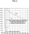
- FIG. 2 is a diagram illustrating an inrush current waveform generated upon connection of the BMS module to the battery cell module in FIG. 1 .
- an inrush current of about 220V is instantaneously generated due to inductance and capacitance components, thereby causing damage to circuit elements of the BMS module 10.
- an inrush current reduction circuit 110; 120 (see FIG. 3 and FIG. 5 ) is disposed between the BMS module 10 and the battery cell module 20 to reduce generation of an inrush current that can be generated upon connection of the BMS module 10 to the battery cell module 20, thereby preventing damage to the circuit elements of the BMS module 10.
- FIG. 3 is a schematic circuit diagram of an inrush current reduction circuit 110 according to a first embodiment of the present invention.
- the inrush current reduction circuit 110 includes a switching element Q1 in which a drain D is connected to a power side of BMS module 10, a source S is connected to a power side of the battery cell module 20, and a gate G is connected to a ground side through a first resistor R6, a diode D6 having an anode connected to the source S of the switching element Q1, a second resistor R5 connected at one side thereof to a cathode of the diode D6 and connected at the other side thereof to the ground side through the first resistor R6, and a Zener diode D4 connected in parallel to the second resistor R5.
- the switching element Q1 includes a P-CH FET (Field Effect Transistor) and the Zener diode D4 has an anode connected to one side of the first resistor R6 and a cathode connected to the cathode of the diode D6.
- P-CH FET Field Effect Transistor
- a typical inrush current prevention circuit includes a resistor and a switch connected to each other in parallel to prevent an inrush current by controlling the switch.
- the inrush current reduction circuit 110 is configured to prevent generation of an inrush current at an initial stage of connection of modules while allowing the switching element Q1 to operate at a preset voltage or more using an RC circuit (see FIG. 5 ) and the switching element Q1 (see FIG. 3 ) without control of the switch.
- FIGs. 4A-4B are graphs illustrating operation of the switching element Q1 of the inrush current reduction circuit 110 of FIG. 3 according to inrush current generated upon connection of the BMS module 10 to the battery cell module 20.
- the switching element Q1 is turned on to allow part of the inrush current to flow therethrough.
- FIG. 5 is a schematic circuit diagram of an inrush current reduction circuit 120 according to a second embodiment of the present invention.
- the inrush current reduction circuit 120 further includes a capacitor C17 and a third resistor R1 connected in series between the gate G and the drain D of the switching element Q1 of the inrush current reduction circuit 110 according to the first embodiment shown in FIG. 3 .
- the capacitor C17 and the third resistor R1 connected in parallel between the gate G and the drain D of the switching element Q1 allow a current to flow to the capacitor C17 and the third resistor R1 connected in parallel to each other when the BMS module 10 and the battery cell module 20 are connected to each other, and due to the characteristics of the capacitor C17, no current flows after a certain period of time (that is, after a period of time depending on capacitance of the capacitor) when voltage change does not occur.
- capacitor C17 and the third resistor R1 are connected in series to the switching element Q1.
- the voltage applied to the input terminal of the switching element Q1 may be adjusted according to capacitance of the capacitor C17 and resistance of the third resistor R1.
- FIG. 6 is a graph of a voltage waveform illustrating reduction in voltage applied to the input terminal of the switching element Q1 shown in FIG. 5 , when the circuit of the capacitor C17 and the resistor R1 connected in series between the gate and the drain of the switching element Q1 is provided.
- the inrush current reduction circuit 120 can prevent damage to circuit elements of the BMS module 10 connected to the battery cell module 20, can reduce the inrush current by turning on/off the switching element Q1 included in the inrush current reduction circuit 120, and can reduce stress on the switching element Q1 through the circuit of the capacitor C17 and the third resistor R1 circuit connected in parallel to the switching element Q1.
- the method may be implemented on a device, such as a processor that generally refers to a processing device including a computer, a microprocessor, an integrated circuit, a programmable logic device, etc.
- the processor includes a communication device such as a computer, a cell phone, a personal digital assistant (PDA), and other devices that facilitate communication of information between the device and end-users.
- a communication device such as a computer, a cell phone, a personal digital assistant (PDA), and other devices that facilitate communication of information between the device and end-users.
- PDA personal digital assistant
Landscapes
- Engineering & Computer Science (AREA)
- Power Engineering (AREA)
- Direct Current Feeding And Distribution (AREA)
- Emergency Protection Circuit Devices (AREA)
Abstract
An inrush current reduction circuit (110) includes a switching element (Q1) connected between a power side of a BMS module (10) and a power side of a battery cell module (20) and having a gate (G) connected to a ground side through a first resistor (R6), a diode (D6) connected at one side thereof to a source of the switching element, a second resistor (R5) connected at one side thereof to the other side of the diode and connected at the other side thereof to the ground side through the first resistor, and a Zener diode (D4) connected in parallel to the second resistor.
Fig. 3
Description
- The present invention relates to an inrush current reduction circuit that can reduce generation of an inrush current upon connection of a battery management system (BMS) module to a battery cell module.
- In a modular application that typically requires connection between a BMS module and a battery cell module, an inrush current generated due to inductance and capacitance components of the BMS module and the battery cell module can cause damage to circuit elements upon connection of the BMS module to the battery cell module.
- Therefore, there is a need for an inrush current reduction circuit capable of reducing generation of an inrush current that can be generated upon connection of the BMS module and the battery cell module.
- It is an aspect of the present invention to provide an inrush current reduction circuit capable of reducing generation of an inrush current that can be generated upon connection of a BMS module to a battery cell module.
- In accordance with one aspect of the present invention, an inrush current reduction circuit comprises: a switching element connected between a power side of a BMS module and a power side of a battery cell module and having a gate connected to a ground side through a first resistor; a diode connected at one side thereof to a source of the switching element; a second resistor connected at one side thereof to the other side of the diode and connected at the other side thereof to the ground side through the first resistor; and a Zener diode connected in parallel to the second resistor.
- The switching element may include a P-CH field effect transistor (FET).
- A drain of the switching element may be connected to the power side of the BMS module.
- The source of the switching element may be connected to the power side of the battery cell module.
- An anode of the diode may be connected to the source of the switching element.
- The Zener diode may be connected between one side of the first resistor and the other side of the diode.
- An anode of the Zener diode may be connected to one side of the first resistor and a cathode of the Zener diode may be connected to a cathode of the diode.
- The switching element may cut off an inrush current generated at an initial stage of connection between the BMS module and the battery cell module in an OFF state and may be turned on to allow only part of the inrush current to flow therethrough using voltage distribution by the first resistor and the second resistor when a voltage (Vgs) between both ends of the second resistor reaches a threshold voltage (Vth) or more, as a voltage level of the inrush current continues to increase.
- The switching element may further include a capacitor and a third resistor connected in parallel to both ends of the switching element.
- The capacitor and the third resistor may be connected in series to the switching element.
- A voltage applied to an input terminal of the switching element may be adjusted depending on capacitance of the capacitor and resistance of the third resistor.
- The inrush current reduction circuit according to the present invention can reduce generation of an inrush current upon connection of a BMS module and a battery cell module.
- The inrush current reduction circuit according to the present invention can prevent damage to circuit elements by reducing generation of an inrush current that can be generated upon connection of the BMS module and the battery cell.
- At least some of the above and other features of the invention are set out in the claims.
- The following drawings attached to this specification illustrate embodiments of the present disclosure, and further describe aspects and features of the present disclosure together with the detailed description of the present disclosure. Thus, the present disclosure should not be construed as being limited to the drawings:
-
FIG. 1 is a circuit diagram of a typical connection circuit between a BMS module and a battery cell module; -
FIG. 2 is a graph illustrating an inrush current waveform generated upon connection of the BMS module to the battery cell module inFIG. 1 ; -
FIG. 3 is a schematic circuit diagram of an inrush current reduction circuit according to a first embodiment of the present invention; -
FIGs. 4A-4B are graphs illustrating operation of a switching element of the inrush current reduction circuit ofFIG. 3 according to an inrush current generated upon connection of a BMS module to a battery cell module; -
FIG. 5 is a schematic circuit diagram of an inrush current reduction circuit according to a second embodiment of the present invention; and -
FIG. 6 is a graph of a voltage waveform illustrating reduction in voltage applied to an input terminal of a switching element shown inFIG. 5 , when a circuit of a capacitor and a resistor connected in series between a gate and a drain of the switching element is provided. - Hereinafter, embodiments of the present disclosure will be described, in detail, with reference to the accompanying drawings. The terms or words used in this specification and claims should not be construed as being limited to the usual or dictionary meaning and should be interpreted as meaning and concept consistent with the technical idea of the present disclosure based on the principle that the inventor can be his/her own lexicographer to appropriately define the concept of the term to explain his/her invention in the best way.
- The embodiments described in this specification and the configurations shown in the drawings are only some of the embodiments of the present disclosure and do not represent all of the technical ideas, aspects, and features of the present disclosure. Accordingly, it should be understood that there may be various equivalents and modifications that can replace or modify the embodiments described herein at the time of filing this application.
- It will be understood that when an element or layer is referred to as being "on," "connected to," or "coupled to" another element or layer, it may be directly on, connected, or coupled to the other element or layer or one or more intervening elements or layers may also be present. When an element or layer is referred to as being "directly on," "directly connected to," or "directly coupled to" another element or layer, there are no intervening elements or layers present. For example, when a first element is described as being "coupled" or "connected" to a second element, the first element may be directly coupled or connected to the second element or the first element may be indirectly coupled or connected to the second element via one or more intervening elements.
- In the figures, dimensions of the various elements, layers, etc. may be exaggerated for clarity of illustration. The same reference numerals designate the same elements. As used herein, the term "and/or" includes any and all combinations of one or more of the associated listed items. Further, the use of "may" when describing embodiments of the present disclosure relates to "one or more embodiments of the present disclosure." Expressions, such as "at least one of' and "any one of," when preceding a list of elements, modify the entire list of elements and do not modify the individual elements of the list. When phrases such as "at least one of A, B and C, "at least one of A, B or C," "at least one selected from a group of A, B and C," or "at least one selected from among A, B and C" are used to designate a list of elements A, B and C, the phrase may refer to any and all suitable combinations or a subset of A, B and C, such as A, B, C, A and B, A and C, B and C, or A and B and C. As used herein, the terms "use," "using," and "used" may be considered synonymous with the terms "utilize," "utilizing," and "utilized," respectively. As used herein, the terms "substantially," "about," and similar terms are used as terms of approximation and not as terms of degree, and are intended to account for the inherent variations in measured or calculated values that would be recognized by those of ordinary skill in the art.
- It will be understood that, although the terms first, second, third, etc. may be used herein to describe various elements, components, regions, layers, and/or sections, these elements, components, regions, layers, and/or sections should not be limited by these terms. These terms are used to distinguish one element, component, region, layer, or section from another element, component, region, layer, or section. Thus, a first element, component, region, layer, or section discussed below could be termed a second element, component, region, layer, or section without departing from the teachings of example embodiments.
- Spatially relative terms, such as "beneath," "below," "lower," "above," "upper," and the like, may be used herein for ease of description to describe one element or feature's relationship to another element(s) or feature(s) as illustrated in the figures. It will be understood that the spatially relative terms are intended to encompass different orientations of the device in use or operation in addition to the orientation depicted in the figures. For example, if the device in the figures is turned over, elements described as "below" or "beneath" other elements or features would then be oriented "above" or "over" the other elements or features. Thus, the term "below" may encompass both an orientation of above and below. The device may be otherwise oriented (rotated 90 degrees or at other orientations), and the spatially relative descriptors used herein should be interpreted accordingly.
- The terminology used herein is for the purpose of describing embodiments of the present disclosure and is not intended to be limiting of the present disclosure. As used herein, the singular forms "a" and "an" are intended to include the plural forms as well, unless the context clearly indicates otherwise. It will be further understood that the terms "includes," "including," "comprises," and/or "comprising," when used in this specification, specify the presence of stated features, integers, steps, operations, elements, and/or components but do not preclude the presence or addition of one or more other features, integers, steps, operations, elements, components, and/or groups thereof.
- Also, any numerical range disclosed and/or recited herein is intended to include all sub-ranges of the same numerical precision subsumed within the recited range. For example, a range of "1.0 to 10.0" is intended to include all subranges between (and including) the recited minimum value of 1.0 and the recited maximum value of 10.0, that is, having a minimum value equal to or greater than 1.0 and a maximum value equal to or less than 10.0, such as, for example, 2.4 to 7.6. Any maximum numerical limitation recited herein is intended to include all lower numerical limitations subsumed therein, and any minimum numerical limitation recited in this specification is intended to include all higher numerical limitations subsumed therein.
- References to two compared elements, features, etc. as being "the same" may mean that they are "substantially the same". Thus, the phrase "substantially the same" may include a case having a deviation that is considered low in the art, for example, a deviation of 5% or less. In addition, when a certain parameter is referred to as being uniform in a given region, it may mean that it is uniform in terms of an average.
- Throughout the specification, unless otherwise stated, each element may be singular or plural.
- When an arbitrary element is referred to as being disposed (or located or positioned) on the "above (or below)" or "on (or under)" a component, it may mean that the arbitrary element is placed in contact with the upper (or lower) surface of the component and may also mean that another component may be interposed between the component and any arbitrary element disposed (or located or positioned) on (or under) the component.
- In addition, it will be understood that when an element is referred to as being "coupled," "linked" or "connected" to another element, the elements may be directly "coupled," "linked" or "connected" to each other, or an intervening element may be present therebetween, through which the element may be "coupled," "linked" or "connected" to another element. In addition, when a part is referred to as being "electrically coupled" to another part, the part can be directly connected to another part or an intervening part may be present therebetween such that the part and another part are indirectly connected to each other.
- Throughout the specification, when "A and/or B" is stated, it means A, B or A and B, unless otherwise stated. That is, "and/or" includes any or all combinations of a plurality of items enumerated. When "C to D" is stated, it means C or more and D or less, unless otherwise specified.
-
FIG. 1 is a circuit diagram of a typical connection circuit between aBMS module 10 and abattery cell module 20. - Referring to
FIG. 1 , typically, an inrush current reduction circuit is not present between the BMS module 10 (only an input side of the BMS module is shown inFIG. 1 for ease of description) and thebattery cell module 20. - In this structure, a high voltage level of inrush current is generated upon connection of the
BMS module 10 to thebattery cell module 20. -
FIG. 2 is a diagram illustrating an inrush current waveform generated upon connection of the BMS module to the battery cell module inFIG. 1 . - For example, referring to
FIG. 2 , upon connection of thebattery cell module 20 at an input voltage of 114V, an inrush current of about 220V is instantaneously generated due to inductance and capacitance components, thereby causing damage to circuit elements of theBMS module 10. - Accordingly, in embodiments of the present invention, an inrush
current reduction circuit 110; 120 (seeFIG. 3 andFIG. 5 ) is disposed between theBMS module 10 and thebattery cell module 20 to reduce generation of an inrush current that can be generated upon connection of theBMS module 10 to thebattery cell module 20, thereby preventing damage to the circuit elements of theBMS module 10. -
FIG. 3 is a schematic circuit diagram of an inrushcurrent reduction circuit 110 according to a first embodiment of the present invention. - Referring to
FIG. 3 , the inrushcurrent reduction circuit 110 according to the first embodiment of the present invention includes a switching element Q1 in which a drain D is connected to a power side ofBMS module 10, a source S is connected to a power side of thebattery cell module 20, and a gate G is connected to a ground side through a first resistor R6, a diode D6 having an anode connected to the source S of the switching element Q1, a second resistor R5 connected at one side thereof to a cathode of the diode D6 and connected at the other side thereof to the ground side through the first resistor R6, and a Zener diode D4 connected in parallel to the second resistor R5. - Here, the switching element Q1 includes a P-CH FET (Field Effect Transistor) and the Zener diode D4 has an anode connected to one side of the first resistor R6 and a cathode connected to the cathode of the diode D6.
- For reference, a typical inrush current prevention circuit includes a resistor and a switch connected to each other in parallel to prevent an inrush current by controlling the switch.
- Unlike the typical inrush current reduction circuit, the inrush
current reduction circuit 110 according to the first embodiment is configured to prevent generation of an inrush current at an initial stage of connection of modules while allowing the switching element Q1 to operate at a preset voltage or more using an RC circuit (seeFIG. 5 ) and the switching element Q1 (seeFIG. 3 ) without control of the switch. -
FIGs. 4A-4B are graphs illustrating operation of the switching element Q1 of the inrushcurrent reduction circuit 110 ofFIG. 3 according to inrush current generated upon connection of theBMS module 10 to thebattery cell module 20. - Referring to
FIG. 4A , since an inrush current generated at an initial stage of connection between theBMS module 10 and thebattery cell module 20 is blocked by the switching element Q1 in an OFF state, the inrush current is not transmitted to theBMS module 10. - However, when a voltage level of the inrush current continues to increase, stress on the switching element Q1 increases.
- Referring to
FIG. 4B , after theBMS module 10 and thebattery cell module 20 are connected to each other, when the voltage level of the inrush current continues to increase, that is, when a voltage Vgs between both ends of the second resistor R5 reaches a threshold voltage Vth or more using voltage distribution by the first resistor R6 and the second resistor R5, the switching element Q1 is turned on to allow part of the inrush current to flow therethrough. -
FIG. 5 is a schematic circuit diagram of an inrushcurrent reduction circuit 120 according to a second embodiment of the present invention. - Referring to
FIG. 5 , the inrushcurrent reduction circuit 120 according to the second embodiment further includes a capacitor C17 and a third resistor R1 connected in series between the gate G and the drain D of the switching element Q1 of the inrushcurrent reduction circuit 110 according to the first embodiment shown inFIG. 3 . - The capacitor C17 and the third resistor R1 connected in parallel between the gate G and the drain D of the switching element Q1 allow a current to flow to the capacitor C17 and the third resistor R1 connected in parallel to each other when the
BMS module 10 and thebattery cell module 20 are connected to each other, and due to the characteristics of the capacitor C17, no current flows after a certain period of time (that is, after a period of time depending on capacitance of the capacitor) when voltage change does not occur. - Here, the capacitor C17 and the third resistor R1 are connected in series to the switching element Q1.
- Therefore, assuming that about 150 V is applied to the input terminal of the switching element Q1 before a circuit of the capacitor C17 and the third resistor R1 connected in series between the gate G and the drain D of the switching element Q1 is provided (see
FIG. 4B ), the presence of the circuit of the capacitor C17 and the third resistor R1 connected in series between the gate G and the drain D of the switching element Q1 allows about 125 V, that is, a voltage reduced from 150 V by about 25 V, to be applied to the input terminal of the switching element Q1, thereby providing an effect of reducing stress on the switching element Q1. - Here, the voltage applied to the input terminal of the switching element Q1 may be adjusted according to capacitance of the capacitor C17 and resistance of the third resistor R1.
-
FIG. 6 is a graph of a voltage waveform illustrating reduction in voltage applied to the input terminal of the switching element Q1 shown inFIG. 5 , when the circuit of the capacitor C17 and the resistor R1 connected in series between the gate and the drain of the switching element Q1 is provided. - Referring to
FIG. 6 andFIG. 4B , it can be seen that the presence of the circuit of the capacitor C17 and the third resistor R1 circuit connected in series between the gate G and the drain D of the switching element Q1 allows a voltage reduced to about 125 V (i.e., a voltage reduced from 150 V by about 25 V) to be applied to the input terminal of the switching element Q1, thereby providing the effect of reducing stress on the switching element Q1. - As described above, the inrush
current reduction circuit 120 according to this embodiment can prevent damage to circuit elements of theBMS module 10 connected to thebattery cell module 20, can reduce the inrush current by turning on/off the switching element Q1 included in the inrushcurrent reduction circuit 120, and can reduce stress on the switching element Q1 through the circuit of the capacitor C17 and the third resistor R1 circuit connected in parallel to the switching element Q1. - Although the present invention has been described with reference to some example embodiments, it should be understood by those skilled in the art that these embodiments are given by way of illustration only, and that various modifications, variations and alterations can be made without departing from the scope of the invention. Therefore, the scope of the invention should be defined only by the accompanying claims and equivalents thereto. In addition, the embodiments described herein may be implemented, for example, as a method or process, a device, a software program, a data stream, or a signal. Although discussed in the context of a single type of implementation (for example, discussed only as a method), features discussed herein may also be implemented in other forms (for example, a device or a program). The device may be implemented by suitable hardware, software, firmware, and the like. The method may be implemented on a device, such as a processor that generally refers to a processing device including a computer, a microprocessor, an integrated circuit, a programmable logic device, etc. The processor includes a communication device such as a computer, a cell phone, a personal digital assistant (PDA), and other devices that facilitate communication of information between the device and end-users.
Claims (11)
- An inrush current reduction circuit, comprising:a switching element connected between a power side of a BMS module and a power side of a battery cell module and having a gate connected to a ground side through a first resistor;a diode connected at one side thereof to a source of the switching element;a second resistor connected at one side thereof to the other side of the diode and connected at the other side thereof to the ground side through the first resistor; anda Zener diode connected in parallel to the second resistor.
- The inrush current reduction circuit according to claim 1, wherein the switching element comprises a P-CH field effect transistor (FET).
- The inrush current reduction circuit according to claim 1 or 2, wherein a drain of the switching element is connected to the power side of the BMS module.
- The inrush current reduction circuit according to claim 1, 2 or 3, wherein the source of the switching element is connected to the power side of the battery cell module.
- The inrush current reduction circuit according to any preceding claim, wherein an anode of the diode is connected to the source of the switching element.
- The inrush current reduction circuit according to any preceding claim, wherein the Zener diode is connected between one side of the first resistor and the other side of the diode.
- The inrush current reduction circuit according to claim 6, wherein an anode of the Zener diode is connected to said side of the first resistor and a cathode of the Zener diode is connected to a cathode of the diode.
- The inrush current reduction circuit according to any preceding claim, wherein the switching element cuts off an inrush current generated at an initial stage of connection between the BMS module and the battery cell module in an OFF state and is turned on to allow only part of the inrush current to flow therethrough using voltage distribution by the first resistor and the second resistor when a voltage (Vgs) between both ends of the second resistor reaches a threshold voltage (Vth) or more, as a voltage level of the inrush current continues to increase.
- The inrush current reduction circuit according to any preceding claim, wherein the switching element further comprises a capacitor and a third resistor connected in parallel to both ends of the switching element.
- The inrush current reduction circuit according to claim 9, wherein the capacitor and the third resistor are connected in series to the switching element.
- The inrush current reduction circuit according to claim 9 or 10, wherein a voltage applied to an input terminal of the switching element is adjusted depending on capacitance of the capacitor and resistance of the third resistor.
Applications Claiming Priority (1)
| Application Number | Priority Date | Filing Date | Title |
|---|---|---|---|
| KR1020230144717A KR20250060552A (en) | 2023-10-26 | 2023-10-26 | Circuit for reducing inrush current |
Publications (1)
| Publication Number | Publication Date |
|---|---|
| EP4546589A1 true EP4546589A1 (en) | 2025-04-30 |
Family
ID=90368029
Family Applications (1)
| Application Number | Title | Priority Date | Filing Date |
|---|---|---|---|
| EP24164870.8A Pending EP4546589A1 (en) | 2023-10-26 | 2024-03-20 | Inrush current reduction circuit |
Country Status (5)
| Country | Link |
|---|---|
| US (1) | US12567736B2 (en) |
| EP (1) | EP4546589A1 (en) |
| JP (1) | JP2025073959A (en) |
| KR (1) | KR20250060552A (en) |
| CN (1) | CN119906115A (en) |
Cited By (1)
| Publication number | Priority date | Publication date | Assignee | Title |
|---|---|---|---|---|
| US12567736B2 (en) * | 2023-10-26 | 2026-03-03 | Samsung Sdi Co., Ltd. | Inrush current reduction circuit |
Citations (4)
| Publication number | Priority date | Publication date | Assignee | Title |
|---|---|---|---|---|
| US6049446A (en) * | 1997-06-04 | 2000-04-11 | Pittway Corporation | Alarm systems and devices incorporating current limiting circuit |
| US7365584B2 (en) * | 2006-06-02 | 2008-04-29 | Freescale Semiconductor, Inc. | Slew-rate control apparatus and methods for a power transistor to reduce voltage transients during inductive flyback |
| CN103138247A (en) * | 2011-12-05 | 2013-06-05 | 哈尔滨固泰电子有限责任公司 | Electronic switch protective circuit |
| CN204131110U (en) * | 2014-10-24 | 2015-01-28 | 杭州矽溪微电子有限公司 | Based on the battery system anti-surge circuit of discrete elements |
Family Cites Families (16)
| Publication number | Priority date | Publication date | Assignee | Title |
|---|---|---|---|---|
| US5198957A (en) * | 1990-07-02 | 1993-03-30 | Motorola, Inc. | Transient protection circuit using common drain field effect transistors |
| JPH05328599A (en) * | 1992-05-20 | 1993-12-10 | Fujitsu Ltd | Inrush current prevention circuit |
| DE502004002699D1 (en) * | 2003-07-28 | 2007-03-08 | Siemens Ag | DEVICE FOR PROTECTING ELECTRONIC ASSEMBLIES IN A MULTI VOLTAGE SIDEBOARD AGAINST SHORT CIRCUIT |
| TWI309493B (en) * | 2006-04-28 | 2009-05-01 | Hon Hai Prec Ind Co Ltd | Inrush current limiting circuit and power supply device using the same |
| CN101783507B (en) * | 2009-01-16 | 2013-08-28 | 鸿富锦精密工业(深圳)有限公司 | Surge current suppression circuit |
| DE102009043415B3 (en) * | 2009-09-29 | 2010-10-14 | Siemens Aktiengesellschaft | Freewheeling circuit |
| US8743523B2 (en) * | 2010-07-28 | 2014-06-03 | General Electric Company | Systems, methods, and apparatus for limiting voltage across a switch |
| DE102010054402A1 (en) * | 2010-12-14 | 2012-06-14 | Init Innovative Informatikanwendungen In Transport-, Verkehrs- Und Leitsystemen Gmbh | Circuit for protecting an electrical consumer against overvoltages |
| US10074968B2 (en) * | 2012-09-06 | 2018-09-11 | Murata Manufacturing Co., Ltd. | Method and apparatus for continuous short-circuit protection |
| US9588528B2 (en) * | 2014-12-01 | 2017-03-07 | Honeywell International Inc. | Inrush current suppression circuit and method for controlling when a load may be fully energized |
| US20190199340A1 (en) * | 2017-12-22 | 2019-06-27 | Nokia Solutions And Networks Oy | Method and apparatus for control of input current of high-current and high-voltage applications |
| US10971923B2 (en) * | 2018-08-27 | 2021-04-06 | Cisco Technology, Inc. | Hot swap inrush current limiter circuit |
| KR20210052800A (en) * | 2019-10-31 | 2021-05-11 | 한국전자기술연구원 | Inrush current prevention circuit of home appliances in direct current accommodation and System using the same |
| KR102555498B1 (en) * | 2020-05-28 | 2023-07-12 | 삼성에스디아이 주식회사 | Inrush current limiter and system including the same |
| KR102432368B1 (en) * | 2020-08-31 | 2022-08-11 | 삼성에스디아이 주식회사 | Battery protection circuit and battery apparatus comprising the same |
| KR20250060552A (en) * | 2023-10-26 | 2025-05-07 | 삼성에스디아이 주식회사 | Circuit for reducing inrush current |
-
2023
- 2023-10-26 KR KR1020230144717A patent/KR20250060552A/en active Pending
- 2023-12-29 US US18/400,171 patent/US12567736B2/en active Active
-
2024
- 2024-02-21 JP JP2024024562A patent/JP2025073959A/en active Pending
- 2024-03-20 EP EP24164870.8A patent/EP4546589A1/en active Pending
- 2024-10-25 CN CN202411501957.4A patent/CN119906115A/en active Pending
Patent Citations (4)
| Publication number | Priority date | Publication date | Assignee | Title |
|---|---|---|---|---|
| US6049446A (en) * | 1997-06-04 | 2000-04-11 | Pittway Corporation | Alarm systems and devices incorporating current limiting circuit |
| US7365584B2 (en) * | 2006-06-02 | 2008-04-29 | Freescale Semiconductor, Inc. | Slew-rate control apparatus and methods for a power transistor to reduce voltage transients during inductive flyback |
| CN103138247A (en) * | 2011-12-05 | 2013-06-05 | 哈尔滨固泰电子有限责任公司 | Electronic switch protective circuit |
| CN204131110U (en) * | 2014-10-24 | 2015-01-28 | 杭州矽溪微电子有限公司 | Based on the battery system anti-surge circuit of discrete elements |
Cited By (1)
| Publication number | Priority date | Publication date | Assignee | Title |
|---|---|---|---|---|
| US12567736B2 (en) * | 2023-10-26 | 2026-03-03 | Samsung Sdi Co., Ltd. | Inrush current reduction circuit |
Also Published As
| Publication number | Publication date |
|---|---|
| JP2025073959A (en) | 2025-05-13 |
| KR20250060552A (en) | 2025-05-07 |
| US12567736B2 (en) | 2026-03-03 |
| US20250141217A1 (en) | 2025-05-01 |
| CN119906115A (en) | 2025-04-29 |
Similar Documents
| Publication | Publication Date | Title |
|---|---|---|
| US8044639B2 (en) | Selector circuit | |
| KR20200080143A (en) | Protection circuit | |
| EP2712086B1 (en) | Drive device for driving voltage-driven element | |
| EP3916941B1 (en) | Inrush current limiter and system including the same | |
| EP4064538A1 (en) | Driver circuit of power conversion device and application device thereof | |
| EP1456925B1 (en) | A polarity protection implemented with a mosfet | |
| CN1187861C (en) | Battery | |
| US10756538B2 (en) | Current limiting for high current drivers | |
| JP2018011467A (en) | Gate drive circuit for semiconductor switching element | |
| CN107210672A (en) | power supply unit | |
| US9374077B2 (en) | Switch circuit, semiconductor device, and battery device | |
| WO2023231318A1 (en) | Voltage holding device for unmanned vehicle and unmanned vehicle | |
| US12567736B2 (en) | Inrush current reduction circuit | |
| CN108141210B (en) | Semiconductor switch string | |
| KR930002934B1 (en) | Constant-voltage supply system with a plurality of constant-voltage sources | |
| JP2020178312A (en) | Current breaker and transistor selection method | |
| US20220006453A1 (en) | Switching device, voltage supply system, method for operating a switching device and production method | |
| US12228954B2 (en) | Voltage regulator wake-up | |
| CN1214510C (en) | Apparatus for controlling voltage-charge controlled power power semiconductor devices | |
| CN113826293A (en) | Autonomous safety equipment and electrical systems including the equipment | |
| US20040008456A1 (en) | Power supply cut-off device for a power rectifier | |
| US20230179198A1 (en) | Method for operating a silicon carbide (sic) mosfet arrangement and device | |
| US20250015706A1 (en) | Gate driving device and power converter | |
| US7259596B2 (en) | Circuit arrangement for monitoring a voltage | |
| US9705486B1 (en) | Minimizing losses associated with stacked switch devices |
Legal Events
| Date | Code | Title | Description |
|---|---|---|---|
| PUAI | Public reference made under article 153(3) epc to a published international application that has entered the european phase |
Free format text: ORIGINAL CODE: 0009012 |
|
| STAA | Information on the status of an ep patent application or granted ep patent |
Free format text: STATUS: REQUEST FOR EXAMINATION WAS MADE |
|
| 17P | Request for examination filed |
Effective date: 20240320 |
|
| AK | Designated contracting states |
Kind code of ref document: A1 Designated state(s): AL AT BE BG CH CY CZ DE DK EE ES FI FR GB GR HR HU IE IS IT LI LT LU LV MC ME MK MT NL NO PL PT RO RS SE SI SK SM TR |