EP4546433A1 - Solar cell and preparation method therefor, and photovoltaic module - Google Patents
Solar cell and preparation method therefor, and photovoltaic module Download PDFInfo
- Publication number
- EP4546433A1 EP4546433A1 EP23829575.2A EP23829575A EP4546433A1 EP 4546433 A1 EP4546433 A1 EP 4546433A1 EP 23829575 A EP23829575 A EP 23829575A EP 4546433 A1 EP4546433 A1 EP 4546433A1
- Authority
- EP
- European Patent Office
- Prior art keywords
- absorption coefficient
- low
- layer
- silicon substrate
- coefficient layer
- Prior art date
- Legal status (The legal status is an assumption and is not a legal conclusion. Google has not performed a legal analysis and makes no representation as to the accuracy of the status listed.)
- Pending
Links
Images

Classifications
-
- H—ELECTRICITY
- H10—SEMICONDUCTOR DEVICES; ELECTRIC SOLID-STATE DEVICES NOT OTHERWISE PROVIDED FOR
- H10F—INORGANIC SEMICONDUCTOR DEVICES SENSITIVE TO INFRARED RADIATION, LIGHT, ELECTROMAGNETIC RADIATION OF SHORTER WAVELENGTH OR CORPUSCULAR RADIATION
- H10F77/00—Constructional details of devices covered by this subclass
- H10F77/30—Coatings
- H10F77/306—Coatings for devices having potential barriers
- H10F77/311—Coatings for devices having potential barriers for photovoltaic cells
-
- H—ELECTRICITY
- H10—SEMICONDUCTOR DEVICES; ELECTRIC SOLID-STATE DEVICES NOT OTHERWISE PROVIDED FOR
- H10F—INORGANIC SEMICONDUCTOR DEVICES SENSITIVE TO INFRARED RADIATION, LIGHT, ELECTROMAGNETIC RADIATION OF SHORTER WAVELENGTH OR CORPUSCULAR RADIATION
- H10F77/00—Constructional details of devices covered by this subclass
- H10F77/30—Coatings
- H10F77/306—Coatings for devices having potential barriers
- H10F77/311—Coatings for devices having potential barriers for photovoltaic cells
- H10F77/315—Coatings for devices having potential barriers for photovoltaic cells the coatings being antireflective or having enhancing optical properties
-
- H—ELECTRICITY
- H10—SEMICONDUCTOR DEVICES; ELECTRIC SOLID-STATE DEVICES NOT OTHERWISE PROVIDED FOR
- H10F—INORGANIC SEMICONDUCTOR DEVICES SENSITIVE TO INFRARED RADIATION, LIGHT, ELECTROMAGNETIC RADIATION OF SHORTER WAVELENGTH OR CORPUSCULAR RADIATION
- H10F77/00—Constructional details of devices covered by this subclass
- H10F77/10—Semiconductor bodies
- H10F77/14—Shape of semiconductor bodies; Shapes, relative sizes or dispositions of semiconductor regions within semiconductor bodies
-
- H—ELECTRICITY
- H10—SEMICONDUCTOR DEVICES; ELECTRIC SOLID-STATE DEVICES NOT OTHERWISE PROVIDED FOR
- H10F—INORGANIC SEMICONDUCTOR DEVICES SENSITIVE TO INFRARED RADIATION, LIGHT, ELECTROMAGNETIC RADIATION OF SHORTER WAVELENGTH OR CORPUSCULAR RADIATION
- H10F10/00—Individual photovoltaic cells, e.g. solar cells
- H10F10/10—Individual photovoltaic cells, e.g. solar cells having potential barriers
- H10F10/14—Photovoltaic cells having only PN homojunction potential barriers
- H10F10/146—Back-junction photovoltaic cells, e.g. having interdigitated base-emitter regions on the back side
-
- H—ELECTRICITY
- H10—SEMICONDUCTOR DEVICES; ELECTRIC SOLID-STATE DEVICES NOT OTHERWISE PROVIDED FOR
- H10F—INORGANIC SEMICONDUCTOR DEVICES SENSITIVE TO INFRARED RADIATION, LIGHT, ELECTROMAGNETIC RADIATION OF SHORTER WAVELENGTH OR CORPUSCULAR RADIATION
- H10F19/00—Integrated devices, or assemblies of multiple devices, comprising at least one photovoltaic cell covered by group H10F10/00, e.g. photovoltaic modules
-
- H—ELECTRICITY
- H10—SEMICONDUCTOR DEVICES; ELECTRIC SOLID-STATE DEVICES NOT OTHERWISE PROVIDED FOR
- H10F—INORGANIC SEMICONDUCTOR DEVICES SENSITIVE TO INFRARED RADIATION, LIGHT, ELECTROMAGNETIC RADIATION OF SHORTER WAVELENGTH OR CORPUSCULAR RADIATION
- H10F71/00—Manufacture or treatment of devices covered by this subclass
-
- H—ELECTRICITY
- H10—SEMICONDUCTOR DEVICES; ELECTRIC SOLID-STATE DEVICES NOT OTHERWISE PROVIDED FOR
- H10F—INORGANIC SEMICONDUCTOR DEVICES SENSITIVE TO INFRARED RADIATION, LIGHT, ELECTROMAGNETIC RADIATION OF SHORTER WAVELENGTH OR CORPUSCULAR RADIATION
- H10F71/00—Manufacture or treatment of devices covered by this subclass
- H10F71/129—Passivating
-
- H—ELECTRICITY
- H10—SEMICONDUCTOR DEVICES; ELECTRIC SOLID-STATE DEVICES NOT OTHERWISE PROVIDED FOR
- H10F—INORGANIC SEMICONDUCTOR DEVICES SENSITIVE TO INFRARED RADIATION, LIGHT, ELECTROMAGNETIC RADIATION OF SHORTER WAVELENGTH OR CORPUSCULAR RADIATION
- H10F77/00—Constructional details of devices covered by this subclass
- H10F77/10—Semiconductor bodies
- H10F77/16—Material structures, e.g. crystalline structures, film structures or crystal plane orientations
- H10F77/169—Thin semiconductor films on metallic or insulating substrates
-
- H—ELECTRICITY
- H10—SEMICONDUCTOR DEVICES; ELECTRIC SOLID-STATE DEVICES NOT OTHERWISE PROVIDED FOR
- H10F—INORGANIC SEMICONDUCTOR DEVICES SENSITIVE TO INFRARED RADIATION, LIGHT, ELECTROMAGNETIC RADIATION OF SHORTER WAVELENGTH OR CORPUSCULAR RADIATION
- H10F77/00—Constructional details of devices covered by this subclass
- H10F77/20—Electrodes
- H10F77/206—Electrodes for devices having potential barriers
- H10F77/211—Electrodes for devices having potential barriers for photovoltaic cells
-
- H—ELECTRICITY
- H10—SEMICONDUCTOR DEVICES; ELECTRIC SOLID-STATE DEVICES NOT OTHERWISE PROVIDED FOR
- H10F—INORGANIC SEMICONDUCTOR DEVICES SENSITIVE TO INFRARED RADIATION, LIGHT, ELECTROMAGNETIC RADIATION OF SHORTER WAVELENGTH OR CORPUSCULAR RADIATION
- H10F77/00—Constructional details of devices covered by this subclass
- H10F77/20—Electrodes
- H10F77/244—Electrodes made of transparent conductive layers, e.g. transparent conductive oxide [TCO] layers
-
- H—ELECTRICITY
- H10—SEMICONDUCTOR DEVICES; ELECTRIC SOLID-STATE DEVICES NOT OTHERWISE PROVIDED FOR
- H10F—INORGANIC SEMICONDUCTOR DEVICES SENSITIVE TO INFRARED RADIATION, LIGHT, ELECTROMAGNETIC RADIATION OF SHORTER WAVELENGTH OR CORPUSCULAR RADIATION
- H10F77/00—Constructional details of devices covered by this subclass
- H10F77/20—Electrodes
- H10F77/244—Electrodes made of transparent conductive layers, e.g. transparent conductive oxide [TCO] layers
- H10F77/251—Electrodes made of transparent conductive layers, e.g. transparent conductive oxide [TCO] layers comprising zinc oxide [ZnO]
-
- H—ELECTRICITY
- H10—SEMICONDUCTOR DEVICES; ELECTRIC SOLID-STATE DEVICES NOT OTHERWISE PROVIDED FOR
- H10F—INORGANIC SEMICONDUCTOR DEVICES SENSITIVE TO INFRARED RADIATION, LIGHT, ELECTROMAGNETIC RADIATION OF SHORTER WAVELENGTH OR CORPUSCULAR RADIATION
- H10F77/00—Constructional details of devices covered by this subclass
- H10F77/40—Optical elements or arrangements
- H10F77/42—Optical elements or arrangements directly associated or integrated with photovoltaic cells, e.g. light-reflecting means or light-concentrating means
- H10F77/45—Wavelength conversion means, e.g. by using luminescent material, fluorescent concentrators or up-conversion arrangements
-
- H—ELECTRICITY
- H10—SEMICONDUCTOR DEVICES; ELECTRIC SOLID-STATE DEVICES NOT OTHERWISE PROVIDED FOR
- H10F—INORGANIC SEMICONDUCTOR DEVICES SENSITIVE TO INFRARED RADIATION, LIGHT, ELECTROMAGNETIC RADIATION OF SHORTER WAVELENGTH OR CORPUSCULAR RADIATION
- H10F77/00—Constructional details of devices covered by this subclass
- H10F77/70—Surface textures, e.g. pyramid structures
- H10F77/703—Surface textures, e.g. pyramid structures of the semiconductor bodies, e.g. textured active layers
-
- H—ELECTRICITY
- H10—SEMICONDUCTOR DEVICES; ELECTRIC SOLID-STATE DEVICES NOT OTHERWISE PROVIDED FOR
- H10F—INORGANIC SEMICONDUCTOR DEVICES SENSITIVE TO INFRARED RADIATION, LIGHT, ELECTROMAGNETIC RADIATION OF SHORTER WAVELENGTH OR CORPUSCULAR RADIATION
- H10F10/00—Individual photovoltaic cells, e.g. solar cells
- H10F10/10—Individual photovoltaic cells, e.g. solar cells having potential barriers
- H10F10/16—Photovoltaic cells having only PN heterojunction potential barriers
- H10F10/164—Photovoltaic cells having only PN heterojunction potential barriers comprising heterojunctions with Group IV materials, e.g. ITO/Si or GaAs/SiGe photovoltaic cells
- H10F10/165—Photovoltaic cells having only PN heterojunction potential barriers comprising heterojunctions with Group IV materials, e.g. ITO/Si or GaAs/SiGe photovoltaic cells the heterojunctions being Group IV-IV heterojunctions, e.g. Si/Ge, SiGe/Si or Si/SiC photovoltaic cells
Definitions
- This application relates to the field of photovoltaic technologies, and in particular, to a solar cell, a preparation method therefor, and a photovoltaic module.
- Solar cells are power generation devices that directly converts sunlight into electrical energy output. As a clean energy source, solar cells have broad application prospects.
- This application provides a solar cell, a preparation method therefor, and a photovoltaic module, to resolve a problem that a solar cell has a poor short-wavelength response.
- a solar cell including:
- a low-absorption coefficient layer and a light-receiving surface of a silicon substrate have a same conductivity type, to facilitate transport of minority carriers.
- non-equilibrium minority carriers in the light-receiving surface of the silicon substrate can be effectively conducted and collected, to facilitate reduction of a concentration of non-equilibrium carriers in the light-receiving surface of the silicon substrate, and facilitate reduction of recombination of the light-receiving surface of the silicon substrate, so that photoelectric conversion efficiency of a solar cell can be improved.
- the low-absorption coefficient layer is in direct contact with the silicon substrate, and in a wavelength band of less than or equal to 400 nm, an absorption coefficient of the low-absorption coefficient layer is less than an absorption coefficient of the silicon substrate.
- the low-absorption coefficient layer absorbs a part of light in the wavelength band of less than or equal to 400 nm, so that light absorbed by the silicon substrate in the wavelength band of less than or equal to 400 nm is reduced. In this way, the concentration of the non-equilibrium carriers in the light-receiving surface of the silicon substrate can be reduced, and the recombination of the light-receiving surface of the silicon substrate can be reduced.
- a thickness x of the low-absorption coefficient layer ranges from 15 to 200 nm.
- the low-absorption coefficient layer is not excessively thin, so that the light in the wavelength band of less than or equal to 400 nm can be fully absorbed; and the low-absorption coefficient layer is not excessively thick, and a concentration of minority carriers in the low-absorption coefficient layer is not excessively low, so that minority carriers in the silicon substrate are not injected into the low-absorption coefficient layer, to facilitate transport of the non-equilibrium minority carriers in the light-receiving surface of the silicon substrate.
- the non-equilibrium minority carriers in the light-receiving surface of the silicon substrate can be effectively conducted and collected, to facilitate reduction of the concentration of the non-equilibrium carriers in the light-receiving surface of the silicon substrate, and facilitate reduction of recombination of the light-receiving surface of the silicon substrate, so that the photoelectric conversion efficiency of the solar cell can be improved.
- a band gap of the low-absorption coefficient layer is greater than or equal to a band gap of the silicon substrate.
- the thickness x of the low-absorption coefficient layer ranges from 20 to 100 nm.
- an extinction coefficient of the low-absorption coefficient layer is greater than or equal to 0.1 and less than or equal to 2.
- an integral average extinction coefficient of the low-absorption coefficient layer is greater than or equal to 0.1 and less than or equal to 2.
- a material of the low-absorption coefficient layer is selected from at least one of boron carbide, zinc oxide, gallium phosphide, indium phosphide, cadmium sulfide, zinc sulfide, arsenic selenide, cadmium selenide, or zinc selenide.
- the material of the low-absorption coefficient layer is selected from zinc oxide; and the solar cell further includes: a front anti-reflection layer and a front electrode located on a side of the low-absorption coefficient layer away from the silicon substrate, where the front electrode penetrates the front anti-reflection layer to come into contact with the low-absorption coefficient layer.
- the solar cell further includes: a buffer layer located between the silicon substrate and the low-absorption coefficient layer, where a material of the buffer layer is selected from at least one of silicon oxide, zinc sulfide, silicon carbide, aluminum nitride, or silicon nitride.
- a thickness of the buffer layer is less than or equal to 4 mm, and a direction of the thickness of the buffer layer is parallel to the direction in which the silicon substrate and the low-absorption coefficient layer are arranged.
- the light-receiving surface of the silicon substrate has a light-trapping structure.
- a photovoltaic module including a plurality of solar cells according to any one of the foregoing descriptions.
- a method for preparing the solar cell including: arranging a low-absorption coefficient layer on a light-receiving surface of a silicon substrate, where the low-absorption coefficient layer and the light-receiving surface of the silicon substrate have a same conductivity type; in a wavelength band of less than or equal to 400 nm, an absorption coefficient of the low-absorption coefficient layer is less than an absorption coefficient of the silicon substrate; a thickness x of the low-absorption coefficient layer ranges from 15 to 200 nm, and a direction of the thickness is parallel to a direction in which the silicon substrate and the low-absorption coefficient layer are arranged; and the low-absorption coefficient layer is in direct contact with the silicon substrate.
- the arranging a low-absorption coefficient layer on a light-receiving surface of a silicon substrate includes: arranging the low-absorption coefficient layer on the light-receiving surface of the silicon substrate through chemical vapor deposition, evaporation deposition, or molecular beam epitaxy.
- FIG. 1 is a schematic structural diagram of a first solar cell according to an embodiment of this application.
- FIG. 2 is a schematic structural diagram of a second solar cell according to an embodiment of this application.
- FIG. 3 is a schematic structural diagram of a third solar cell according to an embodiment of this application.
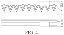
- FIG. 4 is a schematic structural diagram of a fourth solar cell according to an embodiment of this application. Referring to FIG. 1 to FIG. 4 , the embodiments of this application provide a solar cell, including: a silicon substrate 1, and a low-absorption coefficient layer 2 arranged on a light-receiving surface of the silicon substrate.
- ⁇ a is the absorption coefficient
- ⁇ is an extinction coefficient
- ⁇ is a wavelength.
- the extinction coefficient ⁇ is greater than 2.9 in a wavelength band of 200 to 350 nm, and is less than 2.9 only in a wavelength band of 350 to 400 nm, but sharply increases as the wavelength decreases.
- ⁇ 0.0122 nm -1 .
- a thickness of 10 nm is required, so that most of incident light in the wavelength band of 350 nm can be absorbed.
- the silicon material For incident light in the wavelength band of 200 to 350 nm, the silicon material only needs to have a thickness of less than 10 nm, to achieve absorption of most of the incident light.
- a yield of non-equilibrium carriers in the light-receiving surface of the silicon substrate is G ⁇ ⁇ f ⁇ ⁇ ⁇ e - ⁇ x dx, where the absorption coefficient ⁇ is directly proportional to G, and the two have direct impact.
- G may also decrease by an order of magnitude.
- the light-receiving surface of the silicon substrate 1 has a large absorption coefficient for the short-wavelength band of less than or equal to 400 nm, the light-receiving surface of the silicon substrate 1 has a high concentration of non-equilibrium carriers.
- the non-equilibrium minority carriers in the light-receiving surface of the silicon substrate 1 can be effectively conducted and collected, to facilitate reduction of the concentration of the non-equilibrium carriers in the light-receiving surface of the silicon substrate 1, and facilitate reduction of recombination of the light-receiving surface of the silicon substrate 1.
- the thickness x of the low-absorption coefficient layer 2 may be 15 nm, 30 nm, 50 nm, 90 nm, 110 nm, 130 nm, 170 nm, or 200 nm.
- a direction of the thickness is parallel to the direction in which the silicon substrate 1 and the low-absorption coefficient layer 2 are arranged, and directions of thicknesses in this specification each is defined as the same.
- the low-absorption coefficient layer 2 is in direct contact with the silicon substrate 1, and a status of an interface between the two is not specifically limited.
- the interface between the two may be an epitaxial interface or a chemical bond interface.
- the epitaxial interface is a lattice-matched interface, and there is almost no interface through a high-precision transmission electron microscope.
- the low-absorption coefficient layer 2 and the silicon substrate 1 may be considered as a whole.
- the chemical bond interface may be an interface on which the low-absorption coefficient layer 2 and the silicon substrate 1 are bonded. On the interface, lattices in some regions may be matched, and lattice in the other regions are mismatched.
- the low-absorption coefficient layer 2 may be made of a polycrystalline material or a monocrystalline material, which is not specifically limited.
- the low-absorption coefficient layer 2 may be made of the monocrystalline material, so that an interface with excellent performance can be formed between the low-absorption coefficient layer 2 and the silicon substrate 1.
- a band gap of the low-absorption coefficient layer 2 is greater than or equal to a band gap of the silicon substrate 1, which can ensure that the silicon substrate 1 is a main absorbing material for light in a wavelength band of greater than 400 nm.
- the silicon substrate 1 has a large absorption coefficient in the wavelength band of less than or equal to 400 nm, the light-receiving surface of the silicon substrate 1 has a high concentration of non-equilibrium carriers.
- the silicon substrate 1 absorbs less light in the wavelength band of less than or equal to 400 nm, to reduce the concentration of the non-equilibrium carriers in the light-receiving surface of the silicon substrate 1.
- as much light as possible in the wavelength band of greater than 400 nm is absorbed by the silicon substrate 1.
- the thickness x of the low-absorption coefficient layer 2 ranges from 20 to 100 nm.
- the thickness of the low-absorption coefficient layer 2 is suitable, so that the light in the wavelength band of less than or equal to 400 nm can be fully absorbed, and the concentration of the minority carriers in the low-absorption coefficient layer 2 is not excessively low, so that the minority carriers in the silicon substrate 1 are not injected into the low-absorption coefficient layer 2, to facilitate transport of the non-equilibrium minority carriers in the light-receiving surface of the silicon substrate 1.
- the non-equilibrium minority carriers in the light-receiving surface of the silicon substrate 1 can be effectively conducted and collected, to facilitate reduction of the concentration of the non-equilibrium carriers in the light-receiving surface of the silicon substrate 1, and facilitate reduction of recombination of the light-receiving surface of the silicon substrate 1.
- the thickness x of the low-absorption coefficient layer 2 may be 20 nm, 30 nm, 42 nm, 55 nm, 63 nm, 77 nm, 89 nm, or 100 nm.
- the thickness x of the low-absorption coefficient layer 2 is suitable, so that the light in the wavelength band of less than or equal to 400 nm can be fully absorbed, and the concentration of the minority carriers in the low-absorption coefficient layer 2 is not excessively low, so that the minority carriers in the silicon substrate 1 are not injected into the low-absorption coefficient layer 2, to facilitate transport of the non-equilibrium minority carriers in the light-receiving surface of the silicon substrate 1.
- an extinction coefficient of the low-absorption coefficient layer 2 is greater than or equal to 0.1 and less than or equal to 2.
- the extinction coefficient of the low-absorption coefficient layer 2 is directly proportional to the absorption coefficient of the low-absorption coefficient layer 2.
- the absorption coefficient of the low-absorption coefficient layer 2 is suitable, which is suitable for the amount of light absorbed by the low-absorption coefficient layer 2 in the wavelength band of 300 to 400 nm, and suitable for the amount of light absorbed by the silicon substrate 1 in the wavelength band of 300 to 400 nm, so that the concentration of the non-equilibrium carriers in the light-receiving surface of the silicon substrate 1 can be reduced.
- the extinction coefficient of the low-absorption coefficient layer 2 is 0.1, 0.3, 0.5, 0.8, 0.9, 1.1, 1.5, 1.9, or 2.
- an integral average extinction coefficient of the low-absorption coefficient layer 2 is greater than or equal to 0.1 and less than or equal to 2.
- the integral average extinction coefficient is obtained in the following manner: By using a wavelength band of 300 to 400 nm as an integral interval and using the extinction coefficient of the low-absorption coefficient layer 2 as an integrated function, integration is performed, and then an integration result is divided by a length of the integral interval.
- the absorption coefficient of the low-absorption coefficient layer 2 is suitable, which is suitable for the amount of light absorbed by the low-absorption coefficient layer 2 in the wavelength band of 300 to 400 nm, and suitable for the amount of light absorbed by the silicon substrate 1 in the wavelength band of 300 to 400 nm, so that the concentration of the non-equilibrium carriers in the light-receiving surface of the silicon substrate 1 can be reduced.
- the integral average extinction coefficient of the low-absorption coefficient layer 2 is 0.1, 0.3, 0.46, 0.73, 0.92, 1.1, 1.5, 1.88, or 2.
- a material of the low-absorption coefficient layer 2 is selected from at least one of boron carbide, zinc oxide, gallium phosphide, indium phosphide, cadmium sulfide, zinc sulfide, arsenic selenide, cadmium selenide, or zinc selenide.
- the low-absorption coefficient layer 2 of the foregoing material has a suitable absorption coefficient in the wavelength band of 300 to 400 nm, so that the concentration of the non-equilibrium carriers in the light-receiving surface of the silicon substrate 1 can be reduced.
- lattice constants of the low-absorption coefficient layer 2 of the foregoing material and the silicon substrate 1 are relatively close, and an epitaxial interface or a chemical bond interface is prone to be formed between the two, to facilitate conduction or transport of carriers on the interface between the two, thereby improving the photoelectric conversion efficiency of the solar cell.
- a lattice constant of silicon in the silicon substrate 1 is 5.43 ⁇ (angstroms).
- a lattice constant of boron carbide is 5.19 ⁇ , and in the wavelength band of 300 to 400 nm, an extinction coefficient of boron carbide roughly ranges from 1.05 to 0.76. If boron carbide is used as the material of the low-absorption coefficient layer 2, the concentration of the non-equilibrium carriers in the light-receiving surface of the silicon substrate 1 can be reduced.
- the lattice constants of the low-absorption coefficient layer 2 of the boron carbide material and the silicon substrate 1 are relatively close, and the epitaxial interface or the chemical bond interface is prone to be formed between the two, to facilitate conduction or transport of the carriers on the interface between the two, thereby improving the photoelectric conversion efficiency of the solar cell.
- a lattice constant of zinc oxide is 5.2 ⁇ , and in the wavelength band of 300 to 400 nm, an extinction coefficient of zinc oxide roughly ranges from 0.196 to 0.254 and from 0.254 to 0.109.
- a lattice constant of gallium phosphide is 5.44 ⁇ , and in the wavelength band of 300 to 400 nm, an extinction coefficient of gallium phosphide roughly ranges from 2.1 to 0.275.
- a lattice constant of indium phosphide is 5.87 ⁇ , and in the wavelength band of 300 to 400 nm, an extinction coefficient of indium phosphide roughly ranges from 1.7 to 2.2 and from 2.2 to 1.7.
- a lattice constant of cadmium sulfide is 5.86 ⁇ , and in the wavelength band of 300 to 400 nm, an extinction coefficient of cadmium sulfide roughly ranges from 0.39 to 0.34.
- a lattice constant of zinc sulfide is 5.47 ⁇ , and in the wavelength band of 300 to 400 nm, an extinction coefficient of zinc sulfide roughly ranges from 0.357 to 0.008.
- a lattice constant of arsenic selenide is 4.51 ⁇ , and in the wavelength band of 300 to 400 nm, an extinction coefficient of arsenic selenide roughly ranges from 1.66 to 1.86 and from 1.86 to 1.65.
- a lattice constant of cadmium selenide is 5.86 ⁇ , and in the wavelength band of 300 to 400 nm, an extinction coefficient of cadmium selenide roughly ranges from 1.34 to 0.56.
- a lattice constant of zinc selenide is 5.66 ⁇ , and in the wavelength band of 300 to 400 nm, an extinction coefficient of zinc selenide roughly ranges from 0.79 to 0.48.
- the material of the low-absorption coefficient layer 2 is selected from zinc oxide; and the solar cell further includes: a front anti-reflection layer 313 and a front electrode 32 located on a side of the low-absorption coefficient layer 2 away from the silicon substrate 1, where the front electrode 32 penetrates the front anti-reflection layer 313 to come into contact with the low-absorption coefficient layer 2.
- the material of the low-absorption coefficient layer 2 is selected from zinc oxide.
- the low-absorption coefficient layer 2 has at least two roles: One is a low-absorption coefficient role in the wavelength band of 300 to 400 nm, and the other is a front carrier transport role or a front selective contact role.
- the low-absorption coefficient layer 2 of the zinc oxide material is doped is not specifically limited.
- the low-absorption coefficient layer 2 of the zinc oxide material may not be doped, and a type of the silicon substrate 1 is also the N-type conductivity type.
- an entire region or a local region of the low-absorption coefficient layer 2 of the zinc oxide material has surface doping, so that the conductivity type of the low-absorption coefficient layer 2 of the zinc oxide material can be improved.
- an element such as aluminum, indium, or gallium may be doped in the low-absorption coefficient layer 2 of the zinc oxide material.
- a doping concentration and the like of the low-absorption coefficient layer 2 are not specifically limited.
- the thickness of the low-absorption coefficient layer 2 of the zinc oxide material may range from 15 to 100 nm.
- the low-absorption coefficient layer 2 of the zinc oxide material in the foregoing thickness range has a good low-absorption coefficient role, and a good front carrier transport role or front selective contact role in the wavelength band of 300 to 400 nm.
- the thickness of the low-absorption coefficient layer 2 of the zinc oxide material may be 15 nm, 23 nm, 36 nm, 45 nm, 58 nm, 66 nm, 79 nm, 88 nm, or 100 nm.
- the thickness of the low-absorption coefficient layer 2 of the zinc oxide material may further range from 20 to 50 nm.
- the low-absorption coefficient layer 2 of the zinc oxide material in the foregoing thickness range has a better low-absorption coefficient role, and a better front carrier transport role or front selective contact role in the wavelength band of 300 to 400 nm.
- the thickness of the low-absorption coefficient layer 2 of the zinc oxide material may be 20 nm, 23 nm, 29 nm, 36 nm, 38 nm, 42 nm, 47 nm, or 50 nm.
- a material, a structure, a thickness, and the like of the front anti-reflection layer 313 are all not specifically limited.
- the material of the front anti-reflection layer 313 may be selected from at least one of silicon nitride, magnesium fluoride, silicon oxide, zinc sulfide, silicon oxynitride, aluminum nitride, titanium nitride, aluminum oxide, or titanium oxide.
- the front anti-reflection layer 313 may be a laminated-layer structure of an aluminum nitride layer and a titanium nitride layer.
- This application further provides a method for preparing the solar cell according to any one of the foregoing descriptions, including the following steps: arranging a low-absorption coefficient layer on a light-receiving surface of a silicon substrate, where the low-absorption coefficient layer and the light-receiving surface of the silicon substrate have a same conductivity type; in a wavelength band of less than or equal to 400 nm, an absorption coefficient of the low-absorption coefficient layer is less than an absorption coefficient of the silicon substrate; a thickness x of the low-absorption coefficient layer ranges from 15 to 200 nm, and a direction of the thickness is parallel to a direction in which the silicon substrate and the low-absorption coefficient layer are arranged; and the low-absorption coefficient layer is in direct contact with the silicon substrate.
- the preparation method can achieve the same or similar beneficial effects as the solar cell according to any one of the foregoing descriptions. To avoid repetition, details are not described in relevant parts.
- the foregoing solar cell, the photovoltaic module, and the method for preparing the solar cell may be referred to each other, and can achieve the same or similar beneficial effects. To avoid repetition, details are not described in relevant parts.
- An n-type silicon wafer is used as a silicon substrate 1.
- the thickness and the doping concentration of the silicon substrate are not limited.
- the silicon substrate 1 has a doping concentration ranging from 10 10 /cm 3 to 10 16 /cm 3 , and a thickness that may range from 30 to 150 ⁇ m (micron), or from 50 to 200 ⁇ m.
- the silicon substrate 1 with a low doping concentration of 10 10 /cm 3 to 10 14 /cm 3 may have a large thickness, which may range from 80 to 150 ⁇ m.
- the silicon substrate 1 with a high doping concentration of 10 14 /cm 3 to 10 16 /cm 3 may have a small thickness, which may range from 30 to 80 ⁇ m.
- a light-receiving surface of the silicon substrate 1 may be a planar structure or a low-roughness light-trapping structure, and a back surface of the silicon substrate 1 has a textured light-trapping structure.
- a low-absorption coefficient layer 2 is arranged on the light-receiving surface of the silicon substrate 1.
- the low-absorption coefficient layer 2 is made of a material including gallium phosphide (GaP) or indium phosphide (InP), has a thickness of 20 to 100 nm, for example, 20 to 50 nm, and has an n-type conductivity type.
- the low-absorption coefficient layer 2 is prepared by using a chemical vapor epitaxy deposition method, for example, a chemical molecular beam epitaxy process or an atomic layer deposition process.
- a front passivated contact layer 312 is arranged on a light-receiving surface of the low-absorption coefficient layer 2.
- the front passivated contact layer 312 is made of a material including wide-band gap group III-V materials, for example, AlGaAs, AlGaInP, or GaInAs (where the stoichiometric ratio is not limited).
- a front anti-reflection layer 313 is arranged on a light-receiving surface of the front passivated contact layer 312.
- a material of the front anti-reflection layer 313 includes silicon nitride, magnesium fluoride, silicon oxide, or the like.
- a front electrode 32 penetrates the front anti-reflection layer 313 to come into electrical contact with the front passivated contact layer 312, or to come into partial contact with the low-absorption coefficient layer 2.
- the front electrode 32 is a single-layer or laminated-layer structure formed by at least one of silver, copper, nickel, zinc, or aluminum.
- the back surface of the solar cell is a conventional TOPCon structure having a back passivation layer 411.
- a material of the back passivation layer 411 is silicon oxide.
- the back transport layer 412 is made of doped polysilicon.
- a doping type of the back transport layer 412 is the same as that of the back surface of the silicon substrate 1. If the low-absorption coefficient layer 2 is made of an n-type material, the back surface of the silicon substrate 1 is a p-type diffusion or injection layer, and the back transport layer 412 is made of p-type polysilicon.
- the back surface of the silicon substrate 1 may be a non-diffused or diffused or ion-injected n-type heavily doped layer, and the back transport layer 412 is made of n-type polysilicon.
- a back anti-reflection layer 413 is arranged on a back surface of the back transport layer 412, and is made of at least one of silicon nitride, magnesium fluoride, or silicon oxide.
- a back electrode 42 penetrates the back anti-reflection layer 413 to come into electrical contact with the back transport layer 412, or partially penetrates the back transport layer 412 and the back passivation layer 411 to come into contact with the back surface of the silicon substrate 1.
- a material of the back electrode 42 is selected from at least one of silver, copper, nickel, zinc, or aluminum, to form a single-layer structure or a laminated-layer structure.
- an n-type silicon wafer is used as a silicon substrate 1.
- the thickness and the doping concentration of the silicon substrate are not limited.
- the silicon substrate 1 has a doping concentration ranging from 10 10 /cm 3 to 10 16 /cm 3 , and a thickness ranging from 30 to 150 ⁇ m.
- the silicon substrate 1 with a low doping concentration of 10 10 /cm 3 to 10 14 /cm 3 may have a large thickness, which may range from 80 to 150 ⁇ m.
- the silicon substrate 1 with a high doping concentration of 10 14 /cm 3 to 10 16 /cm 3 may have a small thickness, which may range from 30 to 80 ⁇ m.
- a light-receiving surface of the silicon substrate 1 may be a planar structure or a low-roughness light-trapping structure, and a back surface of the silicon substrate 1 has a textured light-trapping structure.
- a low-absorption coefficient layer 2 is arranged on the light-receiving surface of the silicon substrate 1.
- the low-absorption coefficient layer 2 is made of a material including zinc oxide, and has a thickness of 15 to 100 nm, for example, 20 to 50 nm.
- Zinc oxide naturally has an n-type conductivity type. Doping may be performed on zinc oxide to improve the conductivity or enhance the conductivity type.
- an element such as aluminum, indium, or gallium may be doped in zinc oxide.
- the low-absorption coefficient layer 2 may be prepared by using a process such as chemical vapor deposition, evaporative deposition, or molecular beam epitaxy.
- a buffer layer may exist between the low-absorption coefficient layer 2 and the silicon substrate 1.
- a material of the buffer layer may be selected as, for example, silicon oxide, zinc sulfide, silicon carbide, aluminum nitride, or silicon nitride.
- a thickness of the buffer layer does not exceed 4 nm.
- the thickness of the buffer layer does not exceed 2 nm.
- a front anti-reflection layer 313 is arranged on a light-receiving surface of the low-absorption coefficient layer 2, and is made of at least one of silicon nitride, magnesium fluoride, silicon oxide, or zinc sulfide.
- a front electrode 32 penetrates the front anti-reflection layer 313 to come into electrical contact with the low-absorption coefficient layer 2.
- a material of the front electrode 32 is selected from at least one of silver, copper, nickel, zinc, or aluminum, to form a single-layer structure or a laminated-layer structure.
- a back surface of a solar cell is a conventional Hetero-junction with intrinsic thin-layer (HJT) structure.
- a back passivation layer 411 is arranged on the back surface of the silicon substrate 1, and is made of intrinsic amorphous silicon.
- a back transport layer 412 is arranged on a surface of the back passivation layer 411.
- the back transport layer 412 is a multilayer structure of p-type amorphous silicon or nanocrystalline silicon, and a transparent conductive thin film.
- a back anti-reflection layer 413 is arranged on a back surface of the back transport layer 412, and is made of silicon nitride; silicon nitride and magnesium fluoride; silicon oxide, silicon nitride, and magnesium fluoride; or the like.
- a back electrode 42 penetrates the back anti-reflection layer 413 to come into electrical contact with the back transport layer 412.
- a material of the back electrode 42 is selected from at least one of silver, copper, nickel, zinc, or aluminum, to form a single-layer structure or a laminated-layer structure.
- a back surface of a solar cell is a dopant-free asymmetric heterocontact (DASH) structure.
- An n-type silicon wafer is used as a silicon substrate 1.
- the silicon substrate 1 has a doping concentration ranging from 10 10 /cm 3 to 10 16 /cm 3 , and a thickness ranging from 30 to 150 ⁇ m.
- the silicon substrate 1 with a low doping concentration of 10 10 /cm 3 to 10 14 /cm 3 may have a large thickness, which may range from 80 to 150 ⁇ m.
- the silicon substrate 1 with a high doping concentration of 10 14 /cm 3 to 10 16 /cm 3 may have a small thickness, which may range from 30 to 80 ⁇ m.
- a light-receiving surface of the silicon substrate 1 may be a planar structure or a low-roughness light-trapping structure, and a back surface of the silicon substrate 1 has a textured light-trapping structure.
- a low-absorption coefficient layer 2 is arranged on the light-receiving surface of the silicon substrate 1.
- the low-absorption coefficient layer 2 is made of a material including zinc sulfide or zinc selenide, and has a thickness of 15 to 100 nm, for example, 20 to 50 nm.
- the low-absorption coefficient layer 2 has an n-type conductivity type. Doping may be performed on zinc sulfide or zinc selenide to improve the conductivity or enhance the conductivity type. For example, an element such as aluminum, indium, or gallium may be doped in zinc sulfide or zinc selenide.
- the low-absorption coefficient layer 2 is prepared by using a process such as chemical vapor deposition, evaporative deposition, or molecular beam epitaxy. Alternatively, the low-absorption coefficient layer 2 may be made of a material including zinc oxide or another foregoing material.
- a front passivated contact layer 312 is arranged on the low-absorption coefficient layer 2, and is a transparent conductive thin film, for example, zinc oxide (in which aluminum, indium, or gallium may be doped) or indium tin oxide.
- a front anti-reflection layer 313 is arranged on the front passivated contact layer 312, and is made of silicon nitride; silicon nitride and magnesium fluoride; silicon oxide, silicon nitride, and magnesium fluoride; or the like.
- a front electrode 32 penetrates the front anti-reflection layer 313 to come into electrical contact with the front passivated contact layer 312, or to come into partial contact with the low-absorption coefficient layer 2.
- the front electrode 32 is a single-layer or laminated-layer structure formed by at least one of silver, copper, nickel, zinc, or aluminum.
- the back surface of the solar cell is the DASH structure.
- a back passivation layer 411 is arranged on the back surface of the silicon substrate 1, and is made of silicon oxide.
- a back transport layer 412 is arranged on a surface of the back passivation layer 411, and is made of a laminated material of a wide-band gap transition metal oxide and a transparent conductive thin film.
- the wide-band gap transition metal oxide has a conductivity type opposite to that of the low-absorption coefficient layer 2.
- a p-type material can be selected to have a high work function.
- the p-type material is, for example, molybdenum oxide, tungsten oxide, or vanadium oxide.
- the p-type material may alternatively be selected as a p-type oxide, for example, nickel oxide.
- An n-type material may be selected as an n-type oxide, for example, zinc oxide, tin oxide, or titanium oxide.
- a back anti-reflection layer 413 is arranged on a back surface of the back transport layer 412, and is made of silicon nitride; silicon nitride and magnesium fluoride; silicon oxide, silicon nitride, and magnesium fluoride; or the like.
Landscapes
- Photovoltaic Devices (AREA)
Abstract
Description
- This application claims priority to
Chinese Patent Application No. 202210738973.X, filed with the China National Intellectual Property Administration on June 27, 2022 - This application relates to the field of photovoltaic technologies, and in particular, to a solar cell, a preparation method therefor, and a photovoltaic module.
- Solar cells are power generation devices that directly converts sunlight into electrical energy output. As a clean energy source, solar cells have broad application prospects.
- Currently, solar cells have a problem of poor short-wavelength response. The poor short-wavelength response leads to a decrease in photoelectric conversion efficiency of the solar cells.
- This application provides a solar cell, a preparation method therefor, and a photovoltaic module, to resolve a problem that a solar cell has a poor short-wavelength response.
- According to a first aspect of this application, a solar cell is provided, including:
- a silicon substrate, and a low-absorption coefficient layer arranged on a light-receiving surface of the silicon substrate, where
- the low-absorption coefficient layer and the light-receiving surface of the silicon substrate have a same conductivity type;
- in a wavelength band of less than or equal to 400 nm, an absorption coefficient of the low-absorption coefficient layer is less than an absorption coefficient of the silicon substrate;
- a thickness x of the low-absorption coefficient layer ranges from 15 to 200 nm, and a direction of the thickness is parallel to a direction in which the silicon substrate and the low-absorption coefficient layer are arranged; and
- the low-absorption coefficient layer is in direct contact with the silicon substrate.
- In embodiments of this application, a low-absorption coefficient layer and a light-receiving surface of a silicon substrate have a same conductivity type, to facilitate transport of minority carriers. In this way, non-equilibrium minority carriers in the light-receiving surface of the silicon substrate can be effectively conducted and collected, to facilitate reduction of a concentration of non-equilibrium carriers in the light-receiving surface of the silicon substrate, and facilitate reduction of recombination of the light-receiving surface of the silicon substrate, so that photoelectric conversion efficiency of a solar cell can be improved. The low-absorption coefficient layer is in direct contact with the silicon substrate, and in a wavelength band of less than or equal to 400 nm, an absorption coefficient of the low-absorption coefficient layer is less than an absorption coefficient of the silicon substrate. The low-absorption coefficient layer absorbs a part of light in the wavelength band of less than or equal to 400 nm, so that light absorbed by the silicon substrate in the wavelength band of less than or equal to 400 nm is reduced. In this way, the concentration of the non-equilibrium carriers in the light-receiving surface of the silicon substrate can be reduced, and the recombination of the light-receiving surface of the silicon substrate can be reduced. In addition, a thickness x of the low-absorption coefficient layer ranges from 15 to 200 nm. The low-absorption coefficient layer is not excessively thin, so that the light in the wavelength band of less than or equal to 400 nm can be fully absorbed; and the low-absorption coefficient layer is not excessively thick, and a concentration of minority carriers in the low-absorption coefficient layer is not excessively low, so that minority carriers in the silicon substrate are not injected into the low-absorption coefficient layer, to facilitate transport of the non-equilibrium minority carriers in the light-receiving surface of the silicon substrate. In this way, the non-equilibrium minority carriers in the light-receiving surface of the silicon substrate can be effectively conducted and collected, to facilitate reduction of the concentration of the non-equilibrium carriers in the light-receiving surface of the silicon substrate, and facilitate reduction of recombination of the light-receiving surface of the silicon substrate, so that the photoelectric conversion efficiency of the solar cell can be improved.
- Optionally, a band gap of the low-absorption coefficient layer is greater than or equal to a band gap of the silicon substrate.
- Optionally, the thickness x of the low-absorption coefficient layer ranges from 20 to 100 nm.
- Optionally, the thickness of the low-absorption coefficient layer is

- Optionally, in a wavelength band of 300 to 400 nm, an extinction coefficient of the low-absorption coefficient layer is greater than or equal to 0.1 and less than or equal to 2.
- Optionally, in a wavelength band of 300 to 400 nm, an integral average extinction coefficient of the low-absorption coefficient layer is greater than or equal to 0.1 and less than or equal to 2.
- Optionally, a material of the low-absorption coefficient layer is selected from at least one of boron carbide, zinc oxide, gallium phosphide, indium phosphide, cadmium sulfide, zinc sulfide, arsenic selenide, cadmium selenide, or zinc selenide.
- Optionally, the material of the low-absorption coefficient layer is selected from zinc oxide; and the solar cell further includes: a front anti-reflection layer and a front electrode located on a side of the low-absorption coefficient layer away from the silicon substrate, where the front electrode penetrates the front anti-reflection layer to come into contact with the low-absorption coefficient layer.
- Optionally, the low-absorption coefficient layer has a locally doped region, and the locally doped region is a front selective contact region; or the low-absorption coefficient layer is an entirely doped layer, and the low-absorption coefficient layer is a front selective contact layer; and
the solar cell further includes: a front electrode located on a side of the low-absorption coefficient layer away from the silicon substrate, where the front electrode is in contact with the front selective contact region or the front selective contact layer. - Optionally, the solar cell further includes: a buffer layer located between the silicon substrate and the low-absorption coefficient layer, where a material of the buffer layer is selected from at least one of silicon oxide, zinc sulfide, silicon carbide, aluminum nitride, or silicon nitride.
- Optionally, a thickness of the buffer layer is less than or equal to 4 mm, and a direction of the thickness of the buffer layer is parallel to the direction in which the silicon substrate and the low-absorption coefficient layer are arranged.
- Optionally, the light-receiving surface of the silicon substrate has a light-trapping structure.
- According to a second aspect of this application, a photovoltaic module is provided, including a plurality of solar cells according to any one of the foregoing descriptions.
- According to a third aspect of this application, a method for preparing the solar cell according to any one of the foregoing descriptions is provided, including: arranging a low-absorption coefficient layer on a light-receiving surface of a silicon substrate, where the low-absorption coefficient layer and the light-receiving surface of the silicon substrate have a same conductivity type; in a wavelength band of less than or equal to 400 nm, an absorption coefficient of the low-absorption coefficient layer is less than an absorption coefficient of the silicon substrate; a thickness x of the low-absorption coefficient layer ranges from 15 to 200 nm, and a direction of the thickness is parallel to a direction in which the silicon substrate and the low-absorption coefficient layer are arranged; and the low-absorption coefficient layer is in direct contact with the silicon substrate.
- Optionally, the arranging a low-absorption coefficient layer on a light-receiving surface of a silicon substrate includes:
arranging the low-absorption coefficient layer on the light-receiving surface of the silicon substrate through chemical vapor deposition, evaporation deposition, or molecular beam epitaxy. - To describe the technical solutions in embodiments of this application more clearly, the following briefly describes the accompanying drawings required for describing the embodiments of this application. Apparently, the accompanying drawings in the following description show merely some embodiments of this application, and a person of ordinary skill in the art may still derive other accompanying drawings from these accompanying drawings without creative efforts.
-
FIG. 1 is a schematic structural diagram of a first solar cell according to an embodiment of this application; -
FIG. 2 is a schematic structural diagram of a second solar cell according to an embodiment of this application; -
FIG. 3 is a schematic structural diagram of a third solar cell according to an embodiment of this application; and -
FIG. 4 is a schematic structural diagram of a fourth solar cell according to an embodiment of this application. - Descriptions of reference numerals:
1-silicon substrate, 2-low-absorption coefficient layer, 31-front functional layer, 312-front passivated contact layer, 313-front anti-reflection layer, 32-front electrode, 41-back functional layer, 411-back passivation layer, 412-back transport layer, 413-back anti-reflection layer, and 42-back electrode. - The following clearly and completely describes the technical solutions in the embodiments of this application with reference to the accompanying drawings in the embodiments of this application. Apparently, the described embodiments are some embodiments of this application rather than all of the embodiments. All other embodiments obtained by a person of ordinary skill in the art based on the embodiments of this application without creative efforts shall fall within the protection scope of this application.
-
FIG. 1 is a schematic structural diagram of a first solar cell according to an embodiment of this application.FIG. 2 is a schematic structural diagram of a second solar cell according to an embodiment of this application.FIG. 3 is a schematic structural diagram of a third solar cell according to an embodiment of this application.FIG. 4 is a schematic structural diagram of a fourth solar cell according to an embodiment of this application. Referring toFIG. 1 to FIG. 4 , the embodiments of this application provide a solar cell, including: asilicon substrate 1, and a low-absorption coefficient layer 2 arranged on a light-receiving surface of the silicon substrate. - Specifically, the applicant has found that, in existing technologies, a reason for a poor short-wavelength response of a solar cell is that: The light-receiving surface of the
silicon substrate 1 has a large absorption coefficient for a short-wavelength band of less than or equal to 400 nm (nanometers). As a result, most of incident light is absorbed through a shallow depth of the light-receiving surface of thesilicon substrate 1. For example, through a thickness of 10 nm from the light-receiving surface of the silicon substrate to the inside of thesilicon substrate 1, the incident light in the wavelength band of less than or equal to 400 nm can be completely absorbed. In this way, under illumination, there is a high concentration of non-equilibrium carriers, and the non-equilibrium carriers of the high concentration cannot be effectively conducted and collected in time, resulting in severe recombination of the light-receiving surface of thesilicon substrate 1. - More specifically, an absorption coefficient of a material is directly associated with optical parameters of the material, which is shown in, for example, the following formula:

silicon substrate 1 has a large absorption coefficient for the short-wavelength band of less than or equal to 400 nm, the light-receiving surface of thesilicon substrate 1 has a high concentration of non-equilibrium carriers. - For the foregoing problems, in this application, a low-
absorption coefficient layer 2 and a light-receiving surface of asilicon substrate 1 have a same conductivity type, to facilitate transport of minority carriers. In this way, non-equilibrium minority carriers in the light-receiving surface of thesilicon substrate 1 can be effectively conducted and collected, to facilitate reduction of a concentration of non-equilibrium carriers in the light-receiving surface of thesilicon substrate 1, and facilitate reduction of recombination of the light-receiving surface of thesilicon substrate 1, so that photoelectric conversion efficiency of a solar cell can be improved. The low-absorption coefficient layer 2 is in direct contact with thesilicon substrate 1, and in a wavelength band of less than or equal to 400 nm, an absorption coefficient of the low-absorption coefficient layer 2 is less than an absorption coefficient of thesilicon substrate 1. The low-absorption coefficient layer 2 absorbs a part of light in the wavelength band of less than or equal to 400 nm, so that light absorbed by thesilicon substrate 1 in the wavelength band of less than or equal to 400 nm is reduced. In this way, the concentration of the non-equilibrium carriers in the light-receiving surface of thesilicon substrate 1 can be reduced, and the recombination of the light-receiving surface of thesilicon substrate 1 can be reduced, so that the photoelectric conversion efficiency of the solar cell can be improved. In addition, a thickness x of the low-absorption coefficient layer 2 ranges from 15 to 200 nm. The low-absorption coefficient layer 2 is not excessively thin, so that the light in the wavelength band of less than or equal to 400 nm can be fully absorbed; and the low-absorption coefficient layer 2 is not excessively thick, and a concentration of minority carriers in the low-absorption coefficient layer 2 is not excessively low, so that minority carriers in thesilicon substrate 1 are not injected into the low-absorption coefficient layer 2, to facilitate transport of the non-equilibrium minority carriers in the light-receiving surface of thesilicon substrate 1. In this way, the non-equilibrium minority carriers in the light-receiving surface of thesilicon substrate 1 can be effectively conducted and collected, to facilitate reduction of the concentration of the non-equilibrium carriers in the light-receiving surface of thesilicon substrate 1, and facilitate reduction of recombination of the light-receiving surface of thesilicon substrate 1. - For example, the thickness x of the low-
absorption coefficient layer 2 may be 15 nm, 30 nm, 50 nm, 90 nm, 110 nm, 130 nm, 170 nm, or 200 nm. A direction of the thickness is parallel to the direction in which thesilicon substrate 1 and the low-absorption coefficient layer 2 are arranged, and directions of thicknesses in this specification each is defined as the same. - The low-
absorption coefficient layer 2 is in direct contact with thesilicon substrate 1, and a status of an interface between the two is not specifically limited. For example, the interface between the two may be an epitaxial interface or a chemical bond interface. The epitaxial interface is a lattice-matched interface, and there is almost no interface through a high-precision transmission electron microscope. The low-absorption coefficient layer 2 and thesilicon substrate 1 may be considered as a whole. The chemical bond interface may be an interface on which the low-absorption coefficient layer 2 and thesilicon substrate 1 are bonded. On the interface, lattices in some regions may be matched, and lattice in the other regions are mismatched. Through a transmission electron microscope, there is a display interface between the low-absorption coefficient layer 2 and thesilicon substrate 1. It should be noted that, on the interface between the low-absorption coefficient layer 2 and thesilicon substrate 1, a larger region in which lattices are matched indicates that it is more conducive to conduction or transport of carriers on the interface between the two. A doping concentration, a doping type, a thickness, and the like of thesilicon substrate 1 are all not limited in this application. - The low-
absorption coefficient layer 2 may be made of a polycrystalline material or a monocrystalline material, which is not specifically limited. For example, the low-absorption coefficient layer 2 may be made of the monocrystalline material, so that an interface with excellent performance can be formed between the low-absorption coefficient layer 2 and thesilicon substrate 1. - Optionally, a band gap of the low-
absorption coefficient layer 2 is greater than or equal to a band gap of thesilicon substrate 1, which can ensure that thesilicon substrate 1 is a main absorbing material for light in a wavelength band of greater than 400 nm. In other words, because thesilicon substrate 1 has a large absorption coefficient in the wavelength band of less than or equal to 400 nm, the light-receiving surface of thesilicon substrate 1 has a high concentration of non-equilibrium carriers. In this application, thesilicon substrate 1 absorbs less light in the wavelength band of less than or equal to 400 nm, to reduce the concentration of the non-equilibrium carriers in the light-receiving surface of thesilicon substrate 1. In addition, as much light as possible in the wavelength band of greater than 400 nm is absorbed by thesilicon substrate 1. - Optionally, the thickness x of the low-
absorption coefficient layer 2 ranges from 20 to 100 nm. In this case, the thickness of the low-absorption coefficient layer 2 is suitable, so that the light in the wavelength band of less than or equal to 400 nm can be fully absorbed, and the concentration of the minority carriers in the low-absorption coefficient layer 2 is not excessively low, so that the minority carriers in thesilicon substrate 1 are not injected into the low-absorption coefficient layer 2, to facilitate transport of the non-equilibrium minority carriers in the light-receiving surface of thesilicon substrate 1. In this way, the non-equilibrium minority carriers in the light-receiving surface of thesilicon substrate 1 can be effectively conducted and collected, to facilitate reduction of the concentration of the non-equilibrium carriers in the light-receiving surface of thesilicon substrate 1, and facilitate reduction of recombination of the light-receiving surface of thesilicon substrate 1. - For example, the thickness x of the low-
absorption coefficient layer 2 may be 20 nm, 30 nm, 42 nm, 55 nm, 63 nm, 77 nm, 89 nm, or 100 nm. - Optionally, the thickness of the low-
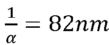
absorption coefficient layer 2 is
absorption coefficient layer 2 in a wavelength band of 200 to 400 nm. In this case, the thickness x of the low-absorption coefficient layer 2 is suitable, so that the light in the wavelength band of less than or equal to 400 nm can be fully absorbed, and the concentration of the minority carriers in the low-absorption coefficient layer 2 is not excessively low, so that the minority carriers in thesilicon substrate 1 are not injected into the low-absorption coefficient layer 2, to facilitate transport of the non-equilibrium minority carriers in the light-receiving surface of thesilicon substrate 1. In this way, the non-equilibrium minority carriers in the light-receiving surface of thesilicon substrate 1 can be effectively conducted and collected, to facilitate reduction of the concentration of the non-equilibrium carriers in the light-receiving surface of thesilicon substrate 1, and facilitate reduction of recombination of the light-receiving surface of thesilicon substrate 1. - Optionally, in a wavelength band of 300 to 400 nm, an extinction coefficient of the low-
absorption coefficient layer 2 is greater than or equal to 0.1 and less than or equal to 2. The extinction coefficient of the low-absorption coefficient layer 2 is directly proportional to the absorption coefficient of the low-absorption coefficient layer 2. If the extinction coefficient of the low-absorption coefficient layer 2 is in the wavelength band of 300 to 400 nm, the absorption coefficient of the low-absorption coefficient layer 2 is suitable, which is suitable for the amount of light absorbed by the low-absorption coefficient layer 2 in the wavelength band of 300 to 400 nm, and suitable for the amount of light absorbed by thesilicon substrate 1 in the wavelength band of 300 to 400 nm, so that the concentration of the non-equilibrium carriers in the light-receiving surface of thesilicon substrate 1 can be reduced. - For example, in the wavelength band of 300 to 400 nm, the extinction coefficient of the low-
absorption coefficient layer 2 is 0.1, 0.3, 0.5, 0.8, 0.9, 1.1, 1.5, 1.9, or 2. - Optionally, in a wavelength band of 300 to 400 nm, an integral average extinction coefficient of the low-
absorption coefficient layer 2 is greater than or equal to 0.1 and less than or equal to 2. The integral average extinction coefficient is obtained in the following manner: By using a wavelength band of 300 to 400 nm as an integral interval and using the extinction coefficient of the low-absorption coefficient layer 2 as an integrated function, integration is performed, and then an integration result is divided by a length of the integral interval. If the extinction coefficient of the low-absorption coefficient layer 2 is in the wavelength band of 300 to 400 nm, the absorption coefficient of the low-absorption coefficient layer 2 is suitable, which is suitable for the amount of light absorbed by the low-absorption coefficient layer 2 in the wavelength band of 300 to 400 nm, and suitable for the amount of light absorbed by thesilicon substrate 1 in the wavelength band of 300 to 400 nm, so that the concentration of the non-equilibrium carriers in the light-receiving surface of thesilicon substrate 1 can be reduced. - For example, in the wavelength band of 300 to 400 nm, the integral average extinction coefficient of the low-
absorption coefficient layer 2 is 0.1, 0.3, 0.46, 0.73, 0.92, 1.1, 1.5, 1.88, or 2. - Optionally, a material of the low-
absorption coefficient layer 2 is selected from at least one of boron carbide, zinc oxide, gallium phosphide, indium phosphide, cadmium sulfide, zinc sulfide, arsenic selenide, cadmium selenide, or zinc selenide. The low-absorption coefficient layer 2 of the foregoing material has a suitable absorption coefficient in the wavelength band of 300 to 400 nm, so that the concentration of the non-equilibrium carriers in the light-receiving surface of thesilicon substrate 1 can be reduced. In addition, lattice constants of the low-absorption coefficient layer 2 of the foregoing material and thesilicon substrate 1 are relatively close, and an epitaxial interface or a chemical bond interface is prone to be formed between the two, to facilitate conduction or transport of carriers on the interface between the two, thereby improving the photoelectric conversion efficiency of the solar cell. - More specifically, a lattice constant of silicon in the
silicon substrate 1 is 5.43Å (angstroms). A lattice constant of boron carbide is 5.19Å, and in the wavelength band of 300 to 400 nm, an extinction coefficient of boron carbide roughly ranges from 1.05 to 0.76. If boron carbide is used as the material of the low-absorption coefficient layer 2, the concentration of the non-equilibrium carriers in the light-receiving surface of thesilicon substrate 1 can be reduced. In addition, the lattice constants of the low-absorption coefficient layer 2 of the boron carbide material and thesilicon substrate 1 are relatively close, and the epitaxial interface or the chemical bond interface is prone to be formed between the two, to facilitate conduction or transport of the carriers on the interface between the two, thereby improving the photoelectric conversion efficiency of the solar cell. Similarly, a lattice constant of zinc oxide is 5.2Å, and in the wavelength band of 300 to 400 nm, an extinction coefficient of zinc oxide roughly ranges from 0.196 to 0.254 and from 0.254 to 0.109. A lattice constant of gallium phosphide is 5.44Å, and in the wavelength band of 300 to 400 nm, an extinction coefficient of gallium phosphide roughly ranges from 2.1 to 0.275. A lattice constant of indium phosphide is 5.87Å, and in the wavelength band of 300 to 400 nm, an extinction coefficient of indium phosphide roughly ranges from 1.7 to 2.2 and from 2.2 to 1.7. A lattice constant of cadmium sulfide is 5.86Å, and in the wavelength band of 300 to 400 nm, an extinction coefficient of cadmium sulfide roughly ranges from 0.39 to 0.34.A lattice constant of zinc sulfide is 5.47Å, and in the wavelength band of 300 to 400 nm, an extinction coefficient of zinc sulfide roughly ranges from 0.357 to 0.008. A lattice constant of arsenic selenide is 4.51Å, and in the wavelength band of 300 to 400 nm, an extinction coefficient of arsenic selenide roughly ranges from 1.66 to 1.86 and from 1.86 to 1.65. A lattice constant of cadmium selenide is 5.86Å, and in the wavelength band of 300 to 400 nm, an extinction coefficient of cadmium selenide roughly ranges from 1.34 to 0.56. A lattice constant of zinc selenide is 5.66Å, and in the wavelength band of 300 to 400 nm, an extinction coefficient of zinc selenide roughly ranges from 0.79 to 0.48. - Optionally, referring to
FIG. 3 , the material of the low-absorption coefficient layer 2 is selected from zinc oxide; and the solar cell further includes: afront anti-reflection layer 313 and afront electrode 32 located on a side of the low-absorption coefficient layer 2 away from thesilicon substrate 1, where thefront electrode 32 penetrates thefront anti-reflection layer 313 to come into contact with the low-absorption coefficient layer 2. In other words, the material of the low-absorption coefficient layer 2 is selected from zinc oxide. The low-absorption coefficient layer 2 has at least two roles: One is a low-absorption coefficient role in the wavelength band of 300 to 400 nm, and the other is a front carrier transport role or a front selective contact role. In this way, there is no need to separately arrange a front carrier transport layer, so that a structure of the solar cell can be simplified. Because zinc oxide naturally has an N-type conductivity type, whether the low-absorption coefficient layer 2 of the zinc oxide material is doped is not specifically limited. For example, the low-absorption coefficient layer 2 of the zinc oxide material may not be doped, and a type of thesilicon substrate 1 is also the N-type conductivity type. Alternatively, an entire region or a local region of the low-absorption coefficient layer 2 of the zinc oxide material has surface doping, so that the conductivity type of the low-absorption coefficient layer 2 of the zinc oxide material can be improved. For example, an element such as aluminum, indium, or gallium may be doped in the low-absorption coefficient layer 2 of the zinc oxide material. In this application, a doping concentration and the like of the low-absorption coefficient layer 2 are not specifically limited. - Optionally, the thickness of the low-
absorption coefficient layer 2 of the zinc oxide material may range from 15 to 100 nm. The low-absorption coefficient layer 2 of the zinc oxide material in the foregoing thickness range has a good low-absorption coefficient role, and a good front carrier transport role or front selective contact role in the wavelength band of 300 to 400 nm. For example, the thickness of the low-absorption coefficient layer 2 of the zinc oxide material may be 15 nm, 23 nm, 36 nm, 45 nm, 58 nm, 66 nm, 79 nm, 88 nm, or 100 nm. - Optionally, the thickness of the low-
absorption coefficient layer 2 of the zinc oxide material may further range from 20 to 50 nm. The low-absorption coefficient layer 2 of the zinc oxide material in the foregoing thickness range has a better low-absorption coefficient role, and a better front carrier transport role or front selective contact role in the wavelength band of 300 to 400 nm. For example, the thickness of the low-absorption coefficient layer 2 of the zinc oxide material may be 20 nm, 23 nm, 29 nm, 36 nm, 38 nm, 42 nm, 47 nm, or 50 nm. - A material, a structure, a thickness, and the like of the
front anti-reflection layer 313 are all not specifically limited. For example, the material of thefront anti-reflection layer 313 may be selected from at least one of silicon nitride, magnesium fluoride, silicon oxide, zinc sulfide, silicon oxynitride, aluminum nitride, titanium nitride, aluminum oxide, or titanium oxide. For example, thefront anti-reflection layer 313 may be a laminated-layer structure of an aluminum nitride layer and a titanium nitride layer. - A material, a structure, a size, and the like of the
front electrode 32 are all not specifically limited. For example, the material of thefront electrode 32 may be selected from at least one of silver, copper, nickel, zinc, or aluminum. Thefront electrode 32 may be a single-layer or laminated-layer structure. - Optionally, the low-
absorption coefficient layer 2 has a locally doped region, and the locally doped region is a front selective contact region; and the solar cell further includes: afront electrode 32 located on a side of the low-absorption coefficient layer 2 away from thesilicon substrate 1, where thefront electrode 32 is in contact with the front selective contact region. In other words, the entire low-absorption coefficient layer 2 plays a low-absorption coefficient role in the wavelength band of 300 to 400 nm. In addition to playing the low-absorption coefficient role in the locally doped region, the low-absorption coefficient layer 2 also plays a front carrier transport role or a front selective contact role. In this way, there is no need to separately arrange a front carrier transport layer, so that a structure of the solar cell can be simplified. In this application, a doping concentration and the like of the front selective contact region are not specifically limited. - Optionally, referring to
FIG. 2 , the low-absorption coefficient layer 2 is an entirely doped layer, and the low-absorption coefficient layer 2 is simultaneously used as a front selective contact layer; and the solar cell further includes: afront electrode 32 located on a side of the low-absorption coefficient layer 2 away from thesilicon substrate 1, where thefront electrode 32 is in contact with the low-absorption coefficient layer 2. In other words, the entirely doped low-absorption coefficient layer 2 has at least two roles: One is a low-absorption coefficient role in the wavelength band of 300 to 400 nm, and the other is a front carrier transport role. In this way, there is no need to separately arrange a front selective contact layer, so that a structure of the solar cell can be simplified. In this application, a doping concentration and the like of the low-absorption coefficient layer 2 are not specifically limited. - Optionally, the solar cell may further include: a buffer layer (not shown in the figure) located between the
silicon substrate 1 and the low-absorption coefficient layer 2, where a material of the buffer layer is selected from at least one of silicon oxide, zinc sulfide, silicon carbide, aluminum nitride, or silicon nitride. The buffer layer of the foregoing material has good lattice matching performance and good electrical performance with both thesilicon substrate 1 and the low-absorption coefficient layer 2, so that contact performance between thesilicon substrate 1 and the low-absorption coefficient layer 2 is better. - Optionally, a thickness of the buffer layer is less than or equal to 4 mm, and a direction of the thickness of the buffer layer is parallel to the direction in which the
silicon substrate 1 and the low-absorption coefficient layer 2 are arranged. When the thickness of the buffer layer is in the range, there is good lattice matching performance for thesilicon substrate 1 and the low-absorption coefficient layer 2. - For example, the thickness of the buffer layer may be 50 µm, 150 µm, 500 µm, 1.2 mm, 2.4 mm, 3.2 mm, 3.7 mm, or 4 mm.
- Optionally, a thickness of the buffer layer is less than or equal to 2 mm; and when the thickness of the buffer layer is in the range, there is good lattice matching performance for the
silicon substrate 1 and the low-absorption coefficient layer 2. For example, the thickness of the buffer layer may be 50 µm, 150 µm, 500 µm, 980 µm, 1.2 mm, 1.5 mm, 1.8 mm, or 2 mm. - Optionally, the light-receiving surface of the
silicon substrate 1 has a light-trapping structure. Because a shape of the low-absorption coefficient layer 2 is adapted to the light-receiving surface of thesilicon substrate 1, the low-absorption coefficient layer 2 also has the light-trapping structure, so that a light-trapping effect of the solar cell can be improved. - Referring to
FIG. 1 , the solar cell may further include: a frontfunctional layer 31 located on the light-receiving surface of the low-absorption coefficient layer 2. The frontfunctional layer 31 may include one or more layers of structures such as a front passivation layer, a front transport layer, or thefront anti-reflection layer 313. A material, a structure, and the like of the frontfunctional layer 31 are all not specifically limited. For example, a part of thefront anti-reflection layer 313 may further have a field passivation or chemical passivation function. For example, the front transport layer mainly plays a role of selecting and conducting majority carriers in the light-receiving surface of thesilicon substrate 1, and also includes a chemical passivation function for the light-receiving surface. For example, a material of the front transport layer may be selected from at least one of intrinsic amorphous silicon and doped amorphous silicon, silicon oxide and doped polysilicon, or silicon oxide and indium tin oxide. - Referring to
FIG. 1 , a back surface of thesilicon substrate 1 may have diffused or injected pn junctions or a heavily doped layer or a heavily doped region. The solar cell may further include: a backfunctional layer 41 located on the back surface of thesilicon substrate 1. The backfunctional layer 41 may include one or more layers of structures such as aback passivation layer 411, aback transport layer 412, or aback anti-reflection layer 413. A material, a structure, and the like of the backfunctional layer 41 are all not specifically limited. Theback anti-reflection layer 413 may include one or more layers of anti-reflection structures such as silicon nitride, silicon oxide, silicon oxynitride, aluminum nitride, titanium nitride, aluminum oxide, or titanium oxide. For example, a part of theback anti-reflection layer 413 has a field passivation or chemical passivation function. For example, theback transport layer 412 mainly plays a role of selecting and conducting majority carriers in the back surface of thesilicon substrate 1. For example, a material of theback transport layer 412 may be selected from at least one of intrinsic amorphous silicon and doped amorphous silicon, silicon oxide and doped polysilicon, or silicon oxide and zinc oxide. The solar cell may further include aback electrode 42. A material of theback electrode 42 is not specifically limited. For example, the material of theback electrode 42 may be a metal material, which may be, for example, at least one of gold, silver, copper, aluminum, nickel, indium, or gallium. Theback electrode 42 may penetrate or partially penetrate the backfunctional layer 41. - This application further provides a photovoltaic module, including a plurality of solar cells according to any one of the foregoing descriptions. The photovoltaic module can achieve the same or similar beneficial effects. To avoid repetition, details are not described in relevant parts.
- This application further provides a method for preparing the solar cell according to any one of the foregoing descriptions, including the following steps: arranging a low-absorption coefficient layer on a light-receiving surface of a silicon substrate, where the low-absorption coefficient layer and the light-receiving surface of the silicon substrate have a same conductivity type; in a wavelength band of less than or equal to 400 nm, an absorption coefficient of the low-absorption coefficient layer is less than an absorption coefficient of the silicon substrate; a thickness x of the low-absorption coefficient layer ranges from 15 to 200 nm, and a direction of the thickness is parallel to a direction in which the silicon substrate and the low-absorption coefficient layer are arranged; and the low-absorption coefficient layer is in direct contact with the silicon substrate.
- The preparation method can achieve the same or similar beneficial effects as the solar cell according to any one of the foregoing descriptions. To avoid repetition, details are not described in relevant parts.
- Optionally, a low-
absorption coefficient layer 2 may be arranged on the light-receiving surface of asilicon substrate 1 through chemical vapor deposition, evaporation deposition, or molecular beam epitaxy. Through the foregoing preparation manner, the low-absorption coefficient layer 2 having excellent performance and a good contact interface with thesilicon substrate 1 is easily prepared. - It should be noted that, the foregoing solar cell, the photovoltaic module, and the method for preparing the solar cell may be referred to each other, and can achieve the same or similar beneficial effects. To avoid repetition, details are not described in relevant parts.
- This application is further described below with reference to specific embodiments.
- As shown in
FIG. 2 , a back surface of a solar cell is a tunnel oxide passivated contact (TOPCon) structure. - An n-type silicon wafer is used as a
silicon substrate 1. The thickness and the doping concentration of the silicon substrate are not limited. For example, thesilicon substrate 1 has a doping concentration ranging from 1010/cm3 to 1016/cm3, and a thickness that may range from 30 to 150 µm (micron), or from 50 to 200 µm. For another example, thesilicon substrate 1 with a low doping concentration of 1010/cm3 to 1014/cm3 may have a large thickness, which may range from 80 to 150 µm. Thesilicon substrate 1 with a high doping concentration of 1014/cm3 to 1016/cm3 may have a small thickness, which may range from 30 to 80 µm. A light-receiving surface of thesilicon substrate 1 may be a planar structure or a low-roughness light-trapping structure, and a back surface of thesilicon substrate 1 has a textured light-trapping structure. - A low-
absorption coefficient layer 2 is arranged on the light-receiving surface of thesilicon substrate 1. The low-absorption coefficient layer 2 is made of a material including gallium phosphide (GaP) or indium phosphide (InP), has a thickness of 20 to 100 nm, for example, 20 to 50 nm, and has an n-type conductivity type. The low-absorption coefficient layer 2 is prepared by using a chemical vapor epitaxy deposition method, for example, a chemical molecular beam epitaxy process or an atomic layer deposition process. - A front passivated
contact layer 312 is arranged on a light-receiving surface of the low-absorption coefficient layer 2. The front passivatedcontact layer 312 is made of a material including wide-band gap group III-V materials, for example, AlGaAs, AlGaInP, or GaInAs (where the stoichiometric ratio is not limited). - A
front anti-reflection layer 313 is arranged on a light-receiving surface of the front passivatedcontact layer 312. A material of thefront anti-reflection layer 313 includes silicon nitride, magnesium fluoride, silicon oxide, or the like. - A
front electrode 32 penetrates thefront anti-reflection layer 313 to come into electrical contact with the front passivatedcontact layer 312, or to come into partial contact with the low-absorption coefficient layer 2. Thefront electrode 32 is a single-layer or laminated-layer structure formed by at least one of silver, copper, nickel, zinc, or aluminum. - The back surface of the solar cell is a conventional TOPCon structure having a
back passivation layer 411. A material of theback passivation layer 411 is silicon oxide. Theback transport layer 412 is made of doped polysilicon. A doping type of theback transport layer 412 is the same as that of the back surface of thesilicon substrate 1. If the low-absorption coefficient layer 2 is made of an n-type material, the back surface of thesilicon substrate 1 is a p-type diffusion or injection layer, and theback transport layer 412 is made of p-type polysilicon. If the low-absorption coefficient layer 2 is made of a p-type material, the back surface of thesilicon substrate 1 may be a non-diffused or diffused or ion-injected n-type heavily doped layer, and theback transport layer 412 is made of n-type polysilicon. - A
back anti-reflection layer 413 is arranged on a back surface of theback transport layer 412, and is made of at least one of silicon nitride, magnesium fluoride, or silicon oxide. - A
back electrode 42 penetrates theback anti-reflection layer 413 to come into electrical contact with theback transport layer 412, or partially penetrates theback transport layer 412 and theback passivation layer 411 to come into contact with the back surface of thesilicon substrate 1. A material of theback electrode 42 is selected from at least one of silver, copper, nickel, zinc, or aluminum, to form a single-layer structure or a laminated-layer structure. - As shown in
FIG. 3 , an n-type silicon wafer is used as asilicon substrate 1. The thickness and the doping concentration of the silicon substrate are not limited. For example, thesilicon substrate 1 has a doping concentration ranging from 1010/cm3 to 1016/cm3, and a thickness ranging from 30 to 150 µm. For example, thesilicon substrate 1 with a low doping concentration of 1010/cm3 to 1014/cm3 may have a large thickness, which may range from 80 to 150 µm. Thesilicon substrate 1 with a high doping concentration of 1014/cm3 to 1016/cm3 may have a small thickness, which may range from 30 to 80 µm. A light-receiving surface of thesilicon substrate 1 may be a planar structure or a low-roughness light-trapping structure, and a back surface of thesilicon substrate 1 has a textured light-trapping structure. - A low-
absorption coefficient layer 2 is arranged on the light-receiving surface of thesilicon substrate 1. The low-absorption coefficient layer 2 is made of a material including zinc oxide, and has a thickness of 15 to 100 nm, for example, 20 to 50 nm. Zinc oxide naturally has an n-type conductivity type. Doping may be performed on zinc oxide to improve the conductivity or enhance the conductivity type. For example, an element such as aluminum, indium, or gallium may be doped in zinc oxide. The low-absorption coefficient layer 2 may be prepared by using a process such as chemical vapor deposition, evaporative deposition, or molecular beam epitaxy. A buffer layer may exist between the low-absorption coefficient layer 2 and thesilicon substrate 1. A material of the buffer layer may be selected as, for example, silicon oxide, zinc sulfide, silicon carbide, aluminum nitride, or silicon nitride. A thickness of the buffer layer does not exceed 4 nm. Optionally, the thickness of the buffer layer does not exceed 2 nm. - A
front anti-reflection layer 313 is arranged on a light-receiving surface of the low-absorption coefficient layer 2, and is made of at least one of silicon nitride, magnesium fluoride, silicon oxide, or zinc sulfide. - A
front electrode 32 penetrates thefront anti-reflection layer 313 to come into electrical contact with the low-absorption coefficient layer 2. A material of thefront electrode 32 is selected from at least one of silver, copper, nickel, zinc, or aluminum, to form a single-layer structure or a laminated-layer structure. - A back surface of a solar cell is a conventional Hetero-junction with intrinsic thin-layer (HJT) structure. A
back passivation layer 411 is arranged on the back surface of thesilicon substrate 1, and is made of intrinsic amorphous silicon. Aback transport layer 412 is arranged on a surface of theback passivation layer 411. When thesilicon substrate 1 is an n-type or p-type silicon wafer, theback transport layer 412 is a multilayer structure of p-type amorphous silicon or nanocrystalline silicon, and a transparent conductive thin film. Aback anti-reflection layer 413 is arranged on a back surface of theback transport layer 412, and is made of silicon nitride; silicon nitride and magnesium fluoride; silicon oxide, silicon nitride, and magnesium fluoride; or the like. - A
back electrode 42 penetrates theback anti-reflection layer 413 to come into electrical contact with theback transport layer 412. A material of theback electrode 42 is selected from at least one of silver, copper, nickel, zinc, or aluminum, to form a single-layer structure or a laminated-layer structure. - As shown in
FIG. 4 , a back surface of a solar cell is a dopant-free asymmetric heterocontact (DASH) structure. An n-type silicon wafer is used as asilicon substrate 1. For example, thesilicon substrate 1 has a doping concentration ranging from 1010/cm3 to 1016/cm3, and a thickness ranging from 30 to 150 µm. For example, thesilicon substrate 1 with a low doping concentration of 1010/cm3 to 1014/cm3 may have a large thickness, which may range from 80 to 150 µm. Thesilicon substrate 1 with a high doping concentration of 1014/cm3 to 1016/cm3 may have a small thickness, which may range from 30 to 80 µm. A light-receiving surface of thesilicon substrate 1 may be a planar structure or a low-roughness light-trapping structure, and a back surface of thesilicon substrate 1 has a textured light-trapping structure. - A low-
absorption coefficient layer 2 is arranged on the light-receiving surface of thesilicon substrate 1. The low-absorption coefficient layer 2 is made of a material including zinc sulfide or zinc selenide, and has a thickness of 15 to 100 nm, for example, 20 to 50 nm. The low-absorption coefficient layer 2 has an n-type conductivity type. Doping may be performed on zinc sulfide or zinc selenide to improve the conductivity or enhance the conductivity type. For example, an element such as aluminum, indium, or gallium may be doped in zinc sulfide or zinc selenide. The low-absorption coefficient layer 2 is prepared by using a process such as chemical vapor deposition, evaporative deposition, or molecular beam epitaxy. Alternatively, the low-absorption coefficient layer 2 may be made of a material including zinc oxide or another foregoing material. - A front passivated
contact layer 312 is arranged on the low-absorption coefficient layer 2, and is a transparent conductive thin film, for example, zinc oxide (in which aluminum, indium, or gallium may be doped) or indium tin oxide. - A
front anti-reflection layer 313 is arranged on the front passivatedcontact layer 312, and is made of silicon nitride; silicon nitride and magnesium fluoride; silicon oxide, silicon nitride, and magnesium fluoride; or the like. - A
front electrode 32 penetrates thefront anti-reflection layer 313 to come into electrical contact with the front passivatedcontact layer 312, or to come into partial contact with the low-absorption coefficient layer 2. Thefront electrode 32 is a single-layer or laminated-layer structure formed by at least one of silver, copper, nickel, zinc, or aluminum. - The back surface of the solar cell is the DASH structure. A
back passivation layer 411 is arranged on the back surface of thesilicon substrate 1, and is made of silicon oxide. Aback transport layer 412 is arranged on a surface of theback passivation layer 411, and is made of a laminated material of a wide-band gap transition metal oxide and a transparent conductive thin film. The wide-band gap transition metal oxide has a conductivity type opposite to that of the low-absorption coefficient layer 2. A p-type material can be selected to have a high work function. The p-type material is, for example, molybdenum oxide, tungsten oxide, or vanadium oxide. The p-type material may alternatively be selected as a p-type oxide, for example, nickel oxide. An n-type material may be selected as an n-type oxide, for example, zinc oxide, tin oxide, or titanium oxide. Aback anti-reflection layer 413 is arranged on a back surface of theback transport layer 412, and is made of silicon nitride; silicon nitride and magnesium fluoride; silicon oxide, silicon nitride, and magnesium fluoride; or the like. - A
back electrode 42 penetrates theback anti-reflection layer 413 to come into electrical contact with theback transport layer 412. A material of theback electrode 42 is selected from at least one of silver, copper, nickel, zinc, or aluminum, to form a single-layer structure or a laminated-layer structure. - It should be noted that, for ease of description, the method embodiments are stated as a combination of a series of actions. However, a person skilled in the art is to know that the embodiments of this application are not limited to the described action sequence, because according to this embodiment of this application, some steps may be performed in another sequence or simultaneously. In addition, a person skilled in the art is also to learn that the embodiments described in this specification are all exemplary embodiments, and the actions involved are not necessarily required by the embodiments of this application.
- It should be noted that, the term "include", "comprise", or any other variation thereof in this specification is intended to cover a non-exclusive inclusion, which specifies the presence of stated processes, methods, objects, or apparatuses, but does not preclude the presence or addition of one or more other processes, methods, objects, or apparatuses. Without more limitations, elements defined by the sentence "including one ..." does not exclude that there are still other same elements in the processes, methods, objects, or apparatuses.
- The embodiments of this application are described above with reference to the accompanying drawings. However, this application is not limited to the foregoing specific implementations. The foregoing specific implementations are illustrative instead of limitative. Enlightened by this application, a person of ordinary skill in the art can make many forms without departing from the idea of this application and the scope of protection of the claims. All of the forms fall within the protection of this application.
Claims (15)
- A solar cell, comprising: a silicon substrate 1, and a low-absorption coefficient layer 2 arranged on a light-receiving surface of the silicon substrate 1, whereinthe low-absorption coefficient layer 2 and the light-receiving surface of the silicon substrate 1 have a same conductivity type;in a wavelength band of less than or equal to 400 nm, an absorption coefficient of the low-absorption coefficient layer 2 is less than an absorption coefficient of the silicon substrate 1;a thickness x of the low-absorption coefficient layer 2 ranges from 15 to 200 nm, and a direction of the thickness is parallel to a direction in which the silicon substrate 1 and the low-absorption coefficient layer 2 are arranged; andthe low-absorption coefficient layer 2 is in direct contact with the silicon substrate 1.
- The solar cell according to claim 1, wherein a band gap of the low-absorption coefficient layer 2 is greater than or equal to a band gap of the silicon substrate 1.
- The solar cell according to claim 1, wherein the thickness x of the low-absorption coefficient layer 2 ranges from 20 to 100 nm.
- The solar cell according to any one of claims 1 to 3, wherein the thickness of the low-absorption coefficient layer 2 is

- The solar cell according to any one of claims 1 to 3, wherein in a wavelength band of 300 to 400 nm, an extinction coefficient of the low-absorption coefficient layer 2 is greater than or equal to 0.1 and less than or equal to 2.
- The solar cell according to any one of claims 1 to 3, wherein in a wavelength band of 300 to 400 nm, an integral average extinction coefficient of the low-absorption coefficient layer 2 is greater than or equal to 0.1 and less than or equal to 2.
- The solar cell according to claim 6, wherein a material of the low-absorption coefficient layer 2 is selected from at least one of boron carbide, zinc oxide, gallium phosphide, indium phosphide, cadmium sulfide, zinc sulfide, arsenic selenide, cadmium selenide, or zinc selenide.
- The solar cell according to claim 7, wherein the material of the low-absorption coefficient layer 2 is selected from zinc oxide; and the solar cell further comprises: a front anti-reflection layer 313 and a front electrode 32 located on a side of the low-absorption coefficient layer 2 away from the silicon substrate 1, wherein the front electrode 32 penetrates the front anti-reflection layer 313 to come into contact with the low-absorption coefficient layer 2.
- The solar cell according to any one of claims 1 to 3, wherein the low-absorption coefficient layer 2 has a locally doped region, and the locally doped region is a front selective contact region; or the low-absorption coefficient layer 2 is an entirely doped layer, and the low-absorption coefficient layer 2 is a front selective contact layer; and
the solar cell further comprises: a front electrode 32 located on a side of the low-absorption coefficient layer 2 away from the silicon substrate 1, wherein the front electrode 32 is in contact with the front selective contact region or the front selective contact layer. - The solar cell according to any one of claims 1 to 3, further comprising: a buffer layer located between the silicon substrate 1 and the low-absorption coefficient layer 2, wherein a material of the buffer layer is selected from at least one of silicon oxide, zinc sulfide, silicon carbide, aluminum nitride, or silicon nitride.
- The solar cell according to claim 10, wherein a thickness of the buffer layer is less than or equal to 4 mm, and a direction of the thickness of the buffer layer is parallel to the direction in which the silicon substrate 1 and the low-absorption coefficient layer 2 are arranged.
- The solar cell according to any one of claims 1 to 3, wherein the light-receiving surface of the silicon substrate 1 has a light-trapping structure.
- A photovoltaic module, comprising a plurality of solar cells according to any one of claims 1 to 12.
- A method for preparing the solar cell according to any one of claims 1 to 12, comprising:
arranging a low-absorption coefficient layer 2 on a light-receiving surface of a silicon substrate 1, wherein the low-absorption coefficient layer 2 and the light-receiving surface of the silicon substrate 1 have a same conductivity type; in a wavelength band of less than or equal to 400 nm, an absorption coefficient of the low-absorption coefficient layer 2 is less than an absorption coefficient of the silicon substrate 1; a thickness x of the low-absorption coefficient layer 2 ranges from 15 to 200 nm, and a direction of the thickness is parallel to a direction in which the silicon substrate 1 and the low-absorption coefficient layer 2 are arranged; and the low-absorption coefficient layer 2 is in direct contact with the silicon sub strate 1. - The method for preparing the solar cell according to claim 14, wherein the arranging a low-absorption coefficient layer 2 on a light-receiving surface of a silicon substrate 1 comprises:
arranging the low-absorption coefficient layer 2 on the light-receiving surface of the silicon substrate 1 through chemical vapor deposition, evaporation deposition, or molecular beam epitaxy.
Applications Claiming Priority (2)
| Application Number | Priority Date | Filing Date | Title |
|---|---|---|---|
| CN202210738973.XA CN115188844B (en) | 2022-06-27 | 2022-06-27 | Solar cell and preparation method thereof, photovoltaic module |
| PCT/CN2023/086254 WO2024001385A1 (en) | 2022-06-27 | 2023-04-04 | Solar cell and preparation method therefor, and photovoltaic module |
Publications (2)
| Publication Number | Publication Date |
|---|---|
| EP4546433A1 true EP4546433A1 (en) | 2025-04-30 |
| EP4546433A4 EP4546433A4 (en) | 2025-10-29 |
Family
ID=83515353
Family Applications (1)
| Application Number | Title | Priority Date | Filing Date |
|---|---|---|---|
| EP23829575.2A Pending EP4546433A4 (en) | 2022-06-27 | 2023-04-04 | SOLAR CELL AND MANUFACTURING METHOD FOR IT AS WELL AS PHOTOVOLTAIC MODULE |
Country Status (4)
| Country | Link |
|---|---|
| US (1) | US20250311477A1 (en) |
| EP (1) | EP4546433A4 (en) |
| CN (1) | CN115188844B (en) |
| WO (1) | WO2024001385A1 (en) |
Families Citing this family (1)
| Publication number | Priority date | Publication date | Assignee | Title |
|---|---|---|---|---|
| CN115188844B (en) * | 2022-06-27 | 2025-09-12 | 隆基绿能科技股份有限公司 | Solar cell and preparation method thereof, photovoltaic module |
Family Cites Families (19)
| Publication number | Priority date | Publication date | Assignee | Title |
|---|---|---|---|---|
| JP4817350B2 (en) * | 2001-07-19 | 2011-11-16 | 株式会社 東北テクノアーチ | Method for producing zinc oxide semiconductor member |
| JP2003069061A (en) * | 2001-08-24 | 2003-03-07 | Sharp Corp | Multilayer photoelectric conversion element |
| AU2003272986A1 (en) * | 2002-10-15 | 2004-05-04 | Sharp Kabushiki Kaisha | Solar cell and solar cell module using same |
| TW200929575A (en) * | 2007-12-28 | 2009-07-01 | Ind Tech Res Inst | A passivation layer structure of the solar cell and the method of the fabricating |
| CN102034902A (en) * | 2010-11-03 | 2011-04-27 | 上海大学 | Method for preparing silicon-based SIS heterojunction photoelectric device |
| JP5850055B2 (en) * | 2011-08-24 | 2016-02-03 | 株式会社村田製作所 | SOLAR CELL AND METHOD FOR PRODUCING THE SOLAR CELL |
| CN103022162A (en) * | 2011-09-22 | 2013-04-03 | 吉富新能源科技(上海)有限公司 | Method for manufacturing silicon-film solar cell with high light capturing efficiency by utilizing zinc oxide-doped boron |
| JP2014049517A (en) * | 2012-08-30 | 2014-03-17 | Kyocera Corp | Photoelectric conversion element |
| WO2014134515A1 (en) * | 2013-02-28 | 2014-09-04 | The Board Of Trustees Of The Leland Stanford Junior University | High-efficiency, low-cost silicon-zinc oxide heterojunction solar cells |
| CN103258881B (en) * | 2013-05-07 | 2015-11-11 | 宁波山迪光能技术有限公司 | Thin-film solar cell panel and preparation method thereof |
| CN103367542A (en) * | 2013-07-02 | 2013-10-23 | 浙江正泰太阳能科技有限公司 | Crystalline silicon solar cell and preparation method thereof |
| CN103560155A (en) * | 2013-11-08 | 2014-02-05 | 南开大学 | Compound semiconductor heterojunction solar cell based on crystalline silicon materials |
| CN103956391B (en) * | 2014-04-11 | 2016-04-20 | 中国科学院宁波材料技术与工程研究所 | A kind of AZO/Si heterojunction solar cell and preparation method thereof |
| CN104465814B (en) * | 2014-12-15 | 2017-04-05 | 中国科学院微电子研究所 | An ultra-small textured solar cell combined with zinc oxide nanostructure and its preparation method |
| CN106653891B (en) * | 2016-12-01 | 2018-05-08 | 浙江大学 | Photodetector and preparation method based on indium selenide/silicon |
| CN112201701B (en) * | 2020-09-30 | 2024-05-03 | 浙江晶科能源有限公司 | Solar cell and photovoltaic module |
| WO2022089664A1 (en) * | 2020-10-26 | 2022-05-05 | 隆基绿能科技股份有限公司 | Silicon carbide battery |
| CN113506832A (en) * | 2021-08-05 | 2021-10-15 | 天合光能股份有限公司 | Passivated contact structure, preparation method thereof and solar cell using passivated contact structure |
| CN115188844B (en) * | 2022-06-27 | 2025-09-12 | 隆基绿能科技股份有限公司 | Solar cell and preparation method thereof, photovoltaic module |
-
2022
- 2022-06-27 CN CN202210738973.XA patent/CN115188844B/en active Active
-
2023
- 2023-04-04 EP EP23829575.2A patent/EP4546433A4/en active Pending
- 2023-04-04 WO PCT/CN2023/086254 patent/WO2024001385A1/en not_active Ceased
- 2023-04-04 US US18/843,234 patent/US20250311477A1/en active Pending
Also Published As
| Publication number | Publication date |
|---|---|
| US20250311477A1 (en) | 2025-10-02 |
| CN115188844B (en) | 2025-09-12 |
| CN115188844A (en) | 2022-10-14 |
| EP4546433A4 (en) | 2025-10-29 |
| WO2024001385A1 (en) | 2024-01-04 |
Similar Documents
| Publication | Publication Date | Title |
|---|---|---|
| EP4235805B1 (en) | Solar cell and method for preparing the same | |
| US11735675B2 (en) | Solar cell and photovoltaic module | |
| JP6975368B1 (en) | Solar cells and solar cell modules | |
| EP1047136B1 (en) | Bilayer passivation structure for photovoltaic cells | |
| US12027641B2 (en) | Solar cell and photovoltaic module | |
| US20100132774A1 (en) | Thin Film Silicon Solar Cell Device With Amorphous Window Layer | |
| US20110162699A1 (en) | Solar cell with funnel-like groove structure | |
| US20090314337A1 (en) | Photovoltaic devices | |
| EP2469605A2 (en) | Substrate for photoelectric conversion device, photoelectric conversion device, and stacked photoelectric conversion device | |
| US12471389B2 (en) | Solar cell, method for preparing the same, and photovoltaic module | |
| US20120305059A1 (en) | Photon recycling in an optoelectronic device | |
| CN102456763A (en) | Optoelectronic devices containing heterojunctions | |
| US20250098334A1 (en) | Solar cell and photovoltaic module | |
| US10374119B1 (en) | Heterojunction GaSb infrared photovoltaic cell | |
| JP7248856B1 (en) | SOLAR CELL AND SOLAR CELL MANUFACTURING METHOD, PHOTOVOLTAIC MODULE | |
| US20250311477A1 (en) | Solar cell, preparation method therefor, and photovoltaic module | |
| US20250338668A1 (en) | Solar cell and photovoltaic module | |
| CN118380480A (en) | Solar cell device | |
| RU2700046C1 (en) | Photoconverter with hit structure and its manufacturing technology | |
| CN121057354B (en) | Solar cell, manufacturing method thereof and photovoltaic module | |
| CN121568466A (en) | Solar cell and manufacturing method thereof | |
| Aiken et al. | Alternative contact designs for thin epitaxial silicon solar cells | |
| CN118398674A (en) | Solar cell, laminated cell and photovoltaic module | |
| CN118398673A (en) | Solar cell, laminated cell and photovoltaic module | |
| Castañer | Principles of Solar Cell Operation |
Legal Events
| Date | Code | Title | Description |
|---|---|---|---|
| STAA | Information on the status of an ep patent application or granted ep patent |
Free format text: STATUS: THE INTERNATIONAL PUBLICATION HAS BEEN MADE |
|
| PUAI | Public reference made under article 153(3) epc to a published international application that has entered the european phase |
Free format text: ORIGINAL CODE: 0009012 |
|
| STAA | Information on the status of an ep patent application or granted ep patent |
Free format text: STATUS: REQUEST FOR EXAMINATION WAS MADE |
|
| 17P | Request for examination filed |
Effective date: 20240717 |
|
| AK | Designated contracting states |
Kind code of ref document: A1 Designated state(s): AL AT BE BG CH CY CZ DE DK EE ES FI FR GB GR HR HU IE IS IT LI LT LU LV MC ME MK MT NL NO PL PT RO RS SE SI SK SM TR |
|
| REG | Reference to a national code |
Ref country code: DE Ref legal event code: R079 Free format text: PREVIOUS MAIN CLASS: H01L0031035200 Ipc: H10F0010140000 |
|
| DAV | Request for validation of the european patent (deleted) | ||
| DAX | Request for extension of the european patent (deleted) | ||
| A4 | Supplementary search report drawn up and despatched |
Effective date: 20250925 |
|
| RIC1 | Information provided on ipc code assigned before grant |
Ipc: H10F 10/14 20250101AFI20250919BHEP Ipc: H10F 77/20 20250101ALI20250919BHEP Ipc: H10F 77/30 20250101ALI20250919BHEP |