EP4546003A1 - Range finding module - Google Patents
Range finding module Download PDFInfo
- Publication number
- EP4546003A1 EP4546003A1 EP23830820.9A EP23830820A EP4546003A1 EP 4546003 A1 EP4546003 A1 EP 4546003A1 EP 23830820 A EP23830820 A EP 23830820A EP 4546003 A1 EP4546003 A1 EP 4546003A1
- Authority
- EP
- European Patent Office
- Prior art keywords
- chip
- light
- support substrate
- pixel
- ranging module
- Prior art date
- Legal status (The legal status is an assumption and is not a legal conclusion. Google has not performed a legal analysis and makes no representation as to the accuracy of the status listed.)
- Withdrawn
Links
Images






Classifications
-
- G—PHYSICS
- G01—MEASURING; TESTING
- G01S—RADIO DIRECTION-FINDING; RADIO NAVIGATION; DETERMINING DISTANCE OR VELOCITY BY USE OF RADIO WAVES; LOCATING OR PRESENCE-DETECTING BY USE OF THE REFLECTION OR RERADIATION OF RADIO WAVES; ANALOGOUS ARRANGEMENTS USING OTHER WAVES
- G01S7/00—Details of systems according to groups G01S13/00, G01S15/00, G01S17/00
- G01S7/48—Details of systems according to groups G01S13/00, G01S15/00, G01S17/00 of systems according to group G01S17/00
- G01S7/481—Constructional features, e.g. arrangements of optical elements
-
- G—PHYSICS
- G01—MEASURING; TESTING
- G01S—RADIO DIRECTION-FINDING; RADIO NAVIGATION; DETERMINING DISTANCE OR VELOCITY BY USE OF RADIO WAVES; LOCATING OR PRESENCE-DETECTING BY USE OF THE REFLECTION OR RERADIATION OF RADIO WAVES; ANALOGOUS ARRANGEMENTS USING OTHER WAVES
- G01S17/00—Systems using the reflection or reradiation of electromagnetic waves other than radio waves, e.g. lidar systems
- G01S17/02—Systems using the reflection of electromagnetic waves other than radio waves
- G01S17/06—Systems determining position data of a target
- G01S17/08—Systems determining position data of a target for measuring distance only
-
- G—PHYSICS
- G01—MEASURING; TESTING
- G01S—RADIO DIRECTION-FINDING; RADIO NAVIGATION; DETERMINING DISTANCE OR VELOCITY BY USE OF RADIO WAVES; LOCATING OR PRESENCE-DETECTING BY USE OF THE REFLECTION OR RERADIATION OF RADIO WAVES; ANALOGOUS ARRANGEMENTS USING OTHER WAVES
- G01S17/00—Systems using the reflection or reradiation of electromagnetic waves other than radio waves, e.g. lidar systems
- G01S17/02—Systems using the reflection of electromagnetic waves other than radio waves
- G01S17/06—Systems determining position data of a target
- G01S17/08—Systems determining position data of a target for measuring distance only
- G01S17/10—Systems determining position data of a target for measuring distance only using transmission of interrupted, pulse-modulated waves
-
- G—PHYSICS
- G01—MEASURING; TESTING
- G01S—RADIO DIRECTION-FINDING; RADIO NAVIGATION; DETERMINING DISTANCE OR VELOCITY BY USE OF RADIO WAVES; LOCATING OR PRESENCE-DETECTING BY USE OF THE REFLECTION OR RERADIATION OF RADIO WAVES; ANALOGOUS ARRANGEMENTS USING OTHER WAVES
- G01S17/00—Systems using the reflection or reradiation of electromagnetic waves other than radio waves, e.g. lidar systems
- G01S17/88—Lidar systems specially adapted for specific applications
- G01S17/93—Lidar systems specially adapted for specific applications for anti-collision purposes
- G01S17/931—Lidar systems specially adapted for specific applications for anti-collision purposes of land vehicles
-
- G—PHYSICS
- G01—MEASURING; TESTING
- G01S—RADIO DIRECTION-FINDING; RADIO NAVIGATION; DETERMINING DISTANCE OR VELOCITY BY USE OF RADIO WAVES; LOCATING OR PRESENCE-DETECTING BY USE OF THE REFLECTION OR RERADIATION OF RADIO WAVES; ANALOGOUS ARRANGEMENTS USING OTHER WAVES
- G01S7/00—Details of systems according to groups G01S13/00, G01S15/00, G01S17/00
- G01S7/48—Details of systems according to groups G01S13/00, G01S15/00, G01S17/00 of systems according to group G01S17/00
- G01S7/481—Constructional features, e.g. arrangements of optical elements
- G01S7/4811—Constructional features, e.g. arrangements of optical elements common to transmitter and receiver
-
- G—PHYSICS
- G01—MEASURING; TESTING
- G01S—RADIO DIRECTION-FINDING; RADIO NAVIGATION; DETERMINING DISTANCE OR VELOCITY BY USE OF RADIO WAVES; LOCATING OR PRESENCE-DETECTING BY USE OF THE REFLECTION OR RERADIATION OF RADIO WAVES; ANALOGOUS ARRANGEMENTS USING OTHER WAVES
- G01S7/00—Details of systems according to groups G01S13/00, G01S15/00, G01S17/00
- G01S7/48—Details of systems according to groups G01S13/00, G01S15/00, G01S17/00 of systems according to group G01S17/00
- G01S7/481—Constructional features, e.g. arrangements of optical elements
- G01S7/4811—Constructional features, e.g. arrangements of optical elements common to transmitter and receiver
- G01S7/4813—Housing arrangements
-
- G—PHYSICS
- G01—MEASURING; TESTING
- G01S—RADIO DIRECTION-FINDING; RADIO NAVIGATION; DETERMINING DISTANCE OR VELOCITY BY USE OF RADIO WAVES; LOCATING OR PRESENCE-DETECTING BY USE OF THE REFLECTION OR RERADIATION OF RADIO WAVES; ANALOGOUS ARRANGEMENTS USING OTHER WAVES
- G01S7/00—Details of systems according to groups G01S13/00, G01S15/00, G01S17/00
- G01S7/48—Details of systems according to groups G01S13/00, G01S15/00, G01S17/00 of systems according to group G01S17/00
- G01S7/481—Constructional features, e.g. arrangements of optical elements
- G01S7/4814—Constructional features, e.g. arrangements of optical elements of transmitters alone
- G01S7/4815—Constructional features, e.g. arrangements of optical elements of transmitters alone using multiple transmitters
-
- G—PHYSICS
- G01—MEASURING; TESTING
- G01S—RADIO DIRECTION-FINDING; RADIO NAVIGATION; DETERMINING DISTANCE OR VELOCITY BY USE OF RADIO WAVES; LOCATING OR PRESENCE-DETECTING BY USE OF THE REFLECTION OR RERADIATION OF RADIO WAVES; ANALOGOUS ARRANGEMENTS USING OTHER WAVES
- G01S7/00—Details of systems according to groups G01S13/00, G01S15/00, G01S17/00
- G01S7/48—Details of systems according to groups G01S13/00, G01S15/00, G01S17/00 of systems according to group G01S17/00
- G01S7/483—Details of pulse systems
- G01S7/484—Transmitters
-
- G—PHYSICS
- G01—MEASURING; TESTING
- G01S—RADIO DIRECTION-FINDING; RADIO NAVIGATION; DETERMINING DISTANCE OR VELOCITY BY USE OF RADIO WAVES; LOCATING OR PRESENCE-DETECTING BY USE OF THE REFLECTION OR RERADIATION OF RADIO WAVES; ANALOGOUS ARRANGEMENTS USING OTHER WAVES
- G01S7/00—Details of systems according to groups G01S13/00, G01S15/00, G01S17/00
- G01S7/48—Details of systems according to groups G01S13/00, G01S15/00, G01S17/00 of systems according to group G01S17/00
- G01S7/483—Details of pulse systems
- G01S7/486—Receivers
-
- G—PHYSICS
- G01—MEASURING; TESTING
- G01S—RADIO DIRECTION-FINDING; RADIO NAVIGATION; DETERMINING DISTANCE OR VELOCITY BY USE OF RADIO WAVES; LOCATING OR PRESENCE-DETECTING BY USE OF THE REFLECTION OR RERADIATION OF RADIO WAVES; ANALOGOUS ARRANGEMENTS USING OTHER WAVES
- G01S7/00—Details of systems according to groups G01S13/00, G01S15/00, G01S17/00
- G01S7/48—Details of systems according to groups G01S13/00, G01S15/00, G01S17/00 of systems according to group G01S17/00
- G01S7/483—Details of pulse systems
- G01S7/486—Receivers
- G01S7/4861—Circuits for detection, sampling, integration or read-out
- G01S7/4863—Detector arrays, e.g. charge-transfer gates
-
- G—PHYSICS
- G01—MEASURING; TESTING
- G01S—RADIO DIRECTION-FINDING; RADIO NAVIGATION; DETERMINING DISTANCE OR VELOCITY BY USE OF RADIO WAVES; LOCATING OR PRESENCE-DETECTING BY USE OF THE REFLECTION OR RERADIATION OF RADIO WAVES; ANALOGOUS ARRANGEMENTS USING OTHER WAVES
- G01S7/00—Details of systems according to groups G01S13/00, G01S15/00, G01S17/00
- G01S7/48—Details of systems according to groups G01S13/00, G01S15/00, G01S17/00 of systems according to group G01S17/00
- G01S7/497—Means for monitoring or calibrating
Definitions
- the present technology relates to a ranging module. More particularly, the present technology relates to a ranging module that emits irradiation light and receives reflected light.
- the ToF method is a method for measuring a distance by irradiating an object with irradiation light from an electronic device, and obtaining the round-trip time required until the irradiation light is reflected and returned to the electronic device.
- a module has been proposed, and, in the module, a light emitting element that emits irradiation light and a light receiving element that receives reflected light are provided on a substrate, and a light blocking wall is disposed between these elements (see Patent Document 1, for example).
- a gap is formed between the light blocking wall and the substrate so that the lower surface of the light blocking wall does not come into contact with the substrate.
- Patent Document 1 Japanese Patent Application Laid-Open No. 2016-27657
- the gap is formed so that the lower surface of the light blocking wall does not come into contact with the substrate.
- thermal expansion of the light blocking wall does not affect the substrate, and sensing performance is enhanced.
- irradiation light might leak to the light receiving side through the gap under the light blocking wall.
- the present technology has been made in view of such circumstances, and aims to reduce leakage of irradiation light to the light receiving side in a ranging module that uses the ToF method.
- a ranging module that includes: a sensor chip that has a first pixel region and a second pixel region formed on a light receiving surface, a plurality of first pixels being provided in the first pixel region, a second pixel being provided in the second pixel region, the first pixels receiving reflected light of irradiation light from a light source, the second pixel being disposed between the first pixel region and the light source; a light blocking wall that is disposed between the first pixel region and the second pixel region; and a support substrate to which the sensor chip is connected, the support substrate having an opening through which the reflected light is guided to the first pixel region and the second pixel region.
- the opening may include a first opening and a second opening separated by a bridge portion that is part of the support substrate, the first opening may guide the reflected light to the first pixel region, and the second opening may guide the reflected light to the second pixel region.
- the light blocking wall may be disposed in the bridge portion, and the width of the light shielding wall may be smaller than the distance between the first pixel region and the second pixel region. This brings about an effect of preventing reflected light from being blocked.
- the ranging module may further include: a laser chip in which a plurality of laser diodes is provided as the light source; and a driver chip on which a laser diode driver that drives each laser diode of the plurality of laser diodes is disposed.
- the sensor chip may be connected to the back surface on the opposite side of the support substrate from the front surface that is the surface on the light receiving side of the support substrate. This brings about an effect of causing the laser drivers to emit light when the laser drivers are driven by the laser diode driver.
- the laser chip and the driver chip may be connected to the front surface of the support substrate. This brings about an effect of increasing the degree of freedom in selecting a laser diode and a laser diode driver.
- the laser chip may be connected to the back surface of the support substrate, the driver chip may be connected to the front surface of the support substrate, and the opening may further include a third opening that guides the irradiation light from the laser chip. This brings about an effect of reducing the area of the ranging module.
- the laser chip may be stacked on the driver chip. This brings about an effect of reducing the area of the ranging module.
- the laser chip may be connected to the front surface of the support substrate by a wire. This brings about an effect of mounting the laser chip on the support substrate.
- the driver chip may be connected to the back surface of the support substrate by a solder ball. This brings about an effect of reducing the thickness of the ranging module.
- the laser chip may be connected to the back surface of the support substrate, and the opening may further include a third opening that guides the irradiation light from the laser chip. This brings about an effect of reducing the thickness of the ranging module.
- the ranging module may further include a ranging processing unit.
- the second pixel may include a reference pixel, and the ranging processing unit may obtain a distance in accordance with the time from a timing of light reception by the reference pixel till a timing of light reception by the first pixels. This brings about an effect of acquiring the light emission timing even if there is a time lag from a light emission command till light emission.
- the ranging module may further include a control circuit.
- the first pixels may include a first photodiode
- the second pixel may include a monitor pixel
- the monitor pixel may include a second photodiode and a sample-and-hold circuit
- the control circuit may supply a lower potential to the anodes of the first photodiode and the second photodiode when the holding potential of the sample-and-hold circuit is higher at a time of decrease in the potential of the cathode of the second photodiode due to light reception by the monitor pixel. This brings about an effect of reducing fluctuations of an excess bias.
- Fig. 1 is an example of cross-sectional views of a ranging module 100 according to a first embodiment of the present technology.
- "a” illustrates a cross-sectional view of the ranging module 100 having an appropriate size
- "b” illustrates a cross-sectional view of the ranging module 100 partially having an inappropriate size.
- the ranging module 100 measures a distance to an object, and includes lenses 111 and 112, a sealing member 120, an optical filter 122, a support substrate 130, a laser chip 140, a driver chip 150, and a sensor chip 200.
- optical axes of the lenses 111 and 112 are defined as the Z-axis, and a predetermined axis perpendicular to the Z-axis is defined as the X-axis.
- An axis perpendicular to the X-axis and the Z-axis is defined as the Y-axis.
- This drawing illustrates a cross-sectional view of the ranging module 100 as viewed from the Y-axis direction.
- the sensor chip 200 is a chip in which pixels that photoelectrically convert incident light are arranged, and includes a pixel chip 201 and a circuit chip 202 that are stacked. These chips are electrically connected via a connecting portion such as a via. Note that the connection can also be made by Cu-Cu bonding or a bump, other than a via. The connection can also be made by a scheme (such as magnetic coupling) other than these schemes. Furthermore, although the two chips are stacked, three or more layers can be stacked. Alternatively, although the sensor chip 200 has a stacked structure, it is also possible to form a single semiconductor chip without stacking.
- a plurality of pixels is arranged. These pixels include a plurality of measurement pixels 230 and a predetermined number of reference pixels 240.
- the direction from the circuit chip 202 toward the pixel chip 201 will be referred to as the "upward” direction, and the opposite direction will be referred to as the "downward” direction.
- the plurality of measurement pixels 230 is arranged in a two-dimensional lattice pattern in a measurement pixel region 221 on the upper surface of the pixel chip 201.
- the reference pixels 240 are arranged in a reference pixel region 222 on the upper surface of the pixel chip 201.
- the measurement pixels 230 are two-dimensionally arranged in the X-axis direction and the Y-axis direction
- the reference pixels 240 are also two-dimensionally arranged in the X-axis direction and the Y-axis direction.
- the measurement pixels 230 are an example of the first pixels disclosed in the claims
- the reference pixels 240 are an example of the second pixel disclosed in the claims.
- the reference pixels 240 may be one-dimensionally arranged in the Y-axis direction or the like.
- the distance from a coordinate X2 to a coordinate X7 corresponds to the distance between the measurement pixel region 221 and the reference pixel region 222.
- the peripheries of the pixels (the measurement pixels 230 and the reference pixels 240) on the upper surface of the pixel chip 201 are electrically connected to (in other words, are flip-chip mounted on) the lower surface of the support substrate 130 by bumps 209.
- the opening from a coordinate X1 to a coordinate X3 guides reflected light of irradiation light to the measurement pixel region 221, and the opening from a coordinate X6 to a coordinate X8 guides reflected light to the reference pixel region 222.
- the part of the support substrate 130 from the coordinate X3 to the coordinate X6 that separates these openings from each other will be hereinafter referred to as the "bridge portion". Note that the former opening is an example of the first opening disclosed in the claims, and the latter opening an example of the second opening disclosed in the claims.
- the surface on the light receiving side of the support substrate 130 is referred to as the upper surface or the "front surface”, and the surface on the opposite side from the upper surface will be referred to as the lower surface or the "back surface”.
- the laser chip 140 and the driver chip 150 are electrically connected to the front surface of the support substrate 130 by wires 149 and 159.
- a plurality of laser diodes (not illustrated) is arranged as a light source on the laser chip 140. Further, a laser diode driver (not illustrated) is disposed on the driver chip 150. The laser driver diode drives each laser diode of the plurality of laser diodes to emit irradiation light. As the irradiation light, invisible light such as infrared light is used, for example.
- the reference pixel region 222 is disposed between the laser chip 140 and the measurement pixel region 221.
- the position of the driver chip 150 is not limited, but is disposed near the laser chip 140.
- the laser chip 140 and the driver chip 150 are not stacked. Therefore, the degree of freedom in selecting a laser diode or a laser diode driver is higher than that in a case where those chips are stacked, as described later.
- the sensor chip 200 is connected to the back surface of the support substrate 130, and the laser chip 140 is connected to the front surface thereof. Accordingly, wiring interference between the chips can be eliminated, compared with a case where both of those chips are connected to the back surface. This makes it easier to shorten the base length from the light source (laser chip 140) to the light receiving unit (measurement pixel region 221).
- the sealing member 120 covers and seals the peripheries of the two openings of the support substrate 130, and the laser chip 140 and the driver chip 150 with outer walls.
- openings for attaching the lenses 111 and 112 are formed.
- the lens 111 is attached to a portion above the measurement pixel region 221, and the lens 112 is attached to a portion above the laser chip 140.
- the lens 111 condenses reflected light of irradiation light, and guides the reflected light to the measurement pixel region 221 below the lens 111.
- the lens 112 optically adjusts the irradiation light from the laser chip 140 below the lens 112, and a collimating lens or the like is used.
- part of the outer walls of the sealing member 120 extends downward, and the lower end thereof is in contact with the bridge portion of the support substrate 130.
- This portion serves as a light blocking wall 121 that blocks irradiation light.
- This light blocking wall 121 extends in the Y-axis direction, and the space inside the sealing member 120 is separated into two spaces on the light receiving side and the irradiation side by the light blocking wall 121.
- the portion from a coordinate X4 to a coordinate X5 corresponds to the light blocking wall 121.
- the optical filter 122 passes light (infrared light or the like) in the same wavelength region as the irradiation light, and is disposed between the lens 111 and the measurement pixel region 221.
- the respective widths of the bridge portion and the light blocking wall 121 are assumed to be narrower than the distance between the measurement pixel region 221 and the reference pixel region 222 (which is the distance from the coordinate X2 to the coordinate X7).
- the distance from the coordinate X3 to the coordinate X6 is the width of the bridge portion
- the distance from the coordinate X4 to the coordinate X5 is the width of the light blocking wall 121.
- the measurement pixel region 221 and the reference pixel region 222 are formed on the light receiving surface of the sensor chip 200.
- a plurality of measurement pixels 230 that receive reflected light of irradiation light from the light source (laser chip 140) is arranged.
- the reference pixel region 222 is disposed between the measurement pixel region 221 and the light source, and a predetermined number of reference pixels 240 are arranged therein.
- the light blocking wall 121 is disposed between the measurement pixel region 221 and the reference pixel region 222.
- two openings separated by the bridge portion from the coordinate X3 to the coordinate X6 are formed in the support substrate 130.
- One of those openings guides reflected light to the measurement pixel region 221, and the other guides reflected light to the reference pixel region 222.
- the former reflected light is the light reflected by an object outside the ranging module 100, and the latter reflected light is the light reflected inside the ranging module 100.
- an optical member (such as a mirror) that reflects irradiation light and guides the reflected light to the reference pixel region 222 may be further disposed inside the sealing member 120.
- the opening formed in the region surrounded by coordinates (X1, Y1), (X1, Y2), (X3, Y1), and (X3, Y2) in the X-Y plane guides reflected light to the measurement pixels 230.
- the opening formed in the region surrounded by coordinates (X6, Y3), (X6, Y4), (X8, Y3), and (X8, Y4) guides reflected light to the reference pixels 240.
- These openings are separated by the bridge portion in the region surrounded by coordinates (X3, Y1), (X3, Y2), (X6, Y3), and (X6, Y4). Note that the distance from Y1 to Y2, and the distance from Y3 to Y4 may be the same, or may be different.
- the light blocking wall 121 is disposed in the bridge portion, and the lower end thereof is in contact with the bridge portion.
- a slight gap is left between the lower end of the light blocking wall 121 and the bridge portion within such a range in which influence of leakage of irradiation light on the light receiving side is avoided. Since there is almost no gap between the bridge portion and the light blocking wall 121, it is possible to prevent irradiation light from leaking to the light receiving side.
- the bridge portion may not be provided, and only one opening may be provided.
- a gap is formed between the lower end of the light blocking wall 121 and the upper surface of the sensor chip 200.
- the gap is located at a lower position than the light source, and thus, light leakage hardly occurs.
- only one opening is required to be formed, processing becomes easier.
- Fig. 3 is an example of cross-sectional views of the ranging module 100 according to the first embodiment of the present technology, as viewed from the X-axis direction.
- "a” illustrates a cross-sectional view taken along the line A1-A2 immediately below the light blocking wall 121 in “b” of Fig. 2 .
- "b” illustrates a cross-sectional view taken along the line B1-B2 extending through the opening in "b” of Fig. 2 .
- the lower end of the light blocking wall 121 is in contact with the bridge portion of the support substrate 130. Further, as illustrated as an example in “b” of Fig. 3 , the portion from the coordinate Y3 to the coordinate Y4 is open.
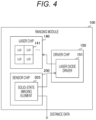
- Fig. 4 is a block diagram illustrating an example configuration of the ranging module 100 according to the first embodiment of the present technology.
- the ranging module 100 includes the laser chip 140, the driver chip 150, and the sensor chip 200.
- a plurality of laser diodes 141 is arranged in the laser chip 140.
- vertical cavity surface emitting lasers VCSELs
- a laser diode driver 151 is disposed in the driver chip 150.
- a solid-state imaging element 205 is disposed in the sensor chip 200.
- the laser diodes 141 emit light in response to driving by the laser diode driver 151.
- the laser diode driver 151 drives the laser diodes 141 in accordance with a light emission command supplied from the solid-state imaging element 205.
- the solid-state imaging element 205 measures the distance to an object for each measurement pixel 230 by a direct ToF (dToF) method, and outputs distance data.
- dToF direct ToF
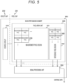
- Fig. 5 is a block diagram illustrating an example configuration of the solid-state imaging element 205 according to the first embodiment of the present technology.
- the solid-state imaging element 205 includes a control circuit 210, a pixel array unit 220, and a signal processing unit 250.
- the measurement pixel region 221 and the reference pixel region 222 are disposed.
- the plurality of measurement pixels 230 is arranged in the measurement pixel region 221, and the predetermined number of reference pixels 240 are arranged in the reference pixel region 222.
- These pixels are arranged in the pixel chip 201. Note that some of the elements in the respective pixels may be disposed in the pixel chip 201, and the remaining elements may be disposed in the circuit chip 202.
- Each measurement pixel 230 includes a photodiode such as a single-photon avalanche diode (SPAD), a resistor, and a transistor, and generates a pulse signal when reflected light enters.
- the circuit configuration of each reference pixel 240 is similar to that of each measurement pixel 230. However, as described above, the reference pixels 240 are disposed on the irradiation side of the two sides of the light blocking wall 121. Therefore, the length of the optical path in which irradiation light from the laser diodes 141 is reflected in the ranging module 100 and enters the reference pixels 240 is extremely short.
- the control circuit 210 controls the potential of each pixel.
- the signal processing unit 250 measures a distance for each measurement pixel 230, on the basis of signals from the respective measurement pixels 230 and the respective reference pixels 240.
- Fig. 6 is a block diagram illustrating an example configuration of the signal processing unit 250 according to the first embodiment of the present technology.
- the signal processing unit 250 includes time-to-digital converters (TDCs) 251 for the respective columns, and a measurement processing unit 252.
- TDCs time-to-digital converters
- a pulse signal OUT that is output from the pixels (measurement pixels 230 or reference pixels 240) in a column is supplied to the TDC 251 of the column.
- TDCs time-to-digital converters
- M being an integer of 1 or greater
- Each TDC 251 measures the time from the output timing of a light emission command to the laser diode driver 151 till the rising timing of the pulse signal OUT (in other words, the light reception timing).
- the measurement processing unit 252 measures a distance for each measurement pixel 230.
- the measurement processing unit 252 outputs the light emission command to the laser diode driver 151, and controls the TDC 251 of each column to start clocking.
- the TDC 251 of each column then stops clocking when the pulse signal of the corresponding column rises, and passes time information indicating the clocked time t on to the measurement processing unit 252.
- the measurement processing unit 252 generates a histogram on the basis of these times t.
- dToF distance measurement is performed on the basis of a difference between a timing t0 of light emission by the light source (laser diodes 141) and a timing t1 of light reception by the measurement pixel 230, using the following expression.
- D c / 2 ⁇ t 1 ⁇ t 0
- D represents the distance
- the unit is meter (m), for example.
- c represents the speed of light
- the unit is meter per second (m/s), for example.
- the laser diode driver 151 drives the laser diodes 141 in accordance with a light emission command from the measurement processing unit 252, and causes the laser diodes 141 to emit light. At this point of time, there is some time lag between the light emission command and the actual light emission from the laser diodes 141. This time lag is caused by a time constant in the path from the measurement processing unit 252 to the laser diodes 141, variations in characteristics due to temperature or aging of the laser diodes 141, or the like, and is difficult to predict.
- the reference pixels 240 are disposed at positions where the optical path length from the laser diodes 141 to the reference pixels 240 is extremely short. With this arrangement, the difference between the timing of light reception and the timing of light emission by the reference pixels 240 can be regarded as zero. Thus, the timing of light reception by the reference pixels 240 can be regarded as the light emission timing.
- the measurement processing unit 252 creates a histogram by performing acquisition of time information a plurality of times (thousands to tens of thousands of times, for example) for each pixel, and acquires a peak value of the created histogram as the timing of light reception by the pixel.
- the measurement processing unit 252 assigns the timing of light reception by the reference pixel 240 to t0 in Expression 1, and the timing of light reception by the measurement pixel 230 to t1 in Expression 1, and thus, obtains a distance D for each measurement pixel 230. Note that details of a ranging method using the reference pixels 240 are disclosed in Japanese Patent Application Laid-Open No. 2020-139810 .
- Fig. 7 is an example of a perspective view and cross-sectional views of a ranging module according to the comparative example.
- the laser chip 140 and the driver chip 150 are not shown.
- "a” illustrates a perspective view of the comparative example
- "b” illustrates a cross-sectional view of the comparative example as viewed from the X-axis direction.
- "c” illustrates a cross-sectional view of the comparative example as viewed from the Y-axis direction.
- the sensor chip 200 is electrically connected to the support substrate 130 by wires 139 in the comparative example. Therefore, as illustrated as an example in “b” and “c” of the drawing, a gap of a certain size is formed between the lower end of the light blocking wall 121 and the light receiving surface of the sensor chip 200 so that the lower end of the light blocking wall 121 does not come into contact with the wires 139.
- irradiation light might leak to the light receiving side through the gap. This makes it difficult to distinguish between reflected light outside the ranging module 100 and scattered light inside the ranging module 100. As a result, the short-distance measuring range is particularly limited.
- peak separation between the internal scattered light and the reflected light requires calculation costs.
- the measurement pixels 230 and the reference pixels 240 should be separated from each other. In that case, however, a situation in which different rays of reflected light are received by one pixel due to parallax easily occurs, and it becomes difficult to detect light that is reflected over a long distance and is simultaneously obtained with light reflected over a short distance. In this case, missed detection of an object at a long distance, or, in other words, occlusion occurs.
- openings are formed in the support substrate 130, the sensor chip 200 is flip-chip mounted on the back surface thereof, and the light blocking wall 121 is provided.
- the gap at the lower end of the light blocking wall 121 can be omitted, and light leakage can be reduced.
- the solid-state imaging element 205 measures distance, on the assumption that the light reception timing of the reference pixels 240 is the light emission timing.
- pixels different from the reference pixels 240 may be disposed on the irradiation side.
- a ranging module 100 according to a modification of the first embodiment differs from that of the first embodiment in that monitor pixels are provided in place of the reference pixels 240.
- monitor pixels 401 are arranged in place of the reference pixels 240, and a control unit 500 is further provided.
- Fig. 8 is a block diagram illustrating an example configuration of the monitor pixels 401, the measurement pixels 230, and the control unit 500 according to the modification of the first embodiment of the present technology.
- the control unit 500 an inter-pixel average acquisition unit 510, a time average acquisition unit 520, and a potential control unit 530 are provided.
- Each monitor pixel 401 includes a photoelectric conversion element 211, a p-channel metal oxide semiconductor (pMOS) transistor 311, a timing detection circuit 320, a sample-and-hold circuit 330, and buffers 340 and 350.
- pMOS metal oxide semiconductor
- the pMOS transistor 311 is inserted between a power supply potential VE and the photoelectric conversion element 211. Further, a control signal RCH from a timing generation unit 220 is input to the gate of the pMOS transistor 311. When the control signal RCH at the low level is input, the pMOS transistor 311 supplies the power supply potential VE to a connection node 312 between the pMOS transistor 311 and the photoelectric conversion element 211.
- the photoelectric conversion element 211 outputs a photocurrent by photoelectric conversion, depending on photon incidence.
- a SPAD is used as the photoelectric conversion element 211.
- the cathode of the photoelectric conversion element 211 is connected to the connection node 312, and its cathode potential Vs corresponds to the potential of the monitoring target.
- the anode of the photoelectric conversion element 211 is connected to the control unit 500, and its anode potential VSPAD is controlled by the control unit 500.
- a buffer 340 is inserted between the connection node 312 and the sample-and-hold circuit 330.
- the timing detection circuit 320 monitors the cathode potential Vs, and detects the timing at which a predetermined period of time has elapsed since the potential Vs started dropping with respect to the potential (which is the power supply potential VE) supplied by the pMOS transistor 311. In a case where the cathode potential Vs is the monitoring target, the cathode potential Vs becomes lower than the power supply potential VE when a photocurrent flows depending on photon incidence. Note that the monitor pixel 401 can also monitor the anode potential, as described later. When the anode potential is monitored, the timing at which a predetermined period of time has elapsed since the anode potential started increasing is detected.
- the sample-and-hold circuit 330 takes in and holds the cathode potential Vs on the basis of the timing detected by the timing detection circuit 320.
- the sample-and-hold circuit 330 outputs the held potential as a holding potential Vs_SH to a buffer 350.
- the buffer 350 is inserted between the sample-and-hold circuit 330 and the control unit 500.
- the buffer 250 is not necessarily provided, and it is possible to design a configuration in which the buffer 250 is not provided.
- two or more buffers 340, and two or more buffers 350 may be provided.
- a photoelectric conversion element 212 a pMOS transistor 381, and an inverter 382 are provided in each measurement pixel 230.
- connection configuration between the pMOS transistor 381 and the photoelectric conversion element 212 is similar to that between the pMOS transistor 311 and the photoelectric conversion element 211 in each monitor pixel 401.
- the inverter 382 inverts a signal of the cathode potential of the photoelectric conversion element 212, and supplies the inverted signal as a pulse signal of the measurement pixel 230 to a multiplexer 231 (or a multiplexer 232).
- each monitor pixel 401 of the plurality of monitor pixels 401 supplies the holding potential Vs_SH to the inter-pixel average acquisition unit 510.
- a holding potential of the m-th (m being an integer) monitor pixel 401 is defined as Vs_SHm. Note that the monitor pixels 401 are an example of the second pixel of the claims.
- the inter-pixel average acquisition unit 510 obtains an average of the respective holding potentials Vs_SHm of the plurality of monitor pixels 401 as an inter-pixel average Vs_SHAVp.
- the inter-pixel average acquisition unit 510 supplies the inter-pixel average Vs_SHAVp to the time average acquisition unit 520.
- the time average acquisition unit 520 obtains a time average Vs_SHAVt of the inter-pixel average Vs_SHAVp.
- the time average acquisition unit 520 supplies the time average Vs_SHAVt to the potential control unit 530.
- the potential control unit 530 controls the anode potential VSPAD to a lower potential when the time average Vs_SHAVt of held cathode potentials is higher. All the anodes of the plurality of monitor pixels 401 and the plurality of measurement pixels 230 are commonly connected to the potential control unit 530, and the potential control unit 530 controls the potentials of these anodes. Note that, when the monitor pixels 401 monitor the anode potentials, the cathode potentials are controlled by the potential control unit 530.
- each monitor pixel 401 one (the cathode, for example) of the anode and the cathode of the photoelectric conversion element 211 is connected to the connection node 312.
- the pMOS transistor 311 supplies the power supply potential VE to the connection node 312, in accordance with the control signal RCH.
- the timing detection circuit 320 detects the timing at which a predetermined period of time has elapsed since the cathode potential Vs of the connection node 312 started dropping with respect to the power supply potential VE. This timing corresponds to the timing at which a predetermined delay time has elapsed since the cathode potential dropped to a lower value than the threshold of the inverter 321.
- the sample-and-hold circuit 330 takes in and holds the cathode potential Vs as the holding potential Vs_SH, on the basis of the timing detected by the timing detection circuit 320.
- the control unit 500 then controls the other one (the anode, for example) of the anode and the cathode of the photoelectric conversion element 211 to a lower potential when the holding potential Vs_SH is higher.
- the buffer 340 is inserted into the stage preceding the sample-and-hold circuit 330, so that the capacitances of the connection nodes of the respective monitor pixels 401 and the respective measurement pixels 230 can be equalized.
- This connection node is the connection node between the photoelectric conversion element and the pMOS transistor.
- the breakdown voltages VBD of the respective monitor pixels 401 and the respective measurement pixels 230 can be equalized.
- Fig. 9 is a circuit diagram illustrating an example configuration of the control unit 500 according to the first embodiment of the present technology.
- the inter-pixel average acquisition unit 510 a plurality of resistors 511 and a capacitor 512 are provided.
- the resistors 511 are provided for the respective monitor pixels 401.
- a variable resistor 521 and a variable capacitor 522 are provided in the time average acquisition unit 520.
- an amplifier 531 is provided in the potential control unit 530.
- each resistor 511 is connected to each corresponding monitor pixel 401, and the other end thereof is connected to one end of the capacitor 512 and the time average acquisition unit 520. That is, the plurality of resistors 511 is connected in parallel between the plurality of monitor pixels 401 and the capacitor 512. The other end of the capacitor 512 is connected to the ground potential.
- the average potential of the holding potentials Vs_SH m of the plurality of monitor pixels 401 is generated as the inter-pixel average Vs_SH AVp , and is held in the capacitor 512.
- Obtaining the inter-pixel average can inhibit an adverse effect due to variation in the holding potential Vs_SH among the pixels.
- variable resistor 521 is connected to the inter-pixel average acquisition unit 510, and the other end is connected to one end of the variable capacitor 522 and the potential control unit 530.
- the other end of the variable capacitor 522 is connected to the ground potential.
- the circuit formed with the variable resistor 521 and the variable capacitor 522 functions as an analog low-pass filter that generates the time average Vs_SH AVt of the inter-pixel average Vs_SH AVp .
- the time average Vs_SH AVt is input to an inverting input terminal (-) of the amplifier 531, and a predetermined power supply potential is input to a non-inverting input terminal (+) of the amplifier 531.
- the amplifier 531 generates a result of comparison between those potentials as VSPAD according to the following expression, and supplies VSPAD to the anodes of the monitor pixels 401 and the measurement pixels 230.
- VSPAD Av VREF ⁇ Vs _ SH AVt
- Fig. 10 is a diagram illustrating an example of fluctuations of the cathode potential Vs and the anode potential VSPAD according to the first embodiment of the present technology.
- the power supply potential VE is supplied by the pMOS transistor 311, and the cathode potential Vs is the power supply potential VE.
- the cathode potential Vs drops to a bottom potential VBT, and returns to the original power supply potential VE by recharging.
- the voltage between the power supply potential VE and the bottom potential VBT is called an excess bias VEX.
- the voltage between the bottom potential VBT and the anode potential VSPAD is called the breakdown voltage VBD.
- the excess bias VEX fluctuates depending on variation in the breakdown voltage VBD and the temperature.
- the control unit 500 makes the anode potential VSPAD lower, when the holding potential at a time of decrease of the cathode potential Vs is higher. As a result, the breakdown voltage VBD becomes higher, and the excess bias VEX increases, to enhance PDE. Note that details of a potential control method using the monitor pixels 401 are disclosed in Japanese Patent Application Laid-Open No. 2021-56016 .
- the monitor pixels 401 are provided in place of the reference pixels 240, but both the reference pixels 240 and the monitor pixels 401 may be disposed on the irradiation side.
- the control circuit 210 makes the anode potential VSPAD lower when the holding potential at a time of decrease of the cathode potential Vs is higher.
- PDE can be increased.
- the laser chip 140 and the driver chip 150 are connected to the front surface of the support substrate 130. With this configuration, however, it is difficult to further reduce the thickness and the area of the ranging module 100.
- the thickness indicates the size in the Z-axis direction.
- a ranging module 100 according to a second embodiment differs from that of the first embodiment in that the laser chip 140 and the driver chip 150 are connected to the back surface of the support substrate 130.
- Fig. 11 is an example of a cross-sectional view of the ranging module 100 according to the second embodiment of the present technology.
- the ranging module 100 according to the second embodiment differs from that of the first embodiment in that the laser chip 140 and the driver chip 150 are flip-chip mounted on the back surface of the support substrate 130.
- a third opening for guiding irradiation light is further formed in the range from a coordinate X9 to a coordinate X10 below the lens 112.
- the laser chip 140 is connected immediately below the opening, with the light emitting surface facing upward. Note that the opening from the coordinate X9 to the coordinate X10 is an example of the third opening of the claims.
- the opening is added, and the laser chip 140 and the driver chip 150 are connected to the back surface of the support substrate 130, so that the chips and the wires on the front surface side of the support substrate 130 can be reduced.
- the thickness of the sealing member 120 can be reduced by the amount equivalent to the eliminated chips and wires, and the thickness of the ranging module 100 can be reduced by corresponding amount. Further, it is no longer necessary to seal the chips in the sealing member 120, and thus, the area of the sealing member 120 can be made smaller than that in the first embodiment.
- the laser chip 140 and the driver chip 150 are connected by bumps, so that the wiring length can be made shorter, and parasitic inductance can be made lower than those in the first embodiment in which wire bonding is performed.
- the output of the laser diodes 141 can be made greater to enable distance measurement over a longer distance.
- Fig. 12 is an example of a perspective view of the ranging module 100 according to the second embodiment of the present technology. As illustrated as an example in the drawing, an opening is added to the irradiation side, and the opening guides irradiation light from the laser diodes 141.
- an opening is added to the support substrate 130, and the laser chip 140 and the driver chip 150 are connected to the back surface of the support substrate 130.
- the thickness of the ranging module 100 can be reduced, and the area of the ranging module 100 can be made smaller.
- a ranging module 100 differs from that of the first embodiment in that the laser chip 140 is connected to the back surface of the support substrate 130.
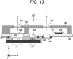
- Fig. 13 is an example of a cross-sectional view of the ranging module 100 according to the third embodiment of the present technology.
- the ranging module 100 according to the third embodiment differs from that of the first embodiment in that the laser chip 140 is flip-chip mounted on the back surface of the support substrate 130.
- a third opening for guiding irradiation light is further formed in the support substrate 130.
- the laser chip 140 is connected immediately below the opening, with the light emitting surface facing upward.
- the opening is added, and the laser chip 140 is connected to the back surface of the support substrate 130, so that the laser chip 140 and wires 149 on the front surface side of the support substrate 130 can be reduced. Since the space on the front surface necessary for the wires 149 for connecting the laser chip 140 is unnecessary, the area of the ranging module 100 can be reduced by corresponding amount.
- an opening is added to the support substrate 130, and the laser chip 140 is connected to the back surface of the support substrate 130.
- the area of the ranging module 100 can be made smaller.
- a ranging module 100 according to a fourth embodiment differs from that of the first embodiment in that the laser chip 140 and the driver chip 150 are stacked.
- Fig. 14 is an example of a cross-sectional view of the ranging module 100 according to the fourth embodiment of the present technology.
- the ranging module 100 of the fourth embodiment differs from that of the first embodiment in that the laser chip 140 is stacked on the upper surface of the driver chip 150, with the light emitting surface facing upward.
- the stacked chip is electrically connected to the front surface of the support substrate 130 by wires 149.
- the laser chip 140 is stacked on the driver chip 150, so that the area on the support substrate 130 necessary for mounting the chips can be made smaller than that in the first embodiment.
- the area of the ranging module 100 can be made smaller than that in the first embodiment.
- the areas of the driver chip 150 and the laser chip 140 are made substantially the same as each other, but the present embodiment is not limited to this configuration. As illustrated as an example in Fig. 15 , the area of the laser chip 140 on the upper side can be made smaller than that of the driver chip 150.
- the laser chip 140 is stacked on the driver chip 150, and thus, the area of the ranging module 100 can be made smaller.
- a ranging module 100 according to a fifth embodiment differs from that of the first embodiment in that the stacked chip is connected by solder balls.
- a BGA is used as the stacked chip, so that the wires on the front surface side of the support substrate 130 can be reduced.
- the thickness of the sealing member 120 can be reduced by the amount equivalent to the eliminated wires, and the thickness of the ranging module 100 can be reduced by corresponding amount.
- a BGA is used as the stacked chip formed with the laser chip 140 and the driver chip 150, and thus, the thickness of the ranging module 100 can be reduced.
- a ranging module 100 differs from that of the first embodiment in that the laser chip 140 and the driver chip 150 are stacked, and are then connected to the back surface of the support substrate 130.
- Fig. 17 is an example of a cross-sectional view of the ranging module 100 according to the sixth embodiment of the present technology.
- the ranging module 100 of the sixth embodiment differs from that of the first embodiment in that the laser chip 140 is stacked on the upper surface of the driver chip 150, with the light emitting surface facing upward.
- the stacked chip is flip-chip mounted on the back surface of the support substrate 130.
- a third opening for guiding irradiation light is further formed in the range from the coordinate X9 to the coordinate X10.
- the stacked chip is connected immediately below the opening, with the light emitting surface facing upward.
- the opening is added, and the stacked chip formed with the laser chip 140 and the driver chip 150 is connected to the back surface of the support substrate 130, so that the chips and the wires on the front surface side of the support substrate 130 can be reduced.
- the thickness of the sealing member 120 can be reduced by the amount equivalent to the eliminated chips and wires, and the thickness of the ranging module 100 can be reduced by corresponding amount. Further, it is no longer necessary to seal the chips in the sealing member 120, and thus, the area of the sealing member 120 can be made smaller than that in the first embodiment.
- an opening is added to the support substrate 130, and a stacked chip is connected to the back surface of the support substrate 130.
- the thickness of the ranging module 100 can be reduced, and the area of the ranging module 100 can be made smaller.
- the technology according to the present disclosure can be applied to various products.
- the technology according to the present disclosure may be realized as a device mounted on any type of mobile body such as an automobile, an electric vehicle, a hybrid electric vehicle, a motorcycle, a bicycle, a personal mobility, an airplane, a drone, a ship, or a robot.
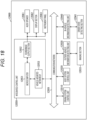
- Fig. 18 is a block diagram depicting an example of schematic configuration of a vehicle control system as an example of a mobile body control system to which the technology according to an embodiment of the present disclosure can be applied.
- the vehicle control system 12000 includes a plurality of electronic control units connected to each other via a communication network 12001.
- the vehicle control system 12000 includes a driving system control unit 12010, a body system control unit 12020, an outside-vehicle information detecting unit 12030, an in-vehicle information detecting unit 12040, and an integrated control unit 12050.
- a microcomputer 12051, a sound/image output section 12052, and a vehicle-mounted network interface (I/F) 12053 are illustrated as functional components of the integrated control unit 12050.
- the driving system control unit 12010 controls the operation of devices related to the driving system of the vehicle in accordance with various kinds of programs.
- the driving system control unit 12010 functions as a control device for a driving force generating device for generating the driving force of the vehicle, such as an internal combustion engine, a driving motor, or the like, a driving force transmitting mechanism for transmitting the driving force to wheels, a steering mechanism for adjusting the steering angle of the vehicle, a braking device for generating the braking force of the vehicle, and the like.
- the body system control unit 12020 controls the operation of various kinds of devices provided to a vehicle body in accordance with various kinds of programs.
- the body system control unit 12020 functions as a control device for a keyless entry system, a smart key system, a power window device, or various kinds of lamps such as a headlamp, a backup lamp, a brake lamp, a turn signal, a fog lamp, or the like.
- radio waves transmitted from a mobile device as an alternative to a key or signals of various kinds of switches can be input to the body system control unit 12020.
- the body system control unit 12020 receives these input radio waves or signals, and controls a door lock device, the power window device, the lamps, or the like of the vehicle.
- the outside-vehicle information detecting unit 12030 detects information about the outside of the vehicle including the vehicle control system 12000.
- the outside-vehicle information detecting unit 12030 is connected with an imaging section 12031.
- the outside-vehicle information detecting unit 12030 makes the imaging section 12031 image an image of the outside of the vehicle, and receives the imaged image.
- the outside-vehicle information detecting unit 12030 may perform processing of detecting an object such as a human, a vehicle, an obstacle, a sign, a character on a road surface, or the like, or processing of detecting a distance thereto.
- the imaging section 12031 is an optical sensor that receives light, and which outputs an electric signal corresponding to a received light amount of the light.
- the imaging section 12031 can output the electric signal as an image, or can output the electric signal as information about a measured distance.
- the light received by the imaging section 12031 may be visible light, or may be invisible light such as infrared rays or the like.
- the in-vehicle information detecting unit 12040 detects information about the inside of the vehicle.
- the in-vehicle information detecting unit 12040 is, for example, connected with a driver state detecting section 12041 that detects the state of a driver.
- the driver state detecting section 12041 for example, includes a camera that images the driver.
- the in-vehicle information detecting unit 12040 may calculate a degree of fatigue of the driver or a degree of concentration of the driver, or may determine whether the driver is dozing.
- the microcomputer 12051 can calculate a control target value for the driving force generating device, the steering mechanism, or the braking device on the basis of the information about the inside or outside of the vehicle which information is obtained by the outside-vehicle information detecting unit 12030 or the in-vehicle information detecting unit 12040, and output a control command to the driving system control unit 12010.
- the microcomputer 12051 can perform cooperative control intended to implement functions of an advanced driver assistance system (ADAS) which functions include collision avoidance or shock mitigation for the vehicle, following driving based on a following distance, vehicle speed maintaining driving, a warning of collision of the vehicle, a warning of deviation of the vehicle from a lane, or the like.
- ADAS advanced driver assistance system
- the microcomputer 12051 can perform cooperative control intended for automated driving, which makes the vehicle to travel automatedly without depending on the operation of the driver, or the like, by controlling the driving force generating device, the steering mechanism, the braking device, or the like on the basis of the information about the outside or inside of the vehicle which information is obtained by the outside-vehicle information detecting unit 12030 or the in-vehicle information detecting unit 12040.
- the microcomputer 12051 can output a control command to the body system control unit 12020 on the basis of the information about the outside of the vehicle which information is obtained by the outside-vehicle information detecting unit 12030.
- the microcomputer 12051 can perform cooperative control intended to prevent a glare by controlling the headlamp so as to change from a high beam to a low beam, for example, in accordance with the position of a preceding vehicle or an oncoming vehicle detected by the outside-vehicle information detecting unit 12030.
- the sound/image output section 12052 transmits an output signal of at least one of a sound and an image to an output device capable of visually or auditorily notifying information to an occupant of the vehicle or the outside of the vehicle.
- an audio speaker 12061, a display section 12062, and an instrument panel 12063 are illustrated as the output device.
- the display section 12062 may, for example, include at least one of an on-board display and a head-up display.
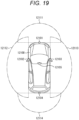
- Fig. 19 is a diagram depicting an example of the installation position of the imaging section 12031.
- the imaging section 12031 includes imaging sections 12101, 12102, 12103, 12104, and 12105.
- the imaging sections 12101, 12102, 12103, 12104, and 12105 are, for example, disposed at positions on a front nose, sideview mirrors, a rear bumper, and a back door of the vehicle 12100 as well as a position on an upper portion of a windshield within the interior of the vehicle.
- the imaging section 12101 provided to the front nose and the imaging section 12105 provided to the upper portion of the windshield within the interior of the vehicle obtain mainly an image of the front of the vehicle 12100.
- the imaging sections 12102 and 12103 provided to the sideview mirrors obtain mainly an image of the sides of the vehicle 12100.
- the imaging section 12104 provided to the rear bumper or the back door obtains mainly an image of the rear of the vehicle 12100.
- the imaging section 12105 provided to the upper portion of the windshield within the interior of the vehicle is used mainly to detect a preceding vehicle, a pedestrian, an obstacle, a signal, a traffic sign, a lane, or the like.
- FIG. 19 depicts an example of imaging ranges of the imaging sections 12101 to 12104.
- An imaging range 12111 represents the imaging range of the imaging section 12101 provided to the front nose.
- Imaging ranges 12112 and 12113 respectively represent the imaging ranges of the imaging sections 12102 and 12103 provided to the sideview mirrors.
- An imaging range 12114 represents the imaging range of the imaging section 12104 provided to the rear bumper or the back door.
- a bird's-eye image of the vehicle 12100 as viewed from above is obtained by superimposing image data imaged by the imaging sections 12101 to 12104, for example.
- At least one of the imaging sections 12101 to 12104 may have a function of obtaining distance information.
- at least one of the imaging sections 12101 to 12104 may be a stereo camera constituted of a plurality of imaging elements, or may be an imaging element having pixels for phase difference detection.
- the microcomputer 12051 can determine a distance to each three-dimensional object within the imaging ranges 12111 to 12114 and a temporal change in the distance (relative speed with respect to the vehicle 12100) on the basis of the distance information obtained from the imaging sections 12101 to 12104, and thereby extract, as a preceding vehicle, a nearest three-dimensional object in particular that is present on a traveling path of the vehicle 12100 and which travels in substantially the same direction as the vehicle 12100 at a predetermined speed (for example, equal to or more than 0 km/hour). Further, the microcomputer 12051 can set a following distance to be maintained in front of a preceding vehicle in advance, and perform automatic brake control (including following stop control), automatic acceleration control (including following start control), or the like. It is thus possible to perform cooperative control intended for automated driving that makes the vehicle travel automatedly without depending on the operation of the driver or the like.
- automatic brake control including following stop control
- automatic acceleration control including following start control
- the microcomputer 12051 can classify three-dimensional object data on three-dimensional objects into three-dimensional object data of a two-wheeled vehicle, a standard-sized vehicle, a large-sized vehicle, a pedestrian, a utility pole, and other three-dimensional objects on the basis of the distance information obtained from the imaging sections 12101 to 12104, extract the classified three-dimensional object data, and use the extracted three-dimensional object data for automatic avoidance of an obstacle.
- the microcomputer 12051 identifies obstacles around the vehicle 12100 as obstacles that the driver of the vehicle 12100 can recognize visually and obstacles that are difficult for the driver of the vehicle 12100 to recognize visually. Then, the microcomputer 12051 determines a collision risk indicating a risk of collision with each obstacle.
- the microcomputer 12051 In a situation in which the collision risk is equal to or higher than a set value and there is thus a possibility of collision, the microcomputer 12051 outputs a warning to the driver via the audio speaker 12061 or the display section 12062, and performs forced deceleration or avoidance steering via the driving system control unit 12010. The microcomputer 12051 can thereby assist in driving to avoid collision.
- At least one of the imaging sections 12101 to 12104 may be an infrared camera that detects infrared rays.
- the microcomputer 12051 can, for example, recognize a pedestrian by determining whether or not there is a pedestrian in imaged images of the imaging sections 12101 to 12104. Such recognition of a pedestrian is, for example, performed by a procedure of extracting characteristic points in the imaged images of the imaging sections 12101 to 12104 as infrared cameras and a procedure of determining whether or not it is the pedestrian by performing pattern matching processing on a series of characteristic points representing the contour of the object.
- the sound/image output section 12052 controls the display section 12062 so that a square contour line for emphasis is displayed so as to be superimposed on the recognized pedestrian.
- the sound/image output section 12052 may also control the display section 12062 so that an icon or the like representing the pedestrian is displayed at a desired position.
- the technology according to the present disclosure can be applied to, for example, the outside-vehicle information detecting unit 12030 among the components described above.
- the ranging module 100 in Fig. 1 can be applied to the outside-vehicle information detecting unit 12030.
Landscapes
- Engineering & Computer Science (AREA)
- Physics & Mathematics (AREA)
- Computer Networks & Wireless Communication (AREA)
- General Physics & Mathematics (AREA)
- Radar, Positioning & Navigation (AREA)
- Remote Sensing (AREA)
- Electromagnetism (AREA)
- Optical Radar Systems And Details Thereof (AREA)
- Solid State Image Pick-Up Elements (AREA)
- Measurement Of Optical Distance (AREA)
Abstract
Description
- The present technology relates to a ranging module. More particularly, the present technology relates to a ranging module that emits irradiation light and receives reflected light.
- For ranging modules, a ranging method called the time of flight (ToF) method has been known. The ToF method is a method for measuring a distance by irradiating an object with irradiation light from an electronic device, and obtaining the round-trip time required until the irradiation light is reflected and returned to the electronic device. For example, a module has been proposed, and, in the module, a light emitting element that emits irradiation light and a light receiving element that receives reflected light are provided on a substrate, and a light blocking wall is disposed between these elements (see
Patent Document 1, for example). In this module, a gap is formed between the light blocking wall and the substrate so that the lower surface of the light blocking wall does not come into contact with the substrate. - Patent Document 1:
Japanese Patent Application Laid-Open No. 2016-27657 - By the conventional technique described above, the gap is formed so that the lower surface of the light blocking wall does not come into contact with the substrate. With this arrangement, thermal expansion of the light blocking wall does not affect the substrate, and sensing performance is enhanced. In the module described above, however, irradiation light might leak to the light receiving side through the gap under the light blocking wall.
- The present technology has been made in view of such circumstances, and aims to reduce leakage of irradiation light to the light receiving side in a ranging module that uses the ToF method.
- The present technology has been made to solve the above problems, and a first aspect thereof is a ranging module that includes: a sensor chip that has a first pixel region and a second pixel region formed on a light receiving surface, a plurality of first pixels being provided in the first pixel region, a second pixel being provided in the second pixel region, the first pixels receiving reflected light of irradiation light from a light source, the second pixel being disposed between the first pixel region and the light source; a light blocking wall that is disposed between the first pixel region and the second pixel region; and a support substrate to which the sensor chip is connected, the support substrate having an opening through which the reflected light is guided to the first pixel region and the second pixel region. This brings about an effect of reducing leakage of irradiation light to the light receiving side.
- Also, in the first aspect, the opening may include a first opening and a second opening separated by a bridge portion that is part of the support substrate, the first opening may guide the reflected light to the first pixel region, and the second opening may guide the reflected light to the second pixel region. This brings about an effect of reliably reducing light leakage.
- Further, in the first aspect, the light blocking wall may be disposed in the bridge portion, and the width of the light shielding wall may be smaller than the distance between the first pixel region and the second pixel region. This brings about an effect of preventing reflected light from being blocked.
- Furthermore, in the first aspect, the ranging module may further include: a laser chip in which a plurality of laser diodes is provided as the light source; and a driver chip on which a laser diode driver that drives each laser diode of the plurality of laser diodes is disposed. In this ranging module, the sensor chip may be connected to the back surface on the opposite side of the support substrate from the front surface that is the surface on the light receiving side of the support substrate. This brings about an effect of causing the laser drivers to emit light when the laser drivers are driven by the laser diode driver.
- Further, in the first aspect, the laser chip may be disposed between the second pixel and the driver chip. This brings about an effect of causing light reflected in the ranging module to enter the second pixel.
- Furthermore, in the first aspect, the laser chip and the driver chip may be connected to the front surface of the support substrate. This brings about an effect of increasing the degree of freedom in selecting a laser diode and a laser diode driver.
- Further, in the first aspect, the laser chip and the driver chip may be connected to the back surface of the support substrate, and the opening may further include a third opening that guides the irradiation light from the laser chip. This brings about an effect of reducing the area and the thickness of the ranging module.
- Furthermore, in the first aspect, the laser chip may be connected to the back surface of the support substrate, the driver chip may be connected to the front surface of the support substrate, and the opening may further include a third opening that guides the irradiation light from the laser chip. This brings about an effect of reducing the area of the ranging module.
- Further, in the first aspect, the laser chip may be stacked on the driver chip. This brings about an effect of reducing the area of the ranging module.
- Furthermore, in the first aspect, the laser chip may be connected to the front surface of the support substrate by a wire. This brings about an effect of mounting the laser chip on the support substrate.
- Further, in the first aspect, the driver chip may be connected to the back surface of the support substrate by a solder ball. This brings about an effect of reducing the thickness of the ranging module.
- Furthermore, in the first aspect, the laser chip may be connected to the back surface of the support substrate, and the opening may further include a third opening that guides the irradiation light from the laser chip. This brings about an effect of reducing the thickness of the ranging module.
- Also, in the first aspect, the ranging module may further include a ranging processing unit. In this ranging module, the second pixel may include a reference pixel, and the ranging processing unit may obtain a distance in accordance with the time from a timing of light reception by the reference pixel till a timing of light reception by the first pixels. This brings about an effect of acquiring the light emission timing even if there is a time lag from a light emission command till light emission.
- Furthermore, in the first aspect, the ranging module may further include a control circuit. In this ranging module, the first pixels may include a first photodiode, the second pixel may include a monitor pixel, the monitor pixel may include a second photodiode and a sample-and-hold circuit, and the control circuit may supply a lower potential to the anodes of the first photodiode and the second photodiode when the holding potential of the sample-and-hold circuit is higher at a time of decrease in the potential of the cathode of the second photodiode due to light reception by the monitor pixel. This brings about an effect of reducing fluctuations of an excess bias.
-
-
Fig. 1 is an example of cross-sectional views of a ranging module according to a first embodiment of the present technology. -
Fig. 2 is an example of perspective views of the ranging module according to the first embodiment of the present technology. -
Fig. 3 is an example of cross-sectional views of the ranging module according to the first embodiment of the present technology, as viewed from another direction. -
Fig. 4 is a block diagram illustrating an example configuration of the ranging module according to the first embodiment of the present technology. -
Fig. 5 is a block diagram illustrating an example configuration of a solid-state imaging element according to the first embodiment of the present technology. -
Fig. 6 is a block diagram illustrating an example configuration of a signal processing unit according to the first embodiment of the present technology. -
Fig. 7 is an example of a perspective view and cross-sectional views of a ranging module according to a comparative example. -
Fig. 8 is a block diagram illustrating an example configuration of monitor pixels, measurement pixels, and a control unit according to a modification of the first embodiment of the present technology. -
Fig. 9 is a circuit diagram illustrating an example configuration of a control unit according to the first embodiment of the present technology. -
Fig. 10 is a diagram illustrating an example of fluctuations of a cathode potential and an anode potential according to the first embodiment of the present technology. -
Fig. 11 is an example of a cross-sectional view of a ranging module according to a second embodiment of the present technology. -
Fig. 12 is an example of a perspective view of the ranging module according to the second embodiment of the present technology. -
Fig. 13 is an example of a cross-sectional view of a ranging module according to a third embodiment of the present technology. -
Fig. 14 is an example of a cross-sectional view of a ranging module according to a fourth embodiment of the present technology. -
Fig. 15 is an example of a perspective view of a stacked chip according to the fourth embodiment of the present technology. -
Fig. 16 is an example of a cross-sectional view of a ranging module according to a fifth embodiment of the present technology. -
Fig. 17 is an example of a cross-sectional view of a ranging module according to a sixth embodiment of the present technology. -
Fig. 18 is a block diagram depicting an example of schematic configuration of a vehicle control system. -
Fig. 19 is an explanatory diagram depicting an example of an installation position of an imaging section. - Modes for carrying out the present technology (hereinafter referred to as embodiments) will be described below. The description will be given in the following order.
- 1. First embodiment (an example in which a sensor chip is connected to the back surface of a support substrate)
- 2. Second embodiment (an example in which all chips are connected to the back surface of a support substrate)
- 3. Third embodiment (an example in which a sensor chip and a laser chip are connected to the back surface of a support substrate)
- 4. Fourth embodiment (an example in which a sensor chip is connected to the back surface of a support substrate, and a stacked chip is wire-bonded to the front surface thereof)
- 5. Fifth embodiment (an example in which a sensor chip is connected to the back surface of a support substrate, and a stacked chip is connected to the front surface thereof by solder balls)
- 6. Sixth embodiment (an example in which a sensor chip and a stacked chip are connected to the back surface of a support substrate)
- 7. Example Application to a Mobile Body
-
Fig. 1 is an example of cross-sectional views of a rangingmodule 100 according to a first embodiment of the present technology. In the drawing, "a" illustrates a cross-sectional view of the rangingmodule 100 having an appropriate size, and "b" illustrates a cross-sectional view of the rangingmodule 100 partially having an inappropriate size. - The ranging
module 100 measures a distance to an object, and includeslenses member 120, anoptical filter 122, asupport substrate 130, alaser chip 140, adriver chip 150, and asensor chip 200. - Further, the optical axes of the
lenses module 100 as viewed from the Y-axis direction. - The
sensor chip 200 is a chip in which pixels that photoelectrically convert incident light are arranged, and includes apixel chip 201 and acircuit chip 202 that are stacked. These chips are electrically connected via a connecting portion such as a via. Note that the connection can also be made by Cu-Cu bonding or a bump, other than a via. The connection can also be made by a scheme (such as magnetic coupling) other than these schemes. Furthermore, although the two chips are stacked, three or more layers can be stacked. Alternatively, although thesensor chip 200 has a stacked structure,
it is also possible to form a single semiconductor chip without stacking. - In the
pixel chip 201, a plurality of pixels is arranged. These pixels include a plurality ofmeasurement pixels 230 and a predetermined number ofreference pixels 240. Hereinafter, the direction from thecircuit chip 202 toward thepixel chip 201 will be referred to as the "upward" direction, and the opposite direction will be referred to as the "downward" direction. - The plurality of
measurement pixels 230 is arranged in a two-dimensional lattice pattern in ameasurement pixel region 221 on the upper surface of thepixel chip 201. Meanwhile, thereference pixels 240 are arranged in areference pixel region 222 on the upper surface of thepixel chip 201. In the drawing, themeasurement pixels 230 are two-dimensionally arranged in the X-axis direction and the Y-axis direction, and thereference pixels 240 are also two-dimensionally arranged in the X-axis direction and the Y-axis direction. Note that themeasurement pixels 230 are an example of the first pixels disclosed in the claims, and thereference pixels 240 are an example of the second pixel disclosed in the claims. Also, thereference pixels 240 may be one-dimensionally arranged in the Y-axis direction or the like. - Further, in the X-axis direction, a certain distance is maintained between the
measurement pixel region 221 and thereference pixel region 222. In the drawing, the distance from a coordinate X2 to a coordinate X7 corresponds to the distance between themeasurement pixel region 221 and thereference pixel region 222. - Furthermore, the peripheries of the pixels (the
measurement pixels 230 and the reference pixels 240) on the upper surface of thepixel chip 201 are electrically connected to (in other words, are flip-chip mounted on) the lower surface of thesupport substrate 130 bybumps 209. - Two openings penetrating in the Z-axis direction are formed in the
support substrate 130. The opening from a coordinate X1 to a coordinate X3 guides reflected light of irradiation light to themeasurement pixel region 221, and the opening from a coordinate X6 to a coordinate X8 guides reflected light to thereference pixel region 222. The part of thesupport substrate 130 from the coordinate X3 to the coordinate X6 that separates these openings from each other will be hereinafter referred to as the "bridge portion". Note that the former opening is an example of the first opening disclosed in the claims, and the latter opening an example of the second opening disclosed in the claims. - Further, the surface on the light receiving side of the
support substrate 130 is referred to as the upper surface or the "front surface", and the surface on the opposite side from the upper surface will be referred to as the lower surface or the "back surface". Thelaser chip 140 and thedriver chip 150 are electrically connected to the front surface of thesupport substrate 130 bywires - A plurality of laser diodes (not illustrated) is arranged as a light source on the
laser chip 140. Further, a laser diode driver (not illustrated) is disposed on thedriver chip 150. The laser driver diode drives each laser diode of the plurality of laser diodes to emit irradiation light. As the irradiation light, invisible light such as infrared light is used, for example. - Furthermore, in the X-axis direction, the
reference pixel region 222 is disposed between thelaser chip 140 and themeasurement pixel region 221. The position of thedriver chip 150 is not limited, but is disposed near thelaser chip 140. - In the drawing, the
laser chip 140 and thedriver chip 150 are not stacked. Therefore, the degree of freedom in selecting a laser diode or a laser diode driver is higher than that in a case where those chips are stacked, as described later. Further, thesensor chip 200 is connected to the back surface of thesupport substrate 130, and thelaser chip 140 is connected to the front surface thereof. Accordingly, wiring interference between the chips can be eliminated, compared with a case where both of those chips are connected to the back surface. This makes it easier to shorten the base length from the light source (laser chip 140) to the light receiving unit (measurement pixel region 221). - The sealing
member 120 covers and seals the peripheries of the two openings of thesupport substrate 130, and thelaser chip 140 and thedriver chip 150 with outer walls. In this sealingmember 120, openings for attaching thelenses lens 111 is attached to a portion above themeasurement pixel region 221, and thelens 112 is attached to a portion above thelaser chip 140. - The
lens 111 condenses reflected light of irradiation light, and guides the reflected light to themeasurement pixel region 221 below thelens 111. Thelens 112 optically adjusts the irradiation light from thelaser chip 140 below thelens 112, and a collimating lens or the like is used. - Further, part of the outer walls of the sealing
member 120 extends downward, and the lower end thereof is in contact with the bridge portion of thesupport substrate 130. This portion serves as alight blocking wall 121 that blocks irradiation light. Thislight blocking wall 121 extends in the Y-axis direction, and the space inside the sealingmember 120 is separated into two spaces on the light receiving side and the irradiation side by thelight blocking wall 121. In the drawing, the portion from a coordinate X4 to a coordinate X5 corresponds to thelight blocking wall 121. - The
optical filter 122 passes light (infrared light or the like) in the same wavelength region as the irradiation light, and is disposed between thelens 111 and themeasurement pixel region 221. - Furthermore, as illustrated as an example in "a" of the drawing, the respective widths of the bridge portion and the
light blocking wall 121 are assumed to be narrower than the distance between themeasurement pixel region 221 and the reference pixel region 222 (which is the distance from the coordinate X2 to the coordinate X7). In "a" of the drawing, the distance from the coordinate X3 to the coordinate X6 is the width of the bridge portion, and the distance from the coordinate X4 to the coordinate X5 is the width of thelight blocking wall 121. - On the other hand, "b" of the drawing illustrates an inappropriate example in which the respective widths of the bridge portion and the
light blocking wall 121 are made equal to or greater than the distance between themeasurement pixel region 221 and the reference pixel region 222 (which is the distance from the coordinate X2 to the coordinate X7). In this example, there is a possibility that part of reflected light is blocked by the bridge portion and thelight blocking wall 121. As illustrated as an example in "a" of the drawing, the widths of the bridge portion and thelight blocking wall 121 are reduced, to prevent blocking of part of reflected light. - In summary, the
measurement pixel region 221 and thereference pixel region 222 are formed on the light receiving surface of thesensor chip 200. In themeasurement pixel region 221, a plurality ofmeasurement pixels 230 that receive reflected light of irradiation light from the light source (laser chip 140) is arranged. Thereference pixel region 222 is disposed between themeasurement pixel region 221 and the light source, and a predetermined number ofreference pixels 240 are arranged therein. Thelight blocking wall 121 is disposed between themeasurement pixel region 221 and thereference pixel region 222. - Further, two openings separated by the bridge portion from the coordinate X3 to the coordinate X6 are formed in the
support substrate 130. One of those openings guides reflected light to themeasurement pixel region 221, and the other guides reflected light to thereference pixel region 222. The former reflected light is the light reflected by an object outside the rangingmodule 100, and the latter reflected light is the light reflected inside the rangingmodule 100. - Note that an optical member (such as a mirror) that reflects irradiation light and guides the reflected light to the
reference pixel region 222 may be further disposed inside the sealingmember 120. -
Fig. 2 is an example of perspective views of the rangingmodule 100 according to the first embodiment of the present technology. In the drawing, "a" illustrates a perspective view of the rangingmodule 100, with thelens 111, thelens 112, the sealingmember 120, and theoptical filter 122 having been removed. In the drawing, "b" illustrates a perspective view of a state in which thelight blocking wall 121 has been added to "a" of the drawing. - As illustrated as an example in "a" of the drawing, the opening formed in the region surrounded by coordinates (X1, Y1), (X1, Y2), (X3, Y1), and (X3, Y2) in the X-Y plane guides reflected light to the
measurement pixels 230. Further, the opening formed in the region surrounded by coordinates (X6, Y3), (X6, Y4), (X8, Y3), and (X8, Y4) guides reflected light to thereference pixels 240. These openings are separated by the bridge portion in the region surrounded by coordinates (X3, Y1), (X3, Y2), (X6, Y3), and (X6, Y4). Note that the distance from Y1 to Y2, and the distance from Y3 to Y4 may be the same, or may be different. - As illustrated as an example in "b" of the drawing, the
light blocking wall 121 is disposed in the bridge portion, and the lower end thereof is in contact with the bridge portion. Alternatively, a slight gap is left between the lower end of thelight blocking wall 121 and the bridge portion within such a range in which influence of leakage of irradiation light on the light receiving side is avoided. Since there is almost no gap between the bridge portion and thelight blocking wall 121, it is possible to prevent irradiation light from leaking to the light receiving side. - Note that, although the two openings are separated by the bridge portion, the bridge portion may not be provided, and only one opening may be provided. In this case, a gap is formed between the lower end of the
light blocking wall 121 and the upper surface of thesensor chip 200. However, the gap is located at a lower position than the light source, and thus, light leakage hardly occurs. Furthermore, since only one opening is required to be formed, processing becomes easier. -
Fig. 3 is an example of cross-sectional views of the rangingmodule 100 according to the first embodiment of the present technology, as viewed from the X-axis direction. InFig. 3 , "a" illustrates a cross-sectional view taken along the line A1-A2 immediately below thelight blocking wall 121 in "b" ofFig. 2 . InFig. 3 , "b" illustrates a cross-sectional view taken along the line B1-B2 extending through the opening in "b" ofFig. 2 . - As illustrated as an example in "a" of
Fig. 3 , the lower end of thelight blocking wall 121 is in contact with the bridge portion of thesupport substrate 130. Further, as illustrated as an example in "b" ofFig. 3 , the portion from the coordinate Y3 to the coordinate Y4 is open. -
Fig. 4 is a block diagram illustrating an example configuration of the rangingmodule 100 according to the first embodiment of the present technology. The rangingmodule 100 includes thelaser chip 140, thedriver chip 150, and thesensor chip 200. - A plurality of
laser diodes 141 is arranged in thelaser chip 140. For example, vertical cavity surface emitting lasers (VCSELs) are used as thelaser diodes 141. Alaser diode driver 151 is disposed in thedriver chip 150. A solid-state imaging element 205 is disposed in thesensor chip 200. - The
laser diodes 141 emit light in response to driving by thelaser diode driver 151. Thelaser diode driver 151 drives thelaser diodes 141 in accordance with a light emission command supplied from the solid-state imaging element 205. - Further, the solid-
state imaging element 205 measures the distance to an object for eachmeasurement pixel 230 by a direct ToF (dToF) method, and outputs distance data. -
Fig. 5 is a block diagram illustrating an example configuration of the solid-state imaging element 205 according to the first embodiment of the present technology. The solid-state imaging element 205 includes acontrol circuit 210, apixel array unit 220, and asignal processing unit 250. In thepixel array unit 220, themeasurement pixel region 221 and thereference pixel region 222 are disposed. The plurality ofmeasurement pixels 230 is arranged in themeasurement pixel region 221, and the predetermined number ofreference pixels 240 are arranged in thereference pixel region 222. These pixels are arranged in thepixel chip 201. Note that some of the elements in the respective pixels may be disposed in thepixel chip 201, and the remaining elements may be disposed in thecircuit chip 202. - Each
measurement pixel 230 includes a photodiode such as a single-photon avalanche diode (SPAD), a resistor, and a transistor, and generates a pulse signal when reflected light enters. The circuit configuration of eachreference pixel 240 is similar to that of eachmeasurement pixel 230. However, as described above, thereference pixels 240 are disposed on the irradiation side of the two sides of thelight blocking wall 121. Therefore, the length of the optical path in which irradiation light from thelaser diodes 141 is reflected in the rangingmodule 100 and enters thereference pixels 240 is extremely short. - The
control circuit 210 controls the potential of each pixel. Thesignal processing unit 250 measures a distance for eachmeasurement pixel 230, on the basis of signals from therespective measurement pixels 230 and therespective reference pixels 240. -
Fig. 6 is a block diagram illustrating an example configuration of thesignal processing unit 250 according to the first embodiment of the present technology. Thesignal processing unit 250 includes time-to-digital converters (TDCs) 251 for the respective columns, and ameasurement processing unit 252. A pulse signal OUT that is output from the pixels (measurement pixels 230 or reference pixels 240) in a column is supplied to theTDC 251 of the column. Note that one set of aTDC 251 and ameasurement processing unit 252 for M (M being an integer of 1 or greater) pixels may be disposed immediately below thepixel array unit 220. - Each
TDC 251 measures the time from the output timing of a light emission command to thelaser diode driver 151 till the rising timing of the pulse signal OUT (in other words, the light reception timing). - The
measurement processing unit 252 measures a distance for eachmeasurement pixel 230. Themeasurement processing unit 252 outputs the light emission command to thelaser diode driver 151, and controls theTDC 251 of each column to start clocking. TheTDC 251 of each column then stops clocking when the pulse signal of the corresponding column rises, and passes time information indicating the clocked time t on to themeasurement processing unit 252. Themeasurement processing unit 252 generates a histogram on the basis of these times t. - Here, by the dToF method, distance measurement is performed on the basis of a difference between a timing t0 of light emission by the light source (laser diodes 141) and a timing t1 of light reception by the
measurement pixel 230, using the following expression.
- In the above expression, D represents the distance, and the unit is meter (m), for example. Further, c represents the speed of light, and the unit is meter per second (m/s), for example.
- As described above, the
laser diode driver 151 drives thelaser diodes 141 in accordance with a light emission command from themeasurement processing unit 252, and causes thelaser diodes 141 to emit light. At this point of time, there is some time lag between the light emission command and the actual light emission from thelaser diodes 141. This time lag is caused by a time constant in the path from themeasurement processing unit 252 to thelaser diodes 141, variations in characteristics due to temperature or aging of thelaser diodes 141, or the like, and is difficult to predict. - Therefore, as described above, the
reference pixels 240 are disposed at positions where the optical path length from thelaser diodes 141 to thereference pixels 240 is extremely short. With this arrangement, the difference between the timing of light reception and the timing of light emission by thereference pixels 240 can be regarded as zero. Thus, the timing of light reception by thereference pixels 240 can be regarded as the light emission timing. - The
measurement processing unit 252 creates a histogram by performing acquisition of time information a plurality of times (thousands to tens of thousands of times, for example) for each pixel, and acquires a peak value of the created histogram as the timing of light reception by the pixel. Themeasurement processing unit 252 then assigns the timing of light reception by thereference pixel 240 to t0 inExpression 1, and the timing of light reception by themeasurement pixel 230 to t1 inExpression 1, and thus, obtains a distance D for eachmeasurement pixel 230. Note that details of a ranging method using thereference pixels 240 are disclosed inJapanese Patent Application Laid-Open No. 2020-139810 - Here, a configuration in which any opening is not formed in the
support substrate 130, and thesensor chip 200 is connected to thesupport substrate 130 is discussed as a comparative example. -
Fig. 7 is an example of a perspective view and cross-sectional views of a ranging module according to the comparative example. In the drawing, thelaser chip 140 and thedriver chip 150 are not shown. In the drawing, "a" illustrates a perspective view of the comparative example, and "b" illustrates a cross-sectional view of the comparative example as viewed from the X-axis direction. In the drawing, "c" illustrates a cross-sectional view of the comparative example as viewed from the Y-axis direction. - As illustrated as an example in "a" of the drawing, the
sensor chip 200 is electrically connected to thesupport substrate 130 bywires 139 in the comparative example. Therefore, as illustrated as an example in "b" and "c" of the drawing, a gap of a certain size is formed between the lower end of thelight blocking wall 121 and the light receiving surface of thesensor chip 200 so that the lower end of thelight blocking wall 121 does not come into contact with thewires 139. In the configuration of the comparative example, irradiation light might leak to the light receiving side through the gap. This makes it difficult to distinguish between reflected light outside the rangingmodule 100 and scattered light inside the rangingmodule 100. As a result, the short-distance measuring range is particularly limited. Further, peak separation between the internal scattered light and the reflected light requires calculation costs. To avoid this, themeasurement pixels 230 and thereference pixels 240 should be separated from each other. In that case, however, a situation in which different rays of reflected light are received by one pixel due to parallax easily occurs, and it becomes difficult to detect light that is reflected over a long distance and is simultaneously obtained with light reflected over a short distance. In this case, missed detection of an object at a long distance, or, in other words, occlusion occurs. - On the other hand, in the configuration in
Fig. 1 in which the openings are formed in thesupport substrate 130, and thesensor chip 200 is flip-chip mounted on the back surface thereof, there is no need to avoid the wires on the front surface side, and thus, the lower end of thelight blocking wall 121 can be brought into contact with the bridge portion of thesupport substrate 130. This can reduce leakage of irradiation light. As light leakage is reduced in this manner, the distance measurement range on the short distance side can be made wider than that in the comparative example. Also, the peak separation between the internal scattered light and the reflected light becomes unnecessary, and the calculation costs can be lowered. Further, the distance between themeasurement pixels 230 and thereference pixels 240 can be made closer to the width of thelight blocking wall 121, and thus, occlusion can be prevented. - As described above, according to the first embodiment of the present technology, openings are formed in the
support substrate 130, thesensor chip 200 is flip-chip mounted on the back surface thereof, and thelight blocking wall 121 is provided. Thus, the gap at the lower end of thelight blocking wall 121 can be omitted, and light leakage can be reduced. - In the first embodiment described above, the solid-
state imaging element 205 measures distance, on the assumption that the light reception timing of thereference pixels 240 is the light emission timing. However, pixels different from thereference pixels 240 may be disposed on the irradiation side. A rangingmodule 100 according to a modification of the first embodiment differs from that of the first embodiment in that monitor pixels are provided in place of thereference pixels 240. - In the modification of the first embodiment, monitor
pixels 401 are arranged in place of thereference pixels 240, and acontrol unit 500 is further provided. -
Fig. 8 is a block diagram illustrating an example configuration of themonitor pixels 401, themeasurement pixels 230, and thecontrol unit 500 according to the modification of the first embodiment of the present technology. In thecontrol unit 500, an inter-pixelaverage acquisition unit 510, a timeaverage acquisition unit 520, and apotential control unit 530 are provided. - Each
monitor pixel 401 includes aphotoelectric conversion element 211, a p-channel metal oxide semiconductor (pMOS)transistor 311, atiming detection circuit 320, a sample-and-hold circuit 330, and buffers 340 and 350. - The
pMOS transistor 311 is inserted between a power supply potential VE and thephotoelectric conversion element 211. Further, a control signal RCH from atiming generation unit 220 is input to the gate of thepMOS transistor 311. When the control signal RCH at the low level is input, thepMOS transistor 311 supplies the power supply potential VE to aconnection node 312 between thepMOS transistor 311 and thephotoelectric conversion element 211. - The
photoelectric conversion element 211 outputs a photocurrent by photoelectric conversion, depending on photon incidence. For example, a SPAD is used as thephotoelectric conversion element 211. The cathode of thephotoelectric conversion element 211 is connected to theconnection node 312, and its cathode potential Vs corresponds to the potential of the monitoring target. On the other hand, the anode of thephotoelectric conversion element 211 is connected to thecontrol unit 500, and its anode potential VSPAD is controlled by thecontrol unit 500. - A
buffer 340 is inserted between theconnection node 312 and the sample-and-hold circuit 330. - The
timing detection circuit 320 monitors the cathode potential Vs, and detects the timing at which a predetermined period of time has elapsed since the potential Vs started dropping with respect to the potential (which is the power supply potential VE) supplied by thepMOS transistor 311. In a case where the cathode potential Vs is the monitoring target, the cathode potential Vs becomes lower than the power supply potential VE when a photocurrent flows depending on photon incidence. Note that themonitor pixel 401 can also monitor the anode potential, as described later. When the anode potential is monitored, the timing at which a predetermined period of time has elapsed since the anode potential started increasing is detected. - The sample-and-
hold circuit 330 takes in and holds the cathode potential Vs on the basis of the timing detected by thetiming detection circuit 320. The sample-and-hold circuit 330 outputs the held potential as a holding potential Vs_SH to abuffer 350. - The
buffer 350 is inserted between the sample-and-hold circuit 330 and thecontrol unit 500. Note that thebuffer 250 is not necessarily provided, and it is possible to design a configuration in which thebuffer 250 is not provided. Alternatively, two ormore buffers 340, and two ormore buffers 350 may be provided. - Further, a
photoelectric conversion element 212, apMOS transistor 381, and aninverter 382 are provided in eachmeasurement pixel 230. - The connection configuration between the
pMOS transistor 381 and thephotoelectric conversion element 212 is similar to that between thepMOS transistor 311 and thephotoelectric conversion element 211 in eachmonitor pixel 401. - The
inverter 382 inverts a signal of the cathode potential of thephotoelectric conversion element 212, and supplies the inverted signal as a pulse signal of themeasurement pixel 230 to a multiplexer 231 (or a multiplexer 232). - Further, each
monitor pixel 401 of the plurality ofmonitor pixels 401 supplies the holding potential Vs_SH to the inter-pixelaverage acquisition unit 510. A holding potential of the m-th (m being an integer)monitor pixel 401 is defined as Vs_SHm. Note that themonitor pixels 401 are an example of the second pixel of the claims. - The inter-pixel
average acquisition unit 510 obtains an average of the respective holding potentials Vs_SHm of the plurality ofmonitor pixels 401 as an inter-pixel average Vs_SHAVp. The inter-pixelaverage acquisition unit 510 supplies the inter-pixel average Vs_SHAVp to the timeaverage acquisition unit 520. - The time
average acquisition unit 520 obtains a time average Vs_SHAVt of the inter-pixel average Vs_SHAVp. The timeaverage acquisition unit 520 supplies the time average Vs_SHAVt to thepotential control unit 530. - The
potential control unit 530 controls the anode potential VSPAD to a lower potential when the time average Vs_SHAVt of held cathode potentials is higher. All the anodes of the plurality ofmonitor pixels 401 and the plurality ofmeasurement pixels 230 are commonly connected to thepotential control unit 530, and thepotential control unit 530 controls the potentials of these anodes. Note that, when themonitor pixels 401 monitor the anode potentials, the cathode potentials are controlled by thepotential control unit 530. - Further, in each
monitor pixel 401, one (the cathode, for example) of the anode and the cathode of thephotoelectric conversion element 211 is connected to theconnection node 312. ThepMOS transistor 311 supplies the power supply potential VE to theconnection node 312, in accordance with the control signal RCH. - The
timing detection circuit 320 detects the timing at which a predetermined period of time has elapsed since the cathode potential Vs of theconnection node 312 started dropping with respect to the power supply potential VE. This timing corresponds to the timing at which a predetermined delay time has elapsed since the cathode potential dropped to a lower value than the threshold of the inverter 321. - The sample-and-
hold circuit 330 takes in and holds the cathode potential Vs as the holding potential Vs_SH, on the basis of the timing detected by thetiming detection circuit 320. - The
control unit 500 then controls the other one (the anode, for example) of the anode and the cathode of thephotoelectric conversion element 211 to a lower potential when the holding potential Vs_SH is higher. - Furthermore, in the
monitor pixel 401, thebuffer 340 is inserted into the stage preceding the sample-and-hold circuit 330, so that the capacitances of the connection nodes of therespective monitor pixels 401 and therespective measurement pixels 230 can be equalized. This connection node is the connection node between the photoelectric conversion element and the pMOS transistor. Thus, the breakdown voltages VBD of therespective monitor pixels 401 and therespective measurement pixels 230 can be equalized. -
Fig. 9 is a circuit diagram illustrating an example configuration of thecontrol unit 500 according to the first embodiment of the present technology. In the inter-pixelaverage acquisition unit 510, a plurality ofresistors 511 and acapacitor 512 are provided. Theresistors 511 are provided for therespective monitor pixels 401. In the timeaverage acquisition unit 520, avariable resistor 521 and avariable capacitor 522 are provided. In thepotential control unit 530, anamplifier 531 is provided. - In the inter-pixel
average acquisition unit 510, one end of eachresistor 511 is connected to eachcorresponding monitor pixel 401, and the other end thereof is connected to one end of thecapacitor 512 and the timeaverage acquisition unit 520. That is, the plurality ofresistors 511 is connected in parallel between the plurality ofmonitor pixels 401 and thecapacitor 512. The other end of thecapacitor 512 is connected to the ground potential. By theseresistors 511, the average potential of the holding potentials Vs_SHm of the plurality ofmonitor pixels 401 is generated as the inter-pixel average Vs_SHAVp, and is held in thecapacitor 512. Obtaining the inter-pixel average can inhibit an adverse effect due to variation in the holding potential Vs_SH among the pixels. - Further, in the time
average acquisition unit 520, one end of thevariable resistor 521 is connected to the inter-pixelaverage acquisition unit 510, and the other end is connected to one end of thevariable capacitor 522 and thepotential control unit 530. The other end of thevariable capacitor 522 is connected to the ground potential. The circuit formed with thevariable resistor 521 and thevariable capacitor 522 functions as an analog low-pass filter that generates the time average Vs_SHAVt of the inter-pixel average Vs_SHAVp. - In the
potential control unit 530, the time average Vs_SHAVt is input to an inverting input terminal (-) of theamplifier 531, and a predetermined power supply potential is input to a non-inverting input terminal (+) of theamplifier 531. Theamplifier 531 generates a result of comparison between those potentials as VSPAD according to the following expression, and supplies VSPAD to the anodes of themonitor pixels 401 and themeasurement pixels 230.
- In the above expression, Av represents the gain of the
amplifier 531, and VREF represents the target value of VSPAD. -
Fig. 10 is a diagram illustrating an example of fluctuations of the cathode potential Vs and the anode potential VSPAD according to the first embodiment of the present technology. The power supply potential VE is supplied by thepMOS transistor 311, and the cathode potential Vs is the power supply potential VE. When photons enters, the cathode potential Vs drops to a bottom potential VBT, and returns to the original power supply potential VE by recharging. - Here, the voltage between the power supply potential VE and the bottom potential VBT is called an excess bias VEX. Further, the voltage between the bottom potential VBT and the anode potential VSPAD is called the breakdown voltage VBD. In a case where the power supply potential VE and the anode potential VSPAD are constant, the excess bias VEX fluctuates depending on variation in the breakdown voltage VBD and the temperature.
- As the excess bias VEX decreases, the sensitivity of the photodiode becomes lower in the
measurement pixel 230 when photons enter. In this case, a pulse signal of themeasurement pixel 230 is not generated even though photons have entered, and photon detection efficiency (PDE) becomes lower. Therefore, thecontrol unit 500 makes the anode potential VSPAD lower, when the holding potential at a time of decrease of the cathode potential Vs is higher. As a result, the breakdown voltage VBD becomes higher, and the excess bias VEX increases, to enhance PDE. Note that details of a potential control method using themonitor pixels 401 are disclosed inJapanese Patent Application Laid-Open No. 2021-56016 - Note that, in the modification of the first embodiment, the
monitor pixels 401 are provided in place of thereference pixels 240, but both thereference pixels 240 and themonitor pixels 401 may be disposed on the irradiation side. - As described above, according to the modification of the first embodiment of the present technology, the
control circuit 210 makes the anode potential VSPAD lower when the holding potential at a time of decrease of the cathode potential Vs is higher. Thus, PDE can be increased. - In the first embodiment described above, the
laser chip 140 and thedriver chip 150 are connected to the front surface of thesupport substrate 130. With this configuration, however, it is difficult to further reduce the thickness and the area of the rangingmodule 100. Here, the thickness indicates the size in the Z-axis direction. A rangingmodule 100 according to a second embodiment differs from that of the first embodiment in that thelaser chip 140 and thedriver chip 150 are connected to the back surface of thesupport substrate 130. -
Fig. 11 is an example of a cross-sectional view of the rangingmodule 100 according to the second embodiment of the present technology. The rangingmodule 100 according to the second embodiment differs from that of the first embodiment in that thelaser chip 140 and thedriver chip 150 are flip-chip mounted on the back surface of thesupport substrate 130. - Also, in the
support substrate 130, a third opening for guiding irradiation light is further formed in the range from a coordinate X9 to a coordinate X10 below thelens 112. Thelaser chip 140 is connected immediately below the opening, with the light emitting surface facing upward. Note that the opening from the coordinate X9 to the coordinate X10 is an example of the third opening of the claims. - As illustrated as an example in the drawing, the opening is added, and the
laser chip 140 and thedriver chip 150 are connected to the back surface of thesupport substrate 130, so that the chips and the wires on the front surface side of thesupport substrate 130 can be reduced. As a result, the thickness of the sealingmember 120 can be reduced by the amount equivalent to the eliminated chips and wires, and the thickness of the rangingmodule 100 can be reduced by corresponding amount. Further, it is no longer necessary to seal the chips in the sealingmember 120, and thus, the area of the sealingmember 120 can be made smaller than that in the first embodiment. - Furthermore, the
laser chip 140 and thedriver chip 150 are connected by bumps, so that the wiring length can be made shorter, and parasitic inductance can be made lower than those in the first embodiment in which wire bonding is performed. Thus, the output of thelaser diodes 141 can be made greater to enable distance measurement over a longer distance. -
Fig. 12 is an example of a perspective view of the rangingmodule 100 according to the second embodiment of the present technology. As illustrated as an example in the drawing, an opening is added to the irradiation side, and the opening guides irradiation light from thelaser diodes 141. - Note that the modification of the first embodiment can be applied to the second embodiment.
- As described above, according to the second embodiment of the present technology, an opening is added to the
support substrate 130, and thelaser chip 140 and thedriver chip 150 are connected to the back surface of thesupport substrate 130. Thus, the thickness of the rangingmodule 100 can be reduced, and the area of the rangingmodule 100 can be made smaller. - In the first embodiment described above, the
laser chip 140 is connected to the front surface of thesupport substrate 130. With this configuration, however, it is difficult to further reduce the area of the rangingmodule 100. A rangingmodule 100 according to a third embodiment differs from that of the first embodiment in that thelaser chip 140 is connected to the back surface of thesupport substrate 130. -
Fig. 13 is an example of a cross-sectional view of the rangingmodule 100 according to the third embodiment of the present technology. The rangingmodule 100 according to the third embodiment differs from that of the first embodiment in that thelaser chip 140 is flip-chip mounted on the back surface of thesupport substrate 130. - Also, a third opening for guiding irradiation light is further formed in the
support substrate 130. Thelaser chip 140 is connected immediately below the opening, with the light emitting surface facing upward. - As illustrated as an example in the drawing, the opening is added, and the
laser chip 140 is connected to the back surface of thesupport substrate 130, so that thelaser chip 140 andwires 149 on the front surface side of thesupport substrate 130 can be reduced. Since the space on the front surface necessary for thewires 149 for connecting thelaser chip 140 is unnecessary, the area of the rangingmodule 100 can be reduced by corresponding amount. - Note that the modification of the first embodiment can be applied to the third embodiment.
- As described above, according to the third embodiment of the present technology, an opening is added to the
support substrate 130, and thelaser chip 140 is connected to the back surface of thesupport substrate 130. Thus, the area of the rangingmodule 100 can be made smaller. - In the first embodiment described above, the
laser chip 140 and thedriver chip 150 are wire-bonded to the front surface of thesupport substrate 130. With this configuration, however, it is difficult to further reduce the area of the rangingmodule 100. A rangingmodule 100 according to a fourth embodiment differs from that of the first embodiment in that thelaser chip 140 and thedriver chip 150 are stacked. -
Fig. 14 is an example of a cross-sectional view of the rangingmodule 100 according to the fourth embodiment of the present technology. The rangingmodule 100 of the fourth embodiment differs from that of the first embodiment in that thelaser chip 140 is stacked on the upper surface of thedriver chip 150, with the light emitting surface facing upward. The stacked chip is electrically connected to the front surface of thesupport substrate 130 bywires 149. - As illustrated as an example in the drawing, the
laser chip 140 is stacked on thedriver chip 150, so that the area on thesupport substrate 130 necessary for mounting the chips can be made smaller than that in the first embodiment. Thus, the area of the rangingmodule 100 can be made smaller than that in the first embodiment. - In
Fig. 14 , the areas of thedriver chip 150 and thelaser chip 140 are made substantially the same as each other, but the present embodiment is not limited to this configuration. As illustrated as an example inFig. 15 , the area of thelaser chip 140 on the upper side can be made smaller than that of thedriver chip 150. - Note that the modification of the first embodiment can be applied to the fourth embodiment.
- As described above, according to the fourth embodiment of the present technology, the
laser chip 140 is stacked on thedriver chip 150, and thus, the area of the rangingmodule 100 can be made smaller. - In the fourth embodiment described above, wire bonding of a stacked chip formed by stacking the
laser chip 140 and thedriver chip 150 is performed. With this configuration, however, it is difficult to further reduce the thickness of the rangingmodule 100. A rangingmodule 100 according to a fifth embodiment differs from that of the first embodiment in that the stacked chip is connected by solder balls. -
Fig. 16 is an example of a cross-sectional view of the rangingmodule 100 according to the fifth embodiment of the present technology. The rangingmodule 100 of the fifth embodiment differs from that of the first embodiment in that stacked chip formed with thelaser chip 140 and thedriver chip 150 is electrically connected to thesupport substrate 130 by a plurality ofsolder balls 148 arranged in an array. Such a chip is called a ball grid array (BGA). - As illustrated as an example in the drawing, a BGA is used as the stacked chip, so that the wires on the front surface side of the
support substrate 130 can be reduced. Thus, the thickness of the sealingmember 120 can be reduced by the amount equivalent to the eliminated wires, and the thickness of the rangingmodule 100 can be reduced by corresponding amount. - Note that the modification of the first embodiment can be applied to the fifth embodiment.
- As described above, according to the fifth embodiment of the present technology, a BGA is used as the stacked chip formed with the
laser chip 140 and thedriver chip 150, and thus, the thickness of the rangingmodule 100 can be reduced. - In the first embodiment described above, the
laser chip 140 and thedriver chip 150 are wire-bonded to the front surface of thesupport substrate 130. With this configuration, however, it is difficult to further reduce the thickness and the area of the rangingmodule 100. A rangingmodule 100 according to a sixth embodiment differs from that of the first embodiment in that thelaser chip 140 and thedriver chip 150 are stacked, and are then connected to the back surface of thesupport substrate 130. -
Fig. 17 is an example of a cross-sectional view of the rangingmodule 100 according to the sixth embodiment of the present technology. The rangingmodule 100 of the sixth embodiment differs from that of the first embodiment in that thelaser chip 140 is stacked on the upper surface of thedriver chip 150, with the light emitting surface facing upward. The stacked chip is flip-chip mounted on the back surface of thesupport substrate 130. - Also, in the
support substrate 130, a third opening for guiding irradiation light is further formed in the range from the coordinate X9 to the coordinate X10. The stacked chip is connected immediately below the opening, with the light emitting surface facing upward. - As illustrated as an example in the drawing, the opening is added, and the stacked chip formed with the
laser chip 140 and thedriver chip 150 is connected to the back surface of thesupport substrate 130, so that the chips and the wires on the front surface side of thesupport substrate 130 can be reduced. As a result, the thickness of the sealingmember 120 can be reduced by the amount equivalent to the eliminated chips and wires, and the thickness of the rangingmodule 100 can be reduced by corresponding amount. Further, it is no longer necessary to seal the chips in the sealingmember 120, and thus, the area of the sealingmember 120 can be made smaller than that in the first embodiment. - Note that the modification of the first embodiment can be applied to the sixth embodiment.
- As described above, according to the fifth embodiment of the present technology, an opening is added to the
support substrate 130, and a stacked chip is connected to the back surface of thesupport substrate 130. Thus, the thickness of the rangingmodule 100 can be reduced, and the area of the rangingmodule 100 can be made smaller. - The technology according to the present disclosure (the present technology) can be applied to various products. For example, the technology according to the present disclosure may be realized as a device mounted on any type of mobile body such as an automobile, an electric vehicle, a hybrid electric vehicle, a motorcycle, a bicycle, a personal mobility, an airplane, a drone, a ship, or a robot.
-
Fig. 18 is a block diagram depicting an example of schematic configuration of a vehicle control system as an example of a mobile body control system to which the technology according to an embodiment of the present disclosure can be applied. - The
vehicle control system 12000 includes a plurality of electronic control units connected to each other via acommunication network 12001. In the example depicted inFig. 18 , thevehicle control system 12000 includes a drivingsystem control unit 12010, a bodysystem control unit 12020, an outside-vehicleinformation detecting unit 12030, an in-vehicleinformation detecting unit 12040, and anintegrated control unit 12050. Further, amicrocomputer 12051, a sound/image output section 12052, and a vehicle-mounted network interface (I/F) 12053 are illustrated as functional components of theintegrated control unit 12050. - The driving
system control unit 12010 controls the operation of devices related to the driving system of the vehicle in accordance with various kinds of programs. For example, the drivingsystem control unit 12010 functions as a control device for a driving force generating device for generating the driving force of the vehicle, such as an internal combustion engine, a driving motor, or the like, a driving force transmitting mechanism for transmitting the driving force to wheels, a steering mechanism for adjusting the steering angle of the vehicle, a braking device for generating the braking force of the vehicle, and the like. - The body
system control unit 12020 controls the operation of various kinds of devices provided to a vehicle body in accordance with various kinds of programs. For example, the bodysystem control unit 12020 functions as a control device for a keyless entry system, a smart key system, a power window device, or various kinds of lamps such as a headlamp, a backup lamp, a brake lamp, a turn signal, a fog lamp, or the like. In this case, radio waves transmitted from a mobile device as an alternative to a key or signals of various kinds of switches can be input to the bodysystem control unit 12020. The bodysystem control unit 12020 receives these input radio waves or signals, and controls a door lock device, the power window device, the lamps, or the like of the vehicle. - The outside-vehicle
information detecting unit 12030 detects information about the outside of the vehicle including thevehicle control system 12000. For example, the outside-vehicleinformation detecting unit 12030 is connected with animaging section 12031. The outside-vehicleinformation detecting unit 12030 makes theimaging section 12031 image an image of the outside of the vehicle, and receives the imaged image. On the basis of the received image, the outside-vehicleinformation detecting unit 12030 may perform processing of detecting an object such as a human, a vehicle, an obstacle, a sign, a character on a road surface, or the like, or processing of detecting a distance thereto. - The
imaging section 12031 is an optical sensor that receives light, and which outputs an electric signal corresponding to a received light amount of the light. Theimaging section 12031 can output the electric signal as an image, or can output the electric signal as information about a measured distance. In addition, the light received by theimaging section 12031 may be visible light, or may be invisible light such as infrared rays or the like. - The in-vehicle
information detecting unit 12040 detects information about the inside of the vehicle. The in-vehicleinformation detecting unit 12040 is, for example, connected with a driverstate detecting section 12041 that detects the state of a driver. The driverstate detecting section 12041, for example, includes a camera that images the driver. On the basis of detection information input from the driverstate detecting section 12041, the in-vehicleinformation detecting unit 12040 may calculate a degree of fatigue of the driver or a degree of concentration of the driver, or may determine whether the driver is dozing. - The
microcomputer 12051 can calculate a control target value for the driving force generating device, the steering mechanism, or the braking device on the basis of the information about the inside or outside of the vehicle which information is obtained by the outside-vehicleinformation detecting unit 12030 or the in-vehicleinformation detecting unit 12040, and output a control command to the drivingsystem control unit 12010. For example, themicrocomputer 12051 can perform cooperative control intended to implement functions of an advanced driver assistance system (ADAS) which functions include collision avoidance or shock mitigation for the vehicle, following driving based on a following distance, vehicle speed maintaining driving, a warning of collision of the vehicle, a warning of deviation of the vehicle from a lane, or the like. - In addition, the
microcomputer 12051 can perform cooperative control intended for automated driving, which makes the vehicle to travel automatedly without depending on the operation of the driver, or the like, by controlling the driving force generating device, the steering mechanism, the braking device, or the like on the basis of the information about the outside or inside of the vehicle which information is obtained by the outside-vehicleinformation detecting unit 12030 or the in-vehicleinformation detecting unit 12040. - Further, the
microcomputer 12051 can output a control command to the bodysystem control unit 12020 on the basis of the information about the outside of the vehicle which information is obtained by the outside-vehicleinformation detecting unit 12030. For example, themicrocomputer 12051 can perform cooperative control intended to prevent a glare by controlling the headlamp so as to change from a high beam to a low beam, for example, in accordance with the position of a preceding vehicle or an oncoming vehicle detected by the outside-vehicleinformation detecting unit 12030. - The sound/
image output section 12052 transmits an output signal of at least one of a sound and an image to an output device capable of visually or auditorily notifying information to an occupant of the vehicle or the outside of the vehicle. In the example ofFig. 18 , anaudio speaker 12061, adisplay section 12062, and aninstrument panel 12063 are illustrated as the output device. Thedisplay section 12062 may, for example, include at least one of an on-board display and a head-up display. -
Fig. 19 is a diagram depicting an example of the installation position of theimaging section 12031. - In
Fig. 19 , theimaging section 12031 includesimaging sections - The
imaging sections vehicle 12100 as well as a position on an upper portion of a windshield within the interior of the vehicle. Theimaging section 12101 provided to the front nose and theimaging section 12105 provided to the upper portion of the windshield within the interior of the vehicle obtain mainly an image of the front of thevehicle 12100. Theimaging sections vehicle 12100. Theimaging section 12104 provided to the rear bumper or the back door obtains mainly an image of the rear of thevehicle 12100. Theimaging section 12105 provided to the upper portion of the windshield within the interior of the vehicle is used mainly to detect a preceding vehicle, a pedestrian, an obstacle, a signal, a traffic sign, a lane, or the like. - Note that
Fig. 19 depicts an example of imaging ranges of theimaging sections 12101 to 12104. Animaging range 12111 represents the imaging range of theimaging section 12101 provided to the front nose. Imaging ranges 12112 and 12113 respectively represent the imaging ranges of theimaging sections imaging range 12114 represents the imaging range of theimaging section 12104 provided to the rear bumper or the back door. A bird's-eye image of thevehicle 12100 as viewed from above is obtained by superimposing image data imaged by theimaging sections 12101 to 12104, for example. - At least one of the
imaging sections 12101 to 12104 may have a function of obtaining distance information. For example, at least one of theimaging sections 12101 to 12104 may be a stereo camera constituted of a plurality of imaging elements, or may be an imaging element having pixels for phase difference detection. - For example, the
microcomputer 12051 can determine a distance to each three-dimensional object within the imaging ranges 12111 to 12114 and a temporal change in the distance (relative speed with respect to the vehicle 12100) on the basis of the distance information obtained from theimaging sections 12101 to 12104, and thereby extract, as a preceding vehicle, a nearest three-dimensional object in particular that is present on a traveling path of thevehicle 12100 and which travels in substantially the same direction as thevehicle 12100 at a predetermined speed (for example, equal to or more than 0 km/hour). Further, themicrocomputer 12051 can set a following distance to be maintained in front of a preceding vehicle in advance, and perform automatic brake control (including following stop control), automatic acceleration control (including following start control), or the like. It is thus possible to perform cooperative control intended for automated driving that makes the vehicle travel automatedly without depending on the operation of the driver or the like. - For example, the
microcomputer 12051 can classify three-dimensional object data on three-dimensional objects into three-dimensional object data of a two-wheeled vehicle, a standard-sized vehicle, a large-sized vehicle, a pedestrian, a utility pole, and other three-dimensional objects on the basis of the distance information obtained from theimaging sections 12101 to 12104, extract the classified three-dimensional object data, and use the extracted three-dimensional object data for automatic avoidance of an obstacle. For example, themicrocomputer 12051 identifies obstacles around thevehicle 12100 as obstacles that the driver of thevehicle 12100 can recognize visually and obstacles that are difficult for the driver of thevehicle 12100 to recognize visually. Then, themicrocomputer 12051 determines a collision risk indicating a risk of collision with each obstacle. In a situation in which the collision risk is equal to or higher than a set value and there is thus a possibility of collision, themicrocomputer 12051 outputs a warning to the driver via theaudio speaker 12061 or thedisplay section 12062, and performs forced deceleration or avoidance steering via the drivingsystem control unit 12010. Themicrocomputer 12051 can thereby assist in driving to avoid collision. - At least one of the
imaging sections 12101 to 12104 may be an infrared camera that detects infrared rays. Themicrocomputer 12051 can, for example, recognize a pedestrian by determining whether or not there is a pedestrian in imaged images of theimaging sections 12101 to 12104. Such recognition of a pedestrian is, for example, performed by a procedure of extracting characteristic points in the imaged images of theimaging sections 12101 to 12104 as infrared cameras and a procedure of determining whether or not it is the pedestrian by performing pattern matching processing on a series of characteristic points representing the contour of the object. When themicrocomputer 12051 determines that there is a pedestrian in the imaged images of theimaging sections 12101 to 12104, and thus recognizes the pedestrian, the sound/image output section 12052 controls thedisplay section 12062 so that a square contour line for emphasis is displayed so as to be superimposed on the recognized pedestrian. The sound/image output section 12052 may also control thedisplay section 12062 so that an icon or the like representing the pedestrian is displayed at a desired position. - An example of a vehicle control system to which the technology according to the present disclosure can be applied has been described above. The technology according to the present disclosure can be applied to, for example, the outside-vehicle
information detecting unit 12030 among the components described above. Specifically, the rangingmodule 100 inFig. 1 can be applied to the outside-vehicleinformation detecting unit 12030. By applying the technology according to the present disclosure to the outside-vehicleinformation detecting unit 12030, it is possible to reduce leakage of irradiation light, and improve distance measurement performance. - Note that the embodiments described above show examples for embodying the present technology, and the matters in the embodiments and the matters specifying the invention in the claims have correspondence relationships. Similarly, the matters specifying the invention in the claims and matters with the same names in the embodiments of the present technology have correspondence relationships. However, the present technology is not limited to the embodiments, and can be embodied by applying various modifications to the embodiments without departing from the scope of the present technology.
- Note that advantageous effects described in the present description are merely examples and are not restrictive, and other advantageous effects may be provided.
- Note that the present technology may also have the following configurations.
- (1) A ranging module including:
- a sensor chip that has a first pixel region and a second pixel region formed on a light receiving surface, a plurality of first pixels being provided in the first pixel region, a second pixel being provided in the second pixel region, the first pixels receiving reflected light of irradiation light from a light source, the second pixel being disposed between the first pixel region and the light source;
- a light blocking wall that is disposed between the first pixel region and the second pixel region; and
- a support substrate to which the sensor chip is connected, the support substrate having an opening through which the reflected light is guided to the first pixel region and the second pixel region.
- (2) The ranging module according to (1), in which
- the opening includes a first opening and a second opening separated by a bridge portion that is part of the support substrate,
- the first opening guides the reflected light to the first pixel region, and
- the second opening guides the reflected light to the second pixel region.
- (3) The ranging module according to (2), in which
- the light blocking wall is disposed in the bridge portion, and
- a width of the light blocking wall is smaller than a distance between the first pixel region and the second pixel region.
- (4) The ranging module according to any one of (1) to (3), further including:
- a laser chip in which a plurality of laser diodes is provided as the light source; and
- a driver chip on which a laser diode driver that drives each laser diode of the plurality of laser diodes is disposed,
- in which
- the sensor chip is connected to a back surface on an opposite side of the support substrate from a front surface that is a surface on a light receiving side of the support substrate.
- (5) The ranging module according to (4), in which
the laser chip is disposed between the second pixel and the driver chip. - (6) The ranging module according to (5), in which
the laser chip and the driver chip are connected to the front surface of the support substrate. - (7) The ranging module according to (5), in which
- the laser chip and the driver chip are connected to the back surface of the support substrate, and
- the opening further includes a third opening that guides the irradiation light from the laser chip.
- (8) The ranging module according to (5), in which
- the laser chip is connected to the back surface of the support substrate,
- the driver chip is connected to the front surface of the support substrate, and
- the opening further includes a third opening that guides the irradiation light from the laser chip.
- (9) The ranging module according to (4), in which
the laser chip is stacked on the driver chip. - (10) The ranging module according to (9), in which
the laser chip is connected to the front surface of the support substrate by a wire. - (11) The ranging module according to (9), in which
the driver chip is connected to the back surface of the support substrate by a solder ball. - (12) The ranging module according to (9), in which
- the laser chip is connected to the back surface of the support substrate, and
- the opening further includes a third opening that guides the irradiation light from the laser chip.
- (13) The ranging module according to any one of (1) to (12), further including
- a ranging processing unit,
- in which
- the second pixel includes a reference pixel, and
- the ranging processing unit obtains a distance in accordance with a time from a timing of light reception by the reference pixel till a timing of light reception by the first pixels.
- (14) The ranging module according to any one of (1) to (13), further including
- a control circuit,
- in which
- the first pixels each include a first photodiode,
- the second pixel includes a monitor pixel,
- the monitor pixel includes a second photodiode and a sample-and-hold circuit, and
- the control circuit supplies a lower potential to anodes of the first photodiode and the second photodiode when a holding potential of the sample-and-hold circuit is higher at a time of decrease in a potential of a cathode of the second photodiode due to light reception by the monitor pixel.
-
- 100 Ranging module
- 111, 112 Lens
- 120 Sealing member
- 121 Light blocking wall
- 122 Optical filter
- 130 Support substrate
- 139, 149, 159 Wire
- 140 Laser chip
- 141 Laser diode
- 148 Solder ball
- 150 Driver chip
- 151 Laser diode driver
- 200 Sensor chip
- 201 Pixel chip
- 202 Circuit chip
- 205 Solid-state imaging element
- 209 Bump
- 211, 212 Photoelectric conversion element
- 220 Pixel array unit
- 221 Measurement pixel region
- 222 Reference pixel region
- 230 Measurement pixel
- 240 Reference pixel
- 250 Signal processing unit
- 251 TDC
- 252 Measurement processing unit
- 311, 381 pMOS transistor
- 320 Timing detection circuit
- 330 Sample-and-hold circuit
- 340, 350 Buffer
- 382 Inverter
- 401 Monitor pixel
- 500 Control unit
- 510 Inter-pixel average acquisition unit
- 511 Resistor
- 512 Capacitor
- 520 Time average acquisition unit
- 521 Variable resistor
- 522 Variable capacitor
- 530 Potential control unit
- 531 Amplifier
- 12030 Outside-vehicle information detecting unit
Claims (14)
- A ranging module comprising:a sensor chip that has a first pixel region and a second pixel region formed on a light receiving surface, a plurality of first pixels being provided in the first pixel region, a second pixel being provided in the second pixel region, the first pixels receiving reflected light of irradiation light from a light source, the second pixel being disposed between the first pixel region and the light source;a light blocking wall that is disposed between the first pixel region and the second pixel region; anda support substrate to which the sensor chip is connected, the support substrate being disposed between the light blocking wall and the sensor chip, the support substrate having an opening through which the reflected light is guided to the first pixel region and the second pixel region.
- The ranging module according to claim 1, whereinthe opening includes a first opening and a second opening separated by a bridge portion that is part of the support substrate,the first opening is located immediately above the first pixel region, andthe second opening is located immediately above the second pixel region.
- The ranging module according to claim 2, whereinthe light blocking wall is disposed in the bridge portion, anda width of the light blocking wall is smaller than a distance between the first pixel region and the second pixel region.
- The ranging module according to claim 1, further comprising:a laser chip in which a plurality of laser diodes is provided as the light source; anda driver chip on which a laser diode driver that drives each laser diode of the plurality of laser diodes is disposed,whereinthe sensor chip is connected to a back surface on an opposite side of the support substrate from a front surface that is a surface on a light receiving side of the support substrate.
- The ranging module according to claim 4, wherein
the laser chip is disposed between the second pixel and the driver chip. - The ranging module according to claim 5, wherein
the laser chip and the driver chip are connected to the front surface of the support substrate. - The ranging module according to claim 5, whereinthe laser chip and the driver chip are connected to the back surface of the support substrate, andthe opening further includes a third opening that guides the irradiation light from the laser chip.
- The ranging module according to claim 5, whereinthe laser chip is connected to the back surface of the support substrate,the driver chip is connected to the front surface of the support substrate, andthe opening further includes a third opening that guides the irradiation light from the laser chip.
- The ranging module according to claim 4, wherein
the laser chip is stacked on the driver chip. - The ranging module according to claim 9, wherein
the laser chip is connected to the front surface of the support substrate by a wire. - The ranging module according to claim 9, wherein
the driver chip is connected to the back surface of the support substrate by a solder ball. - The ranging module according to claim 9, whereinthe laser chip is connected to the back surface of the support substrate, andthe opening further includes a third opening that guides the irradiation light from the laser chip.
- The ranging module according to claim 1, further comprisinga ranging processing unit,whereinthe second pixel includes a reference pixel, andthe ranging processing unit obtains a distance in accordance with a time from a timing of light reception by the reference pixel till a timing of light reception by the first pixels.
- The ranging module according to claim 1, further comprisinga control circuit,whereinthe first pixels each include a first photodiode,the second pixel includes a monitor pixel,the monitor pixel includes a second photodiode and a sample-and-hold circuit, andthe control circuit supplies a lower potential to anodes of the first photodiode and the second photodiode when a holding potential of the sample-and-hold circuit is higher at a time of decrease in a potential of a cathode of the second photodiode due to light reception by the monitor pixel.
Applications Claiming Priority (2)
| Application Number | Priority Date | Filing Date | Title |
|---|---|---|---|
| JP2022102330 | 2022-06-27 | ||
| PCT/JP2023/016607 WO2024004367A1 (en) | 2022-06-27 | 2023-04-27 | Range finding module |
Publications (2)
| Publication Number | Publication Date |
|---|---|
| EP4546003A1 true EP4546003A1 (en) | 2025-04-30 |
| EP4546003A4 EP4546003A4 (en) | 2025-10-15 |
Family
ID=89381895
Family Applications (1)
| Application Number | Title | Priority Date | Filing Date |
|---|---|---|---|
| EP23830820.9A Withdrawn EP4546003A4 (en) | 2022-06-27 | 2023-04-27 | TELEMETRY MODULE |
Country Status (6)
| Country | Link |
|---|---|
| US (1) | US20250370131A1 (en) |
| EP (1) | EP4546003A4 (en) |
| JP (1) | JPWO2024004367A1 (en) |
| CN (1) | CN119563119A (en) |
| TW (1) | TW202405476A (en) |
| WO (1) | WO2024004367A1 (en) |
Families Citing this family (2)
| Publication number | Priority date | Publication date | Assignee | Title |
|---|---|---|---|---|
| CN121194052A (en) * | 2024-06-14 | 2025-12-23 | 宁波舜宇光电信息有限公司 | A depth information camera module and a 3D sensing device |
| TWI909731B (en) * | 2024-09-30 | 2025-12-21 | 鴻海精密工業股份有限公司 | PACKAGING HOUSING, LASER LiDAR MODULE, AND AUTONOMOUS VEHICLE |
Family Cites Families (8)
| Publication number | Priority date | Publication date | Assignee | Title |
|---|---|---|---|---|
| JP6077528B2 (en) | 2012-04-25 | 2017-02-08 | 京セラ株式会社 | Light emitting / receiving element module and sensor device using the same |
| JP2019016615A (en) * | 2015-12-01 | 2019-01-31 | シャープ株式会社 | Optical sensor and electronic apparatus including the same |
| CN109196662B (en) * | 2016-06-01 | 2023-06-27 | 夏普株式会社 | Photodetection device and electronic device |
| FR3081257B1 (en) * | 2018-05-18 | 2020-07-31 | St Microelectronics Grenoble 2 | OPTICAL TRANSMISSION / RECEPTION CIRCUIT |
| WO2020118279A1 (en) * | 2018-12-06 | 2020-06-11 | Finisar Corporation | Optoelectronic assembly |
| JP2020139810A (en) | 2019-02-27 | 2020-09-03 | ソニーセミコンダクタソリューションズ株式会社 | Measuring device and range finder |
| JP7478526B2 (en) * | 2019-09-27 | 2024-05-07 | ソニーセミコンダクタソリューションズ株式会社 | Solid-state imaging device and ranging system |
| CN116348736A (en) * | 2020-12-11 | 2023-06-27 | 索尼半导体解决方案公司 | distance measuring device |
-
2023
- 2023-04-27 CN CN202380047486.1A patent/CN119563119A/en active Pending
- 2023-04-27 JP JP2024530329A patent/JPWO2024004367A1/ja active Pending
- 2023-04-27 WO PCT/JP2023/016607 patent/WO2024004367A1/en not_active Ceased
- 2023-04-27 US US18/875,886 patent/US20250370131A1/en active Pending
- 2023-04-27 EP EP23830820.9A patent/EP4546003A4/en not_active Withdrawn
- 2023-05-23 TW TW112119025A patent/TW202405476A/en unknown
Also Published As
| Publication number | Publication date |
|---|---|
| JPWO2024004367A1 (en) | 2024-01-04 |
| EP4546003A4 (en) | 2025-10-15 |
| WO2024004367A1 (en) | 2024-01-04 |
| TW202405476A (en) | 2024-02-01 |
| CN119563119A (en) | 2025-03-04 |
| US20250370131A1 (en) | 2025-12-04 |
Similar Documents
| Publication | Publication Date | Title |
|---|---|---|
| JP7445397B2 (en) | Photodetector and electronic equipment | |
| EP4034908B1 (en) | Light detecting device and system | |
| US12422549B2 (en) | Distance measurement sensor | |
| KR102103128B1 (en) | Avalanche Photo Diode Sensor | |
| EP3721483B1 (en) | Avalanche photodiode sensor, and electronic device | |
| US20250370131A1 (en) | Ranging module | |
| CN114585941B (en) | Solid-state imaging device and distance measuring system | |
| JP2026031724A (en) | Light receiving element | |
| KR20230066550A (en) | Range system and light detection device | |
| US20230253764A1 (en) | Surface emitting laser device and electronic apparatus | |
| US12349494B2 (en) | Light receiving device and distance measuring device | |
| US20250003746A1 (en) | Photodetection device and photodetection system | |
| KR20230069093A (en) | distance device | |
| US20250040269A1 (en) | Photodetection device and distance measuring system | |
| US20240111033A1 (en) | Photodetection device and photodetection system | |
| KR20240171108A (en) | Photodetectors and distance measuring devices | |
| US20230228875A1 (en) | Solid-state imaging element, sensing system, and control method of solid-state imaging element | |
| WO2025187718A1 (en) | Light detection device and electronic apparatus | |
| WO2024075409A1 (en) | Photodetection device | |
| EP4692844A1 (en) | Light detection device and distance measurement system | |
| KR20260039647A (en) | Photodetector and photodetector system | |
| JP2025024456A (en) | Light emitting device and distance measuring device |
Legal Events
| Date | Code | Title | Description |
|---|---|---|---|
| STAA | Information on the status of an ep patent application or granted ep patent |
Free format text: STATUS: THE INTERNATIONAL PUBLICATION HAS BEEN MADE |
|
| PUAI | Public reference made under article 153(3) epc to a published international application that has entered the european phase |
Free format text: ORIGINAL CODE: 0009012 |
|
| STAA | Information on the status of an ep patent application or granted ep patent |
Free format text: STATUS: REQUEST FOR EXAMINATION WAS MADE |
|
| 17P | Request for examination filed |
Effective date: 20250120 |
|
| AK | Designated contracting states |
Kind code of ref document: A1 Designated state(s): AL AT BE BG CH CY CZ DE DK EE ES FI FR GB GR HR HU IE IS IT LI LT LU LV MC ME MK MT NL NO PL PT RO RS SE SI SK SM TR |
|
| STAA | Information on the status of an ep patent application or granted ep patent |
Free format text: STATUS: THE APPLICATION HAS BEEN WITHDRAWN |
|
| DAV | Request for validation of the european patent (deleted) | ||
| DAX | Request for extension of the european patent (deleted) | ||
| A4 | Supplementary search report drawn up and despatched |
Effective date: 20250911 |
|
| RIC1 | Information provided on ipc code assigned before grant |
Ipc: G01S 7/481 20060101AFI20250905BHEP Ipc: G01S 7/4863 20200101ALI20250905BHEP Ipc: G01S 17/10 20200101ALI20250905BHEP Ipc: G01S 17/931 20200101ALI20250905BHEP Ipc: G01S 7/497 20060101ALI20250905BHEP |
|
| 18W | Application withdrawn |
Effective date: 20250925 |