EP4545692A1 - Method for growing diamond layer, and microwave plasma cvd device - Google Patents
Method for growing diamond layer, and microwave plasma cvd device Download PDFInfo
- Publication number
- EP4545692A1 EP4545692A1 EP23826815.5A EP23826815A EP4545692A1 EP 4545692 A1 EP4545692 A1 EP 4545692A1 EP 23826815 A EP23826815 A EP 23826815A EP 4545692 A1 EP4545692 A1 EP 4545692A1
- Authority
- EP
- European Patent Office
- Prior art keywords
- substrate
- diamond layer
- microwave plasma
- growing
- diamond
- Prior art date
- Legal status (The legal status is an assumption and is not a legal conclusion. Google has not performed a legal analysis and makes no representation as to the accuracy of the status listed.)
- Pending
Links
Images



Classifications
-
- C—CHEMISTRY; METALLURGY
- C23—COATING METALLIC MATERIAL; COATING MATERIAL WITH METALLIC MATERIAL; CHEMICAL SURFACE TREATMENT; DIFFUSION TREATMENT OF METALLIC MATERIAL; COATING BY VACUUM EVAPORATION, BY SPUTTERING, BY ION IMPLANTATION OR BY CHEMICAL VAPOUR DEPOSITION, IN GENERAL; INHIBITING CORROSION OF METALLIC MATERIAL OR INCRUSTATION IN GENERAL
- C23C—COATING METALLIC MATERIAL; COATING MATERIAL WITH METALLIC MATERIAL; SURFACE TREATMENT OF METALLIC MATERIAL BY DIFFUSION INTO THE SURFACE, BY CHEMICAL CONVERSION OR SUBSTITUTION; COATING BY VACUUM EVAPORATION, BY SPUTTERING, BY ION IMPLANTATION OR BY CHEMICAL VAPOUR DEPOSITION, IN GENERAL
- C23C16/00—Chemical coating by decomposition of gaseous compounds, without leaving reaction products of surface material in the coating, i.e. chemical vapour deposition [CVD] processes
- C23C16/22—Chemical coating by decomposition of gaseous compounds, without leaving reaction products of surface material in the coating, i.e. chemical vapour deposition [CVD] processes characterised by the deposition of inorganic material, other than metallic material
- C23C16/26—Deposition of carbon only
- C23C16/27—Diamond only
- C23C16/274—Diamond only using microwave discharges
-
- C—CHEMISTRY; METALLURGY
- C30—CRYSTAL GROWTH
- C30B—SINGLE-CRYSTAL GROWTH; UNIDIRECTIONAL SOLIDIFICATION OF EUTECTIC MATERIAL OR UNIDIRECTIONAL DEMIXING OF EUTECTOID MATERIAL; REFINING BY ZONE-MELTING OF MATERIAL; PRODUCTION OF A HOMOGENEOUS POLYCRYSTALLINE MATERIAL WITH DEFINED STRUCTURE; SINGLE CRYSTALS OR HOMOGENEOUS POLYCRYSTALLINE MATERIAL WITH DEFINED STRUCTURE; AFTER-TREATMENT OF SINGLE CRYSTALS OR A HOMOGENEOUS POLYCRYSTALLINE MATERIAL WITH DEFINED STRUCTURE; APPARATUS THEREFOR
- C30B29/00—Single crystals or homogeneous polycrystalline material with defined structure characterised by the material or by their shape
- C30B29/02—Elements
- C30B29/04—Diamond
-
- C—CHEMISTRY; METALLURGY
- C23—COATING METALLIC MATERIAL; COATING MATERIAL WITH METALLIC MATERIAL; CHEMICAL SURFACE TREATMENT; DIFFUSION TREATMENT OF METALLIC MATERIAL; COATING BY VACUUM EVAPORATION, BY SPUTTERING, BY ION IMPLANTATION OR BY CHEMICAL VAPOUR DEPOSITION, IN GENERAL; INHIBITING CORROSION OF METALLIC MATERIAL OR INCRUSTATION IN GENERAL
- C23C—COATING METALLIC MATERIAL; COATING MATERIAL WITH METALLIC MATERIAL; SURFACE TREATMENT OF METALLIC MATERIAL BY DIFFUSION INTO THE SURFACE, BY CHEMICAL CONVERSION OR SUBSTITUTION; COATING BY VACUUM EVAPORATION, BY SPUTTERING, BY ION IMPLANTATION OR BY CHEMICAL VAPOUR DEPOSITION, IN GENERAL
- C23C16/00—Chemical coating by decomposition of gaseous compounds, without leaving reaction products of surface material in the coating, i.e. chemical vapour deposition [CVD] processes
- C23C16/22—Chemical coating by decomposition of gaseous compounds, without leaving reaction products of surface material in the coating, i.e. chemical vapour deposition [CVD] processes characterised by the deposition of inorganic material, other than metallic material
- C23C16/26—Deposition of carbon only
- C23C16/27—Diamond only
-
- C—CHEMISTRY; METALLURGY
- C23—COATING METALLIC MATERIAL; COATING MATERIAL WITH METALLIC MATERIAL; CHEMICAL SURFACE TREATMENT; DIFFUSION TREATMENT OF METALLIC MATERIAL; COATING BY VACUUM EVAPORATION, BY SPUTTERING, BY ION IMPLANTATION OR BY CHEMICAL VAPOUR DEPOSITION, IN GENERAL; INHIBITING CORROSION OF METALLIC MATERIAL OR INCRUSTATION IN GENERAL
- C23C—COATING METALLIC MATERIAL; COATING MATERIAL WITH METALLIC MATERIAL; SURFACE TREATMENT OF METALLIC MATERIAL BY DIFFUSION INTO THE SURFACE, BY CHEMICAL CONVERSION OR SUBSTITUTION; COATING BY VACUUM EVAPORATION, BY SPUTTERING, BY ION IMPLANTATION OR BY CHEMICAL VAPOUR DEPOSITION, IN GENERAL
- C23C16/00—Chemical coating by decomposition of gaseous compounds, without leaving reaction products of surface material in the coating, i.e. chemical vapour deposition [CVD] processes
- C23C16/22—Chemical coating by decomposition of gaseous compounds, without leaving reaction products of surface material in the coating, i.e. chemical vapour deposition [CVD] processes characterised by the deposition of inorganic material, other than metallic material
- C23C16/26—Deposition of carbon only
- C23C16/27—Diamond only
- C23C16/271—Diamond only using hot filaments
-
- C—CHEMISTRY; METALLURGY
- C23—COATING METALLIC MATERIAL; COATING MATERIAL WITH METALLIC MATERIAL; CHEMICAL SURFACE TREATMENT; DIFFUSION TREATMENT OF METALLIC MATERIAL; COATING BY VACUUM EVAPORATION, BY SPUTTERING, BY ION IMPLANTATION OR BY CHEMICAL VAPOUR DEPOSITION, IN GENERAL; INHIBITING CORROSION OF METALLIC MATERIAL OR INCRUSTATION IN GENERAL
- C23C—COATING METALLIC MATERIAL; COATING MATERIAL WITH METALLIC MATERIAL; SURFACE TREATMENT OF METALLIC MATERIAL BY DIFFUSION INTO THE SURFACE, BY CHEMICAL CONVERSION OR SUBSTITUTION; COATING BY VACUUM EVAPORATION, BY SPUTTERING, BY ION IMPLANTATION OR BY CHEMICAL VAPOUR DEPOSITION, IN GENERAL
- C23C16/00—Chemical coating by decomposition of gaseous compounds, without leaving reaction products of surface material in the coating, i.e. chemical vapour deposition [CVD] processes
- C23C16/44—Chemical coating by decomposition of gaseous compounds, without leaving reaction products of surface material in the coating, i.e. chemical vapour deposition [CVD] processes characterised by the method of coating
- C23C16/458—Chemical coating by decomposition of gaseous compounds, without leaving reaction products of surface material in the coating, i.e. chemical vapour deposition [CVD] processes characterised by the method of coating characterised by the method used for supporting substrates in the reaction chamber
-
- C—CHEMISTRY; METALLURGY
- C23—COATING METALLIC MATERIAL; COATING MATERIAL WITH METALLIC MATERIAL; CHEMICAL SURFACE TREATMENT; DIFFUSION TREATMENT OF METALLIC MATERIAL; COATING BY VACUUM EVAPORATION, BY SPUTTERING, BY ION IMPLANTATION OR BY CHEMICAL VAPOUR DEPOSITION, IN GENERAL; INHIBITING CORROSION OF METALLIC MATERIAL OR INCRUSTATION IN GENERAL
- C23C—COATING METALLIC MATERIAL; COATING MATERIAL WITH METALLIC MATERIAL; SURFACE TREATMENT OF METALLIC MATERIAL BY DIFFUSION INTO THE SURFACE, BY CHEMICAL CONVERSION OR SUBSTITUTION; COATING BY VACUUM EVAPORATION, BY SPUTTERING, BY ION IMPLANTATION OR BY CHEMICAL VAPOUR DEPOSITION, IN GENERAL
- C23C16/00—Chemical coating by decomposition of gaseous compounds, without leaving reaction products of surface material in the coating, i.e. chemical vapour deposition [CVD] processes
- C23C16/44—Chemical coating by decomposition of gaseous compounds, without leaving reaction products of surface material in the coating, i.e. chemical vapour deposition [CVD] processes characterised by the method of coating
- C23C16/46—Chemical coating by decomposition of gaseous compounds, without leaving reaction products of surface material in the coating, i.e. chemical vapour deposition [CVD] processes characterised by the method of coating characterised by the method used for heating the substrate
-
- C—CHEMISTRY; METALLURGY
- C23—COATING METALLIC MATERIAL; COATING MATERIAL WITH METALLIC MATERIAL; CHEMICAL SURFACE TREATMENT; DIFFUSION TREATMENT OF METALLIC MATERIAL; COATING BY VACUUM EVAPORATION, BY SPUTTERING, BY ION IMPLANTATION OR BY CHEMICAL VAPOUR DEPOSITION, IN GENERAL; INHIBITING CORROSION OF METALLIC MATERIAL OR INCRUSTATION IN GENERAL
- C23C—COATING METALLIC MATERIAL; COATING MATERIAL WITH METALLIC MATERIAL; SURFACE TREATMENT OF METALLIC MATERIAL BY DIFFUSION INTO THE SURFACE, BY CHEMICAL CONVERSION OR SUBSTITUTION; COATING BY VACUUM EVAPORATION, BY SPUTTERING, BY ION IMPLANTATION OR BY CHEMICAL VAPOUR DEPOSITION, IN GENERAL
- C23C16/00—Chemical coating by decomposition of gaseous compounds, without leaving reaction products of surface material in the coating, i.e. chemical vapour deposition [CVD] processes
- C23C16/44—Chemical coating by decomposition of gaseous compounds, without leaving reaction products of surface material in the coating, i.e. chemical vapour deposition [CVD] processes characterised by the method of coating
- C23C16/50—Chemical coating by decomposition of gaseous compounds, without leaving reaction products of surface material in the coating, i.e. chemical vapour deposition [CVD] processes characterised by the method of coating using electric discharges
- C23C16/511—Chemical coating by decomposition of gaseous compounds, without leaving reaction products of surface material in the coating, i.e. chemical vapour deposition [CVD] processes characterised by the method of coating using electric discharges using microwave discharges
-
- C—CHEMISTRY; METALLURGY
- C30—CRYSTAL GROWTH
- C30B—SINGLE-CRYSTAL GROWTH; UNIDIRECTIONAL SOLIDIFICATION OF EUTECTIC MATERIAL OR UNIDIRECTIONAL DEMIXING OF EUTECTOID MATERIAL; REFINING BY ZONE-MELTING OF MATERIAL; PRODUCTION OF A HOMOGENEOUS POLYCRYSTALLINE MATERIAL WITH DEFINED STRUCTURE; SINGLE CRYSTALS OR HOMOGENEOUS POLYCRYSTALLINE MATERIAL WITH DEFINED STRUCTURE; AFTER-TREATMENT OF SINGLE CRYSTALS OR A HOMOGENEOUS POLYCRYSTALLINE MATERIAL WITH DEFINED STRUCTURE; APPARATUS THEREFOR
- C30B25/00—Single-crystal growth by chemical reaction of reactive gases, e.g. chemical vapour-deposition growth
- C30B25/02—Epitaxial-layer growth
- C30B25/10—Heating of the reaction chamber or the substrate
- C30B25/105—Heating of the reaction chamber or the substrate by irradiation or electric discharge
-
- C—CHEMISTRY; METALLURGY
- C30—CRYSTAL GROWTH
- C30B—SINGLE-CRYSTAL GROWTH; UNIDIRECTIONAL SOLIDIFICATION OF EUTECTIC MATERIAL OR UNIDIRECTIONAL DEMIXING OF EUTECTOID MATERIAL; REFINING BY ZONE-MELTING OF MATERIAL; PRODUCTION OF A HOMOGENEOUS POLYCRYSTALLINE MATERIAL WITH DEFINED STRUCTURE; SINGLE CRYSTALS OR HOMOGENEOUS POLYCRYSTALLINE MATERIAL WITH DEFINED STRUCTURE; AFTER-TREATMENT OF SINGLE CRYSTALS OR A HOMOGENEOUS POLYCRYSTALLINE MATERIAL WITH DEFINED STRUCTURE; APPARATUS THEREFOR
- C30B25/00—Single-crystal growth by chemical reaction of reactive gases, e.g. chemical vapour-deposition growth
- C30B25/02—Epitaxial-layer growth
- C30B25/18—Epitaxial-layer growth characterised by the substrate
-
- H—ELECTRICITY
- H10—SEMICONDUCTOR DEVICES; ELECTRIC SOLID-STATE DEVICES NOT OTHERWISE PROVIDED FOR
- H10P—GENERIC PROCESSES OR APPARATUS FOR THE MANUFACTURE OR TREATMENT OF DEVICES COVERED BY CLASS H10
- H10P14/00—Formation of materials, e.g. in the shape of layers or pillars
- H10P14/20—Formation of materials, e.g. in the shape of layers or pillars of semiconductor materials
- H10P14/24—Formation of materials, e.g. in the shape of layers or pillars of semiconductor materials using chemical vapour deposition [CVD]
-
- H—ELECTRICITY
- H10—SEMICONDUCTOR DEVICES; ELECTRIC SOLID-STATE DEVICES NOT OTHERWISE PROVIDED FOR
- H10P—GENERIC PROCESSES OR APPARATUS FOR THE MANUFACTURE OR TREATMENT OF DEVICES COVERED BY CLASS H10
- H10P14/00—Formation of materials, e.g. in the shape of layers or pillars
- H10P14/20—Formation of materials, e.g. in the shape of layers or pillars of semiconductor materials
- H10P14/29—Formation of materials, e.g. in the shape of layers or pillars of semiconductor materials characterised by the substrates
- H10P14/2901—Materials
- H10P14/2902—Materials being Group IVA materials
- H10P14/2905—Silicon, silicon germanium or germanium
-
- H—ELECTRICITY
- H10—SEMICONDUCTOR DEVICES; ELECTRIC SOLID-STATE DEVICES NOT OTHERWISE PROVIDED FOR
- H10P—GENERIC PROCESSES OR APPARATUS FOR THE MANUFACTURE OR TREATMENT OF DEVICES COVERED BY CLASS H10
- H10P14/00—Formation of materials, e.g. in the shape of layers or pillars
- H10P14/20—Formation of materials, e.g. in the shape of layers or pillars of semiconductor materials
- H10P14/29—Formation of materials, e.g. in the shape of layers or pillars of semiconductor materials characterised by the substrates
- H10P14/2924—Structures
- H10P14/2925—Surface structures
-
- H—ELECTRICITY
- H10—SEMICONDUCTOR DEVICES; ELECTRIC SOLID-STATE DEVICES NOT OTHERWISE PROVIDED FOR
- H10P—GENERIC PROCESSES OR APPARATUS FOR THE MANUFACTURE OR TREATMENT OF DEVICES COVERED BY CLASS H10
- H10P14/00—Formation of materials, e.g. in the shape of layers or pillars
- H10P14/20—Formation of materials, e.g. in the shape of layers or pillars of semiconductor materials
- H10P14/29—Formation of materials, e.g. in the shape of layers or pillars of semiconductor materials characterised by the substrates
- H10P14/2926—Crystal orientations
-
- H—ELECTRICITY
- H10—SEMICONDUCTOR DEVICES; ELECTRIC SOLID-STATE DEVICES NOT OTHERWISE PROVIDED FOR
- H10P—GENERIC PROCESSES OR APPARATUS FOR THE MANUFACTURE OR TREATMENT OF DEVICES COVERED BY CLASS H10
- H10P14/00—Formation of materials, e.g. in the shape of layers or pillars
- H10P14/20—Formation of materials, e.g. in the shape of layers or pillars of semiconductor materials
- H10P14/32—Formation of materials, e.g. in the shape of layers or pillars of semiconductor materials characterised by intermediate layers between substrates and deposited layers
- H10P14/3202—Materials thereof
- H10P14/3204—Materials thereof being Group IVA semiconducting materials
- H10P14/3206—Carbon, e.g. diamond-like carbon
-
- H—ELECTRICITY
- H10—SEMICONDUCTOR DEVICES; ELECTRIC SOLID-STATE DEVICES NOT OTHERWISE PROVIDED FOR
- H10P—GENERIC PROCESSES OR APPARATUS FOR THE MANUFACTURE OR TREATMENT OF DEVICES COVERED BY CLASS H10
- H10P14/00—Formation of materials, e.g. in the shape of layers or pillars
- H10P14/20—Formation of materials, e.g. in the shape of layers or pillars of semiconductor materials
- H10P14/34—Deposited materials, e.g. layers
- H10P14/3402—Deposited materials, e.g. layers characterised by the chemical composition
- H10P14/3404—Deposited materials, e.g. layers characterised by the chemical composition being Group IVA materials
- H10P14/3406—Carbon, e.g. diamond-like carbon
-
- H—ELECTRICITY
- H10—SEMICONDUCTOR DEVICES; ELECTRIC SOLID-STATE DEVICES NOT OTHERWISE PROVIDED FOR
- H10P—GENERIC PROCESSES OR APPARATUS FOR THE MANUFACTURE OR TREATMENT OF DEVICES COVERED BY CLASS H10
- H10P14/00—Formation of materials, e.g. in the shape of layers or pillars
- H10P14/20—Formation of materials, e.g. in the shape of layers or pillars of semiconductor materials
- H10P14/36—Formation of materials, e.g. in the shape of layers or pillars of semiconductor materials characterised by treatments done before the formation of the materials
Definitions
- the present invention relates to a method for growing a diamond layer and a microwave plasma CVD apparatus.
- the present invention relates to technology regarding artificial diamond growth on a semiconductor substrate.
- the present invention relates to a method for growing diamond and an apparatus thereof in growing diamond by CVD (chemical vapor deposition method) on a silicon substrate.
- Diamond has been expected to be applied to various semiconductor devices and electronic devices because of having excellent physical property values such as high hardness, preferable thermal conductivity, high carrier mobility, and having a wide bandgap. Artificially synthesized diamond is used in the semiconductor device and electronic device applications. There are two methods for synthesizing diamond, that is, a growth method using ultrahigh pressure, and a vapor phase growth method. The vapor phase growth (CVD growth) has attracted attention in application to semiconductors, because a large diameter can be obtained (Patent Documents 1 to 3).
- the CVD growth is a method including placing a substrate inside a reaction tube, flowing a raw material gas (reaction gas) and carrier gas under normal pressure or reduced pressure, decomposing or activating the raw material gas (reaction gas) by thermal decomposition or plasma, and thereby causing growth on the substrate.
- microwave plasma In diamond, microwave plasma, DC plasma, or a hot filament method using a filament such as tungsten is employed. In single crystal growth, the microwave plasma method has attracted attention. Microwave plasma growth is a method including irradiating microwave to a substrate, decomposing or activating a raw material gas (reaction gas), and thereby growing single crystal diamond.
- Fig. 5 is a diagram illustrating a conventional microwave plasma CVD apparatus.
- a conventional microwave plasma CVD apparatus 110 has a reaction vessel 101, inside of which a silicon substrate (substrate to be film-formed) 102 can be placed. Inside of the reaction vessel 101 can be depressurized.
- reaction gas introduction tube 109 On the wall, a reaction gas introduction tube 109 is attached, and a reaction gas 106 can be introduced therein.
- the reaction gas 106 is, for example, a gas mixture of hydrogen gas and methane gas.
- a microwave introduction tube 104 connected to a microwave generator 105 (2.45 GHz) is attached.
- the microwave introduction tube 104 can irradiate microwave plasma toward the direct downward direction.
- a plate-shaped stage 103 (for heating substrate) is placed on the bottom surface side.
- the surface of the stage 103 is in parallel to the direction perpendicular to the above direct downward direction.
- a silicon substrate 102 can be placed on the surface of the stage 103.
- a silicon substrate 102 is placed on the surface of the stage 103.
- the area that can be irradiated by microwave is limited.
- the substrate diameter is limited.
- a diamond substrate has attracted attention in view of the heat dissipation characteristics, or the like.
- the growth method applicable to single crystal substrates is microwave plasma growth, it has not been possible to achieve a large diameter such as 300 mm ⁇ due to the limitation of the area that can be irradiated by microwave.
- the present invention has been made to solve the problem described above, and has an object to provide a method for growing a diamond layer and a microwave plasma CVD apparatus that can achieve a large diameter.
- the present invention has been made to achieve the above object, and provides a method for growing a diamond layer by a microwave plasma CVD method, including: a step of placing a substrate in a reaction vessel of a microwave plasma CVD apparatus; a step of introducing a raw material gas (reaction gas) into the reaction vessel; and a step of growing a diamond layer on a surface of the substrate by irradiating microwave plasma on the surface of the substrate, wherein the step of growing the diamond layer includes at least one of moving the substrate in a direction parallel to the surface of the substrate and moving an irradiation position of the microwave plasma in a direction parallel to the surface of the substrate.
- a raw material gas reaction gas
- a large-diameter diamond layer can be formed.
- the growth in growing diamond on a large-diameter silicon substrate, the growth can be caused by placing a large-diameter silicon substrate on a stage of a microwave plasma growth apparatus, and introducing a raw material gas (reaction gas) while irradiating microwave to the substrate and moving the stage for each predetermined time.
- a raw material gas reaction gas
- the method can also contribute to reduction of defects.
- the substrate may be moved after securing the plasma irradiation position, or on the contrary, the microwave plasma irradiation position (where microwave plasma density is high) may be moved in X and Y direction after securing the substrate, or both the substrate and irradiation position may be moved.
- the microwave plasma irradiation position (where microwave plasma density is high) may be moved in X and Y direction after securing the substrate, or both the substrate and irradiation position may be moved.
- the method for growing a diamond layer described above can include that diamond is further grown on the diamond layer by a hot filament CVD method after transferring the substrate on which the diamond layer is grown into a reaction vessel of a hot filament CVD apparatus, after the step of growing the diamond layer.
- the method for growing a diamond layer described above can include that a silicon substrate is used as the substrate.
- the diamond layer can be used as a heat sink layer.
- the present invention provides a microwave plasma CVD apparatus used for a method for growing a diamond layer, including at least one of a mechanism for moving a substrate in a direction parallel to a surface of the substrate and a mechanism for moving an irradiation position of microwave plasma.
- microwave plasma CVD apparatus By using the microwave plasma CVD apparatus described above, it is possible to form a large-diameter diamond layer. More particularly, if the apparatus has this mechanism, it is possible to grow large-diameter single crystal diamond even with the microwave plasma CVD apparatus.
- the microwave plasma CVD apparatus described above can further include a mechanism for heating a substrate.
- the method for growing a diamond layer of the present invention it is possible to form a large-diameter diamond layer by a microwave plasma CVD method.
- a microwave plasma CVD method it is possible to grow a single crystal large-diameter diamond layer by a microwave plasma CVD method.
- microwave plasma CVD apparatus of the present invention it is possible to form a large-diameter diamond layer.
- a large-diameter diamond layer in particular a single crystal diamond layer can be formed on a large-diameter silicon substrate by a method for growing a diamond layer by a microwave plasma CVD method, including: a step of placing a substrate in a reaction vessel of a microwave plasma CVD apparatus; a step of introducing a raw material gas (reaction gas) into the reaction vessel; and a step of growing a diamond layer on a surface of the substrate by irradiating microwave plasma on the surface of the substrate, wherein the step of growing the diamond layer includes at least one of moving the substrate in a direction parallel to the surface of the substrate and moving an irradiation position of the microwave plasma in a direction parallel to the surface of the substrate.
- Fig. 1 is a diagram illustrating the microwave plasma CVD apparatus of the present invention.
- a microwave plasma CVD apparatus 10 of the present invention has a reaction vessel 1, inside of which a large-diameter silicon substrate 2 can be placed.
- the reaction vessel 1 is approximately circular in plan view.
- the shape of the reaction vessel 1 is not limited thereto, and may be approximately rectangular in plan view. Inside of the reaction vessel 1 can be depressurized.
- the left-right direction of the paper surface is X direction
- the direction perpendicular to the paper surface is Y direction.
- reaction gas introduction tube 9 On the wall, a reaction gas introduction tube 9 is attached, and a reaction gas 6 can be introduced therein.
- the reaction gas 6 is, for example, a gas mixture of hydrogen gas and methane gas.
- a microwave introduction tube 4 connected to a microwave generator 5 (2.45 GHz) is attached.
- the microwave introduction tube 4 can irradiate microwave plasma toward the direct downward direction.
- the large-diameter silicon substrate 2 is placed on the surface of the stage 7.
- the large-diameter silicon substrate 2 is prepared by, for example, providing a boron-doped high-resistivity single crystal (111) silicon substrate with a 300 mm diameter, polishing the substrate surface with a #8000 grindstone (average particle size of abrasive grain: 2 to 4 ⁇ m), thereby roughening the silicon surface to introduce damage, and producing a nucleus for diamond growth.
- a boron-doped high-resistivity single crystal (111) silicon substrate with a 300 mm diameter
- a #8000 grindstone average particle size of abrasive grain: 2 to 4 ⁇ m
- the method for growing a diamond layer of the present invention is a method for growing a diamond layer, in particular a single crystal diamond layer, by a microwave plasma CVD method.
- the method includes: a step of placing a substrate in a reaction vessel of a microwave plasma CVD apparatus (substrate placement step); a step of introducing a raw material gas (reaction gas) into the reaction vessel (raw material gas (reaction gas) introduction step); and a step of growing a diamond layer on the surface of the substrate by irradiating microwave plasma on the surface of the substrate (diamond layer growth step).
- the large-diameter silicon substrate 2 is placed on the surface of the plate-shaped stage 7 placed on the bottom surface side of the reaction vessel 1 of the microwave plasma CVD apparatus 10.
- reaction vessel 1 is depressurized, and then the reaction gas 6 is introduced therein through the reaction gas introduction tube 9.
- a diamond layer is grown on the surface of the large-diameter silicon substrate 2 by irradiating microwave plasma on the surface of the large-diameter silicon substrate 2.
- the growing of the diamond layer includes at least one of moving the large-diameter silicon substrate 2 in a direction parallel to the surface of the large-diameter silicon substrate 2 and moving an irradiation position of the microwave plasma in a direction parallel to the surface of the substrate.
- microwave plasma generated locally can be uniformly irradiated on the surface of the large-diameter silicon substrate, so that a large-diameter diamond layer can be uniformly formed on the surface of the large-diameter silicon substrate.
- “Moving in a direction parallel to the surface of the substrate” includes rotary movement such as rotation and revolution as well as parallel movement of the substrate in the X-Y direction.
- the moving speed is, for example, preferably about 1 to 50 mm/min when the substrate is moved in parallel to the X-Y direction, and in the case of rotary movement, it is preferably about 1 to 100 rpm.
- the diamond layer when growing the diamond layer, it is preferable to heat the large-diameter silicon substrate 2. Thereby, the growth can be promoted.
- Evaluation of the diamond layer is carried out by, for example, Raman measurement, optical microscope image observation of the surface, X-ray diffraction, or the like, in a plurality of parts of the large-diameter diamond layer surface. It is possible to determine the crystallinity of the large-diameter diamond layer or whether the layer surface is uniform.
- the hot filament CVD apparatus used in the method for growing a diamond layer in the second embodiment of the present invention is described with referring to Fig. 2 .
- Fig. 2 is a diagram illustrating a hot filament CVD apparatus used for the method for growing a diamond layer of the present invention.
- a hot filament CVD apparatus 20 used for the method for growing a diamond layer of the present invention has the reaction vessel 1, inside of which the large-diameter silicon substrate 2 having a thin diamond layer formed on the surface, can be placed. Inside of the reaction vessel 1 can be depressurized.
- reaction gas introduction tube 9 On the ceiling, the reaction gas introduction tube 9 is attached, and the reaction gas 6 can be introduced therein.
- the reaction gas 6 is, for example, a gas mixture of hydrogen gas and methane gas.
- a linear filament 8 is attached separated from the lower part of the ceiling directly below the reaction gas introduction tube 9 so as to be parallel to the lower surface of the ceiling.
- Heating temperature of the filament 8 is, for example, 2200°C.
- the filament 8 is made of, but not limited to, tungsten.
- the shape of the filament is not limited to linear, but may be a net shape.
- the method for growing a diamond layer according to the second embodiment is a method for further growing a diamond layer on the diamond layer formed by the method for growing a diamond layer according to the first embodiment with a hot filament CVD apparatus.
- the method for growing a diamond layer according to the second embodiment includes a substrate placement step, a raw material gas (reaction gas) introduction step, and a step of growing a diamond layer in the method for growing a diamond layer according to the first embodiment, and additionally, a step of placing a substrate in a reaction vessel of a hot filament CVD apparatus (substrate placement step) and a step of further growing a diamond layer with the hot filament CVD apparatus (diamond layer additional growth step).
- the filament 8 After depressurizing the inside of the reaction vessel 1, the filament 8 is heated to a predetermined temperature.
- reaction gas 6 composed of a gas mixture of hydrogen gas and methane gas is introduced therein.
- the linear filament 8 is attached separated from the lower part of the ceiling, directly below the reaction gas introduction tube 9 so as to be parallel to the lower surface of the ceiling. Thereby, the reaction gas 6 ejected from the reaction gas introduction tube 9 is heated by the filament 8, and collides with a thin diamond layer formed on the surface of the large-diameter silicon substrate 2. An additional diamond layer can be grown accordingly.
- a boron-doped high-resistivity single crystal (111) silicon substrate with a 300 mm diameter was provided. Then, the surface of the substrate was polished with a #8000 grindstone (average particle size of abrasive grain: 2 to 4 ⁇ m) to roughen the silicon surface for introducing damage, and thereby producing a nucleus for diamond growth.
- #8000 grindstone average particle size of abrasive grain: 2 to 4 ⁇ m
- This substrate was introduced into a microwave plasma growth apparatus, and 2.45 GHz microwave was irradiated under the following conditions: 1500 W, H 2 flow rate of 10 SLM, CH 4 concentration of 3%, substrate temperature of 850°C, and 60 Torr. Then, while moving the irradiation position at a speed of 10 mm/min, thereby causing the growth.
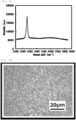
- Figs. 3A and 3B show the results in an optional part. As shown in Fig. 3A , the growth of diamond was confirmed. In addition, as shown in Fig. 3B , high crystallinity was observed.
- Example 1 substrate on which diamond was grown
- the substrate of Example 1 was placed in a hot filament apparatus and grown under the following conditions: filament temperature of 2200°C, H 2 flow rate of 10 SLM, CH 4 concentration of 3%, substrate temperature of 850°C, and 5 Torr for 4 hours.
- the thickness of the large-diameter diamond layer could be increased.
- Figs. 4A and 4B show the results in an optional part. As shown in Fig. 4A , the growth of diamond was confirmed. In addition, as shown in Fig. 4B , high crystallinity was observed.
- a large-diameter diamond layer with high crystallinity could be formed.
Landscapes
- Chemical & Material Sciences (AREA)
- Engineering & Computer Science (AREA)
- Metallurgy (AREA)
- Materials Engineering (AREA)
- Organic Chemistry (AREA)
- Chemical Kinetics & Catalysis (AREA)
- General Chemical & Material Sciences (AREA)
- Mechanical Engineering (AREA)
- Crystallography & Structural Chemistry (AREA)
- Inorganic Chemistry (AREA)
- Physics & Mathematics (AREA)
- Plasma & Fusion (AREA)
- Crystals, And After-Treatments Of Crystals (AREA)
Abstract
The present invention is a method for growing a diamond layer by a microwave plasma CVD method, including: a step of placing a substrate 2 in a reaction vessel 1 of a microwave plasma CVD apparatus 10; a step of introducing a raw material gas (reaction gas) 6 into the reaction vessel 1; and a step of growing a diamond layer on a surface of the substrate 2 by irradiating microwave plasma on the surface of the substrate 2, wherein the step of growing the diamond layer includes at least one of moving the substrate 2 in a direction parallel to the surface of the substrate 2 and moving an irradiation position of the microwave plasma in a direction parallel to the surface of the substrate 2. Thereby, a large-diameter diamond substrate is provided.
Description
- The present invention relates to a method for growing a diamond layer and a microwave plasma CVD apparatus. In particular, the present invention relates to technology regarding artificial diamond growth on a semiconductor substrate. More particularly, the present invention relates to a method for growing diamond and an apparatus thereof in growing diamond by CVD (chemical vapor deposition method) on a silicon substrate.
- Diamond has been expected to be applied to various semiconductor devices and electronic devices because of having excellent physical property values such as high hardness, preferable thermal conductivity, high carrier mobility, and having a wide bandgap. Artificially synthesized diamond is used in the semiconductor device and electronic device applications. There are two methods for synthesizing diamond, that is, a growth method using ultrahigh pressure, and a vapor phase growth method. The vapor phase growth (CVD growth) has attracted attention in application to semiconductors, because a large diameter can be obtained (
Patent Documents 1 to 3). -
- Patent Document 1:
JP 2001-354491 A - Patent Document 2:
JP 2004-176132 A - Patent Document 3:
JP 2006-143561 A - The CVD growth is a method including placing a substrate inside a reaction tube, flowing a raw material gas (reaction gas) and carrier gas under normal pressure or reduced pressure, decomposing or activating the raw material gas (reaction gas) by thermal decomposition or plasma, and thereby causing growth on the substrate.
- In diamond, microwave plasma, DC plasma, or a hot filament method using a filament such as tungsten is employed. In single crystal growth, the microwave plasma method has attracted attention. Microwave plasma growth is a method including irradiating microwave to a substrate, decomposing or activating a raw material gas (reaction gas), and thereby growing single crystal diamond.
-
Fig. 5 is a diagram illustrating a conventional microwave plasma CVD apparatus. - As shown in
Fig. 5 , a conventional microwaveplasma CVD apparatus 110 has areaction vessel 101, inside of which a silicon substrate (substrate to be film-formed) 102 can be placed. Inside of thereaction vessel 101 can be depressurized. - On the wall, a reaction
gas introduction tube 109 is attached, and areaction gas 106 can be introduced therein. Thereaction gas 106 is, for example, a gas mixture of hydrogen gas and methane gas. - On the ceiling, a
microwave introduction tube 104 connected to a microwave generator 105 (2.45 GHz) is attached. Themicrowave introduction tube 104 can irradiate microwave plasma toward the direct downward direction. - On the bottom surface side, a plate-shaped stage 103 (for heating substrate) is placed. The surface of the
stage 103 is in parallel to the direction perpendicular to the above direct downward direction. Additionally, asilicon substrate 102 can be placed on the surface of thestage 103. - A
silicon substrate 102 is placed on the surface of thestage 103. - As can be seen in
Fig. 5 , in principle, the area that can be irradiated by microwave is limited. Thus, the substrate diameter is limited. - A diamond substrate has attracted attention in view of the heat dissipation characteristics, or the like. Although the growth method applicable to single crystal substrates is microwave plasma growth, it has not been possible to achieve a large diameter such as 300 mm φ due to the limitation of the area that can be irradiated by microwave.
- Thus, formation of a large-diameter diamond substrate has been needed.
- The present invention has been made to solve the problem described above, and has an object to provide a method for growing a diamond layer and a microwave plasma CVD apparatus that can achieve a large diameter.
- The present invention has been made to achieve the above object, and provides a method for growing a diamond layer by a microwave plasma CVD method, including: a step of placing a substrate in a reaction vessel of a microwave plasma CVD apparatus; a step of introducing a raw material gas (reaction gas) into the reaction vessel; and a step of growing a diamond layer on a surface of the substrate by irradiating microwave plasma on the surface of the substrate, wherein the step of growing the diamond layer includes at least one of moving the substrate in a direction parallel to the surface of the substrate and moving an irradiation position of the microwave plasma in a direction parallel to the surface of the substrate.
- According to the method for growing a diamond layer as described above, a large-diameter diamond layer can be formed. In more detail, in growing diamond on a large-diameter silicon substrate, the growth can be caused by placing a large-diameter silicon substrate on a stage of a microwave plasma growth apparatus, and introducing a raw material gas (reaction gas) while irradiating microwave to the substrate and moving the stage for each predetermined time. Thus, it is possible to grow a large-diameter single crystal diamond layer even with a microwave plasma CVD apparatus. Furthermore, by laterally growing the diamond layer in a part with high plasma density, and by promoting horizontal growth in a part with low plasma density, the method can also contribute to reduction of defects.
- Note that it is defined that at least one of moving the substrate in a direction parallel to the surface of the substrate and moving an irradiation position of the microwave plasma in a direction parallel to the surface of the substrate is performed. Accordingly, the substrate may be moved after securing the plasma irradiation position, or on the contrary, the microwave plasma irradiation position (where microwave plasma density is high) may be moved in X and Y direction after securing the substrate, or both the substrate and irradiation position may be moved. By either method, it is possible to grow a large diameter single crystal diamond.
- In this case, the method for growing a diamond layer described above can include that diamond is further grown on the diamond layer by a hot filament CVD method after transferring the substrate on which the diamond layer is grown into a reaction vessel of a hot filament CVD apparatus, after the step of growing the diamond layer.
- Thereby, the thickness of the large-diameter diamond layer can be increased. By further growing the substrate grown by the microwave plasma CVD method using a hot filament CVD apparatus capable of causing large-diameter growth, further thick diamond can be grown on a large-diameter substrate. The diamond film grown by the microwave plasma CVD method may be used as it is. But for growing the diamond film thicker, more specifically, rather than the growth is caused by microwave plasma alone, the substrate grown by microwave plasma with the above method may be placed in a diamond growth apparatus using a hot filament method, methane and hydrogen may be introduced as gas into the reaction vessel, and the gas may be electrically heated and decomposed by energizing a filament such as tungsten provided above the substrate to grow diamond on the substrate. Thus, diamond can be grown on the entire large-diameter substrate.
- In this case, the method for growing a diamond layer described above can include that a silicon substrate is used as the substrate.
- Thereby, when an integrated circuit is formed on the silicon substrate on which a diamond layer has been formed, the diamond layer can be used as a heat sink layer.
- Moreover, the present invention provides a microwave plasma CVD apparatus used for a method for growing a diamond layer, including at least one of a mechanism for moving a substrate in a direction parallel to a surface of the substrate and a mechanism for moving an irradiation position of microwave plasma.
- By using the microwave plasma CVD apparatus described above, it is possible to form a large-diameter diamond layer. More particularly, if the apparatus has this mechanism, it is possible to grow large-diameter single crystal diamond even with the microwave plasma CVD apparatus.
- In this case, the microwave plasma CVD apparatus described above can further include a mechanism for heating a substrate.
- Thereby, growth of the large-diameter diamond layer can be promoted.
- As described above, according to the method for growing a diamond layer of the present invention, it is possible to form a large-diameter diamond layer by a microwave plasma CVD method. In particular, in the present invention, it is possible to grow a single crystal large-diameter diamond layer by a microwave plasma CVD method.
- Also, according to the microwave plasma CVD apparatus of the present invention, it is possible to form a large-diameter diamond layer.
-
-
Fig. 1 is a diagram illustrating a microwave plasma CVD apparatus of the present invention; -
Fig. 2 is a diagram illustrating a hot filament CVD apparatus used for the method for growing a diamond layer of the present invention; -
Fig. 3A is a graph showing Raman peak of a diamond film grown by the method for growing a diamond layer of the present invention (by a microwave plasma method alone); -
Fig. 3B is an optical microscope image of a surface of a diamond film grown by the method for growing a diamond layer of the present invention (by a microwave plasma method alone); -
Fig. 4A is a graph showing Raman peak of a diamond film grown by the method for growing a diamond layer of the present invention (by a microwave plasma method and hot filament method); -
Fig. 4B is an optical microscope image of a surface of a diamond film grown by the method for growing a diamond layer of the present invention (by a microwave plasma method and hot filament method); and -
Fig. 5 is a diagram illustrating a conventional microwave plasma CVD apparatus. - Hereinafter, the present invention will be described in detail. However, the present invention is not limited thereto.
- As described above, it has been required to provide a method for growing a diamond layer and a microwave plasma CVD apparatus that can form a large-diameter diamond layer, in particular a single crystal diamond layer, on a large-diameter silicon substrate.
- The present inventors made intensive investigations on the above problem. As a result, they found that a large-diameter diamond layer, in particular a single crystal diamond layer can be formed on a large-diameter silicon substrate by a method for growing a diamond layer by a microwave plasma CVD method, including: a step of placing a substrate in a reaction vessel of a microwave plasma CVD apparatus; a step of introducing a raw material gas (reaction gas) into the reaction vessel; and a step of growing a diamond layer on a surface of the substrate by irradiating microwave plasma on the surface of the substrate, wherein the step of growing the diamond layer includes at least one of moving the substrate in a direction parallel to the surface of the substrate and moving an irradiation position of the microwave plasma in a direction parallel to the surface of the substrate. Thus, they completed the present invention.
- Hereinafter, the method for growing a diamond layer and the microwave plasma CVD apparatus according to a first embodiment of the present invention will be described with referring to
Fig. 1 . -
Fig. 1 is a diagram illustrating the microwave plasma CVD apparatus of the present invention. - As shown in
Fig. 1 , a microwaveplasma CVD apparatus 10 of the present invention has areaction vessel 1, inside of which a large-diameter silicon substrate 2 can be placed. Thereaction vessel 1 is approximately circular in plan view. However, the shape of thereaction vessel 1 is not limited thereto, and may be approximately rectangular in plan view. Inside of thereaction vessel 1 can be depressurized. - Note that the left-right direction of the paper surface is X direction, and the direction perpendicular to the paper surface is Y direction.
- On the wall, a reaction gas introduction tube 9 is attached, and a
reaction gas 6 can be introduced therein. Thereaction gas 6 is, for example, a gas mixture of hydrogen gas and methane gas. - On the ceiling, a
microwave introduction tube 4 connected to a microwave generator 5 (2.45 GHz) is attached. Themicrowave introduction tube 4 can irradiate microwave plasma toward the direct downward direction. - On the bottom surface side, a plate-shaped stage 7 (for heating substrate, movable in X and Y direction) is placed. The surface of the stage 7 is in parallel to the direction perpendicular to the above direct downward direction. Additionally, the large-
diameter silicon substrate 2 can be placed on the surface of the stage 7. Furthermore, the stage 7 includes a mechanism movable in the X and Y direction, and a mechanism capable of heating the large-diameter silicon substrate (substrate to be film-formed) 2 that is placed on the surface of the stage 7. - The large-
diameter silicon substrate 2 is placed on the surface of the stage 7. - The large-
diameter silicon substrate 2 is prepared by, for example, providing a boron-doped high-resistivity single crystal (111) silicon substrate with a 300 mm diameter, polishing the substrate surface with a #8000 grindstone (average particle size of abrasive grain: 2 to 4 µm), thereby roughening the silicon surface to introduce damage, and producing a nucleus for diamond growth. - Next, the method for growing a diamond layer is described.
- The method for growing a diamond layer of the present invention is a method for growing a diamond layer, in particular a single crystal diamond layer, by a microwave plasma CVD method.
- The method includes: a step of placing a substrate in a reaction vessel of a microwave plasma CVD apparatus (substrate placement step); a step of introducing a raw material gas (reaction gas) into the reaction vessel (raw material gas (reaction gas) introduction step); and a step of growing a diamond layer on the surface of the substrate by irradiating microwave plasma on the surface of the substrate (diamond layer growth step).
- At first, as shown in
Fig. 1 , on the surface of the plate-shaped stage 7 placed on the bottom surface side of thereaction vessel 1 of the microwaveplasma CVD apparatus 10, the large-diameter silicon substrate 2 is placed. - Next, the inside of the
reaction vessel 1 is depressurized, and then thereaction gas 6 is introduced therein through the reaction gas introduction tube 9. - Next, a diamond layer is grown on the surface of the large-
diameter silicon substrate 2 by irradiating microwave plasma on the surface of the large-diameter silicon substrate 2. - The growing of the diamond layer includes at least one of moving the large-
diameter silicon substrate 2 in a direction parallel to the surface of the large-diameter silicon substrate 2 and moving an irradiation position of the microwave plasma in a direction parallel to the surface of the substrate. Thereby, microwave plasma generated locally can be uniformly irradiated on the surface of the large-diameter silicon substrate, so that a large-diameter diamond layer can be uniformly formed on the surface of the large-diameter silicon substrate. - "Moving in a direction parallel to the surface of the substrate" includes rotary movement such as rotation and revolution as well as parallel movement of the substrate in the X-Y direction.
- The moving speed is, for example, preferably about 1 to 50 mm/min when the substrate is moved in parallel to the X-Y direction, and in the case of rotary movement, it is preferably about 1 to 100 rpm.
- In addition, when growing the diamond layer, it is preferable to heat the large-
diameter silicon substrate 2. Thereby, the growth can be promoted. - Evaluation of the diamond layer is carried out by, for example, Raman measurement, optical microscope image observation of the surface, X-ray diffraction, or the like, in a plurality of parts of the large-diameter diamond layer surface. It is possible to determine the crystallinity of the large-diameter diamond layer or whether the layer surface is uniform.
- At first, the hot filament CVD apparatus used in the method for growing a diamond layer in the second embodiment of the present invention is described with referring to
Fig. 2 . -
Fig. 2 is a diagram illustrating a hot filament CVD apparatus used for the method for growing a diamond layer of the present invention. - As shown in
Fig. 2 , a hotfilament CVD apparatus 20 used for the method for growing a diamond layer of the present invention has thereaction vessel 1, inside of which the large-diameter silicon substrate 2 having a thin diamond layer formed on the surface, can be placed. Inside of thereaction vessel 1 can be depressurized. - On the ceiling, the reaction gas introduction tube 9 is attached, and the
reaction gas 6 can be introduced therein. Thereaction gas 6 is, for example, a gas mixture of hydrogen gas and methane gas. - A
linear filament 8 is attached separated from the lower part of the ceiling directly below the reaction gas introduction tube 9 so as to be parallel to the lower surface of the ceiling. - Heating temperature of the
filament 8 is, for example, 2200°C. For example, thefilament 8 is made of, but not limited to, tungsten. The shape of the filament is not limited to linear, but may be a net shape. - Next, the method for growing a diamond layer according to the second embodiment is described.
- The method for growing a diamond layer according to the second embodiment is a method for further growing a diamond layer on the diamond layer formed by the method for growing a diamond layer according to the first embodiment with a hot filament CVD apparatus.
- That is, the method for growing a diamond layer according to the second embodiment includes a substrate placement step, a raw material gas (reaction gas) introduction step, and a step of growing a diamond layer in the method for growing a diamond layer according to the first embodiment, and additionally, a step of placing a substrate in a reaction vessel of a hot filament CVD apparatus (substrate placement step) and a step of further growing a diamond layer with the hot filament CVD apparatus (diamond layer additional growth step).
- The large-
diameter silicon substrate 2 on the surface of which a diamond layer, in particular a single crystal diamond layer, is formed thinly by the method for growing a diamond layer according to the first embodiment is placed in a reaction vessel of the hot filament CVD apparatus with the diamond layer facing toward the ceiling. - After depressurizing the inside of the
reaction vessel 1, thefilament 8 is heated to a predetermined temperature. - Thereafter, from the reaction gas introduction tube 9, the
reaction gas 6 composed of a gas mixture of hydrogen gas and methane gas is introduced therein. - The
linear filament 8 is attached separated from the lower part of the ceiling, directly below the reaction gas introduction tube 9 so as to be parallel to the lower surface of the ceiling. Thereby, thereaction gas 6 ejected from the reaction gas introduction tube 9 is heated by thefilament 8, and collides with a thin diamond layer formed on the surface of the large-diameter silicon substrate 2. An additional diamond layer can be grown accordingly. - Hereinafter, the present invention will be specifically described with reference to Examples. However, the present invention is not limited thereto.
- A boron-doped high-resistivity single crystal (111) silicon substrate with a 300 mm diameter was provided. Then, the surface of the substrate was polished with a #8000 grindstone (average particle size of abrasive grain: 2 to 4 µm) to roughen the silicon surface for introducing damage, and thereby producing a nucleus for diamond growth.
- This substrate was introduced into a microwave plasma growth apparatus, and 2.45 GHz microwave was irradiated under the following conditions: 1500 W, H2 flow rate of 10 SLM, CH4 concentration of 3%, substrate temperature of 850°C, and 60 Torr. Then, while moving the irradiation position at a speed of 10 mm/min, thereby causing the growth.
- As a result, a large-diameter diamond layer could be formed.
- Thereafter, Raman measurement and optical microscope image observation of the surface were performed in a plurality of parts of the large-diameter diamond layer surface.
-
Figs. 3A and 3B show the results in an optional part. As shown inFig. 3A , the growth of diamond was confirmed. In addition, as shown inFig. 3B , high crystallinity was observed. - That is, in any parts, the Raman peak was confirmed, and the optical microscope image of the surface could be observed.
- The substrate of Example 1 (substrate on which diamond was grown) was placed in a hot filament apparatus and grown under the following conditions: filament temperature of 2200°C, H2 flow rate of 10 SLM, CH4 concentration of 3%, substrate temperature of 850°C, and 5 Torr for 4 hours.
- As a result, the thickness of the large-diameter diamond layer could be increased.
- Thereafter, Raman measurement and optical microscope image observation of the surface were performed in a plurality of parts of the large-diameter diamond layer surface.
-
Figs. 4A and 4B show the results in an optional part. As shown inFig. 4A , the growth of diamond was confirmed. In addition, as shown inFig. 4B , high crystallinity was observed. - That is, in any parts, the Raman peak was confirmed, and the optical microscope image of the surface could be observed.
- As described above, according to the Examples of the present invention, a large-diameter diamond layer with high crystallinity could be formed.
- It should be noted that the present invention is not limited to the above-described embodiments. The embodiments are just examples, and any examples that substantially have the same feature and demonstrate the same functions and effects as those in the technical concept disclosed in claims of the present invention are included in the technical scope of the present invention.
Claims (5)
- A method for growing a diamond layer by a microwave plasma CVD method, comprising:a step of placing a substrate in a reaction vessel of a microwave plasma CVD apparatus;a step of introducing a raw material gas (reaction gas) into the reaction vessel; anda step of growing a diamond layer on a surface of the substrate by irradiating microwave plasma on the surface of the substrate, whereinthe step of growing the diamond layer comprises at least one of moving the substrate in a direction parallel to the surface of the substrate and moving an irradiation position of the microwave plasma in a direction parallel to the surface of the substrate.
- The method for growing a diamond layer according to claim 1, wherein diamond is further grown on the diamond layer by a hot filament CVD method after transferring the substrate on which the diamond layer is grown into a reaction vessel of a hot filament CVD apparatus, after the step of growing the diamond layer.
- The method for growing a diamond layer according to claim 1 or 2, wherein a silicon substrate is used as the substrate.
- A microwave plasma CVD apparatus used for a method for growing a diamond layer, comprising at least one of a mechanism for moving a substrate in a direction parallel to a surface of the substrate and a mechanism for moving an irradiation position of microwave plasma.
- The microwave plasma CVD apparatus according to claim 4, further comprising a mechanism for heating a substrate.
Applications Claiming Priority (2)
| Application Number | Priority Date | Filing Date | Title |
|---|---|---|---|
| JP2022102056 | 2022-06-24 | ||
| PCT/JP2023/017217 WO2023248626A1 (en) | 2022-06-24 | 2023-05-08 | Method for growing diamond layer, and microwave plasma cvd device |
Publications (1)
| Publication Number | Publication Date |
|---|---|
| EP4545692A1 true EP4545692A1 (en) | 2025-04-30 |
Family
ID=89379540
Family Applications (1)
| Application Number | Title | Priority Date | Filing Date |
|---|---|---|---|
| EP23826815.5A Pending EP4545692A1 (en) | 2022-06-24 | 2023-05-08 | Method for growing diamond layer, and microwave plasma cvd device |
Country Status (7)
| Country | Link |
|---|---|
| US (1) | US20250369103A1 (en) |
| EP (1) | EP4545692A1 (en) |
| JP (1) | JPWO2023248626A1 (en) |
| KR (1) | KR20250026188A (en) |
| CN (1) | CN119365636A (en) |
| TW (1) | TW202401526A (en) |
| WO (1) | WO2023248626A1 (en) |
Family Cites Families (10)
| Publication number | Priority date | Publication date | Assignee | Title |
|---|---|---|---|---|
| CA2054050C (en) * | 1990-11-16 | 1998-07-07 | Louis K. Bigelow | Method and apparatus for making grit and abrasive media |
| JPH0517290A (en) * | 1991-07-12 | 1993-01-26 | Japan Steel Works Ltd:The | Method and apparatus for synthesizing diamond |
| JPH05239655A (en) * | 1991-12-06 | 1993-09-17 | Denki Kogyo Co Ltd | Diamond film synthesizer by microwave plasma CVD method |
| US5387288A (en) * | 1993-05-14 | 1995-02-07 | Modular Process Technology Corp. | Apparatus for depositing diamond and refractory materials comprising rotating antenna |
| JP3621730B2 (en) * | 1994-11-02 | 2005-02-16 | 三菱重工業株式会社 | Microwave plasma chemical vapor deposition system |
| US5643365A (en) * | 1996-07-25 | 1997-07-01 | Ceram Optec Industries Inc | Method and device for plasma vapor chemical deposition of homogeneous films on large flat surfaces |
| JP2001354491A (en) | 2000-06-07 | 2001-12-25 | New Japan Radio Co Ltd | Method and device for growing diamond |
| JP2004176132A (en) | 2002-11-27 | 2004-06-24 | Toppan Printing Co Ltd | Nanodiamond film and method of manufacturing the same |
| JP2006143561A (en) | 2004-11-24 | 2006-06-08 | Japan Science & Technology Agency | Low temperature synthesis method of diamond |
| CN111850506B (en) * | 2020-07-07 | 2022-06-17 | 武汉大学深圳研究院 | Device and method for preparing n-type doped diamond by microwave plasma-hot wire composite chemical vapor deposition |
-
2023
- 2023-05-08 KR KR1020247042061A patent/KR20250026188A/en active Pending
- 2023-05-08 EP EP23826815.5A patent/EP4545692A1/en active Pending
- 2023-05-08 CN CN202380046789.1A patent/CN119365636A/en active Pending
- 2023-05-08 JP JP2024528370A patent/JPWO2023248626A1/ja active Pending
- 2023-05-08 US US18/876,870 patent/US20250369103A1/en active Pending
- 2023-05-08 WO PCT/JP2023/017217 patent/WO2023248626A1/en not_active Ceased
- 2023-05-09 TW TW112117066A patent/TW202401526A/en unknown
Also Published As
| Publication number | Publication date |
|---|---|
| TW202401526A (en) | 2024-01-01 |
| WO2023248626A1 (en) | 2023-12-28 |
| CN119365636A (en) | 2025-01-24 |
| US20250369103A1 (en) | 2025-12-04 |
| JPWO2023248626A1 (en) | 2023-12-28 |
| KR20250026188A (en) | 2025-02-25 |
Similar Documents
| Publication | Publication Date | Title |
|---|---|---|
| Schreck et al. | Ion bombardment induced buried lateral growth: the key mechanism for the synthesis of single crystal diamond wafers | |
| CN102102220B (en) | Preparation method of graphene on diamond (111) surface | |
| US7776408B2 (en) | Method and apparatus for producing single crystalline diamonds | |
| Bansal et al. | Substrate modification during chemical vapor deposition of hBN on sapphire | |
| KR20100035161A (en) | Diamond film deposition | |
| JP2603257B2 (en) | Diamond multilayer thin film | |
| Drijkoningen et al. | On the origin of diamond plates deposited at low temperature | |
| Alcantar-Peña et al. | Fundamentals towards large area synthesis of multifunctional Ultrananocrystalline diamond films via large area hot filament chemical vapor deposition bias enhanced nucleation/bias enhanced growth for fabrication of broad range of multifunctional devices | |
| JP2013067549A (en) | Method for forming thin film | |
| KC et al. | Effect of seeding density on the growth of diamond films by hot-filament chemical vapor deposition from sparse to dense range | |
| JP7831490B2 (en) | Method for manufacturing heteroepitaxial wafers | |
| Baudrillart et al. | Microstructure and growth kinetics of nanocrystalline diamond films deposited in large area/low temperature distributed antenna array microwave‐plasma reactor | |
| KR102314020B1 (en) | METHOD OF MAUFACTURING OF HEXAGONAL BORON NITRIDE (h-BN)/GRAPHENE IN-PLANE HETEROSTRUCTURE | |
| US20250369103A1 (en) | Method for growing diamond layer and microwave plasma cvd apparatus | |
| Sanchez et al. | Low-temperature growth of epitaxial β-SiC on Si (100) using supersonic molecular beams of methylsilane | |
| RU2522812C1 (en) | Method of manufacturing products, containing silicon substrate with silicon carbide film on its surface and reactor of realising thereof | |
| JP6783722B2 (en) | Boron Nitride Film Growth Device and Method | |
| WO2008035468A1 (en) | THIN NANODIAMOND FILM HAVING n-TYPE CONDUCTIVITY AND PROCESS FOR PRODUCING THE SAME | |
| JP3185289B2 (en) | Diamond deposition method | |
| TW202336256A (en) | Vapor-phase precursor seeding for diamond film deposition | |
| KR20030074183A (en) | A substrate for forming chemical vapor-deposited diamond film and a diamond film | |
| JP3124422B2 (en) | Method of forming highly oriented diamond thin film | |
| Wang et al. | Interface study of diamond films grown on (100) silicon | |
| KR102401334B1 (en) | A method for bandgap engineering of diamond by hybridization with graphene | |
| Ali et al. | Effect of surface treatment on hot-filament chemical vapour deposition grown diamond films |
Legal Events
| Date | Code | Title | Description |
|---|---|---|---|
| STAA | Information on the status of an ep patent application or granted ep patent |
Free format text: STATUS: THE INTERNATIONAL PUBLICATION HAS BEEN MADE |
|
| PUAI | Public reference made under article 153(3) epc to a published international application that has entered the european phase |
Free format text: ORIGINAL CODE: 0009012 |
|
| STAA | Information on the status of an ep patent application or granted ep patent |
Free format text: STATUS: REQUEST FOR EXAMINATION WAS MADE |
|
| 17P | Request for examination filed |
Effective date: 20241212 |
|
| AK | Designated contracting states |
Kind code of ref document: A1 Designated state(s): AL AT BE BG CH CY CZ DE DK EE ES FI FR GB GR HR HU IE IS IT LI LT LU LV MC ME MK MT NL NO PL PT RO RS SE SI SK SM TR |
|
| DAV | Request for validation of the european patent (deleted) | ||
| DAX | Request for extension of the european patent (deleted) |