EP4545691A1 - SIC epitaxial wafer - Google Patents
SIC epitaxial wafer Download PDFInfo
- Publication number
- EP4545691A1 EP4545691A1 EP24207314.6A EP24207314A EP4545691A1 EP 4545691 A1 EP4545691 A1 EP 4545691A1 EP 24207314 A EP24207314 A EP 24207314A EP 4545691 A1 EP4545691 A1 EP 4545691A1
- Authority
- EP
- European Patent Office
- Prior art keywords
- sic epitaxial
- stacking faults
- sic
- density
- epitaxial wafer
- Prior art date
- Legal status (The legal status is an assumption and is not a legal conclusion. Google has not performed a legal analysis and makes no representation as to the accuracy of the status listed.)
- Pending
Links
Images
Classifications
-
- C—CHEMISTRY; METALLURGY
- C30—CRYSTAL GROWTH
- C30B—SINGLE-CRYSTAL GROWTH; UNIDIRECTIONAL SOLIDIFICATION OF EUTECTIC MATERIAL OR UNIDIRECTIONAL DEMIXING OF EUTECTOID MATERIAL; REFINING BY ZONE-MELTING OF MATERIAL; PRODUCTION OF A HOMOGENEOUS POLYCRYSTALLINE MATERIAL WITH DEFINED STRUCTURE; SINGLE CRYSTALS OR HOMOGENEOUS POLYCRYSTALLINE MATERIAL WITH DEFINED STRUCTURE; AFTER-TREATMENT OF SINGLE CRYSTALS OR A HOMOGENEOUS POLYCRYSTALLINE MATERIAL WITH DEFINED STRUCTURE; APPARATUS THEREFOR
- C30B29/00—Single crystals or homogeneous polycrystalline material with defined structure characterised by the material or by their shape
- C30B29/10—Inorganic compounds or compositions
- C30B29/36—Carbides
-
- H—ELECTRICITY
- H10—SEMICONDUCTOR DEVICES; ELECTRIC SOLID-STATE DEVICES NOT OTHERWISE PROVIDED FOR
- H10D—INORGANIC ELECTRIC SEMICONDUCTOR DEVICES
- H10D62/00—Semiconductor bodies, or regions thereof, of devices having potential barriers
- H10D62/50—Physical imperfections
- H10D62/57—Physical imperfections the imperfections being on the surface of the semiconductor body, e.g. the body having a roughened surface
-
- C—CHEMISTRY; METALLURGY
- C30—CRYSTAL GROWTH
- C30B—SINGLE-CRYSTAL GROWTH; UNIDIRECTIONAL SOLIDIFICATION OF EUTECTIC MATERIAL OR UNIDIRECTIONAL DEMIXING OF EUTECTOID MATERIAL; REFINING BY ZONE-MELTING OF MATERIAL; PRODUCTION OF A HOMOGENEOUS POLYCRYSTALLINE MATERIAL WITH DEFINED STRUCTURE; SINGLE CRYSTALS OR HOMOGENEOUS POLYCRYSTALLINE MATERIAL WITH DEFINED STRUCTURE; AFTER-TREATMENT OF SINGLE CRYSTALS OR A HOMOGENEOUS POLYCRYSTALLINE MATERIAL WITH DEFINED STRUCTURE; APPARATUS THEREFOR
- C30B23/00—Single-crystal growth by condensing evaporated or sublimed materials
- C30B23/02—Epitaxial-layer growth
-
- H—ELECTRICITY
- H10—SEMICONDUCTOR DEVICES; ELECTRIC SOLID-STATE DEVICES NOT OTHERWISE PROVIDED FOR
- H10D—INORGANIC ELECTRIC SEMICONDUCTOR DEVICES
- H10D62/00—Semiconductor bodies, or regions thereof, of devices having potential barriers
- H10D62/50—Physical imperfections
- H10D62/53—Physical imperfections the imperfections being within the semiconductor body
-
- H—ELECTRICITY
- H10—SEMICONDUCTOR DEVICES; ELECTRIC SOLID-STATE DEVICES NOT OTHERWISE PROVIDED FOR
- H10D—INORGANIC ELECTRIC SEMICONDUCTOR DEVICES
- H10D62/00—Semiconductor bodies, or regions thereof, of devices having potential barriers
- H10D62/80—Semiconductor bodies, or regions thereof, of devices having potential barriers characterised by the materials
- H10D62/83—Semiconductor bodies, or regions thereof, of devices having potential barriers characterised by the materials being Group IV materials, e.g. B-doped Si or undoped Ge
- H10D62/832—Semiconductor bodies, or regions thereof, of devices having potential barriers characterised by the materials being Group IV materials, e.g. B-doped Si or undoped Ge being Group IV materials comprising two or more elements, e.g. SiGe
- H10D62/8325—Silicon carbide
-
- H—ELECTRICITY
- H10—SEMICONDUCTOR DEVICES; ELECTRIC SOLID-STATE DEVICES NOT OTHERWISE PROVIDED FOR
- H10P—GENERIC PROCESSES OR APPARATUS FOR THE MANUFACTURE OR TREATMENT OF DEVICES COVERED BY CLASS H10
- H10P14/00—Formation of materials, e.g. in the shape of layers or pillars
- H10P14/20—Formation of materials, e.g. in the shape of layers or pillars of semiconductor materials
- H10P14/29—Formation of materials, e.g. in the shape of layers or pillars of semiconductor materials characterised by the substrates
- H10P14/2901—Materials
- H10P14/2902—Materials being Group IVA materials
- H10P14/2904—Silicon carbide
-
- H—ELECTRICITY
- H10—SEMICONDUCTOR DEVICES; ELECTRIC SOLID-STATE DEVICES NOT OTHERWISE PROVIDED FOR
- H10P—GENERIC PROCESSES OR APPARATUS FOR THE MANUFACTURE OR TREATMENT OF DEVICES COVERED BY CLASS H10
- H10P14/00—Formation of materials, e.g. in the shape of layers or pillars
- H10P14/20—Formation of materials, e.g. in the shape of layers or pillars of semiconductor materials
- H10P14/34—Deposited materials, e.g. layers
- H10P14/3402—Deposited materials, e.g. layers characterised by the chemical composition
- H10P14/3404—Deposited materials, e.g. layers characterised by the chemical composition being Group IVA materials
- H10P14/3408—Silicon carbide
Definitions
- the present disclosure relates to a SiC epitaxial wafer.
- Silicon carbide (SiC) has a dielectric breakdown field one order of magnitude larger and a band gap three times larger than silicon (Si).
- silicon carbide (SiC) has properties such as a thermal conductivity about three times higher than silicon (Si). For this reason, silicon carbide (SiC) is expected to be applied to power devices, high frequency devices, high temperature operating devices, and the like. For this reason, in recent years, SiC epitaxial wafers have come to be used for the above-described semiconductor devices.
- a SiC epitaxial wafer is obtained by stacking a SiC epitaxial layer on the surface of a SiC substrate.
- the substrate before the SiC epitaxial layer is stacked thereon is referred to as a SiC substrate
- the substrate after the SiC epitaxial layer is stacked thereon is referred to as a SiC epitaxial wafer.
- the SiC substrate is produced by being cut out from a SiC ingot.
- SiC devices such as power devices, high frequency devices, and high temperature operating devices are obtained by forming devices in a SiC epitaxial layer of a SiC epitaxial wafer and then cutting the SiC epitaxial wafer into chips.
- the SiC epitaxial wafer contains inherent crystal defects. Some crystal defects adversely affect subsequent processes and hinder normal operation of the SiC devices. Such defects are called killer defects. For example, it is known that basal plane dislocations (BPDs) cause stacking faults which are one type of killer defect (see, for example, Patent Document 1).
- BPDs basal plane dislocations
- Patent Document 2 discloses a case in which there are a plurality of types of stacking faults and a method for reducing the total number of stacking faults and double Shockley type stacking faults among them.
- BPDs basal plane dislocations
- the present disclosure has been made in consideration of the above problems, and an object of the present disclosure is to provide a SiC epitaxial wafer in which it possible to estimate a position at which many basal plane dislocations are concentrated and the number of basal plane dislocations in a SiC substrate even after a SiC epitaxial layer is stacked.
- the SiC epitaxial wafer according to the above aspect it possible to estimate the position at which many basal plane dislocations are concentrated and the number of basal plane dislocations in a SiC substrate even after a SiC epitaxial layer is stacked.
- an individual orientation is indicated by [ ] and a collective orientation is indicated by ⁇ >.
- a "-" is customarily placed above the number in crystallography, but in the present specification, a negative sign is placed before the number.
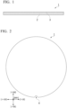
- FIG. 1 is a cross-sectional view of a SiC epitaxial wafer 1 according to the present embodiment.
- FIG. 2 is a plan view of the SiC epitaxial wafer 1 according to the present embodiment.
- the SiC epitaxial wafer 1 includes a SiC substrate 2 and a SiC epitaxial layer 3.
- the shape of the SiC epitaxial wafer 1 in a plan view is approximately circular.
- the SiC epitaxial wafer 1 may have a notch 4 for checking the direction of a crystal axis.
- the SiC substrate 2 may have an orientation flat instead of the notch 4.
- the diameter of the SiC epitaxial wafer 1 is, for example, 145 mm or more, and preferably 149 mm or more. In addition, the diameter of the SiC epitaxial wafer 1 is preferably 155 mm or less, and more preferably 151 mm or less. In addition, the diameter of the SiC epitaxial wafer 1 may be, for example, 195 mm or more, and preferably 199 mm or more. In addition, the diameter of the SiC epitaxial wafer 1 is preferably 205 mm or less, and more preferably 201 mm or less.
- the SiC substrate 2 is made of, for example, n-type SiC.
- the polytype of the SiC substrate 2 is not particularly limited and may be any of 2H, 3C, 4H, and 6H.
- the SiC substrate 2 is, for example, 4H-SiC.
- the density of basal plane dislocations is 1/cm 2 or more and 3000/cm 2 or less.
- the basal plane dislocations in the SiC substrate 2 are taken over by the SiC epitaxial layer 3, stacking faults which are one type of killer defect may be caused. For this reason, it is ideal that there be no basal plane dislocations in the SiC substrate 2.
- the density of the basal plane dislocations is within a desired range, it is possible to relatively stably produce the SiC substrate 2. In other words, if the density of the basal plane dislocations is 1/cm 2 or more and 3000/cm 2 or less, it is possible to stably obtain the SiC substrate 2 while satisfying the required quality.
- the SiC epitaxial wafer 1 it possible to estimate the position at which many basal plane dislocations are concentrated and the number of basal plane dislocations in a SiC substrate 2 after the SiC epitaxial layer 3 is stacked, and thus it is not necessary to constantly measure the density of the basal plane dislocations in the SiC substrate 2.
- it becomes necessary to evaluate the density of the basal plane dislocations in the SiC substrate 2 it is possible to measure the density of the basal plane dislocations using a photoluminescence method, for example.
- the SiC epitaxial layer 3 is stacked on one surface of the SiC substrate 2.
- the density of double Shockley (2SSF) type stacking faults is 4/cm 2 or more and 10/cm 2 or less.
- the density of the double Shockley (2SSF) type stacking faults is more preferably 6/cm 2 or more and 10/cm 2 or less, further preferably 7/cm 2 or more and 10/cm 2 or less, and particularly preferably 8/cm 2 or more and 10/cm 2 or less.
- the density range is within this range, it is easier to check the position at which many basal plane dislocations are concentrated (that is, the position at which the density of the basal plane dislocations is high) and the number of basal plane dislocations in the SiC substrate.
- the density of the double Shockley (2SSF) type stacking faults is preferably 4/cm 2 or more and 8/cm 2 or less, and more preferably 4/cm 2 or more and 6/cm 2 or less.
- the density range is within this range, it is possible to curb occurrence of a device failure while checking the position at which many basal plane dislocations are concentrated (that is, the position at which the density of the basal plane dislocations is high) and the number of basal plane dislocations in the SiC substrate.
- the double Shockley (2SSF) type stacking faults are caused by the basal plane dislocations.
- the density of stacking faults other than the double Shockley (2SSF) type stacking faults is 2/cm 2 or less.
- the density of the stacking faults other than the double Shockley (2SSF) type stacking faults is preferably 1/cm 2 or less, and more preferably 0.5/cm 2 or less.
- the stacking faults include Frank type, Shockley type, and a mixed type of these.
- the faults are further classified according to the number of layers in which the faults occur.
- Table 1 shows the classification of the stacking faults. Table 1 corresponds to Table 1 in Kamata et al., Appl. Phys. Lett. 97, 172107 (2010 ).
- the classification of the stacking faults can be specified through the following procedure. First, mapping of the stacking faults of the SiC epitaxial wafer 1 is measured using a photoluminescence method.
- the density of the stacking faults in the SiC epitaxial layer 3 is, for example, 4/cm 2 or more and 12/cm 2 or less. At this point in time, it is not possible to classify each of the stacking faults and it is not clear which type of stacking fault it is.
- a spectral measurement is then performed on each of the mapped stacking faults.
- the spectral measurement is performed using MiPLATO manufactured by EtaMax Co., Ltd.
- light with an excitation wavelength of 355 nm is applied onto the SiC epitaxial layer 3, and a fluorescence wavelength generated from each of the stacking faults is measured.
- the intensity of the light generated from each of the stacking faults is measured for each wavelength using a spectrometer, and a peak wavelength at which the light emission intensity is maximum is obtained.
- a band gap due to the stacking faults varies depending on the number of layers in which the faults occur in a stacking direction, and the peak wavelength of the light emitted from each of the stacking faults also varies depending on a difference in the band gap. For this reason, each of the stacking faults can be classified on the basis of the peak wavelength obtained through the spectral measurement.
- the peak wavelength is 500 nm.
- the double Shockley type stacking faults are one type of killer defect, and it is ideal that there be no double Shockley type stacking faults.
- the double Shockley type stacking faults are caused by the basal plane dislocations in the SiC substrate 2. In a case in which the SiC substrate 2 has a certain number or more of basal plane dislocations, it is difficult to reduce the number of double Shockley type stacking faults to zero. Since the SiC substrate 2 in the present disclosure has a certain number or more of basal plane dislocations, the SiC epitaxial layer 3 has double Shockley type stacking faults caused by the basal plane dislocations.
- the stacking faults other than the double Shockley type stacking faults are located at the positions at which the peak wavelength is a wavelength other than 500 nm.
- the stacking faults other than the double Shockley type stacking faults can also be killer defects. It is more preferable for there to be fewer of the stacking faults other than the double Shockley type stacking faults, and the density of the stacking faults is preferably 2/cm 2 or less. It is considered that the stacking faults other than the double Shockley type stacking faults are generated by causes other than basal plane dislocations.
- the SiC epitaxial layer 3 of the SiC epitaxial wafer 1 according to the present embodiment has almost no stacking faults other than the double Shockley type stacking faults. For this reason, it can be assumed that most of the stacking faults checked after stacking the SiC epitaxial layer 3 are caused by the basal plane dislocations in the SiC substrate 2. For this reason, in the SiC epitaxial wafer 1 according to the present embodiment, it possible to estimate the position at which many basal plane dislocations are concentrated and the number of basal plane dislocations in the SiC substrate 2 by measuring the stacking faults that occur after deposition of the SiC epitaxial layer 3 by a photoluminescence method.
- the SiC epitaxial layer 3 has many stacking faults other than the double Shockley type stacking faults, the accuracy of this estimation is reduced.
- the SiC epitaxial layer 3 of the SiC epitaxial wafer 1 according to the present embodiment has almost no stacking faults other than the double Shockley type stacking faults, the estimation accuracy is high.
- Information on the density, positions, number, and the like of the basal plane dislocations in the SiC substrate 2 is important information for quality assurance of the SiC epitaxial wafer 1.
- the SiC epitaxial wafer 1 according to the present embodiment it possible to nondestructively estimate the position at which many basal plane dislocations are concentrated and the number of basal plane dislocations in the SiC substrate 2 even after the SiC epitaxial layer 3 is stacked. For this reason, the SiC epitaxial wafer 1 according to the present embodiment is a SiC epitaxial wafer in which the quality of the SiC substrate 2 is assured and of which the reliability is high.
- the position at which many basal plane dislocations are concentrated that is, the position at which the density of the basal plane dislocations is high
- a device failure is highly likely to occur.
- the SiC substrate 2 is prepared.
- a SiC substrate in which the density of the basal plane dislocations is 1/cm 2 or more and 3000/cm 2 or less is used as the SiC substrate 2.
- it is difficult to obtain or produce a SiC substrate with no basal plane dislocations it is relatively easy to obtain the SiC substrate 2 having the basal plane dislocations within a predetermined range.
- the SiC epitaxial layer 3 is stacked on the SiC substrate 2.
- the SiC epitaxial layer 3 is deposited by, for example, a chemical vapor deposition method (a CVD method).
- the SiC epitaxial layer 3 it is necessary to selectively control the density of certain faults among the stacking faults, and therefore more precise control is required compared to the case in which the density of all stacking faults is controlled.
- the crystal growth conditions that make the density of the certain faults among the stacking faults within a predetermined range may differ for each film deposition device, and therefore tuning is required in accordance with each film deposition device.
- the growth conditions for the SiC epitaxial layer 3 are tuned.
- the growth conditions for the SiC epitaxial layer 3 are determined in accordance with a specific film deposition device. This pre-process is carried out for each film deposition device. In addition, when the inside of the film deposition device is cleaned, the pre-process is carried out again.
- adjustment film deposition is repeated a plurality of times until the growth conditions for the SiC epitaxial layer 3 are determined.
- parameters of a temperature, a C/Si ratio, and a growth rate are changed in three stages of an initial stage, a middle stage, and a final stage of the crystal growth.
- the SiC epitaxial layer 3 is deposited with the temperature, the C/Si ratio, and the growth rate in each of the three growth stages set as first conditions. After the first adjustment film deposition, the SiC epitaxial layer 3 is subjected to photoluminescence measurement to obtain the density of the certain stacking faults in the SiC epitaxial layer 3.
- the results of the first and second adjustment film depositions are feed back to determine the conditions for third adjustment film deposition.
- the third adjustment film deposition at least one of the temperature, the C/Si ratio, and the growth rate in each of the three growth stages is changed from the first and second conditions.
- This adjustment film deposition and feedback of the measurement results are repeated to determine the final growth conditions for the SiC epitaxial layer 3.
- the repetition of the adjustment film deposition and the feedback of the measurement results are carried out by minutely changing the growth conditions, and the final growth conditions for the SiC epitaxial layer 3 are precisely determined in accordance with the unique characteristics of each film deposition device.
- the temperature condition for the adjustment film deposition is changed within the range of 1500 °C or more and 1700 °C or less in each of the three growth stages.
- the temperature condition is finally tuned with a change width in the range of 1 °C.
- the C/Si ratio of the adjustment film deposition is changed within the range of 0.8 or more and 1.5 or less in each of the three growth stages.
- the C/Si ratio is finally tuned with a change width in the range of 0.05.
- the C/Si ration is a ratio of a C source gas to a Si source gas on the growth surface of the SiC epitaxial layer 3.
- the growth rate in the adjustment film deposition is changed in the range of 5 ⁇ m/h or more and 100 ⁇ m/h or less in each of the three growth stages.
- the growth rate is finally tuned with a change width in the range of 5 ⁇ m/h.
- the actual film deposition of the SiC epitaxial layer 3 is carried out under the film deposition conditions determined in the pre-process. Through these procedures, it is possible to produce the SiC epitaxial wafer 1 according to the present embodiment.
- a SiC substrate 2 having a diameter of 150 mm was prepared.
- a SiC substrate in which the density of the basal plane dislocations is 1/cm 2 or more and 3000/cm 2 or less was selected to be used as the SiC substrate 2.
- a SiC epitaxial layer 3 was deposited on the SiC substrate 2.
- the growth conditions for the SiC epitaxial layer 3 were set in advance by repeating adjustment film deposition and feedback. Defects on the surface of the SiC epitaxial layer 3 were observed using a photoluminescence method.
- the density of stacking faults in the SiC epitaxial layer 3 was 5.33/cm 2 .
- the density of double Shockley type stacking faults due to basal plane dislocations was 4.05/cm 2 .
- the density of the stacking faults other than the double Shockley type stacking faults was 1.29/cm 2 .
- the density of the stacking faults, the density of the double Shockley type stacking faults caused by the basal plane dislocations, and the density of the stacking faults other than the double Shockley type stacking faults in the SiC epitaxial layer 3 are rounded values, and the density of the stacking faults and the sum of the density of the double Shockley type stacking faults and the density of the stacking faults other than double Shockley type stacking faults in the SiC epitaxial layer 3 are not necessarily equal to each other.
- the cross section of the SiC epitaxial wafer 1 at the position at which the stacking faults were checked was measured.
- the SiC epitaxial wafer 1 of Example 1 most of the defects specified as the stacking faults were the double Shockley type stacking faults.
- many basal plane dislocations were checked in the SiC substrate 2 at the position at which the double Shockley type stacking faults were checked.
- Example 2 a SiC epitaxial wafer 1 was produced under the same conditions as in Example 1. Then, defects on the surface of the SiC epitaxial layer 3 were observed using a photoluminescence method. The density of stacking faults in the SiC epitaxial layer 3 was 9.17/cm 2 . In addition, in the SiC epitaxial layer 3, the density of double Shockley type stacking faults due to basal plane dislocations was 7.35/cm 2 . In addition, the density of the stacking faults other than the double Shockley type stacking faults was 1.81/cm 2 . In addition, the cross section of the SiC epitaxial wafer 1 at the position at which the stacking faults were checked was measured.
- a SiC substrate 2 having a diameter of 150 mm was prepared.
- a SiC substrate in which the density of the basal plane dislocations is 1/cm 2 or more and 3000/cm 2 or less was selected to be used as the SiC substrate 2.
- a SiC epitaxial layer 3 was deposited on the SiC substrate 2.
- the growth conditions for the SiC epitaxial layer 3 were different from those in Example 1. Defects on the surface of the SiC epitaxial layer 3 were observed using a photoluminescence method.
- the density of stacking faults in the SiC epitaxial layer 3 was 3.09/cm 2 .
- the density of double Shockley type stacking faults due to basal plane dislocations was 0.72/cm 2 .
- the density of the stacking faults other than the double Shockley type stacking faults was 2.37/cm 2 .
- the number of stacking faults other than the double Shockley type stacking faults was large, and it was not possible to estimate the basal plane dislocations in the SiC substrate 2 unless the stacking faults were classified one by one.
- the number of other stacking faults was large, and the accuracy of estimating the position at which the basal plane dislocations were concentrated and the number of basal plane dislocations was low.
Landscapes
- Chemical & Material Sciences (AREA)
- Engineering & Computer Science (AREA)
- Crystallography & Structural Chemistry (AREA)
- Materials Engineering (AREA)
- Metallurgy (AREA)
- Organic Chemistry (AREA)
- Inorganic Chemistry (AREA)
- Crystals, And After-Treatments Of Crystals (AREA)
Abstract
A SiC epitaxial wafer according to the present embodiment includes: a SiC substrate; and a SiC epitaxial layer deposited on the SiC substrate, wherein, in the SiC substrate, a density of basal plane dislocations is 1/cm2 or more and 3000/cm2 or less, and wherein, in the SiC epitaxial layer, a density of double Shockley (2SSF) type stacking faults is 4/cm2 or more and 10/cm2 or less, and a density of stacking faults other than the double Shockley (2SSF) type stacking faults is 2/cm2 or less.
Description
- The present disclosure relates to a SiC epitaxial wafer.
- Silicon carbide (SiC) has a dielectric breakdown field one order of magnitude larger and a band gap three times larger than silicon (Si). In addition, silicon carbide (SiC) has properties such as a thermal conductivity about three times higher than silicon (Si). For this reason, silicon carbide (SiC) is expected to be applied to power devices, high frequency devices, high temperature operating devices, and the like. For this reason, in recent years, SiC epitaxial wafers have come to be used for the above-described semiconductor devices.
- A SiC epitaxial wafer is obtained by stacking a SiC epitaxial layer on the surface of a SiC substrate. Hereinafter, the substrate before the SiC epitaxial layer is stacked thereon is referred to as a SiC substrate, and the substrate after the SiC epitaxial layer is stacked thereon is referred to as a SiC epitaxial wafer. The SiC substrate is produced by being cut out from a SiC ingot. SiC devices such as power devices, high frequency devices, and high temperature operating devices are obtained by forming devices in a SiC epitaxial layer of a SiC epitaxial wafer and then cutting the SiC epitaxial wafer into chips.
- Generally, the SiC epitaxial wafer contains inherent crystal defects. Some crystal defects adversely affect subsequent processes and hinder normal operation of the SiC devices. Such defects are called killer defects. For example, it is known that basal plane dislocations (BPDs) cause stacking faults which are one type of killer defect (see, for example, Patent Document 1).
- In addition,
Patent Document 2 discloses a case in which there are a plurality of types of stacking faults and a method for reducing the total number of stacking faults and double Shockley type stacking faults among them. -
- [Patent Document 1]
Japanese Patent No. 5961357 - [Patent Document 2]
Japanese Patent No. 6824088 - As described above, it is important to check the position and number of basal plane dislocations (BPDs), which cause killer defects, when producing SiC devices. However, it is difficult to nondestructively check the position at which many basal plane dislocations are concentrated and the number of basal plane dislocations in a SiC substrate after a SiC epitaxial layer is stacked.
- The present disclosure has been made in consideration of the above problems, and an object of the present disclosure is to provide a SiC epitaxial wafer in which it possible to estimate a position at which many basal plane dislocations are concentrated and the number of basal plane dislocations in a SiC substrate even after a SiC epitaxial layer is stacked.
- (1) A SiC epitaxial wafer according to a first aspect includes: a SiC substrate; and a SiC epitaxial layer deposited on the SiC substrate. In the SiC substrate, a density of basal plane dislocations is 1/cm2 or more and 3000/cm2 or less. In the SiC epitaxial layer, a density of double Shockley (2SSF) type stacking faults is 4/cm2 or more and 10/cm2 or less, and a density of stacking faults other than the double Shockley (2SSF) type stacking faults is 2/cm2 or less.
- (2) The SiC epitaxial wafer according to the above aspect may have a diameter of 145 mm or more.
- (3) The SiC epitaxial wafer according to the above aspect may have a diameter of 195 mm or more.
- (4) In the SiC epitaxial wafer according to the above aspect, the density of the double Shockley (2SSF) type stacking faults may be 6/cm2 or more and 10/cm2 or less.
- (5) In the SiC epitaxial wafer according to the above aspect, the density of the double Shockley (2SSF) type stacking faults may be 8/cm2 or more and 10/cm2 or less.
- (6) In the SiC epitaxial wafer according to the above aspect, the density of the double Shockley (2SSF) type stacking faults may be 4/cm2 or more and 6/cm2 or less.
- In the SiC epitaxial wafer according to the above aspect, it possible to estimate the position at which many basal plane dislocations are concentrated and the number of basal plane dislocations in a SiC substrate even after a SiC epitaxial layer is stacked.
-
-
FIG. 1 is a cross-sectional view of a SiC epitaxial wafer according to the present embodiment. -
FIG. 2 is a plan view of the SiC epitaxial wafer according to the present embodiment. - Hereinafter, a SiC epitaxial wafer and the like according to the present embodiment will be described in detail with reference to the drawings as appropriate. In the drawings which will be used in the following description, featured portions may be enlarged for convenience in order to make the features of the present embodiment easy to understand, and the dimensional ratios of constituent elements may be different from the actual ones. The materials, dimensions, and the like which will be exemplified in the following description are examples, and the present disclosure is not limited thereto and can be carried out with appropriate modifications without changing the gist of the present disclosure.
- In the present specification, an individual orientation is indicated by [ ] and a collective orientation is indicated by < >. For negative indices, a "-" (bar) is customarily placed above the number in crystallography, but in the present specification, a negative sign is placed before the number.
-
FIG. 1 is a cross-sectional view of aSiC epitaxial wafer 1 according to the present embodiment.FIG. 2 is a plan view of theSiC epitaxial wafer 1 according to the present embodiment. - The
SiC epitaxial wafer 1 includes aSiC substrate 2 and aSiC epitaxial layer 3. The shape of theSiC epitaxial wafer 1 in a plan view is approximately circular. TheSiC epitaxial wafer 1 may have anotch 4 for checking the direction of a crystal axis. In addition, theSiC substrate 2 may have an orientation flat instead of thenotch 4. - The diameter of the
SiC epitaxial wafer 1 is, for example, 145 mm or more, and preferably 149 mm or more. In addition, the diameter of theSiC epitaxial wafer 1 is preferably 155 mm or less, and more preferably 151 mm or less. In addition, the diameter of theSiC epitaxial wafer 1 may be, for example, 195 mm or more, and preferably 199 mm or more. In addition, the diameter of theSiC epitaxial wafer 1 is preferably 205 mm or less, and more preferably 201 mm or less. - The
SiC substrate 2 is made of, for example, n-type SiC. The polytype of theSiC substrate 2 is not particularly limited and may be any of 2H, 3C, 4H, and 6H. TheSiC substrate 2 is, for example, 4H-SiC. - In the
SiC substrate 2, the density of basal plane dislocations (BPDs) is 1/cm2 or more and 3000/cm2 or less. When the basal plane dislocations in theSiC substrate 2 are taken over by theSiC epitaxial layer 3, stacking faults which are one type of killer defect may be caused. For this reason, it is ideal that there be no basal plane dislocations in theSiC substrate 2. However, it is difficult to stably produce a SiC substrate that does not have basal plane dislocations. In contrast, if the density of the basal plane dislocations is within a desired range, it is possible to relatively stably produce theSiC substrate 2. In other words, if the density of the basal plane dislocations is 1/cm2 or more and 3000/cm2 or less, it is possible to stably obtain theSiC substrate 2 while satisfying the required quality. - In the
SiC epitaxial wafer 1 according to the present disclosure, it possible to estimate the position at which many basal plane dislocations are concentrated and the number of basal plane dislocations in aSiC substrate 2 after theSiC epitaxial layer 3 is stacked, and thus it is not necessary to constantly measure the density of the basal plane dislocations in theSiC substrate 2. In a case in which it becomes necessary to evaluate the density of the basal plane dislocations in theSiC substrate 2, it is possible to measure the density of the basal plane dislocations using a photoluminescence method, for example. - The
SiC epitaxial layer 3 is stacked on one surface of theSiC substrate 2. In theSiC epitaxial layer 3, the density of double Shockley (2SSF) type stacking faults is 4/cm2 or more and 10/cm2 or less. The density of the double Shockley (2SSF) type stacking faults is more preferably 6/cm2 or more and 10/cm2 or less, further preferably 7/cm2 or more and 10/cm2 or less, and particularly preferably 8/cm2 or more and 10/cm2 or less. When the density range is within this range, it is easier to check the position at which many basal plane dislocations are concentrated (that is, the position at which the density of the basal plane dislocations is high) and the number of basal plane dislocations in the SiC substrate. In addition, the density of the double Shockley (2SSF) type stacking faults is preferably 4/cm2 or more and 8/cm2 or less, and more preferably 4/cm2 or more and 6/cm2 or less. When the density range is within this range, it is possible to curb occurrence of a device failure while checking the position at which many basal plane dislocations are concentrated (that is, the position at which the density of the basal plane dislocations is high) and the number of basal plane dislocations in the SiC substrate. The double Shockley (2SSF) type stacking faults are caused by the basal plane dislocations. - In addition, in the
SiC epitaxial layer 3, the density of stacking faults other than the double Shockley (2SSF) type stacking faults is 2/cm2 or less. The density of the stacking faults other than the double Shockley (2SSF) type stacking faults is preferably 1/cm2 or less, and more preferably 0.5/cm2 or less. As the density of the stacking faults other than the double Shockley (2SSF) type stacking faults is lower, it is possible to further reduce device failures due to stacking faults other than the double Shockley (2SSF) type stacking faults. - There are various types of stacking faults. The stacking faults include Frank type, Shockley type, and a mixed type of these. In addition, within each of the Frank type, the Shockley type, and the mixed type of these, the faults are further classified according to the number of layers in which the faults occur. Table 1 shows the classification of the stacking faults. Table 1 corresponds to Table 1 in Kamata et al., Appl. Phys. Lett. 97, 172107 (2010).
[Table 1] SF type Name Notation PL emission at RT(at < 10K) Frank type Intrinsic (5,0) 488,(478,485,488,490) Multilayers (4,2) 457,(450,455,458,460) Extrinsic (4,1) 424,(415,419,423,425) Shockley type Double SSF (6,2) 500 (3,5)type (5,3) 480 8H SiC (4,4) 455, (463,468,472,473) Single SSF (3,1) 420 - The classification of the stacking faults can be specified through the following procedure. First, mapping of the stacking faults of the
SiC epitaxial wafer 1 is measured using a photoluminescence method. The density of the stacking faults in theSiC epitaxial layer 3 is, for example, 4/cm2 or more and 12/cm2 or less. At this point in time, it is not possible to classify each of the stacking faults and it is not clear which type of stacking fault it is. - A spectral measurement is then performed on each of the mapped stacking faults. The spectral measurement is performed using MiPLATO manufactured by EtaMax Co., Ltd. In the spectrum measurement, light with an excitation wavelength of 355 nm is applied onto the
SiC epitaxial layer 3, and a fluorescence wavelength generated from each of the stacking faults is measured. In the measurement of the fluorescence wavelength, the intensity of the light generated from each of the stacking faults is measured for each wavelength using a spectrometer, and a peak wavelength at which the light emission intensity is maximum is obtained. A band gap due to the stacking faults varies depending on the number of layers in which the faults occur in a stacking direction, and the peak wavelength of the light emitted from each of the stacking faults also varies depending on a difference in the band gap. For this reason, each of the stacking faults can be classified on the basis of the peak wavelength obtained through the spectral measurement. - In the double Shockley type stacking faults, the peak wavelength is 500 nm. The double Shockley type stacking faults are one type of killer defect, and it is ideal that there be no double Shockley type stacking faults. The double Shockley type stacking faults are caused by the basal plane dislocations in the
SiC substrate 2. In a case in which theSiC substrate 2 has a certain number or more of basal plane dislocations, it is difficult to reduce the number of double Shockley type stacking faults to zero. Since theSiC substrate 2 in the present disclosure has a certain number or more of basal plane dislocations, theSiC epitaxial layer 3 has double Shockley type stacking faults caused by the basal plane dislocations. - The stacking faults other than the double Shockley type stacking faults are located at the positions at which the peak wavelength is a wavelength other than 500 nm. The stacking faults other than the double Shockley type stacking faults can also be killer defects. It is more preferable for there to be fewer of the stacking faults other than the double Shockley type stacking faults, and the density of the stacking faults is preferably 2/cm2 or less. It is considered that the stacking faults other than the double Shockley type stacking faults are generated by causes other than basal plane dislocations.
- The
SiC epitaxial layer 3 of theSiC epitaxial wafer 1 according to the present embodiment has almost no stacking faults other than the double Shockley type stacking faults. For this reason, it can be assumed that most of the stacking faults checked after stacking theSiC epitaxial layer 3 are caused by the basal plane dislocations in theSiC substrate 2. For this reason, in theSiC epitaxial wafer 1 according to the present embodiment, it possible to estimate the position at which many basal plane dislocations are concentrated and the number of basal plane dislocations in theSiC substrate 2 by measuring the stacking faults that occur after deposition of theSiC epitaxial layer 3 by a photoluminescence method. In a case in which theSiC epitaxial layer 3 has many stacking faults other than the double Shockley type stacking faults, the accuracy of this estimation is reduced. However, since theSiC epitaxial layer 3 of theSiC epitaxial wafer 1 according to the present embodiment has almost no stacking faults other than the double Shockley type stacking faults, the estimation accuracy is high. Information on the density, positions, number, and the like of the basal plane dislocations in theSiC substrate 2 is important information for quality assurance of theSiC epitaxial wafer 1. - As described above, in the
SiC epitaxial wafer 1 according to the present embodiment, it possible to nondestructively estimate the position at which many basal plane dislocations are concentrated and the number of basal plane dislocations in theSiC substrate 2 even after theSiC epitaxial layer 3 is stacked. For this reason, theSiC epitaxial wafer 1 according to the present embodiment is a SiC epitaxial wafer in which the quality of theSiC substrate 2 is assured and of which the reliability is high. In addition, in the position at which many basal plane dislocations are concentrated (that is, the position at which the density of the basal plane dislocations is high) in theSiC substrate 2, a device failure is highly likely to occur. In theSiC epitaxial wafer 1 according to the present embodiment, it is possible to check in advance the position of a portion at which a device failure is highly likely to occur. - Next, a method for manufacturing the
SiC epitaxial wafer 1 according to the present embodiment will be described. - First, the
SiC substrate 2 is prepared. A SiC substrate in which the density of the basal plane dislocations is 1/cm2 or more and 3000/cm2 or less is used as theSiC substrate 2. Although it is difficult to obtain or produce a SiC substrate with no basal plane dislocations, it is relatively easy to obtain theSiC substrate 2 having the basal plane dislocations within a predetermined range. - Next, the
SiC epitaxial layer 3 is stacked on theSiC substrate 2. TheSiC epitaxial layer 3 is deposited by, for example, a chemical vapor deposition method (a CVD method). - In the
SiC epitaxial layer 3 according to the present embodiment, it is necessary to selectively control the density of certain faults among the stacking faults, and therefore more precise control is required compared to the case in which the density of all stacking faults is controlled. The crystal growth conditions that make the density of the certain faults among the stacking faults within a predetermined range may differ for each film deposition device, and therefore tuning is required in accordance with each film deposition device. - For this reason, first, as a pre-process, the growth conditions for the
SiC epitaxial layer 3 are tuned. In the pre-process, the growth conditions for theSiC epitaxial layer 3 are determined in accordance with a specific film deposition device. This pre-process is carried out for each film deposition device. In addition, when the inside of the film deposition device is cleaned, the pre-process is carried out again. In the pre-process, adjustment film deposition is repeated a plurality of times until the growth conditions for theSiC epitaxial layer 3 are determined. In the pre-process, parameters of a temperature, a C/Si ratio, and a growth rate are changed in three stages of an initial stage, a middle stage, and a final stage of the crystal growth. - For example, if only the double Shockley type stacking faults are to be reduced, this reduction can be achieved by setting the C/Si ratio in the three stages of the initial stage, the middle stage, and the final stage of the crystal growth within a preferred range, as described in
Patent Document 2. On the other hand, if the number of stacking faults other than the double Shockley type are to be reduced while keeping the number of double Shockley type stacking faults within a predetermined range, this reduction cannot be achieved with a simple setting on an optimum range. It is necessary to determine the conditions in the pre-process, taking into account the unique characteristics of each device. - First, in first adjustment film deposition, the
SiC epitaxial layer 3 is deposited with the temperature, the C/Si ratio, and the growth rate in each of the three growth stages set as first conditions. After the first adjustment film deposition, theSiC epitaxial layer 3 is subjected to photoluminescence measurement to obtain the density of the certain stacking faults in theSiC epitaxial layer 3. - Next, in second adjustment film deposition, the
SiC epitaxial layer 3 is deposited under second conditions obtained by changing at least one of the temperature, the C/Si ratio, and the growth rate in each of the three growth stages from the first conditions. After the second adjustment film deposition, theSiC epitaxial layer 3 is subjected to photoluminescence measurement to obtain the density of the certain stacking faults in theSiC epitaxial layer 3. - Then, the results of the first and second adjustment film depositions are feed back to determine the conditions for third adjustment film deposition. In the third adjustment film deposition, at least one of the temperature, the C/Si ratio, and the growth rate in each of the three growth stages is changed from the first and second conditions.
- This adjustment film deposition and feedback of the measurement results are repeated to determine the final growth conditions for the
SiC epitaxial layer 3. The repetition of the adjustment film deposition and the feedback of the measurement results are carried out by minutely changing the growth conditions, and the final growth conditions for theSiC epitaxial layer 3 are precisely determined in accordance with the unique characteristics of each film deposition device. - The temperature condition for the adjustment film deposition is changed within the range of 1500 °C or more and 1700 °C or less in each of the three growth stages. The temperature condition is finally tuned with a change width in the range of 1 °C.
- The C/Si ratio of the adjustment film deposition is changed within the range of 0.8 or more and 1.5 or less in each of the three growth stages. The C/Si ratio is finally tuned with a change width in the range of 0.05. The C/Si ration is a ratio of a C source gas to a Si source gas on the growth surface of the
SiC epitaxial layer 3. - The growth rate in the adjustment film deposition is changed in the range of 5 µm/h or more and 100 µm/h or less in each of the three growth stages. The growth rate is finally tuned with a change width in the range of 5 µm/h.
- Next, the actual film deposition of the
SiC epitaxial layer 3 is carried out under the film deposition conditions determined in the pre-process. Through these procedures, it is possible to produce theSiC epitaxial wafer 1 according to the present embodiment. - As described above, by determining the conditions taking into account the unique characteristics of each device and the like, it is possible to produce the
SiC epitaxial wafer 1 according to the present embodiment. TheSiC epitaxial wafer 1 according to the present embodiment has almost no stacking faults other than the double Shockley type stacking fault, and thus by specifying the double-Shockley type stacking faults, it is also possible to estimate the number of basal plane dislocations and the position at which many basal plane dislocations are concentrated in theSiC substrate 2. That is, in theSiC epitaxial wafer 1 according to the present embodiment, the quality of theSiC substrate 2 can be assured even after theSiC epitaxial layer 3 is stacked. - As described above, the preferable embodiments of the present disclosure have been described in detail, the present disclosure is not limited to specific embodiments, and various modifications and changes can be made within the scope of the gist of the present disclosure described in the claims.
- First, a
SiC substrate 2 having a diameter of 150 mm was prepared. A SiC substrate in which the density of the basal plane dislocations is 1/cm2 or more and 3000/cm2 or less was selected to be used as theSiC substrate 2. - Next, a
SiC epitaxial layer 3 was deposited on theSiC substrate 2. The growth conditions for theSiC epitaxial layer 3 were set in advance by repeating adjustment film deposition and feedback. Defects on the surface of theSiC epitaxial layer 3 were observed using a photoluminescence method. The density of stacking faults in theSiC epitaxial layer 3 was 5.33/cm2. In addition, in theSiC epitaxial layer 3, the density of double Shockley type stacking faults due to basal plane dislocations was 4.05/cm2. In addition, the density of the stacking faults other than the double Shockley type stacking faults was 1.29/cm2. The density of the stacking faults, the density of the double Shockley type stacking faults caused by the basal plane dislocations, and the density of the stacking faults other than the double Shockley type stacking faults in theSiC epitaxial layer 3 are rounded values, and the density of the stacking faults and the sum of the density of the double Shockley type stacking faults and the density of the stacking faults other than double Shockley type stacking faults in theSiC epitaxial layer 3 are not necessarily equal to each other. - Next, the cross section of the
SiC epitaxial wafer 1 at the position at which the stacking faults were checked was measured. In theSiC epitaxial wafer 1 of Example 1, most of the defects specified as the stacking faults were the double Shockley type stacking faults. In addition, many basal plane dislocations were checked in theSiC substrate 2 at the position at which the double Shockley type stacking faults were checked. - From the above, in the
SiC epitaxial wafer 1 of Example 1, information on the basal plane dislocations in theSiC substrate 2 could be estimated from information on the stacking faults measured after the deposition of theSiC epitaxial layer 3. - In Example 2, a
SiC epitaxial wafer 1 was produced under the same conditions as in Example 1. Then, defects on the surface of theSiC epitaxial layer 3 were observed using a photoluminescence method. The density of stacking faults in theSiC epitaxial layer 3 was 9.17/cm2. In addition, in theSiC epitaxial layer 3, the density of double Shockley type stacking faults due to basal plane dislocations was 7.35/cm2. In addition, the density of the stacking faults other than the double Shockley type stacking faults was 1.81/cm2. In addition, the cross section of theSiC epitaxial wafer 1 at the position at which the stacking faults were checked was measured. In theSiC epitaxial wafer 1 of Example 2, most of the defects specified as the stacking faults were the double Shockley type stacking faults. In addition, many basal plane dislocations were checked in theSiC substrate 2 at the position at which the double Shockley type stacking faults were checked. In other words, information on the basal plane dislocations in theSiC substrate 2 could be estimated from information on the stacking faults measured after the deposition of theSiC epitaxial layer 3. - As in Example 1, a
SiC substrate 2 having a diameter of 150 mm was prepared. A SiC substrate in which the density of the basal plane dislocations is 1/cm2 or more and 3000/cm2 or less was selected to be used as theSiC substrate 2. - Next, a
SiC epitaxial layer 3 was deposited on theSiC substrate 2. The growth conditions for theSiC epitaxial layer 3 were different from those in Example 1. Defects on the surface of theSiC epitaxial layer 3 were observed using a photoluminescence method. The density of stacking faults in theSiC epitaxial layer 3 was 3.09/cm2. In addition, in theSiC epitaxial layer 3, the density of double Shockley type stacking faults due to basal plane dislocations was 0.72/cm2. In addition, the density of the stacking faults other than the double Shockley type stacking faults was 2.37/cm2. - In the SiC epitaxial wafer of Comparative Example 1, the number of stacking faults other than the double Shockley type stacking faults was large, and it was not possible to estimate the basal plane dislocations in the
SiC substrate 2 unless the stacking faults were classified one by one. In the SiC epitaxial wafer of Comparative Example 1, it took a long time to estimate the position at which many basal plane dislocations were concentrated and the number of basal plane dislocations. In addition, in the SiC epitaxial wafer of Comparative Example 1, the number of other stacking faults was large, and the accuracy of estimating the position at which the basal plane dislocations were concentrated and the number of basal plane dislocations was low. - The results for the
SiC epitaxial wafer 1 using theSiC substrate 2 with a diameter of 150 mm have been shown so far, and a similar study was conducted for theSiC epitaxial wafer 1 using theSiC substrate 2 with a diameter of 200 mm. The same trend was observed in the case of 200 mm diameter as in the case of 150 mm diameter. -
- 1 SiC epitaxial wafer
- 2 SiC substrate
- 3 SiC epitaxial layer
- 4 Notch
Claims (7)
- A SiC epitaxial wafer comprising:a SiC substrate; anda SiC epitaxial layer deposited on the SiC substrate,wherein, in the SiC substrate, a density of basal plane dislocations is 1/cm2 or more and 3000/cm2 or less, andwherein, in the SiC epitaxial layer, a density of double Shockley (2SSF) type stacking faults is 4/cm2 or more and 10/cm2 or less, and a density of stacking faults other than the double Shockley (2SSF) type stacking faults is 2/cm2 or less.
- The SiC epitaxial wafer according to claim 1, having a diameter of 145 mm or more.
- The SiC epitaxial wafer according to claim 1 or 2, having a diameter of 195 mm or more.
- The SiC epitaxial wafer according to any one of claims 1 to 3, wherein the density of the double Shockley (2SSF) type stacking faults is 6/cm2 or more and 10/cm2 or less.
- The SiC epitaxial wafer according to any one of claims 1 to 4, wherein the density of the double Shockley (2SSF) type stacking faults is 8/cm2 or more and 10/cm2 or less.
- The SiC epitaxial wafer according to any one of claims 1 to 3, wherein the density of the double Shockley (2SSF) type stacking faults is 4/cm2 or more and 8/cm2 or less.
- The SiC epitaxial wafer according to any one of claims 1 to 3, wherein the density of the double Shockley (2SSF) type stacking faults is 4/cm2 or more and 6/cm2 or less.
Applications Claiming Priority (1)
| Application Number | Priority Date | Filing Date | Title |
|---|---|---|---|
| JP2023183151A JP2025072804A (en) | 2023-10-25 | 2023-10-25 | SiC epitaxial wafer |
Publications (1)
| Publication Number | Publication Date |
|---|---|
| EP4545691A1 true EP4545691A1 (en) | 2025-04-30 |
Family
ID=93154553
Family Applications (1)
| Application Number | Title | Priority Date | Filing Date |
|---|---|---|---|
| EP24207314.6A Pending EP4545691A1 (en) | 2023-10-25 | 2024-10-17 | SIC epitaxial wafer |
Country Status (4)
| Country | Link |
|---|---|
| US (1) | US20250142910A1 (en) |
| EP (1) | EP4545691A1 (en) |
| JP (1) | JP2025072804A (en) |
| CN (1) | CN119894063A (en) |
Citations (5)
| Publication number | Priority date | Publication date | Assignee | Title |
|---|---|---|---|---|
| US20130320357A1 (en) * | 2011-04-21 | 2013-12-05 | Nippon Steel & Sumitomo Metal Corporation | Epitaxial silicon carbide single crystal substrate and method for producing same |
| JP5961357B2 (en) | 2011-09-09 | 2016-08-02 | 昭和電工株式会社 | SiC epitaxial wafer and manufacturing method thereof |
| JP2018162178A (en) * | 2017-03-24 | 2018-10-18 | 昭和電工株式会社 | Method for epitaxial growth of silicon carbide |
| US20190252504A1 (en) * | 2016-09-26 | 2019-08-15 | Showa Denko K.K. | n-TYPE SiC SINGLE CRYSTAL SUBSTRATE, METHOD FOR PRODUCING SAME AND SiC EPITAXIAL WAFER |
| US20230059737A1 (en) * | 2020-01-29 | 2023-02-23 | Sumitomo Electric Industries, Ltd. | Silicon carbide epitaxial substrate and method of manufacturing silicon carbide semiconductor device |
-
2023
- 2023-10-25 JP JP2023183151A patent/JP2025072804A/en active Pending
-
2024
- 2024-10-14 CN CN202411428227.6A patent/CN119894063A/en active Pending
- 2024-10-17 EP EP24207314.6A patent/EP4545691A1/en active Pending
- 2024-10-21 US US18/921,568 patent/US20250142910A1/en active Pending
Patent Citations (6)
| Publication number | Priority date | Publication date | Assignee | Title |
|---|---|---|---|---|
| US20130320357A1 (en) * | 2011-04-21 | 2013-12-05 | Nippon Steel & Sumitomo Metal Corporation | Epitaxial silicon carbide single crystal substrate and method for producing same |
| JP5961357B2 (en) | 2011-09-09 | 2016-08-02 | 昭和電工株式会社 | SiC epitaxial wafer and manufacturing method thereof |
| US20190252504A1 (en) * | 2016-09-26 | 2019-08-15 | Showa Denko K.K. | n-TYPE SiC SINGLE CRYSTAL SUBSTRATE, METHOD FOR PRODUCING SAME AND SiC EPITAXIAL WAFER |
| JP2018162178A (en) * | 2017-03-24 | 2018-10-18 | 昭和電工株式会社 | Method for epitaxial growth of silicon carbide |
| JP6824088B2 (en) | 2017-03-24 | 2021-02-03 | 昭和電工株式会社 | Epitaxy Growth Method for Silicon Carbide |
| US20230059737A1 (en) * | 2020-01-29 | 2023-02-23 | Sumitomo Electric Industries, Ltd. | Silicon carbide epitaxial substrate and method of manufacturing silicon carbide semiconductor device |
Non-Patent Citations (1)
| Title |
|---|
| KAMATA ET AL., APPL. PHYS. LETT., vol. 97, 2010, pages 172107 |
Also Published As
| Publication number | Publication date |
|---|---|
| US20250142910A1 (en) | 2025-05-01 |
| JP2025072804A (en) | 2025-05-12 |
| CN119894063A (en) | 2025-04-25 |
Similar Documents
| Publication | Publication Date | Title |
|---|---|---|
| US7655490B2 (en) | Manufacturing method for semiconductor device, semiconductor device and semiconductor wafer | |
| EP1349203B1 (en) | ZnO-containing compound semiconductor device | |
| US7791106B2 (en) | Gallium nitride material structures including substrates and methods associated with the same | |
| EP1005067B1 (en) | Growth method of a nitride III-V compound semiconductor and manufacturing method of a semiconductor device | |
| US10224458B2 (en) | Group III nitride laminate, luminescence element comprising said laminate, and method of producing group III nitride laminate | |
| EP1736574A1 (en) | Nitride crystal, epilayer-containing nitride crystal substrate, semiconductor device and method of manufacturing the same | |
| JP7606710B2 (en) | Gallium Nitride Substrate | |
| JP2000082842A (en) | Semiconductor light emitting device | |
| KR20030030019A (en) | Semiconductor base material and method of manufacturing the material | |
| JP3504851B2 (en) | Method for manufacturing compound semiconductor film | |
| US11249027B2 (en) | SiC substrate evaluation method and method for manufacturing SiC epitaxtal wafer | |
| Onojima et al. | 4H-polytype AlN grown on 4 H-SiC (112̄0) substrate by polytype replication | |
| CN107407007B (en) | SiC epitaxial wafer and method for producing SiC epitaxial wafer | |
| US10985079B2 (en) | Method of manufacturing SiC epitaxial wafer | |
| EP1731897A2 (en) | Damage evaluation method and production method of compound semiconductor member | |
| KR20010114226A (en) | N-type semiconductor diamond and its fabrication method | |
| CN106574398A (en) | Gallium nitride substrate | |
| US20250142910A1 (en) | SiC EPITAXIAL WAFER | |
| CN115621113B (en) | SiC epitaxial wafer and method for producing SiC epitaxial wafer | |
| JP2023022192A (en) | SiC device and method for manufacturing SiC device | |
| US20250198052A1 (en) | GaN CRYSTAL AND METHOD FOR PRODUCING GaN CRYSTAL | |
| CN113906170B (en) | GaN substrate wafer and method for manufacturing the same | |
| KR20210068750A (en) | Method for manufacturing silicon carbide ingot, silicon carbide ingot manufactured by the same and silicon carbide wafer | |
| Perova et al. | Micro-Raman investigations of the degree of relaxation in thin SiGe buffer layers with high Ge content | |
| US20250075371A1 (en) | SiC SINGLE CRYSTAL BOULE, MANUFACTURING METHOD OF SiC SINGLE CRYSTAL BOULE, AND MANUFACTURING METHOD OF SiC SUBSTRATE |
Legal Events
| Date | Code | Title | Description |
|---|---|---|---|
| PUAI | Public reference made under article 153(3) epc to a published international application that has entered the european phase |
Free format text: ORIGINAL CODE: 0009012 |
|
| STAA | Information on the status of an ep patent application or granted ep patent |
Free format text: STATUS: REQUEST FOR EXAMINATION WAS MADE |
|
| 17P | Request for examination filed |
Effective date: 20241107 |
|
| AK | Designated contracting states |
Kind code of ref document: A1 Designated state(s): AL AT BE BG CH CY CZ DE DK EE ES FI FR GB GR HR HU IE IS IT LI LT LU LV MC ME MK MT NL NO PL PT RO RS SE SI SK SM TR |