EP4545305A1 - Liquid ejection head, liquid ejection apparatus, and manufacturing method of liquid ejection head - Google Patents
Liquid ejection head, liquid ejection apparatus, and manufacturing method of liquid ejection head Download PDFInfo
- Publication number
- EP4545305A1 EP4545305A1 EP24207956.4A EP24207956A EP4545305A1 EP 4545305 A1 EP4545305 A1 EP 4545305A1 EP 24207956 A EP24207956 A EP 24207956A EP 4545305 A1 EP4545305 A1 EP 4545305A1
- Authority
- EP
- European Patent Office
- Prior art keywords
- liquid ejection
- substrate
- element substrate
- ejection head
- terminal
- Prior art date
- Legal status (The legal status is an assumption and is not a legal conclusion. Google has not performed a legal analysis and makes no representation as to the accuracy of the status listed.)
- Pending
Links
Images



Classifications
-
- B—PERFORMING OPERATIONS; TRANSPORTING
- B41—PRINTING; LINING MACHINES; TYPEWRITERS; STAMPS
- B41J—TYPEWRITERS; SELECTIVE PRINTING MECHANISMS, i.e. MECHANISMS PRINTING OTHERWISE THAN FROM A FORME; CORRECTION OF TYPOGRAPHICAL ERRORS
- B41J2/00—Typewriters or selective printing mechanisms characterised by the printing or marking process for which they are designed
- B41J2/005—Typewriters or selective printing mechanisms characterised by the printing or marking process for which they are designed characterised by bringing liquid or particles selectively into contact with a printing material
- B41J2/01—Ink jet
- B41J2/135—Nozzles
- B41J2/14—Structure thereof only for on-demand ink jet heads
- B41J2/14201—Structure of print heads with piezoelectric elements
-
- B—PERFORMING OPERATIONS; TRANSPORTING
- B41—PRINTING; LINING MACHINES; TYPEWRITERS; STAMPS
- B41J—TYPEWRITERS; SELECTIVE PRINTING MECHANISMS, i.e. MECHANISMS PRINTING OTHERWISE THAN FROM A FORME; CORRECTION OF TYPOGRAPHICAL ERRORS
- B41J2/00—Typewriters or selective printing mechanisms characterised by the printing or marking process for which they are designed
- B41J2/005—Typewriters or selective printing mechanisms characterised by the printing or marking process for which they are designed characterised by bringing liquid or particles selectively into contact with a printing material
- B41J2/01—Ink jet
- B41J2/135—Nozzles
- B41J2/16—Production of nozzles
- B41J2/1607—Production of print heads with piezoelectric elements
-
- B—PERFORMING OPERATIONS; TRANSPORTING
- B41—PRINTING; LINING MACHINES; TYPEWRITERS; STAMPS
- B41J—TYPEWRITERS; SELECTIVE PRINTING MECHANISMS, i.e. MECHANISMS PRINTING OTHERWISE THAN FROM A FORME; CORRECTION OF TYPOGRAPHICAL ERRORS
- B41J2/00—Typewriters or selective printing mechanisms characterised by the printing or marking process for which they are designed
- B41J2/005—Typewriters or selective printing mechanisms characterised by the printing or marking process for which they are designed characterised by bringing liquid or particles selectively into contact with a printing material
- B41J2/01—Ink jet
- B41J2/135—Nozzles
- B41J2/16—Production of nozzles
- B41J2/1621—Manufacturing processes
- B41J2/1623—Manufacturing processes bonding and adhesion
-
- B—PERFORMING OPERATIONS; TRANSPORTING
- B41—PRINTING; LINING MACHINES; TYPEWRITERS; STAMPS
- B41J—TYPEWRITERS; SELECTIVE PRINTING MECHANISMS, i.e. MECHANISMS PRINTING OTHERWISE THAN FROM A FORME; CORRECTION OF TYPOGRAPHICAL ERRORS
- B41J2/00—Typewriters or selective printing mechanisms characterised by the printing or marking process for which they are designed
- B41J2/005—Typewriters or selective printing mechanisms characterised by the printing or marking process for which they are designed characterised by bringing liquid or particles selectively into contact with a printing material
- B41J2/01—Ink jet
- B41J2/135—Nozzles
- B41J2/14—Structure thereof only for on-demand ink jet heads
- B41J2002/14491—Electrical connection
-
- B—PERFORMING OPERATIONS; TRANSPORTING
- B41—PRINTING; LINING MACHINES; TYPEWRITERS; STAMPS
- B41J—TYPEWRITERS; SELECTIVE PRINTING MECHANISMS, i.e. MECHANISMS PRINTING OTHERWISE THAN FROM A FORME; CORRECTION OF TYPOGRAPHICAL ERRORS
- B41J2202/00—Embodiments of or processes related to ink-jet or thermal heads
- B41J2202/01—Embodiments of or processes related to ink-jet heads
- B41J2202/20—Modules
-
- B—PERFORMING OPERATIONS; TRANSPORTING
- B41—PRINTING; LINING MACHINES; TYPEWRITERS; STAMPS
- B41J—TYPEWRITERS; SELECTIVE PRINTING MECHANISMS, i.e. MECHANISMS PRINTING OTHERWISE THAN FROM A FORME; CORRECTION OF TYPOGRAPHICAL ERRORS
- B41J2202/00—Embodiments of or processes related to ink-jet or thermal heads
- B41J2202/01—Embodiments of or processes related to ink-jet heads
- B41J2202/22—Manufacturing print heads
Definitions
- the present disclosure relates to a liquid ejection head, a liquid ejection apparatus, and a manufacturing method of a liquid ejection head, and in detail, relates to a technique to connect a terminal on a substrate and a wiring portion of a wiring substrate.
- Japanese Patent Laid-Open No. 2021-54066 has described a manufacturing method of a liquid ejection head including a process of directly connecting an electrode terminal of an element substrate and a wiring portion of a wiring substrate (electrical wiring substrate). Specifically, the wiring portion of the electrical wiring substrate is put close to the electrode terminal provided on the element substrate and then after they are abutted or bonded by metallic bonding, the electrode portion is protected by a resin layer, for example, such as a sealing agent. Due to this, the operation accompanying the wire arrangement or the like in a case where connection is performed is not necessary unlike wire bonding, and therefore, the productivity of a liquid ejection head improves.
- the process of connecting the wiring portion to the terminal of the substrate is performed in the state where the terminal and the wiring portion are opposite to each other. Because of this, for example, in a case where the wiring substrate inclines unintentionally, it may happen sometimes that the area other than the area opposite to the terminal of the wiring portion comes into contact with the element substrate. As a result of that, there is a possibility that trouble is caused, such as an electrical connection failure.
- An object of the present disclosure is to provide a liquid ejection head capable of improving reliability of the connection section between an element substrate and an electrical wiring substrate.
- the present invention in its first aspect provides a liquid ejection head as specified in claims 1 to 8.
- the present invention in its second aspect provides a liquid ejection apparatus as specified in claim 9.
- the present invention in its third aspect provides a manufacturing method as specified in claims 10 to 14.
- FIG. 1 is a diagram showing the configuration of a liquid ejection apparatus 100 according to one embodiment of the present disclosure.
- the -Y-direction is the direction in which a printing medium 101 is conveyed and the -Y-direction is toward the upstream side in the conveyance direction.
- the X-direction is the longitudinal direction (width direction) of a liquid ejection head 103 and in this case, the transverse direction (depth direction) of the liquid ejection head 103 is the direction along the Y-direction.
- the Z-direction is the height direction of the liquid ejection head 103.
- the liquid ejection apparatus 100 comprises a conveyance unit 102 configured to convey the printing medium 101 in the conveyance direction and the liquid ejection head 103 ejecting liquid to the printing medium 101.
- a cut sheet is used as the printing medium 101.
- the conveyance unit 102 has a conveyance belt, a conveyance roller pivotally moving the conveyance belt, and the like.
- the conveyance unit 102 performs conveyance by adsorbing and holding the printing medium 101 to the conveyance belt by a suction mechanism, not shown schematically, and pivotally moving the conveyance belt.
- the printing medium 101 for which printing has been performed by the liquid ejection head is peeled off from the conveyance belt by a mechanism, not shown schematically, on the downstream side and discharged to a paper discharge unit (not shown schematically).
- the liquid ejection head 103 is the so-called page-wide type liquid ejection head in which ejection ports are arrayed in accordance with the width (length in the X-direction) of the printing medium 101.
- the liquid ejection head 103 includes liquid ejection heads 103C, 103M, 103Y, and 103K ejecting liquids (for example, inks) of cyan, magenta, yellow, and black, respectively, in order from the upstream side in the conveyance direction of a printing medium.
- the liquid ejection head 103C ejecting cyan ink is configured by bonding a head portion 103Ca and a head portion 103Cb.
- the liquid ejection head 103M of magenta ink is configured by bonding a head portion 103Ma and a head portion 103Mb.
- the liquid ejection head 103Y of yellow ink is configured by bonding a head portion 103Ya and a head portion 103Yb.
- the liquid ejection head 103K of black ink is configured by bonding a head portion 103Ka and a head portion 103Kb.
- the head portion in a case where it is not necessary to particularly distinguish the head portions 103Ca, 103Cb, 103Ma, 103Mb, 103Ya, 103Yb, 103Ka, and 103Kb from one another, they are simply called the head portion.
- Each of the liquid ejection heads 103C, 103M, 103Y, and 103K has the same configuration.
- the ink of each color described above is ejected by the ink of a color corresponding to each of the liquid ejection heads 103C, 103M, 103Y, and 103K being supplied.
- the liquid ejection head 103 in a case where it is not necessary to particularly distinguish the liquid ejection heads 103C, 103M, 103Y, and 103K from one another, they are simply called the liquid ejection head 103.
- the liquid ejection head 103 it is possible for the liquid ejection head 103 to perform full-color printing for the printing medium 101 that is conveyed by ejecting inks of cyan, magenta, yellow, and black.
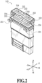
- FIG. 2 is a perspective diagram showing one of the head portions in the liquid ejection head 103 according to the present embodiment, which is explained in FIG. 1 .
- the head portion of the liquid ejection head 103 comprises a liquid ejection unit 202 including a mechanism configured to eject liquid and a common support member 203 configured to supply a plurality of the liquid ejection units 202.
- the head portion of the liquid ejection head 103 comprises a reference member 201 having a function of determining the position with respect to the liquid ejection apparatus 100. By this reference member 201 engaging with an engagement portion (not shown schematically) of the liquid ejection apparatus 100, the position of the liquid ejection head 103 is determined with respect to the liquid ejection apparatus 100.
- the four liquid ejection units 202 are arranged in a staggered pattern on the common support member 203.
- each of the liquid ejection units 202 about 1,000 ejection ports 204 are formed and it is possible for the liquid ejection unit 202 to perform printing with 1,200 dpi by ejecting liquid from the ejection port 204.
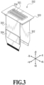
- FIG. 3 is a perspective diagram showing a detailed configuration of the liquid ejection unit 202 shown in FIG. 2 .
- the liquid ejection unit 202 comprises the element substrate 301 including ejection ports ejecting liquid, liquid channels communicating with the ejection ports, energy generation elements and the like, and an electrical wiring substrate 302 electrically connected to the element substrate 301.
- the electrical wiring substrate 302 there are FPC (Flexible Printed Circuits), TAB (Tape Automated Bonding) and the like.
- the liquid ejection unit 202 comprises a support member 303 for reinforcing the element substrate 301.
- the support member 303 is bonded to the ejection surface side of the element substrate 301.
- the electrical wiring substrate 302 is provided with a drive circuit substrate 304 for driving an energy generation element (not shown schematically) generating energy for ejecting liquid.
- an energy generation element a piezoelectric element is used as the energy generation element.
- FIG. 4 is an exploded perspective diagram of the liquid ejection unit 202 in the present embodiment.
- a plurality of electrode terminals 401 is provided along the longitudinal direction.
- an electrical connection section 402 is provided along the transverse direction.
- a conductor for example, wiring line including copper and nickel
- the electrical connection section 402 coming into contact with the electrode terminal 401 the element substrate 301 and the electrical wiring substrate 302 are connected electrically.
- FIG. 5 is a diagram for explaining the configuration for connection between the element substrate 301 and the electrical wiring substrate 302 in the present embodiment.
- first alignment marks 501 are provided, which serve as a reference of registration in a case where the electrical wiring substrate 302 is connected.
- second alignment marks 502 are provided, which serve as a reference of registration with the element substrate 301.
- the element substrate 301 of the present embodiment includes a piezoelectric element as an energy generation element for ejecting liquid.
- the element substrate 301 ejecting liquid by the piezoelectric method is provided with a comparatively large number of electrode terminals 401. Because of this, in the present embodiment, the interval between two adjacent electrode terminals is comparatively narrow. In the situation such as this, in order to connect the electrical connection section 402 to the electrode terminal 401 accurately, it is preferable to perform highly accurate registration by aligning the first alignment marks 501 and the second alignment marks 502 with each other.
- FIG. 6 is a cross-sectional diagram schematically showing the liquid ejection unit 202 in the present embodiment and mainly showing a positional relationship between the electrical connection section 402 of the electrical wiring substrate 302 and the electrode terminal 401 of the element substrate.
- the element substrate 301 comprises a channel forming substrate 601 having a channel (not shown schematically), an actuator substrate 602 having a surface on which the electrode terminal 401 is provided, and an ejection port forming substrate 603 in which the ejection port 204 is formed.
- the actuator substrate 602 is laminated and on the actuator substrate 602, the channel forming substrate 601 is laminated.
- the electrical wiring substrate 302 comprises a base portion 604 including polyimide, a wiring portion 605 including copper and nickel, and a cover portion 606 including solder resist.
- the connection between the element substrate 301 and the electrical wiring substrate 302 is maintained by a non-conductive paste 607.
- a sealing member 608 is applied onto the non-conductive paste 607. It is preferable for the sealing member 608 to have rigidity for protecting the connection between the element substrate 301 and the electrical wiring substrate 302 from an exterior force and to be capable of suppressing corrosion resulting from liquid for ejection, humidity in the environment, and the like.
- the sealing member 608 there is an epoxy resin or the like.
- the example of the sealing member 608 is not limited to the epoxy resin. It is possible to include various materials in accordance with the required performance in the sealing member 608.
- the electrical connection section 402 of the electrical wiring substrate 302 has a connection range 402a connecting with the electrode terminal 401 and a non-connection range 402b adjacent to the connection range 402a and not opposite to the electrode terminal 401.
- the connection range 402a is opposite to the range in which the electrode terminals 401 on the actuator substrate 602 of the element substrate 301 are arrayed and connected to these electrode terminals 401.
- the non-connection range 402b of the electrical connection section 402 has an inclined portion 609 configured to incline in the direction (in the upward direction in FIG. 6 ) in which the inclined portion 609 becomes distant from the actuator substrate 602.
- This inclined portion 609 is formed by the inclination being formed in a manufacturing process to be described in FIG. 8 , FIG. 9A, and FIG. 9B .
- the angle of the inclined portion 609 is 160 degrees or more with respect to a horizontal portion 610 of the electrical connection section 402 substantially parallel to the surface on which the electrode terminal 401 is provided.
- the electrical wiring substrate 302 has an elastic restoring force and the elastic restoring force becomes great as the angle of the inclined portion 609 becomes small. That is, the reason is that it becomes difficult to form and maintain the inclined portion 609 by the above-described inclination formation in a case where the angle of the inclined portion 609 is too small.
- the electrical connection section 402 is configured so that the distance between the highest point of the inclination of the non-connection range 402b and the actuator substrate 602 is greater than the distance between the connection range 402a and the actuator substrate 602.
- the wiring portion 605 being connected to the electrode terminal 401, it is made possible to supply energy and an electric signal for ejecting liquid from the electrical wiring substrate 302 to the element substrate 301. Then, it is made possible for the element substrate 301 to energize the outside by receiving current flowing from the outside, communicate with the outside by receiving an electric signal sent from the outside, and eject liquid via the electrical wiring substrate 302.
- the actuator substrate 602 of the element substrate 301 comprises an energy generation element (piezoelectric element not shown schematically) including an upper electrode film (not shown schematically), a piezoelectric layer (not shown schematically), and a lower electrode film (not shown schematically).
- the actuator substrate 602 changes the volume of the piezoelectric element and ejects liquid droplets from the ejection port 204.
- the channels are divided individually into the number corresponding to the number of ejection ports 204 ejecting liquid droplets and to each individual channel, a piezoelectric element generating a pressure for ejection is attached.
- a piezoelectric element generating a pressure for ejection is attached.
- the number of necessary electrode terminals 401 also increases. In a case where the number of electrode terminals 401 increases, the number of electrodes increases accordingly.
- the non-connection range 402b adjacent to the connection range 402a of the electrical connection section 402 of the electrical wiring substrate 302 inclines with respect to the actuator substrate 602 of the element substrate 301 so that the non-connection range 402b becomes distant from the actuator substrate 602. Consequently, the non-connection range 402b is in the state of being distant from the actuator substrate 602 by the inclined portion 609 formed in advance even in a case where the electrical wiring substrate 302 inclines unintentionally while the wiring portion 605 is being put close to the actuator substrate 602. According to the connection method such as this, in the process of connecting the electrical wiring substrate 302 to the element substrate 301, it is possible to suppress the wiring portion 605 from coming into contact with the actuator substrate 602.
- FIG. 7 is a diagram explaining a positional relationship in the connection between the element substrate 301 and the electrical wiring substrate 302 explained in FIG. 6 .
- FIG. 7 shows a connection process in the liquid ejection head manufacturing process and in this stage, the non-conductive paste 607 and the sealing member 608 (see FIG. 6 ) shown in FIG. 6 are not formed.
- a second distance between the end portion of the element substrate 301 and the electrical wiring substrate 302 is greater than a first distance between the surface on which the electrode terminal 401 is provided and the portion opposite to the electrode terminal 401.
- a distance 702 from the edge of the surface to the non-connection range 402b is greater than a distance 701 from the surface to the connection range 402a.
- connection range 402a of the electrical wiring substrate 302 linear and inclining the non-connection range 402b, it is possible to suppress an unintentional contact between the wiring portion 605 and the actuator substrate 602 described above or the like while appropriately securing the electrical connection.
- liquid ejection unit 202 of the present embodiment which is manufactured by the manufacturing method such as this, to suppress trouble (for example, current leakage, short circuit and the like) that occurs by the wiring portion 605 coming into contact with the actuator substrate 602.
- FIG. 8 is a flowchart showing a manufacturing process of the liquid ejection apparatus 100 in the present embodiment.
- a symbol "S" in the explanation of each process means a step (process) in the flowchart.
- the element substrate 301 (not shown schematically in FIG. 8 ) is set. After this process is completed, the process at S802 is performed.
- the non-conductive paste 607 (not shown schematically in FIG. 8 ) is applied to the electrode terminal 401 (not shown schematically in FIG. 8 ) of the element substrate 301 and around the electrode terminal 401. After this process is completed, the process at S803 is performed.
- hydrophilic treatment for the surface opposite to the element substrate 301 on the electrical wiring substrate 302 (not shown schematically in FIG. 8 ) before the time in point at which the electrical wiring substrate 302 is connected to the element substrate 301.
- hydrophilic treatment for the surface opposite to the element substrate 301 on the electrical wiring substrate 302 (not shown schematically in FIG. 8 ) before the time in point at which the electrical wiring substrate 302 is connected to the element substrate 301.
- wettability improves and the non-conductive paste 607 becomes more likely to spread because of the improvement of wettability, and therefore, it is possible to suppress the non-conductive paste 607 from dropping and flowing into the ejection port 204 (not shown schematically in FIG. 8 ).
- treatment other than hydrophilic treatment for the purpose of suppressing the non-conductive paste 607 from dropping.
- the present disclosure is not limited to performing hydrophilic treatment for the electrical wiring substrate 302.
- the electrical wiring substrate 302 is put close to the element substrate 301. Specifically, the electrical wiring substrate 302 is put close to the surface on which the electrode terminal 401 of the element substrate 301 is provided with the state where the electrical wiring substrate 302 is substantially parallel to the surface being kept by the inclination forming tool 900. After this process is completed, the process at S805 is performed.
- the electrical wiring substrate 302 is connected to the element substrate 301. Specifically, in the state where the connection range 402a of the electrical wiring substrate 302 is in contact with the electrode terminal 401 of the element substrate 301, by using the inclination forming tool 900 (see FIG. 9B ), the connection range 402a is thermally compressed to the electrode terminal 401 from above the base portion 604. After this process is completed, the process at S806 is performed.
- the non-conductive paste 607 is cured. Specifically, in accordance with the curing properties of the non-conductive paste 607 being in use, temperature and time are allowed for the non-conductive paste 607. Then, a force of shrinkage on curing appears and the non-conductive paste 607 cures. By the non-conductive paste 607 curing, the connection between the element substrate 301 and the electrical wiring substrate 302 is maintained. After this process is completed, the process at S807 is performed.
- the sealing member 608 is applied onto the non-conductive paste 607. Through this process, the liquid ejection unit 202 is completed. After this process is completed, the process at S808 is performed.
- the liquid ejection unit 202 is attached to the main body of the liquid ejection head 103 (not shown schematically in FIG. 8 ). Through this process, the liquid ejection head 103 is completed. After this process is completed, the process at S809 is performed.
- the liquid ejection head 103 is attached to a predetermined position of the liquid ejection apparatus 100 (not shown in FIG. 8 ). Through this process, the liquid ejection apparatus 100 is completed.
- FIG. 9A is an explanatory diagram of a process of putting the electrical wiring substrate 302 close to the element substrate 301.
- the electrical wiring substrate 302 is held by the inclination forming tool 900.
- the inclination forming tool 900 has a pressure surface 901 capable of pressing and heating the electrical wiring substrate 302 and an adsorption surface 902 capable of adsorbing and holding the electrical wiring substrate 302.
- the adsorption surface 902 is provided with a suction unit 903 configured to suck in the electrical wiring substrate 302.
- the adsorption surface 902 is located above the pressure surface 901 in the vertical direction.
- FIG. 9B is an explanatory diagram of a process of connecting the electrical wiring substrate 302 to the element substrate 301.
- the non-conductive paste 607 is applied around the electrode terminal 401 on the actuator substrate 602.
- the non-conductive paste 607 cures and the shape of the inclined portion 609 is maintained. That is, also after the point in time at which the inclination forming tool 900 is removed from the electrical wiring substrate 302, by the non-conductive paste 607 having cured, the electrical wiring substrate 302 is supported and the shape of the inclined portion 609 is maintained.
- the temperature and time necessary for curing the non-conductive paste 607 depend on the material included in the non-conductive paste 607.
- FIG. 10A is a diagram showing a state where the electrical wiring substrate 302 is connected correctly to the element substrate 301 in the comparative example.
- a bonding tool 1000 for connecting the electrical wiring substrate 302 to the element substrate 301 is used.
- the bonding tool 1000 was also used in the prior art. It is possible for the bonding tool 1000 to thermally compress the electrical connection section 402 of the electrical wiring substrate 302 to the electrode terminal 401 of the element substrate 301 and the bonding tool 1000 comprises a suction unit 1001 configured to such in the electrical wiring substrate 302. There is no difference in height on the bottom face of the bonding tool 1000 and the inclined portion 609 (see FIG. 6 and FIG. 7 ) is not formed even in a case where the electrical wiring substrate 302 is sucked in by the suction unit 1001.
- FIG. 10B is a diagram showing a state where the electrical wiring substrate 302 is not connected correctly to the element substrate 301 in the comparative example.
- the inclined portion 609 is not formed. Because of this, for example, in a case where the electrical wiring substrate 302 inclines in a state where the bonding tool 1000 holds the electrical wiring substrate 302, there is a possibility that the electrical connection section 402 comes into contact with the actuator substrate 602. That is, in this comparative example, there is a possibility that the above-described trouble occurs.
- the inclined portion 609 (see FIG. 6 and FIG. 7 ) is formed and a large clearance from the actuator substrate 602 to the wiring portion 605 is secured. Consequently, according to the technique of the present disclosure, for example, in a case where the electrical wiring substrate 302 inclines unintentionally in the process of connecting the electrical wiring substrate 302 to the element substrate 301, the electrical connection section 402 is suppressed from coming into contact with the actuator substrate 602.
- liquid ejection head 103 of the present embodiment it is possible to improve the reliability of the connection section between the element substrate 301 and the electrical wiring substrate 302.
- the clearance between the element substrate and the electrical wiring substrate is made large.
- differences from the above-described embodiment are explained mainly. To the same components as those of the above-described embodiment, the same reference symbols are attached and duplicated explanation of those components is omitted appropriately.
- FIG. 11A is a schematic cross-sectional diagram showing the way a process of connecting the electrical wiring substrate 302 to the element substrate 301 is in the present embodiment.
- a concave portion 1101 concave in the direction of becoming distant from the actuator substrate 602 is formed in a state where the electrical wiring substrate 302 is connected to the element substrate 301.
- the concave portion 1101 is located above the edge of the actuator substrate 602 in the vertical direction.
- the concave portion 1101 is formed, it is possible to make large the clearance between the element substrate 301 and the electrical wiring substrate 302 without the need to form an inclined portion. Because of this, it is possible to use the bonding tool 1000 that has been used in the prior art. According to the connection method such as this, it is not necessary to take into consideration the relationship between the elastic restoring force of the electrical wiring substrate 302 and the suction force of the suction unit 1001.
- connection range 402a to the electrode terminal 401 more easily than in the first embodiment.
- FIG. 11B is a schematic cross-sectional diagram for explaining the concave portion 1101 in the present embodiment.
- a deepest portion 402c of the concave portion 1101 is located above the edge of the actuator substrate 602 in the vertical direction.
- the distance from the edge of the actuator substrate 602 to the deepest portion 402c of the concave portion 1101 is greater than the distance from the surface on which the electrode terminal 401 of the actuator substrate 602 is provided to the undersurface of the connection range 402a.
- FIG. 11C is a schematic cross-sectional diagram of a second liquid ejection unit 1100 in the present embodiment.
- the non-conductive paste 607 flowing into the concave portion 1101 the element substrate 301 and the electrical wiring substrate 302 are connected more firmly than in the first embodiment.
- the hydrophilic treatment it is preferable for the hydrophilic treatment to be performed also for the concave portion 1101. The reason is that the non-conductive paste 607 becomes more likely to flow into the concave portion 1101 compared to the case where the hydrophilic treatment is not performed.
- the second liquid ejection unit 1100 it is possible to improve reliability of the connection section between the element substrate 301 and the electrical wiring substrate 302. Further, it is also possible to connect the electrical wiring substrate 302 to the element substrate 301 more easily than in the first embodiment.
- the clearance between the element substrate and the electrical wiring substrate is made large.
- differences from the above described embodiments are explained mainly. To the same components as those of the above-described embodiments, the same reference symbols are attached and duplicated explanation of those components is omitted appropriately.
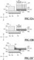
- FIG. 12A is a schematic cross-sectional diagram showing the way a process of connecting the electrical connection section 402 to the electrode terminal 401 is in the present embodiment.
- a step 1201 is formed, which goes down in the direction in which the step 1201 becomes more distant from the electrical connection section 402.
- the step 1201 is located below the non-connection range 402b in the vertical direction.
- FIG. 12B is a schematic cross-sectional diagram for explaining the step 1201 in the present embodiment.
- the distance from the bottom portion of the step 1201 to the undersurface of the non-connection range 402b is greater than the distance from the surface on which the electrode terminal 401 on the actuator substrate 602 is provided to the undersurface of the connection range 402a. According to the configuration such as this, it is possible to make the actuator substrate 602 more distant from the electrical connection section 402 by an amount corresponding to the difference in height in the step 1201.
- FIG. 12C is a schematic cross-sectional diagram of a third liquid ejection unit 1200 in the present embodiment.
- the non-conductive paste 607 staying on the step 1201 the element substrate 301 and the electrical wiring substrate 302 are connected more firmly than in the first embodiment.
- the above-described hydrophilic treatment is performed for the wiring portion 605, it is possible to suppress the non-conductive paste 607 from dropping from the step 1201 compared to the case where the hydrophilic treatment is not performed.
- the third liquid ejection unit 1200 it is possible to improve reliability of the connection section of the element substrate 301 and the electrical wiring substrate 302. Further, it is also possible to connect the electrical wiring substrate 302 to the element substrate 301 more easily than in the first embodiment.
- the manufacturing process of a liquid ejection apparatus is explained, but the order in which each process is performed is not limited as long as it is possible to manufacture a liquid ejection apparatus.
- the order of each process in the manufacturing process of a liquid ejection apparatus may be changed appropriately or the processes may be performed at the same time.
- the liquid is ink
- the liquid to which the technique of the present disclosure can be applied is not limited to ink. That is, as the liquid, various printing liquids including a processing liquid and the like may be used, which are used for the purpose of improving the fixing property of ink in a printing medium, reducing gloss unevenness, and improving scratch resistance.
- the printing medium is a cut sheet
- the printing medium is not limited to a cut sheet as long as it is possible to append liquid to the printing medium.
- the printing medium there are continuous roll paper, plastic, film, fabric, metal, flexible substrate and the like.
- the electrode terminals are provided along both sides of the element substrate, but the electrode terminals may be provided along all the sides of the element substrate.
- the electrical wiring substrate is pulled out of all the end portions on the element substrate. Consequently, compared to the above-described embodiments, it is possible increase the number of electrodes and increase the density of a plurality of formed ejection ports. By increasing the density of the ejection ports, it is made possible to maintain high printing quality also at the time of high-speed printing.
- the energy generation unit is the piezoelectric element
- the example of the energy generation unit is not limited to the piezoelectric element as long as it is possible to append energy necessary for ejection to liquid.
- the energy generation element there is an electrothermal converter.
- the so-called page-wide type liquid ejection head is used, but it is also possible to apply the technique of the present disclosure to a liquid ejection head performing printing while scanning. That is, it is also possible to apply the technique of the present disclosure to the so-called serial type liquid ejection head.
- a plurality of liquid ejection units is arranged on one support member, but it is also possible to appropriately use the technique of the present disclosure for a liquid ejection head in which one liquid ejection unit is arranged on one support member.
- the non-conductive paste is applied to the element substrate, but it may also be possible to connect an electrical wiring element to which the non-conductive paste is applied to an element substrate to which the non-conductive paste is not applied. That is, it is possible to appropriately select which of the element substrate and the electrical wiring substrate the non-conductive paste is applied to in accordance with the configuration of the liquid ejection apparatus.
- the element substrate and the electrical wiring substrate are connected by the non-conductive paste, but the element substrate and the electrical wiring substrate may be connected by an anisotropic conductive film (ACF). Further, it is also possible to connect the element substrate and the electrical wiring substrate by a method, such as a metallic bonding method in which ultrasonic waves, heat and the like are used by using a metal bump formed on an electrode.
- ACF anisotropic conductive film
- the electrical wiring substrate is put close to the element substrate in substantially the parallel (horizontal) state, where the distance between the element substrate and the electrical wiring substrate is made great.
- this manufacturing method it is possible to suppress the contact between the element substrate and the electrical wiring substrate as in the above-described embodiments. Then, for example, it may also be possible to perform subsequent processes after returning the electrical wiring substrate to the normal state and connecting the electrode terminal of the element substrate and the electrical wiring substrate by causing a pressing force to act.
- liquid ejection head of the present disclosure it is possible to improve reliability of the connection section between an element substrate and an electrical wiring substrate.
Landscapes
- Engineering & Computer Science (AREA)
- Manufacturing & Machinery (AREA)
- Particle Formation And Scattering Control In Inkjet Printers (AREA)
Abstract
An object is to provide a liquid ejection head (103) capable of improving reliability of the connection section (402) between an element substrate (301) and an electrical wiring substrate (302). The liquid ejection head (103) ejecting liquid includes an element substrate (301) having a terminal (401) and a wiring substrate (302) including a wiring portion (605) connected to the terminal (401) in contact therewith. In a direction perpendicular to a surface on which the terminal (401) is provided on the element substrate (301), a second distance (702) between the end portion of the element substrate (301) and the wiring portion (605) is greater than a first distance (701) between the surface on which the terminal (401) is provided and a portion opposite to the terminal (401) of the wiring portion (605).
Description
- The present disclosure relates to a liquid ejection head, a liquid ejection apparatus, and a manufacturing method of a liquid ejection head, and in detail, relates to a technique to connect a terminal on a substrate and a wiring portion of a wiring substrate.
- As this type of technique,
Japanese Patent Laid-Open No. 2021-54066 - The process of connecting the wiring portion to the terminal of the substrate is performed in the state where the terminal and the wiring portion are opposite to each other. Because of this, for example, in a case where the wiring substrate inclines unintentionally, it may happen sometimes that the area other than the area opposite to the terminal of the wiring portion comes into contact with the element substrate. As a result of that, there is a possibility that trouble is caused, such as an electrical connection failure.
- An object of the present disclosure is to provide a liquid ejection head capable of improving reliability of the connection section between an element substrate and an electrical wiring substrate.
- The present invention in its first aspect provides a liquid ejection head as specified in claims 1 to 8.
- The present invention in its second aspect provides a liquid ejection apparatus as specified in claim 9.
- The present invention in its third aspect provides a manufacturing method as specified in claims 10 to 14.
- Further features of the present disclosure will become apparent from the following description of exemplary embodiments with reference to the attached drawings.
-
-
FIG. 1 is a diagram showing a configuration of a liquid ejection apparatus according to one embodiment; -
FIG. 2 is a perspective diagram showing one of head portions according to one embodiment; -
FIG. 3 is a perspective diagram showing a configuration of a liquid ejection unit according to one embodiment; -
FIG. 4 is an exploded perspective diagram of a liquid ejection unit according to one embodiment; -
FIG. 5 is a diagram for explaining a configuration for connection according to one embodiment; -
FIG. 6 is a cross-sectional diagram schematically showing a liquid ejection unit according to one embodiment; -
FIG. 7 is a diagram explaining a positional relationship between an element substrate and an electrical wiring substrate according to one embodiment; -
FIG. 8 is a flowchart showing a manufacturing process of a liquid ejection apparatus according to one embodiment; -
FIG. 9A is an explanatory diagram of a process of putting an electrical wiring substrate close to anelement substrate 301; -
FIG. 9B is an explanatory diagram of a process of connecting an electrical wiring substrate to theelement substrate 301; -
FIG. 10A is a diagram showing a state where an electrical wiring substrate is connected to an element substrate correctly in a comparative example; -
FIG. 10B is a diagram showing a state where an electrical wiring substrate is not connected to an element substrate correctly in a comparative example; -
FIG. 11A is a schematic cross-sectional diagram showing the way a process of connecting an electrical wiring substrate to an element substrate is in the present embodiment; -
FIG. 11B is a schematic cross-sectional diagram for explaining a concave portion in the present embodiment; -
FIG. 11C is a schematic cross-sectional diagram of a second liquid ejection unit in the present embodiment; -
FIG. 12A is a schematic cross-sectional diagram showing the way a process of connecting an electrical connection section to an electrical terminal is in the present embodiment; -
FIG. 12B is a schematic cross-sectional diagram for explaining a step in the present embodiment; and -
FIG. 12C is a schematic cross-sectional diagram of a third liquid ejection unit in the present embodiment. -
FIG. 1 is a diagram showing the configuration of aliquid ejection apparatus 100 according to one embodiment of the present disclosure. - First, the coordinate system shown in the drawings referred to in the present specification is explained. As shown in in
FIG 1 , the -Y-direction is the direction in which aprinting medium 101 is conveyed and the -Y-direction is toward the upstream side in the conveyance direction. The X-direction is the longitudinal direction (width direction) of aliquid ejection head 103 and in this case, the transverse direction (depth direction) of theliquid ejection head 103 is the direction along the Y-direction. The Z-direction is the height direction of theliquid ejection head 103. - As shown in
FIG. 1 , theliquid ejection apparatus 100 comprises aconveyance unit 102 configured to convey theprinting medium 101 in the conveyance direction and theliquid ejection head 103 ejecting liquid to theprinting medium 101. - In the present embodiment, a cut sheet is used as the
printing medium 101. Theconveyance unit 102 has a conveyance belt, a conveyance roller pivotally moving the conveyance belt, and the like. In detail, theconveyance unit 102 performs conveyance by adsorbing and holding theprinting medium 101 to the conveyance belt by a suction mechanism, not shown schematically, and pivotally moving the conveyance belt. Theprinting medium 101 for which printing has been performed by the liquid ejection head is peeled off from the conveyance belt by a mechanism, not shown schematically, on the downstream side and discharged to a paper discharge unit (not shown schematically). Theliquid ejection head 103 is the so-called page-wide type liquid ejection head in which ejection ports are arrayed in accordance with the width (length in the X-direction) of theprinting medium 101. - The
liquid ejection head 103 includesliquid ejection heads liquid ejection head 103C ejecting cyan ink is configured by bonding a head portion 103Ca and a head portion 103Cb. Like theliquid ejection head 103C, theliquid ejection head 103M of magenta ink is configured by bonding a head portion 103Ma and a head portion 103Mb. Like theliquid ejection head 103M, theliquid ejection head 103Y of yellow ink is configured by bonding a head portion 103Ya and a head portion 103Yb. Like theliquid ejection head 103Y, theliquid ejection head 103K of black ink is configured by bonding a head portion 103Ka and a head portion 103Kb. In the following, in a case where it is not necessary to particularly distinguish the head portions 103Ca, 103Cb, 103Ma, 103Mb, 103Ya, 103Yb, 103Ka, and 103Kb from one another, they are simply called the head portion. - Each of the
liquid ejection heads liquid ejection heads liquid ejection heads liquid ejection head 103. In the present embodiment, it is possible for theliquid ejection head 103 to perform full-color printing for theprinting medium 101 that is conveyed by ejecting inks of cyan, magenta, yellow, and black. -
FIG. 2 is a perspective diagram showing one of the head portions in theliquid ejection head 103 according to the present embodiment, which is explained inFIG. 1 . - As shown in
FIG. 2 , the head portion of theliquid ejection head 103 comprises aliquid ejection unit 202 including a mechanism configured to eject liquid and acommon support member 203 configured to supply a plurality of theliquid ejection units 202. Further, the head portion of theliquid ejection head 103 comprises areference member 201 having a function of determining the position with respect to theliquid ejection apparatus 100. By thisreference member 201 engaging with an engagement portion (not shown schematically) of theliquid ejection apparatus 100, the position of theliquid ejection head 103 is determined with respect to theliquid ejection apparatus 100. - In the present embodiment, the four
liquid ejection units 202 are arranged in a staggered pattern on thecommon support member 203. In each of theliquid ejection units 202, about 1,000ejection ports 204 are formed and it is possible for theliquid ejection unit 202 to perform printing with 1,200 dpi by ejecting liquid from theejection port 204. -
FIG. 3 is a perspective diagram showing a detailed configuration of theliquid ejection unit 202 shown inFIG. 2 . - As shown in
FIG. 3 , theliquid ejection unit 202 comprises theelement substrate 301 including ejection ports ejecting liquid, liquid channels communicating with the ejection ports, energy generation elements and the like, and anelectrical wiring substrate 302 electrically connected to theelement substrate 301. As one example of theelectrical wiring substrate 302, there are FPC (Flexible Printed Circuits), TAB (Tape Automated Bonding) and the like. - The
liquid ejection unit 202 comprises asupport member 303 for reinforcing theelement substrate 301. Thesupport member 303 is bonded to the ejection surface side of theelement substrate 301. Theelectrical wiring substrate 302 is provided with adrive circuit substrate 304 for driving an energy generation element (not shown schematically) generating energy for ejecting liquid. In the present embodiment, as the energy generation element, a piezoelectric element is used. -
FIG. 4 is an exploded perspective diagram of theliquid ejection unit 202 in the present embodiment. - As shown in
FIG. 4 , at both end portions of theelement substrate 301, a plurality ofelectrode terminals 401 is provided along the longitudinal direction. At the end portion of theelectrical wiring substrate 302, anelectrical connection section 402 is provided along the transverse direction. In theelectrical connection section 402, a conductor (for example, wiring line including copper and nickel) is exposed in the shape of a pad and functions as a connection area with theelectrode terminal 401. By theelectrical connection section 402 coming into contact with theelectrode terminal 401, theelement substrate 301 and theelectrical wiring substrate 302 are connected electrically. -
FIG. 5 is a diagram for explaining the configuration for connection between theelement substrate 301 and theelectrical wiring substrate 302 in the present embodiment. - As shown in
FIG. 5 , at both end portions of theelement substrate 301, first alignment marks 501 are provided, which serve as a reference of registration in a case where theelectrical wiring substrate 302 is connected. On the other hand, at the end portion of theelectrical wiring substrate 302, second alignment marks 502 are provided, which serve as a reference of registration with theelement substrate 301. By this registration, it is possible to perform registration of theelectrical connection section 402 of theelectrical wiring substrate 302 with theelement substrate 301 with accuracy. - As described above, the
element substrate 301 of the present embodiment includes a piezoelectric element as an energy generation element for ejecting liquid. There is a tendency for theelement substrate 301 ejecting liquid by the piezoelectric method to be provided with a comparatively large number ofelectrode terminals 401. Because of this, in the present embodiment, the interval between two adjacent electrode terminals is comparatively narrow. In the situation such as this, in order to connect theelectrical connection section 402 to theelectrode terminal 401 accurately, it is preferable to perform highly accurate registration by aligning the first alignment marks 501 and the second alignment marks 502 with each other. -
FIG. 6 is a cross-sectional diagram schematically showing theliquid ejection unit 202 in the present embodiment and mainly showing a positional relationship between theelectrical connection section 402 of theelectrical wiring substrate 302 and theelectrode terminal 401 of the element substrate. - As shown in
FIG. 6 , theelement substrate 301 comprises achannel forming substrate 601 having a channel (not shown schematically), anactuator substrate 602 having a surface on which theelectrode terminal 401 is provided, and an ejectionport forming substrate 603 in which theejection port 204 is formed. On the ejectionport forming substrate 603, theactuator substrate 602 is laminated and on theactuator substrate 602, thechannel forming substrate 601 is laminated. - The
electrical wiring substrate 302 comprises abase portion 604 including polyimide, awiring portion 605 including copper and nickel, and acover portion 606 including solder resist. The connection between theelement substrate 301 and theelectrical wiring substrate 302 is maintained by anon-conductive paste 607. - Onto the
non-conductive paste 607, a sealingmember 608 is applied. It is preferable for the sealingmember 608 to have rigidity for protecting the connection between theelement substrate 301 and theelectrical wiring substrate 302 from an exterior force and to be capable of suppressing corrosion resulting from liquid for ejection, humidity in the environment, and the like. As one preferable example of the sealingmember 608, there is an epoxy resin or the like. However, the example of the sealingmember 608 is not limited to the epoxy resin. It is possible to include various materials in accordance with the required performance in the sealingmember 608. - As shown in
FIG. 6 , theelectrical connection section 402 of theelectrical wiring substrate 302 has aconnection range 402a connecting with theelectrode terminal 401 and anon-connection range 402b adjacent to theconnection range 402a and not opposite to theelectrode terminal 401. Specifically, theconnection range 402a is opposite to the range in which theelectrode terminals 401 on theactuator substrate 602 of theelement substrate 301 are arrayed and connected to theseelectrode terminals 401. - In the present embodiment, the
non-connection range 402b of theelectrical connection section 402 has aninclined portion 609 configured to incline in the direction (in the upward direction inFIG. 6 ) in which theinclined portion 609 becomes distant from theactuator substrate 602. Thisinclined portion 609 is formed by the inclination being formed in a manufacturing process to be described inFIG. 8 ,FIG. 9A, and FIG. 9B . - It is preferable for the angle of the
inclined portion 609 to be 160 degrees or more with respect to ahorizontal portion 610 of theelectrical connection section 402 substantially parallel to the surface on which theelectrode terminal 401 is provided. The reason is that theelectrical wiring substrate 302 has an elastic restoring force and the elastic restoring force becomes great as the angle of theinclined portion 609 becomes small. That is, the reason is that it becomes difficult to form and maintain theinclined portion 609 by the above-described inclination formation in a case where the angle of theinclined portion 609 is too small. - Further, as details will be described later in
FIG. 7 , theelectrical connection section 402 is configured so that the distance between the highest point of the inclination of thenon-connection range 402b and theactuator substrate 602 is greater than the distance between theconnection range 402a and theactuator substrate 602. - By the
wiring portion 605 being connected to theelectrode terminal 401, it is made possible to supply energy and an electric signal for ejecting liquid from theelectrical wiring substrate 302 to theelement substrate 301. Then, it is made possible for theelement substrate 301 to energize the outside by receiving current flowing from the outside, communicate with the outside by receiving an electric signal sent from the outside, and eject liquid via theelectrical wiring substrate 302. - In the present embodiment, the
actuator substrate 602 of theelement substrate 301 comprises an energy generation element (piezoelectric element not shown schematically) including an upper electrode film (not shown schematically), a piezoelectric layer (not shown schematically), and a lower electrode film (not shown schematically). In a case of receiving a signal supplied from thewiring portion 605 via theelectrode terminal 401, theactuator substrate 602 changes the volume of the piezoelectric element and ejects liquid droplets from theejection port 204. - On the
element substrate 301 adopting the piezoelectric method, the channels are divided individually into the number corresponding to the number ofejection ports 204 ejecting liquid droplets and to each individual channel, a piezoelectric element generating a pressure for ejection is attached. In a case where an attempt is made to form theejection ports 204 in a high density without changing the dimensions and the like of theelement substrate 301, it becomes necessary to increase the number of piezoelectric elements. Accompanying an increase in the number of piezoelectric elements, the number ofnecessary electrode terminals 401 also increases. In a case where the number ofelectrode terminals 401 increases, the number of electrodes increases accordingly. - As explained above, according to the connection configuration of the present embodiment, the
non-connection range 402b adjacent to theconnection range 402a of theelectrical connection section 402 of theelectrical wiring substrate 302 inclines with respect to theactuator substrate 602 of theelement substrate 301 so that thenon-connection range 402b becomes distant from theactuator substrate 602. Consequently, thenon-connection range 402b is in the state of being distant from theactuator substrate 602 by theinclined portion 609 formed in advance even in a case where theelectrical wiring substrate 302 inclines unintentionally while thewiring portion 605 is being put close to theactuator substrate 602. According to the connection method such as this, in the process of connecting theelectrical wiring substrate 302 to theelement substrate 301, it is possible to suppress thewiring portion 605 from coming into contact with theactuator substrate 602. -
FIG. 7 is a diagram explaining a positional relationship in the connection between theelement substrate 301 and theelectrical wiring substrate 302 explained inFIG. 6 . -
FIG. 7 shows a connection process in the liquid ejection head manufacturing process and in this stage, thenon-conductive paste 607 and the sealing member 608 (seeFIG. 6 ) shown inFIG. 6 are not formed. - As shown in
FIG. 7 , in the direction perpendicular to the surface on which theelectrode terminal 401 is provided, a second distance between the end portion of theelement substrate 301 and theelectrical wiring substrate 302 is greater than a first distance between the surface on which theelectrode terminal 401 is provided and the portion opposite to theelectrode terminal 401. - Specifically, in the direction perpendicular to the surface on which the
electrode terminal 401 is provided on theactuator substrate 602, adistance 702 from the edge of the surface to thenon-connection range 402b is greater than adistance 701 from the surface to theconnection range 402a. - Due to this, in the process of connecting the
electrical wiring substrate 302 to theelement substrate 301, for example, even in a case where theelectrical wiring substrate 302 inclines unintentionally, it is possible to suppress the situation in which thewiring portion 605 comes into contact with theactuator substrate 602 and so on, which will be caused by the inclination. - Further, by keeping the
connection range 402a of theelectrical wiring substrate 302 linear and inclining thenon-connection range 402b, it is possible to suppress an unintentional contact between thewiring portion 605 and theactuator substrate 602 described above or the like while appropriately securing the electrical connection. - It is possible for the
liquid ejection unit 202 of the present embodiment, which is manufactured by the manufacturing method such as this, to suppress trouble (for example, current leakage, short circuit and the like) that occurs by thewiring portion 605 coming into contact with theactuator substrate 602. -
FIG. 8 is a flowchart showing a manufacturing process of theliquid ejection apparatus 100 in the present embodiment. A symbol "S" in the explanation of each process means a step (process) in the flowchart. - At S801, the element substrate 301 (not shown schematically in
FIG. 8 ) is set. After this process is completed, the process at S802 is performed. - At S802, the non-conductive paste 607 (not shown schematically in
FIG. 8 ) is applied to the electrode terminal 401 (not shown schematically inFIG. 8 ) of theelement substrate 301 and around theelectrode terminal 401. After this process is completed, the process at S803 is performed. - Further, it may also be possible to perform hydrophilic treatment for the surface opposite to the
element substrate 301 on the electrical wiring substrate 302 (not shown schematically inFIG. 8 ) before the time in point at which theelectrical wiring substrate 302 is connected to theelement substrate 301. On the surface for which the hydrophilic treatment has been performed, wettability improves and thenon-conductive paste 607 becomes more likely to spread because of the improvement of wettability, and therefore, it is possible to suppress thenon-conductive paste 607 from dropping and flowing into the ejection port 204 (not shown schematically inFIG. 8 ). It may also be possible to perform treatment other than hydrophilic treatment for the purpose of suppressing thenon-conductive paste 607 from dropping. Further, the present disclosure is not limited to performing hydrophilic treatment for theelectrical wiring substrate 302. - At S803, registration between the
element substrate 301 and theelectrical wiring substrate 302 is performed. Before the point in time at which this process is performed, theelectrical wiring substrate 302 is held in the state of being sucked by an inclination forming tool 900 (seeFIG. 9A ), to be described later. After this process is completed, the process at S804 is performed. - At S804, the
electrical wiring substrate 302 is put close to theelement substrate 301. Specifically, theelectrical wiring substrate 302 is put close to the surface on which theelectrode terminal 401 of theelement substrate 301 is provided with the state where theelectrical wiring substrate 302 is substantially parallel to the surface being kept by theinclination forming tool 900. After this process is completed, the process at S805 is performed. - At S805, the
electrical wiring substrate 302 is connected to theelement substrate 301. Specifically, in the state where theconnection range 402a of theelectrical wiring substrate 302 is in contact with theelectrode terminal 401 of theelement substrate 301, by using the inclination forming tool 900 (seeFIG. 9B ), theconnection range 402a is thermally compressed to theelectrode terminal 401 from above thebase portion 604. After this process is completed, the process at S806 is performed. - At S806, the
non-conductive paste 607 is cured. Specifically, in accordance with the curing properties of thenon-conductive paste 607 being in use, temperature and time are allowed for thenon-conductive paste 607. Then, a force of shrinkage on curing appears and thenon-conductive paste 607 cures. By thenon-conductive paste 607 curing, the connection between theelement substrate 301 and theelectrical wiring substrate 302 is maintained. After this process is completed, the process at S807 is performed. - At S807, the sealing
member 608 is applied onto thenon-conductive paste 607. Through this process, theliquid ejection unit 202 is completed. After this process is completed, the process at S808 is performed. - At S808, the
liquid ejection unit 202 is attached to the main body of the liquid ejection head 103 (not shown schematically inFIG. 8 ). Through this process, theliquid ejection head 103 is completed. After this process is completed, the process at S809 is performed. - At S809, the
liquid ejection head 103 is attached to a predetermined position of the liquid ejection apparatus 100 (not shown inFIG. 8 ). Through this process, theliquid ejection apparatus 100 is completed. - The above is the explanation of the flowchart of the manufacturing process of the
liquid ejection apparatus 100. -
FIG. 9A is an explanatory diagram of a process of putting theelectrical wiring substrate 302 close to theelement substrate 301. - As shown in
FIG. 9A , before the point in time at which the process of putting theelectrical wiring substrate 302 close to theelement substrate 301 is performed, theelectrical wiring substrate 302 is held by theinclination forming tool 900. Theinclination forming tool 900 has apressure surface 901 capable of pressing and heating theelectrical wiring substrate 302 and anadsorption surface 902 capable of adsorbing and holding theelectrical wiring substrate 302. Theadsorption surface 902 is provided with asuction unit 903 configured to suck in theelectrical wiring substrate 302. Theadsorption surface 902 is located above thepressure surface 901 in the vertical direction. - Consequently, in a case where the
electrical wiring substrate 302 is sucked up by thesuction unit 903 in a state where theelectrical wiring substrate 302 is in contact with thepressure surface 901, part closer to the inside than the portion in contact with thepressure surface 901 comes into close contact with theadsorption surface 902. That is, in a case where theelectrical wiring substrate 302 is sucked up in a state where theelectrical wiring substrate 302 is in contact with thepressure surface 901, theelectrical wiring substrate 302 deforms elastically and theinclined portion 609 is formed. However, in a case where the suction by thesuction unit 903 stops, theelectrical wiring substrate 302 returns to the original shape by the elastic restoring force. -
FIG. 9B is an explanatory diagram of a process of connecting theelectrical wiring substrate 302 to theelement substrate 301. - As shown in
FIG. 9B , before the point in time at which the process of connecting theelectrical wiring substrate 302 to theelement substrate 301, thenon-conductive paste 607 is applied around theelectrode terminal 401 on theactuator substrate 602. In a case where thenon-conductive paste 607 is heated and time elapses in a state where theinclined portion 609 is formed by theinclination forming tool 900, thenon-conductive paste 607 cures and the shape of theinclined portion 609 is maintained. That is, also after the point in time at which theinclination forming tool 900 is removed from theelectrical wiring substrate 302, by thenon-conductive paste 607 having cured, theelectrical wiring substrate 302 is supported and the shape of theinclined portion 609 is maintained. The temperature and time necessary for curing thenon-conductive paste 607 depend on the material included in thenon-conductive paste 607. - In the following, the contact between the
actuator substrate 602 and theelectrical connection section 402 is explained by showing a comparative example. Explanation of the same configuration as that of the present embodiment is omitted appropriately and points different from those of the present embodiment are explained mainly. -
FIG. 10A is a diagram showing a state where theelectrical wiring substrate 302 is connected correctly to theelement substrate 301 in the comparative example. - As shown in
FIG. 10A , in the comparative example, abonding tool 1000 for connecting theelectrical wiring substrate 302 to theelement substrate 301 is used. Thebonding tool 1000 was also used in the prior art. It is possible for thebonding tool 1000 to thermally compress theelectrical connection section 402 of theelectrical wiring substrate 302 to theelectrode terminal 401 of theelement substrate 301 and thebonding tool 1000 comprises asuction unit 1001 configured to such in theelectrical wiring substrate 302. There is no difference in height on the bottom face of thebonding tool 1000 and the inclined portion 609 (seeFIG. 6 andFIG. 7 ) is not formed even in a case where theelectrical wiring substrate 302 is sucked in by thesuction unit 1001. - Whether or not the
inclined portion 609 is present, as long as it is possible to connect theelectrical wiring substrate 302 to theelement substrate 301 parallelly, the above-described trouble does not occur. -
FIG. 10B is a diagram showing a state where theelectrical wiring substrate 302 is not connected correctly to theelement substrate 301 in the comparative example. - As shown in
FIG. 10B , on theelectrical wiring substrate 302 in the comparative example, theinclined portion 609 is not formed. Because of this, for example, in a case where theelectrical wiring substrate 302 inclines in a state where thebonding tool 1000 holds theelectrical wiring substrate 302, there is a possibility that theelectrical connection section 402 comes into contact with theactuator substrate 602. That is, in this comparative example, there is a possibility that the above-described trouble occurs. - In contrast to this, in the present embodiment, on the
electrical wiring substrate 302, the inclined portion 609 (seeFIG. 6 andFIG. 7 ) is formed and a large clearance from theactuator substrate 602 to thewiring portion 605 is secured. Consequently, according to the technique of the present disclosure, for example, in a case where theelectrical wiring substrate 302 inclines unintentionally in the process of connecting theelectrical wiring substrate 302 to theelement substrate 301, theelectrical connection section 402 is suppressed from coming into contact with theactuator substrate 602. - Consequently, according to the
liquid ejection head 103 of the present embodiment, it is possible to improve the reliability of the connection section between theelement substrate 301 and theelectrical wiring substrate 302. - In the present embodiment, by providing a concave portion in the non-correction range, the clearance between the element substrate and the electrical wiring substrate is made large. In the following, differences from the above-described embodiment are explained mainly. To the same components as those of the above-described embodiment, the same reference symbols are attached and duplicated explanation of those components is omitted appropriately.
-
FIG. 11A is a schematic cross-sectional diagram showing the way a process of connecting theelectrical wiring substrate 302 to theelement substrate 301 is in the present embodiment. - As shown in
FIG. 11A , in thenon-connection range 402b of the present embodiment, aconcave portion 1101 concave in the direction of becoming distant from theactuator substrate 602 is formed in a state where theelectrical wiring substrate 302 is connected to theelement substrate 301. In the state where theelectrical wiring substrate 302 is connected to theelement substrate 301, theconcave portion 1101 is located above the edge of theactuator substrate 602 in the vertical direction. - Further, in the present embodiment, because the
concave portion 1101 is formed, it is possible to make large the clearance between theelement substrate 301 and theelectrical wiring substrate 302 without the need to form an inclined portion. Because of this, it is possible to use thebonding tool 1000 that has been used in the prior art. According to the connection method such as this, it is not necessary to take into consideration the relationship between the elastic restoring force of theelectrical wiring substrate 302 and the suction force of thesuction unit 1001. - Consequently, according to the manufacturing method of the present embodiment, it is possible to thermally compress the
connection range 402a to theelectrode terminal 401 more easily than in the first embodiment. -
FIG. 11B is a schematic cross-sectional diagram for explaining theconcave portion 1101 in the present embodiment. - As shown in
FIG. 11B , in the state where theelectrical wiring substrate 302 is connected to theelement substrate 301, adeepest portion 402c of theconcave portion 1101 is located above the edge of theactuator substrate 602 in the vertical direction. - Further, in the
electrical connection section 402 of the present embodiment, in a case where the thickness of theconnection range 402a is taken to be "F" and the thickness from the adhesion surface with thebase portion 604 to thedeepest portion 402c of theconcave portion 1101 is taken to be "F"', formula (1) below holds.
- According to the configuration such as this, the distance from the edge of the
actuator substrate 602 to thedeepest portion 402c of theconcave portion 1101 is greater than the distance from the surface on which theelectrode terminal 401 of theactuator substrate 602 is provided to the undersurface of theconnection range 402a. - Consequently, at the portion at which the
concave portion 1101 is provided in thenon-connection range 402b, it is possible to make thewiring portion 605 distant from theactuator substrate 602 by an amount corresponding to the depth in theconcave portion 1101. That is, it is possible to reduce the possibility that thewiring portion 605 comes into contact with theactuator substrate 602 in the process of connecting theelectrical wiring substrate 302 to theelement substrate 301. -
FIG. 11C is a schematic cross-sectional diagram of a secondliquid ejection unit 1100 in the present embodiment. - As shown in
FIG. 11C , by thenon-conductive paste 607 flowing into theconcave portion 1101, theelement substrate 301 and theelectrical wiring substrate 302 are connected more firmly than in the first embodiment. In a case where the above-described hydrophilic treatment is performed, it is preferable for the hydrophilic treatment to be performed also for theconcave portion 1101. The reason is that thenon-conductive paste 607 becomes more likely to flow into theconcave portion 1101 compared to the case where the hydrophilic treatment is not performed. - Consequently, according to the second
liquid ejection unit 1100, it is possible to improve reliability of the connection section between theelement substrate 301 and theelectrical wiring substrate 302. Further, it is also possible to connect theelectrical wiring substrate 302 to theelement substrate 301 more easily than in the first embodiment. - In the present embodiment, by providing a step at the edge of the actuator substrate, the clearance between the element substrate and the electrical wiring substrate is made large. In the following, differences from the above described embodiments are explained mainly. To the same components as those of the above-described embodiments, the same reference symbols are attached and duplicated explanation of those components is omitted appropriately.
-
FIG. 12A is a schematic cross-sectional diagram showing the way a process of connecting theelectrical connection section 402 to theelectrode terminal 401 is in the present embodiment. - As shown in
FIG. 12A , at the edge of theactuator substrate 602 of the present embodiment, in the state where theelectrical wiring substrate 302 is connected to theelement substrate 301, astep 1201 is formed, which goes down in the direction in which thestep 1201 becomes more distant from theelectrical connection section 402. In the state where theelectrical wiring substrate 302 is connected to theelement substrate 301, thestep 1201 is located below thenon-connection range 402b in the vertical direction. -
FIG. 12B is a schematic cross-sectional diagram for explaining thestep 1201 in the present embodiment. - As shown in
FIG. 12B , in the present embodiment, the distance from the bottom portion of thestep 1201 to the undersurface of thenon-connection range 402b is greater than the distance from the surface on which theelectrode terminal 401 on theactuator substrate 602 is provided to the undersurface of theconnection range 402a. According to the configuration such as this, it is possible to make theactuator substrate 602 more distant from theelectrical connection section 402 by an amount corresponding to the difference in height in thestep 1201. - Consequently, in the process of connecting the
electrical connection section 402 to theelectrode terminal 401, it is possible to reduce the possibility that thewiring portion 605 comes into contact with theactuator substrate 602. -
FIG. 12C is a schematic cross-sectional diagram of a thirdliquid ejection unit 1200 in the present embodiment. - As shown in
FIG. 12C , by thenon-conductive paste 607 staying on thestep 1201, theelement substrate 301 and theelectrical wiring substrate 302 are connected more firmly than in the first embodiment. In a case where the above-described hydrophilic treatment is performed for thewiring portion 605, it is possible to suppress thenon-conductive paste 607 from dropping from thestep 1201 compared to the case where the hydrophilic treatment is not performed. - Consequently, according to the third
liquid ejection unit 1200, it is possible to improve reliability of the connection section of theelement substrate 301 and theelectrical wiring substrate 302. Further, it is also possible to connect theelectrical wiring substrate 302 to theelement substrate 301 more easily than in the first embodiment. - As above, the example to which the technique of the present disclosure can be applied is explained, but the technical scope of the present disclosure is not limited to the above-described example. The first, second, and third embodiments may be combined appropriately.
- In the above-described embodiments, the manufacturing process of a liquid ejection apparatus is explained, but the order in which each process is performed is not limited as long as it is possible to manufacture a liquid ejection apparatus. The order of each process in the manufacturing process of a liquid ejection apparatus may be changed appropriately or the processes may be performed at the same time.
- In the above-described embodiments, explanation is given by supposing the case where the liquid is ink, but the liquid to which the technique of the present disclosure can be applied is not limited to ink. That is, as the liquid, various printing liquids including a processing liquid and the like may be used, which are used for the purpose of improving the fixing property of ink in a printing medium, reducing gloss unevenness, and improving scratch resistance.
- In the above-described embodiments, explanation is given by supposing the case where the printing medium is a cut sheet, but the printing medium is not limited to a cut sheet as long as it is possible to append liquid to the printing medium. As another example of the printing medium, there are continuous roll paper, plastic, film, fabric, metal, flexible substrate and the like.
- In the above-described embodiments, the electrode terminals are provided along both sides of the element substrate, but the electrode terminals may be provided along all the sides of the element substrate. In this case, the electrical wiring substrate is pulled out of all the end portions on the element substrate. Consequently, compared to the above-described embodiments, it is possible increase the number of electrodes and increase the density of a plurality of formed ejection ports. By increasing the density of the ejection ports, it is made possible to maintain high printing quality also at the time of high-speed printing.
- In the above-described embodiments, explanation is given by supposing the case where the energy generation unit is the piezoelectric element, but the example of the energy generation unit is not limited to the piezoelectric element as long as it is possible to append energy necessary for ejection to liquid. As another example of the energy generation element, there is an electrothermal converter. For example, it may also be possible to eject liquid from an election port by causing air bubbles to occur by giving heat to the liquid by using a heater as an electrothermal converter. It is also possible to apply the technique of the present disclosure to the so-called thermal liquid ejection unit such as this.
- In the above-described embodiments, the so-called page-wide type liquid ejection head is used, but it is also possible to apply the technique of the present disclosure to a liquid ejection head performing printing while scanning. That is, it is also possible to apply the technique of the present disclosure to the so-called serial type liquid ejection head.
- In the above-described embodiments, a plurality of liquid ejection units is arranged on one support member, but it is also possible to appropriately use the technique of the present disclosure for a liquid ejection head in which one liquid ejection unit is arranged on one support member.
- In the above-described embodiments, the non-conductive paste is applied to the element substrate, but it may also be possible to connect an electrical wiring element to which the non-conductive paste is applied to an element substrate to which the non-conductive paste is not applied. That is, it is possible to appropriately select which of the element substrate and the electrical wiring substrate the non-conductive paste is applied to in accordance with the configuration of the liquid ejection apparatus.
- In the above-described embodiments, the element substrate and the electrical wiring substrate are connected by the non-conductive paste, but the element substrate and the electrical wiring substrate may be connected by an anisotropic conductive film (ACF). Further, it is also possible to connect the element substrate and the electrical wiring substrate by a method, such as a metallic bonding method in which ultrasonic waves, heat and the like are used by using a metal bump formed on an electrode.
- In the process of connecting the electrical wiring substrate to the element substrate in the first, second, and third embodiments, the electrical wiring substrate is put close to the element substrate in substantially the parallel (horizontal) state, where the distance between the element substrate and the electrical wiring substrate is made great. However, it is also possible to suppress an unintentional contact between the element substrate and the electrical wiring substrate by applying the technique of the present disclosure to the manufacturing method. That is, in a case where the electrical wiring substrate is put close to the element substrate in the connection process, it may also be possible to bring about the state where the more distant the electrical wiring substrate becomes from the electrode terminal by inclining the whole electrical wiring substrate, the greater the distance from the element substrate becomes. According to this manufacturing method, it is possible to suppress the contact between the element substrate and the electrical wiring substrate as in the above-described embodiments. Then, for example, it may also be possible to perform subsequent processes after returning the electrical wiring substrate to the normal state and connecting the electrode terminal of the element substrate and the electrical wiring substrate by causing a pressing force to act.
- In the above-described embodiments, explanation is given by supposing the connection between the electrode terminal and the wiring line. However, the technique of the present disclosure is not limited to the connection between the electrode terminal and the wiring line and it is possible to widely apply the technique of the present disclosure to a technique to connect a terminal
- According to the liquid ejection head of the present disclosure, it is possible to improve reliability of the connection section between an element substrate and an electrical wiring substrate.
- While the present disclosure has been described with reference to exemplary embodiments, it is to be understood that the disclosure is not limited to the disclosed exemplary embodiments. The scope of the following claims is to be accorded the broadest interpretation so as to encompass all such modifications and equivalent structures and functions.
Claims (14)
- A liquid ejection head (103) comprising:an element substrate (301) having a terminal (401); anda wiring substrate (302) including a wiring portion (605) connected to the terminal (401) in contact therewith and bonded to a first surface on which the terminal (401) of the element substrate (301) is provided,characterized in that on the element substrate (301), a plurality of the terminals (401) forms a terminal array arranged along an end portion of the element substrate (301) andin a direction perpendicular to the first surface on the element substrate (301), a second distance (702) between the end portion of the element substrate (301) and the wiring portion (605) is greater than a first distance (701) between the first surface and a portion opposite to the terminal (401) of the wiring portion (605).
- The liquid ejection head (103) according to claim 1, whereinthe wiring substrate (302) has an inclined portion (609) inclining in a direction in which the inclined portion (609) becomes distant from the first surface on the element substrate (301) andin a case of being viewed from a direction perpendicular to the first surface, the inclined portion (609) overlaps the end portion of the element substrate (301).
- The liquid ejection head (103) according to claim 2, wherein
the angle of the inclined portion (609) is 160 degrees or more with respect to the first surface. - The liquid ejection head (103) according to any one of claims 1 to 3, wherein
the wiring portion (605) has a concave portion (1101) concave in a direction in which the concave portion (1101) becomes distant from the first surface on the element substrate (301). - The liquid ejection head (103) according to any one of claims 1 to 4, wherein
the element substrate (301) has a step (1201) more distant from the wiring portion (605) than the first surface. - The liquid ejection head (103) according to any one of claims 1 to 5, further comprising:a non-conductive paste (607) applied between the element substrate (301) and the wiring portion (605), whereinconnection between the wiring portion (605) and the terminal (401) is maintained by the non-conductive paste (607).
- The liquid ejection head (103) according to any one of claims 1 to 6, wherein
the element substrate (301) has an ejection port (204) ejecting liquid and an element generating energy for ejecting liquid from the ejection port (204). - The liquid ejection head (103) according to claim 7, wherein
the element is a piezoelectric element. - A liquid ejection apparatus comprising:
a liquid ejection head (103) according to any one of claims 1 to 7. - A manufacturing method of a liquid ejection head (103) comprising an element substrate (301) having a terminal (401) and a wiring substrate (302) including a wiring portion (605) connected to the terminal (401) in contact therewith and bonded to a first surface on which the terminal (401) of the element substrate (301) is provided, the manufacturing method comprising the step ofconnecting the terminal (401) and the wiring portion (605),characterized in that in the connecting, the terminal (401) is connected to the wiring portion (605) in a state where in a direction perpendicular to the first surface on the element substrate (301), a second distance (702) between the end portion of the element substrate (301) and the wiring portion (605) is greater than a first distance (701) between the first surface and a portion opposite to the terminal (401) of the wiring portion (605).
- The manufacturing method of a liquid ejection head (103) according to claim 10, comprising the step of
applying a non-conductive paste (607) maintaining connection between the terminal (401) and the wiring portion (605) before the connecting. - The manufacturing method of a liquid ejection head (103) according to claim 10 or 11, wherein
in the connecting, the terminal (401) and the wiring portion (605) are bonded by pressure bonding by a tool (900) for holding the wiring substrate (302). - The manufacturing method of a liquid ejection head (103) according to claim 12, whereinthe tool (900) has a pressure surface pressing the wiring substrate (302) and an adsorption surface located above the pressure surface in the vertical direction and adsorbing the wiring substrate (302) andin the connecting, by part of the wiring substrate (302) being pressed by the pressure surface and by a portion of the wiring substrate (302), which is not pressed by the pressure surface, being sucked up by the adsorption surface, an inclined portion (609) inclining so as to become distant from the terminal (401) is formed on the wiring substrate (302).
- The manufacturing method of a liquid ejection head (103) according to claim 13, comprising the step ofapplying a non-conductive paste (607) maintaining connection between the terminal (401) and the wiring portion (605) before the connecting, whereinin the connecting, the non-conductive paste (607) is cured and the shape of the inclined portion (609) is maintained.
Applications Claiming Priority (1)
| Application Number | Priority Date | Filing Date | Title |
|---|---|---|---|
| JP2023182414A JP2025071964A (en) | 2023-10-24 | 2023-10-24 | Liquid ejection head, liquid ejection device, and method for manufacturing liquid ejection head |
Publications (1)
| Publication Number | Publication Date |
|---|---|
| EP4545305A1 true EP4545305A1 (en) | 2025-04-30 |
Family
ID=93257913
Family Applications (1)
| Application Number | Title | Priority Date | Filing Date |
|---|---|---|---|
| EP24207956.4A Pending EP4545305A1 (en) | 2023-10-24 | 2024-10-22 | Liquid ejection head, liquid ejection apparatus, and manufacturing method of liquid ejection head |
Country Status (3)
| Country | Link |
|---|---|
| US (1) | US20250128513A1 (en) |
| EP (1) | EP4545305A1 (en) |
| JP (1) | JP2025071964A (en) |
Citations (6)
| Publication number | Priority date | Publication date | Assignee | Title |
|---|---|---|---|---|
| US20030193545A1 (en) * | 2002-04-12 | 2003-10-16 | Boucher William R. | Electronic devices having an inorganic film |
| JP2010023491A (en) * | 2008-06-16 | 2010-02-04 | Canon Inc | Liquid ejection recording head |
| JP2011031604A (en) * | 2009-08-04 | 2011-02-17 | Samsung Electro-Mechanics Co Ltd | Ink jet head, manufacturing method of ink jet head, electric connecting device for ink jet head |
| JP5355644B2 (en) * | 2011-08-31 | 2013-11-27 | キヤノン株式会社 | Ink jet print head and method of manufacturing the same |
| JP2021054066A (en) | 2019-09-25 | 2021-04-08 | キヤノン株式会社 | Liquid discharge head and manufacturing method thereof |
| JP2023055114A (en) * | 2021-10-05 | 2023-04-17 | キヤノン株式会社 | Liquid ejection head and manufacturing method therefor |
-
2023
- 2023-10-24 JP JP2023182414A patent/JP2025071964A/en active Pending
-
2024
- 2024-10-22 EP EP24207956.4A patent/EP4545305A1/en active Pending
- 2024-10-23 US US18/923,972 patent/US20250128513A1/en active Pending
Patent Citations (6)
| Publication number | Priority date | Publication date | Assignee | Title |
|---|---|---|---|---|
| US20030193545A1 (en) * | 2002-04-12 | 2003-10-16 | Boucher William R. | Electronic devices having an inorganic film |
| JP2010023491A (en) * | 2008-06-16 | 2010-02-04 | Canon Inc | Liquid ejection recording head |
| JP2011031604A (en) * | 2009-08-04 | 2011-02-17 | Samsung Electro-Mechanics Co Ltd | Ink jet head, manufacturing method of ink jet head, electric connecting device for ink jet head |
| JP5355644B2 (en) * | 2011-08-31 | 2013-11-27 | キヤノン株式会社 | Ink jet print head and method of manufacturing the same |
| JP2021054066A (en) | 2019-09-25 | 2021-04-08 | キヤノン株式会社 | Liquid discharge head and manufacturing method thereof |
| JP2023055114A (en) * | 2021-10-05 | 2023-04-17 | キヤノン株式会社 | Liquid ejection head and manufacturing method therefor |
Also Published As
| Publication number | Publication date |
|---|---|
| US20250128513A1 (en) | 2025-04-24 |
| JP2025071964A (en) | 2025-05-09 |
Similar Documents
| Publication | Publication Date | Title |
|---|---|---|
| US6474790B2 (en) | Ink jet recording head | |
| US7390079B2 (en) | Device mounting structure, device mounting method, electronic apparatus, liquid droplet ejection head, and liquid droplet ejection apparatus | |
| CN107107612B (en) | Liquid ejection head and recording device | |
| US9884483B2 (en) | Liquid jetting apparatus | |
| US7025441B2 (en) | Ink jet print head | |
| US11135838B2 (en) | Liquid ejection head and method of manufacturing same | |
| JP6769034B2 (en) | MEMS devices, liquid injection heads, and liquid injection devices | |
| US20250128513A1 (en) | Liquid ejection head, liquid ejection apparatus, and manufacturing method of liquid ejection head | |
| JP3679740B2 (en) | Ink jet recording head and ink jet recording apparatus | |
| JP2002331667A (en) | Printhead, method of manufacturing printhead, and inkjet printing apparatus | |
| JP2003080713A (en) | Liquid ejection head, head cartridge, and method of manufacturing liquid ejection head | |
| US20150352842A1 (en) | Liquid jet head and liquid jet apparatus | |
| JP2012069548A (en) | Structure and method for connecting wiring board | |
| JP4311721B2 (en) | Recording head and ink jet recording apparatus | |
| JP4117512B2 (en) | Inkjet recording device | |
| JP4080152B2 (en) | Inkjet head manufacturing method, inkjet head, and inkjet recording apparatus | |
| JP6375973B2 (en) | Liquid ejection device and method of manufacturing liquid ejection device | |
| JP5464291B2 (en) | Wiring board connection structure and connection method | |
| JP4145481B2 (en) | Inkjet head manufacturing method, inkjet head, inkjet recording apparatus, and image forming apparatus | |
| US11964486B2 (en) | Liquid ejection head | |
| US8944558B2 (en) | Liquid ejection head and liquid ejection apparatus | |
| JP4420585B2 (en) | Inkjet recording head and inkjet recording apparatus | |
| JP4619103B2 (en) | Recording device | |
| JP2017130477A (en) | Mounting device | |
| JP2007160541A (en) | Inkjet recording head and inkjet recording apparatus |
Legal Events
| Date | Code | Title | Description |
|---|---|---|---|
| PUAI | Public reference made under article 153(3) epc to a published international application that has entered the european phase |
Free format text: ORIGINAL CODE: 0009012 |
|
| STAA | Information on the status of an ep patent application or granted ep patent |
Free format text: STATUS: THE APPLICATION HAS BEEN PUBLISHED |
|
| AK | Designated contracting states |
Kind code of ref document: A1 Designated state(s): AL AT BE BG CH CY CZ DE DK EE ES FI FR GB GR HR HU IE IS IT LI LT LU LV MC ME MK MT NL NO PL PT RO RS SE SI SK SM TR |
|
| STAA | Information on the status of an ep patent application or granted ep patent |
Free format text: STATUS: REQUEST FOR EXAMINATION WAS MADE |
|
| 17P | Request for examination filed |
Effective date: 20251030 |