EP4542839A1 - Inverting buck-boost converter and power converter comprising inverting buck-boost converter - Google Patents
Inverting buck-boost converter and power converter comprising inverting buck-boost converter Download PDFInfo
- Publication number
- EP4542839A1 EP4542839A1 EP23204891.8A EP23204891A EP4542839A1 EP 4542839 A1 EP4542839 A1 EP 4542839A1 EP 23204891 A EP23204891 A EP 23204891A EP 4542839 A1 EP4542839 A1 EP 4542839A1
- Authority
- EP
- European Patent Office
- Prior art keywords
- terminal
- coupled
- buck
- diode
- boost converter
- Prior art date
- Legal status (The legal status is an assumption and is not a legal conclusion. Google has not performed a legal analysis and makes no representation as to the accuracy of the status listed.)
- Withdrawn
Links
Images


Classifications
-
- H—ELECTRICITY
- H02—GENERATION; CONVERSION OR DISTRIBUTION OF ELECTRIC POWER
- H02M—APPARATUS FOR CONVERSION BETWEEN AC AND AC, BETWEEN AC AND DC, OR BETWEEN DC AND DC, AND FOR USE WITH MAINS OR SIMILAR POWER SUPPLY SYSTEMS; CONVERSION OF DC OR AC INPUT POWER INTO SURGE OUTPUT POWER; CONTROL OR REGULATION THEREOF
- H02M3/00—Conversion of DC power input into DC power output
- H02M3/02—Conversion of DC power input into DC power output without intermediate conversion into AC
- H02M3/04—Conversion of DC power input into DC power output without intermediate conversion into AC by static converters
- H02M3/10—Conversion of DC power input into DC power output without intermediate conversion into AC by static converters using discharge tubes with control electrode or semiconductor devices with control electrode
- H02M3/145—Conversion of DC power input into DC power output without intermediate conversion into AC by static converters using discharge tubes with control electrode or semiconductor devices with control electrode using devices of a triode or transistor type requiring continuous application of a control signal
- H02M3/155—Conversion of DC power input into DC power output without intermediate conversion into AC by static converters using discharge tubes with control electrode or semiconductor devices with control electrode using devices of a triode or transistor type requiring continuous application of a control signal using semiconductor devices only
- H02M3/156—Conversion of DC power input into DC power output without intermediate conversion into AC by static converters using discharge tubes with control electrode or semiconductor devices with control electrode using devices of a triode or transistor type requiring continuous application of a control signal using semiconductor devices only with automatic control of output voltage or current, e.g. switching regulators
- H02M3/158—Conversion of DC power input into DC power output without intermediate conversion into AC by static converters using discharge tubes with control electrode or semiconductor devices with control electrode using devices of a triode or transistor type requiring continuous application of a control signal using semiconductor devices only with automatic control of output voltage or current, e.g. switching regulators including plural semiconductor devices as final control devices for a single load
- H02M3/1582—Buck-boost converters
-
- H—ELECTRICITY
- H02—GENERATION; CONVERSION OR DISTRIBUTION OF ELECTRIC POWER
- H02M—APPARATUS FOR CONVERSION BETWEEN AC AND AC, BETWEEN AC AND DC, OR BETWEEN DC AND DC, AND FOR USE WITH MAINS OR SIMILAR POWER SUPPLY SYSTEMS; CONVERSION OF DC OR AC INPUT POWER INTO SURGE OUTPUT POWER; CONTROL OR REGULATION THEREOF
- H02M3/00—Conversion of DC power input into DC power output
- H02M3/02—Conversion of DC power input into DC power output without intermediate conversion into AC
- H02M3/04—Conversion of DC power input into DC power output without intermediate conversion into AC by static converters
- H02M3/10—Conversion of DC power input into DC power output without intermediate conversion into AC by static converters using discharge tubes with control electrode or semiconductor devices with control electrode
- H02M3/145—Conversion of DC power input into DC power output without intermediate conversion into AC by static converters using discharge tubes with control electrode or semiconductor devices with control electrode using devices of a triode or transistor type requiring continuous application of a control signal
- H02M3/155—Conversion of DC power input into DC power output without intermediate conversion into AC by static converters using discharge tubes with control electrode or semiconductor devices with control electrode using devices of a triode or transistor type requiring continuous application of a control signal using semiconductor devices only
- H02M3/156—Conversion of DC power input into DC power output without intermediate conversion into AC by static converters using discharge tubes with control electrode or semiconductor devices with control electrode using devices of a triode or transistor type requiring continuous application of a control signal using semiconductor devices only with automatic control of output voltage or current, e.g. switching regulators
-
- H—ELECTRICITY
- H02—GENERATION; CONVERSION OR DISTRIBUTION OF ELECTRIC POWER
- H02M—APPARATUS FOR CONVERSION BETWEEN AC AND AC, BETWEEN AC AND DC, OR BETWEEN DC AND DC, AND FOR USE WITH MAINS OR SIMILAR POWER SUPPLY SYSTEMS; CONVERSION OF DC OR AC INPUT POWER INTO SURGE OUTPUT POWER; CONTROL OR REGULATION THEREOF
- H02M1/00—Details of apparatus for conversion
- H02M1/0003—Details of control, feedback or regulation circuits
- H02M1/0006—Arrangements for supplying an adequate voltage to the control circuit of converters
Definitions
- the present application relates to buck-boost converters and to power converters comprising buck-boost converters.
- Power converters are devices which generally convert an input electrical power (voltage, current) to an output electrical power (voltage, current).
- an input voltage which may be supplied by a mains voltage from a power network, by a battery in a vehicle or the like is converted to an output power having a voltage and current suitable for a particular appliance.
- Power converters include switched mode power supplies (SMPS), where an operation of a switch, which is switched on and off according to some switching scheme, for example a pulse width modulation scheme, determines the output voltage and/or current.
- SMPS switched mode power supplies
- Such a switch may be controlled by controller, for example based on some feedback indicative of the actual output voltage and/or current.
- Some power converters provide a galvanic isolation, where for example a transformer serves to couple a primary side receiving the input electrical power to a secondary side outputting the output electrical power.
- One type of such power converters providing a galvanic isolation are flyback converters, where operation of a switch on the primary side controls transfers of power to the secondary side.
- a controller controlling the above switch and/or other parts of the power converter must be supplied with power.
- an auxiliary winding of the transformer is used to provide power.
- the output voltage may range from 5V to 48V.
- a buck-boost converter as defined in claim 1 and a power converter as defined in claim 6 are provided.
- the dependent claims define further embodiments.
- a power converter comprising:
- a first terminal of the capacitor is coupled to the first output terminal and a cathode of the second diode, an anode of the second diode is coupled to the first terminal of the inductor and a second terminal of the capacitor is coupled to the second output terminal and the second terminal of the inductor.
- the transistor comprises a first terminal, a second terminal and a control terminal, wherein the transistor is switchable by applying a control signal between the second terminal and the control terminal, wherein the second terminal of the transistor is coupled to a second terminal of the inductor.
- the power converter comprises a buck-boost converter as described above, wherein the first input terminal of the buck-boost converter is coupled to a first terminal of an auxiliary winding of the transformer, and the second input terminal of the buck-boost converter is coupled to a second terminal of the auxiliary winding.
- MOSFETs usually act as unidirectional switches due to the presence of a body diode. This means that in an off-state, a MOSFETs blocks current from the first terminal (drain terminal) to the second terminal (source terminal), while current may still flow via the body diode in the reverse direction via the body diode if the forward voltage of the body diode is exceeded. In an on-state, current may flow in both directions. While MOSFETs are used as examples below, in other embodiments other types of transistors may be used, like bipolar junction transistors (BJTs) or insulated gate bipolar transistors (IGBTs). Also such transistors may be unidirectional switches due to body diode or freewheeling diodes present.
- BJTs bipolar junction transistors
- IGBTs insulated gate bipolar transistors
- the first and second terminals are the collector and emitter terminals, respectively, and in case of a BJT the control terminal is the base terminal.
- transistors based on other semiconductor materials may be used, for example Gallium Nitride (GaN) based transistors.
- GaN Gallium Nitride
- a freewheeling diode may be explicitly provided, as the forward voltage of a body diode of a GaN transistor may be to high to allow current flow, which may be needed in some applications. In other applications, no explicit freewheeling diode may need to be provided.
- Connections or couplings shown in the drawings or described herein refer to electrical connections or couplings unless noted otherwise. Such connections or couplings may be modified, for example, by adding additional elements or removing elements, as long as the general purpose of the connection or coupling, for example to provide a signal, voltage, current etc., is essentially maintained. This means essentially that the connections or couplings shown in the figures and described herein are to be seen as functional connections which may be modified as long as the function of the connection is maintained.
- the connections or couplings, if no intervening element is shown may be implemented as direct connections (e.g. by a metal wire, lead, corresponding part of a metal layer in a chip etc.).
- Embodiments described herein relate to buck-boost converters and to power converters including such buck-boost converters to provide an internal supply voltage for the power converter.
- a buck-boost converter generally is a type of DC to DC converter (i.e. converting one direct current (DC) input voltage to another DC output voltage), where the converter may be operated such that the output voltage magnitude is greater than, equal to or less than the input voltage magnitude.
- Fig. 1A illustrates a buck-boost converter 10 according to an embodiment.
- the buck-boost converter of Fig. 1A converts an input voltage V IN to an output voltage V OUT .
- the topology of Fig. 1A is a so-called inverted topology, where the polarity of the output voltage is opposite to the polarity of the input voltage.
- the input voltage V IN is received at a first input terminal 16A and a second input terminal 16B.
- the output voltage is output between a first output terminal 17A and a second output terminal 17B, which in Fig. 1A corresponds to first and second terminals of a capacitor 15.
- the buck-boost converter further comprises transistor 11, an inductor 13, a first diode 12 and a second diode 14.
- a drain terminal of transistor 11 is coupled to a cathode of a first diode 12, and a source terminal of transistor 11 is coupled to a second terminal of inductor 13.
- An anode of first diode 12 is coupled to second input terminal 16B.
- a first terminal of inductor 13 is coupled to first input terminal 16A.
- a first terminal of capacitor 15 is, as already mentioned, coupled to a first output terminal 17A and furthermore coupled to a cathode of second diode 14, and the anode of second diode 14 is coupled to the first terminal of inductor 13. Moreover, the second terminal of capacitor 15 is coupled to second output terminal 17B and the source terminal of transistor 11.
- Fig. 1B shows a variation of buck-boost converter 10 of Fig. 1A and differs from Fig. 1A only with respect to the placement of the first diode.
- a first diode 12A is provided instead of first diode 12 coupled between the drain terminal of transistor 12 and second input terminal.
- An anode of first diode 12A is coupled to the first terminal of inductor 13, and a cathode of first diode 12A is coupled to first input terminal 16A.
- the drain terminal of transistor 11 is coupled to second input terminal 16B.
- the buck-boost converter of Fig. 1B corresponds to the one of Fig. 1A , and the operation is the same.
- buck-boost converter of Fig. 1A may be replaced by the buck-boost converter of Fig. 1B and vice versa.
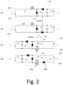
- Fig. 2 Before describing operation of the buck-boost converter of Fig. 1A , referring to Fig. 2 it will be described how the buck-boost converter of Fig. 1A is related to a conventional buck-boost converter, which is shown in line (a) of Fig. 2 .
- the buck-boost converter of Fig. 1A is reproduced in line (d) of Fig. 2 .
- the input voltage V IN is on the left side and the output voltage V OUT is on the right side
- lines (c) und (d) similar to Fig. 1A , the input voltage V IN is on the right side and output voltage V OUT is on the left side.
- the output voltage is provided across capacitor 15, and inductor 13 is provided.
- a transistor 11' is provided between a terminal of inductor 13 and the input voltage.
- the source terminal is coupled to the input terminal, and the drain terminal is coupled to the inductor.
- a cathode of a diode 14' is coupled to the same terminal of inductor 13 as the drain terminal of transistor 11' .
- first diode 14' is "moved" to the position of diode 14, i.e., such that the anode of diode 14 is now coupled to the other terminal of inductor 13 compared to line (a). From line (b) to (c), the representation of the circuit is simply rotated by 180° without changing the circuit. From line (c) to (d), transistor 11' is flipped to result in transistor 11, i.e. the position of the source and drain terminals are exchanged. For isolation, first diode 12 is added.
- a body diode 20 of transistor 11 does not prevent a current flow in a direction from first input terminal 16A via inductor 13 and transistor 11 to second input terminal 16B in an off state of transistor 11.
- first diode 12 or 12B of Fig. 1B
- body diode 20 is explicitly shown only in some of the Figures where it is helpful for explaining the operation, but for example in case of a MOSFET for transistor 11 is a general property of the transistor.
- an isolated gate driver is needed, as the source terminal is coupled to the input voltage.
- transistor 11 may be controlled by a gate driver supplied or based on the output voltage V OUT , which for example in some applications is used as a supply voltage. Therefore, the driver for controlling transistor 11 in line (d) and Fig. 1A can be based on this supply voltage without the need of an isolated driver.
- the operation of the buck-boost converter of Fig. 1A is similar to the operation of the conventional buck-boost converter of line (a) in Fig. 2 .
- the respective transistor (11' or 11) is switched on, the input voltage is connected to the inductor in Fig. 1A with diode 12 allowing current flow only in one direction, effectively decoupling the charging of inductor 13 with energy from capacitor 15.
- capacitor 15 supplies energy to an output load receiving the output voltage V OUT .
- the transistor 11, 11' is switched off, the current in the inductor remains flowing, therefore changing the voltage level over the inductor and allowing to transfer energy from inductor 13 to capacitor 15 via diode 14.
- the magnitude of the output voltage V OUT may be greater than, equal to or smaller than the magnitude of the input voltage V IN .
- a controlling entity (not shown in Fig. 1A ) may measure the output voltage V OUT via any conventional means, for example using a resistive divider, and control transistor 11, 11' accordingly.
- the input voltage V IN may be known e.g. by design, and the duty cycle may be fixed accordingly.
- the regulation may be based on the input voltage V IN with any other signal indicative of the input voltage V IN of the buck-boost converter to regulate the output voltage, as the relation between the input voltage V IN and the output voltage V OUT is, for given inductance values of capacitor 15 and inductor 13, a function of the duty cycle of switch 11, 11'.
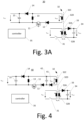
- Fig. 3A illustrates employment of the buck-boost converter of Fig. 1A in a power converter 30 to generate a supply voltage Vvcc .
- the power converter is shown as a schematic flyback converter, converting an input voltage V in2 (not to be confused with the input voltage V IN of Figures 1 and 2 ) to an output voltage V out2 (again not to be confused with the output voltage V OUT of Figures 1 and 2 ).
- the power converter of Fig. 3A comprises a transformer 32 providing a galvanic isolation 32D between a primary side and a secondary side. On a primary side, in the simplified representation of Fig. 3A a switch 31 is coupled to a primary side winding 32A. A secondary side winding 32B is coupled to an output capacitor 34 via a rectifying diode 33. The output voltage is provided across capacitor 34.
- N P :N S is the winding ratio between the primary side winding 32A and the secondary side winding 32B.
- switch 31 By closing switch 31, energy is transferred from the primary side into the transformer (charging), and by opening switch 31, energy is transferred from the transformer to the secondary side (discharging), and the output voltage V out2 is generated in a conventional manner. Operation of switch 31 is controlled by a controller 35.
- the representation of the flyback converter of Fig. 3A is only a schematic example, and any kind of power converter having a transformer for galvanic isolation may be used, and operated in a conventional manner, for example asymmetric half-bridge flyback converters which have a half-bridge arrangement of switches on the primary side.
- asymmetric half-bridge flyback converters which have a half-bridge arrangement of switches on the primary side.
- rectifying diode 33 for example also a synchronous rectifier may be used.
- feedback from the secondary side to the primary side may be used in any conventional manner.
- the flyback converter of Fig. 3A uses a buck-boost converter as discussed with reference to Fig. 1A to provide a supply voltage Vvcc, which supplies for example controller 35. Vvcc therefore corresponds to the output voltage V OUT of Fig. 1A .
- transformer 32 includes an auxiliary winding 32C.
- Auxiliary winding 32C provides a voltage V aux as input voltage to the buck-boost converter.
- a polarity (indicated by dots in Fig. 3A ) of auxiliary winding 32C is selected to be the same as the polarity of primary side winding 32A and opposite the one of secondary side winding 32B, such that the polarity of the voltage Vvcc corresponds to the polarity of V in2 and V out2 in Fig. 3A .
- a usable negative (according to the arrow direction of V aux ) input voltage for the buck-boost converter is provided during the discharge phase of the transformer, and the voltage is proportional to V out2 . If the polarity of auxiliary winding 32 were revised, the input voltage for the buck-boost converter would be proportional to V in2 and usable in the charge phase of the transformer. Both possibilities may be used in embodiments.
- Transistor 11 of the buck-boost converter may also be controlled by controller 35.
- controller 35 need not be a single entity, but may include several entities, for example a first entity for controlling operation of switch 31 and generally the operation of the flyback converter, and a second entity controlling transistor 11.
- entity may be based on different technologies, for example a silicon-based entity and a GaN based entity.
- capacitor 15 may be charged directly from a main supply through a different path (e.g. comprising a resistor and/or depletion cell) until a startup voltage is reached. Then capacitor 15 may provide sufficient energy until V VCC is established. Any conventional startup techniques may be used in this respect.
- controller 35 operates the buck-boost converter only when the polarity of the input voltage V aux to the buck-boost converter is negative, in the configuration of Fig. 3A during the transformer discharge phase of the flyback converter, as then the voltage V aux provided by auxiliary winding 32C has the correct negative polarity to serve as input voltage for the buck-boost converter. This may be achieved by controlling switch 31 and transistor 11 by the same controller, e.g. controller 35. Such a control is further illustrated in Fig. 3B. Fig.
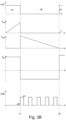
- FIG. 3B schematically shows example signal curves for a control signal ctrl1 controlling switch 31, a primary side current I PRI , a secondary side current I SEC , an auxiliary voltage V aux supplying the buck-boost converter and a control signal ctr12 controlling transistor 11.
- transistor 11 is switched on and off only during the discharge phase between times t1 and t2, where switch 31 is off and V aux is negative.
- the positive value of V aux (before t1 and after t2 in Fig.
- V aux /N P has a magnitude of V in2 (N aux /N P ), where N aux /N P is the winding ratio between auxiliary winding 32C and primary side winding 32A, and the negative value of V aux (between t1 and after t2) has a magnitude of V out2 (N aux /N S ), where N aux /N S is the winding ratio between auxiliary winding 32C and secondary side winding 32B. If the polarity of the auxiliary winding were reversed as explained above, transistor 11 would be operated only in the charge phase, as then V aux again would be negative.
- Fig. 4 shows a power converter 40 according to a further embodiment, where the buck-boost converter may be operated continuously and not only during the transformer discharge phase of the flyback converter.
- the power converter 40 is a variation of the power converter 30 of Fig. 3 , and only differences will explained below.
- the buck-boost converter of Fig. 1A is not directly coupled to auxiliary winding 32C, but a diode 41 and a capacitor 42 are additionally provided as shown.
- Capacitor 42 serves as a buffer provide a continuous input voltage to the buck-boost converter, as the capacitor 42 serves as an energy storage, and diode 41 prevents energy flowing back from capacitor 42 to auxiliary winding 32C and ensures that capacitor 42 is only charged when the voltage provided by auxiliary winding 32C has the "correct" negative polarity for operation of the buck-boost converter, i.e. charging only during the discharge phases of the transformer with the winding polarities shown in Fig. 4 .
- operation of the buck-boost converter need not be limited to the time periods where the voltage V aux is negative, but the buck-boost converter can be operated all the time.
- the buck-boost converter in Fig. 4 can provide a stable voltage V VCC or for example about 12V for a wide range of voltages as auxiliary winding 32, for example in a range from 5V-50V.
- a duty cycle of transistor 11 may be around 7% at 40kHz for a voltage at auxiliary winding of 50V, and for a voltage at the auxiliary winding of 5V the duty cycle may be about 80%.
- Fig. 5 illustrates a power converter 50 according to a further embodiment.
- Power converter 50 is based on power converter 30 of Fig. 3 .
- the power converter of Fig. 1B is used with the diode 12B.
- this is independent from other modifications and may also be done in other embodiments.
- a third diode 51 couples the auxiliary winding, i.e. an input of the buck-boost converter, to a terminal of capacitor 15.
- the buck-boost converter may be used for charging capacitor 15 to generate the output voltage V VCC , especially if V in2 is not high enough to result into sufficient auxiliary winding voltage to charge capacitor 15 via diode 50 directly.
- diode 41 and capacitor 42 may also be provided in power converter 50.
- transistor 11 does not have a body diode allowing charging of capacitor 15 in case of a positive V aux above, e.g. in case of a GaN transistor with high forward voltage of the body diode, an additional freewheeling diode may be provided.
- Fig. 6 shows a variation of the embodiment of Fig. 5 in form of a power converter 60.
- the auxiliary winding is split or has a middle contact between winding parts 32C1 and 32C2.
- the buck-boost converter is coupled to the "full" auxiliary winding (32C1 plus 32C2) to receive a voltage V AUX2 as an input voltage, and a diode 61 corresponding to diode 51 of Fig.
- V AUX1 which directly charges capacitor 15 is coupled to a middle node between winding parts 32C1, 32C2, to receive a voltage V AUX1 . Therefore, the voltage V AUX1 is limited based on a winding ratio of winding parts 32C1, 32C2 and the winding ration N P :N S between primary side winding 32A and secondary side winding 32B.
- the winding ratio N P :N S may be 70:10.
- the winding ratio of part 32C1 to part 32C2 of the auxiliary winding in relation thereto may be 7:3, such that the overall number of turns of the auxiliary winding (32C1 plus 32C2) is equal to the number of turns of secondary side winding 32B.
- a supply voltage of about 15V is available without buck-boost operation.
- the buck-boost converter may take over the provision of V VCC supply.
- the overall auxiliary winding (parts 32C1 to 32C2) has the same number of turns as secondary side winding 32B, which leads to a voltage V AUX2 similar to the output voltage range of V out2 .
- this voltage range V AUX2 may be converted to a supply voltage V VCC of about 15V with a buck or boost operation of the buck-boost converter.
- the above numbers are only examples, and other numbers for the windings and winding ratios may be used.
- secondary side winding and/or auxiliary windings with only one turn may be used.
- auxiliary winding 32C is shown on the primary side of transformer 32, in other embodiments also an auxiliary winding on the secondary side may be used, e.g. to provide a power supply for a secondary side controller.
- Embodiments discussed above may have a lower area requirement and/or lower bill of materials (BOM) compared to conventional solutions.
- a control entity like controller 35 only requires a single terminal to control the buck-boost converter, namely, to control transistor 11.
Landscapes
- Engineering & Computer Science (AREA)
- Power Engineering (AREA)
- Dc-Dc Converters (AREA)
Abstract
Buck-boost converters and corresponding power converters are disclosed. The buck-boost converter includes a transistor (11) having a terminal, e.g. source terminal, coupled to an output terminal (17B) and a terminal of a capacitor (15).
Description
- The present application relates to buck-boost converters and to power converters comprising buck-boost converters.
- Power converters are devices which generally convert an input electrical power (voltage, current) to an output electrical power (voltage, current). For example, an input voltage, which may be supplied by a mains voltage from a power network, by a battery in a vehicle or the like is converted to an output power having a voltage and current suitable for a particular appliance.
- Power converters include switched mode power supplies (SMPS), where an operation of a switch, which is switched on and off according to some switching scheme, for example a pulse width modulation scheme, determines the output voltage and/or current. Such a switch may be controlled by controller, for example based on some feedback indicative of the actual output voltage and/or current.
- Some power converters provide a galvanic isolation, where for example a transformer serves to couple a primary side receiving the input electrical power to a secondary side outputting the output electrical power. One type of such power converters providing a galvanic isolation are flyback converters, where operation of a switch on the primary side controls transfers of power to the secondary side.
- A controller controlling the above switch and/or other parts of the power converter must be supplied with power. In power converters providing a galvanic isolation, sometimes an auxiliary winding of the transformer is used to provide power. As for example in power converters having a variable output voltage also an auxiliary voltage provided by such an auxiliary winding varies, it is desirable to regulate the voltage provided by the auxiliary winding to a predefined value usable by the controller. For example, for a power converter used for USB-PD (Universal Serial Bus - Power Delivery standardized for the USB bus) the output voltage may range from 5V to 48V. With a minimum requirement for example of 12V for supplying a controller, tapped at an auxiliary winding the supply voltage would vary by the same factor as the output voltage, for example from 12V to 115V. Designing a controller operable with his range of supply voltages is difficult, if not impossible.
- Various conventional solutions have been proposed to overcome this issue, for example using a depletion MOSFET together with a Zener diode to clamp the maximum voltage, divided auxiliary windings, combination of clamp circuit and boost converter or a Greinacher half-wave voltage doubler. These solutions, while generally feasible at least in some voltage ranges, may suffer from a high area requirement for implementing the circuit and thus a high bill of materials (BOM) and/or poor power efficiency.
- A buck-boost converter as defined in claim 1 and a power converter as defined in claim 6 are provided. The dependent claims define further embodiments.
- In an embodiment, a power converter is provided comprising:
- a first input terminal and a second input terminal configured to receive an input voltage,
- a first output terminal and a second output terminal configured to provide an output voltage,
- a transistor, an inductor, a capacitor, a first diode and a second diode.
- A first terminal of the capacitor is coupled to the first output terminal and a cathode of the second diode, an anode of the second diode is coupled to the first terminal of the inductor and a second terminal of the capacitor is coupled to the second output terminal and the second terminal of the inductor.
- The transistor comprises a first terminal, a second terminal and a control terminal, wherein the transistor is switchable by applying a control signal between the second terminal and the control terminal,
wherein the second terminal of the transistor is coupled to a second terminal of the inductor. -
- the first diode is provided with an anode coupled to the first terminal of the inductor and a cathode coupled to the first input terminal, and the first terminal of the transistor is coupled to the second input terminal,
or: - a first terminal of the inductor is coupled to the first input terminal
- A primary side configured to receive an input power and being coupled to a primary side winding to a transformer, and a secondary side configured to output an output power and being coupled to a secondary side winding of the transformer. Furthermore, the power converter comprises a buck-boost converter as described above, wherein the first input terminal of the buck-boost converter is coupled to a first terminal of an auxiliary winding of the transformer, and the second input terminal of the buck-boost converter is coupled to a second terminal of the auxiliary winding.
- The above summary is merely a brief overview over some embodiments and is not to be construed as limiting in any way, as other embodiments may include different features.
-
-
Fig. 1A is a circuit diagram of a buck-boost converter according to an embodiment, andFig. 1B shows a variation of the embodiment ofFig. 1A . -
Figure 2 illustrates how the buck-boost converter ofFig. 1 is related to a conventional buck-boost converter. -
Fig. 3A is a circuit diagram of a power converter according to an embodiment. -
Fig. 3B is a timing diagram illustrating operation of the power converter ofFig. 3A . -
Fig. 4 is a circuit diagram of a power converter according to an embodiment. -
Fig. 5 is a circuit diagram of a power converter according to an embodiment. -
Fig. 6 is a circuit diagram of a power converter according to an embodiment. - In the following, various embodiments will be described in detail referring to the attached drawings. These embodiments are given by way of example only and are not to be construed as limiting.
- Features from different embodiments may be combined to form further embodiments. Variations, details, or modifications described with respect to one of the embodiments are also applicable to other embodiments and will therefore not be described repeatedly. In the drawings, like elements are designated with the same reference numerals.
- Embodiments of buck-boost converters described herein use a transistor as a switch. Transistors are described as having a first terminal, a second terminal and a control terminal. Such a transistor is switchable by applying a control signal (voltage or current) between the control terminal and the second terminal. Such transistors may operate as unidirectional switches. In the following embodiments, MOSFETs (metal oxide semiconductor field effect transistors) are used as examples for switch transistors. In this case, the first terminal corresponds to the drain terminal, the second terminal corresponds to the source terminal, and the control terminal corresponds to the gate terminal. Switching is effected by applying a suitable gate-source voltage as control signal. Note that MOSFETs usually act as unidirectional switches due to the presence of a body diode. This means that in an off-state, a MOSFETs blocks current from the first terminal (drain terminal) to the second terminal (source terminal), while current may still flow via the body diode in the reverse direction via the body diode if the forward voltage of the body diode is exceeded. In an on-state, current may flow in both directions. While MOSFETs are used as examples below, in other embodiments other types of transistors may be used, like bipolar junction transistors (BJTs) or insulated gate bipolar transistors (IGBTs). Also such transistors may be unidirectional switches due to body diode or freewheeling diodes present. In case of a BJT or IGBT, the first and second terminals are the collector and emitter terminals, respectively, and in case of a BJT the control terminal is the base terminal. Furthermore, besides silicon based transistors also transistors based on other semiconductor materials may be used, for example Gallium Nitride (GaN) based transistors. In such implementations, a freewheeling diode may be explicitly provided, as the forward voltage of a body diode of a GaN transistor may be to high to allow current flow, which may be needed in some applications. In other applications, no explicit freewheeling diode may need to be provided.
- Connections or couplings shown in the drawings or described herein refer to electrical connections or couplings unless noted otherwise. Such connections or couplings may be modified, for example, by adding additional elements or removing elements, as long as the general purpose of the connection or coupling, for example to provide a signal, voltage, current etc., is essentially maintained. This means essentially that the connections or couplings shown in the figures and described herein are to be seen as functional connections which may be modified as long as the function of the connection is maintained. The connections or couplings, if no intervening element is shown, may be implemented as direct connections (e.g. by a metal wire, lead, corresponding part of a metal layer in a chip etc.).
- Embodiments described herein relate to buck-boost converters and to power converters including such buck-boost converters to provide an internal supply voltage for the power converter. A buck-boost converter generally is a type of DC to DC converter (i.e. converting one direct current (DC) input voltage to another DC output voltage), where the converter may be operated such that the output voltage magnitude is greater than, equal to or less than the input voltage magnitude.
-
Fig. 1A illustrates a buck-boost converter 10 according to an embodiment. The buck-boost converter ofFig. 1A converts an input voltage VIN to an output voltage VOUT. The topology ofFig. 1A is a so-called inverted topology, where the polarity of the output voltage is opposite to the polarity of the input voltage. - The input voltage VIN, as can be seen in
Fig. 1A , is received at afirst input terminal 16A and asecond input terminal 16B. The output voltage is output between afirst output terminal 17A and asecond output terminal 17B, which inFig. 1A corresponds to first and second terminals of acapacitor 15. The buck-boost converter further comprisestransistor 11, aninductor 13, afirst diode 12 and asecond diode 14. - For simplicity's sake, in the following figures the designation of the input and output terminals is omitted and only the input voltage VIN and the output voltage VOUT, or corresponding voltages, are shown.
- A drain terminal of
transistor 11 is coupled to a cathode of afirst diode 12, and a source terminal oftransistor 11 is coupled to a second terminal ofinductor 13. An anode offirst diode 12 is coupled tosecond input terminal 16B. A first terminal ofinductor 13 is coupled tofirst input terminal 16A. - A first terminal of
capacitor 15 is, as already mentioned, coupled to afirst output terminal 17A and furthermore coupled to a cathode ofsecond diode 14, and the anode ofsecond diode 14 is coupled to the first terminal ofinductor 13. Moreover, the second terminal ofcapacitor 15 is coupled tosecond output terminal 17B and the source terminal oftransistor 11. -
Fig. 1B shows a variation of buck-boost converter 10 ofFig. 1A and differs fromFig. 1A only with respect to the placement of the first diode. Instead offirst diode 12 coupled between the drain terminal oftransistor 12 and second input terminal, afirst diode 12A is provided. An anode offirst diode 12A is coupled to the first terminal ofinductor 13, and a cathode offirst diode 12A is coupled tofirst input terminal 16A. Moreover, the drain terminal oftransistor 11 is coupled tosecond input terminal 16B. Otherwise, the buck-boost converter ofFig. 1B corresponds to the one ofFig. 1A , and the operation is the same. In particular,first diode 12B ofFig. 1B serves the same function asfirst diode 12 ofFig. 1A . Therefore, in the embodiments described in the following, the buck-boost converter ofFig. 1A may be replaced by the buck-boost converter ofFig. 1B and vice versa. - Before describing operation of the buck-boost converter of
Fig. 1A , referring toFig. 2 it will be described how the buck-boost converter ofFig. 1A is related to a conventional buck-boost converter, which is shown in line (a) ofFig. 2 . The buck-boost converter ofFig. 1A is reproduced in line (d) ofFig. 2 . Please note that in lines (a) and (b), the input voltage VIN is on the left side and the output voltage VOUT is on the right side, whereas in lines (c) und (d), similar toFig. 1A , the input voltage VIN is on the right side and output voltage VOUT is on the left side. - In the conventional buck-boost converter of line (a) of
Fig. 2 , also the output voltage is provided acrosscapacitor 15, andinductor 13 is provided. A transistor 11' is provided between a terminal ofinductor 13 and the input voltage. Please note that in line (a), the source terminal is coupled to the input terminal, and the drain terminal is coupled to the inductor. A cathode of a diode 14' is coupled to the same terminal ofinductor 13 as the drain terminal of transistor 11' . - To derive the buck-boost converter of
Fig. 1A , first diode 14' is "moved" to the position ofdiode 14, i.e., such that the anode ofdiode 14 is now coupled to the other terminal ofinductor 13 compared to line (a). From line (b) to (c), the representation of the circuit is simply rotated by 180° without changing the circuit. From line (c) to (d), transistor 11' is flipped to result intransistor 11, i.e. the position of the source and drain terminals are exchanged. For isolation,first diode 12 is added. In particular, through the flip, in line (d), in contrast to line (c) abody diode 20 oftransistor 11 does not prevent a current flow in a direction fromfirst input terminal 16A viainductor 13 andtransistor 11 tosecond input terminal 16B in an off state oftransistor 11. Through providing first diode 12 (or 12B ofFig. 1B ), this current flow is still prevented. It should be noted thatbody diode 20 is explicitly shown only in some of the Figures where it is helpful for explaining the operation, but for example in case of a MOSFET fortransistor 11 is a general property of the transistor. - For controlling the conventional boost converter of line (a), an isolated gate driver is needed, as the source terminal is coupled to the input voltage. However, in the buck-boost converter of
Fig. 1A and line (d), as the source terminal is coupled to the output side,transistor 11 may be controlled by a gate driver supplied or based on the output voltage VOUT, which for example in some applications is used as a supply voltage. Therefore, the driver for controllingtransistor 11 in line (d) andFig. 1A can be based on this supply voltage without the need of an isolated driver. - Otherwise, the operation of the buck-boost converter of
Fig. 1A is similar to the operation of the conventional buck-boost converter of line (a) inFig. 2 . When the respective transistor (11' or 11) is switched on, the input voltage is connected to the inductor inFig. 1A withdiode 12 allowing current flow only in one direction, effectively decoupling the charging ofinductor 13 with energy fromcapacitor 15. - In this stage,
capacitor 15 supplies energy to an output load receiving the output voltage VOUT. When thetransistor 11, 11' is switched off, the current in the inductor remains flowing, therefore changing the voltage level over the inductor and allowing to transfer energy frominductor 13 tocapacitor 15 viadiode 14. - Depending on the duty cycle (on-time of
transistor 11, 11' versus off-time oftransistor 11, 11'), the magnitude of the output voltage VOUT may be greater than, equal to or smaller than the magnitude of the input voltage VIN. In some embodiments, a controlling entity (not shown inFig. 1A ) may measure the output voltage VOUT via any conventional means, for example using a resistive divider, andcontrol transistor 11, 11' accordingly. In other embodiments, the input voltage VIN may be known e.g. by design, and the duty cycle may be fixed accordingly. In yet other embodiments, the regulation may be based on the input voltage VIN with any other signal indicative of the input voltage VIN of the buck-boost converter to regulate the output voltage, as the relation between the input voltage VIN and the output voltage VOUT is, for given inductance values ofcapacitor 15 andinductor 13, a function of the duty cycle ofswitch 11, 11'. -
Fig. 3A illustrates employment of the buck-boost converter ofFig. 1A in apower converter 30 to generate a supply voltage Vvcc . - The power converter is shown as a schematic flyback converter, converting an input voltage Vin2 (not to be confused with the input voltage VIN of
Figures 1 and2 ) to an output voltage Vout2 (again not to be confused with the output voltage VOUT ofFigures 1 and2 ). The power converter ofFig. 3A comprises atransformer 32 providing agalvanic isolation 32D between a primary side and a secondary side. On a primary side, in the simplified representation ofFig. 3A aswitch 31 is coupled to a primary side winding 32A. A secondary side winding 32B is coupled to anoutput capacitor 34 via a rectifyingdiode 33. The output voltage is provided acrosscapacitor 34. NP:NS is the winding ratio between the primary side winding 32A and the secondary side winding 32B. - By closing
switch 31, energy is transferred from the primary side into the transformer (charging), and by openingswitch 31, energy is transferred from the transformer to the secondary side (discharging), and the output voltage Vout2 is generated in a conventional manner. Operation ofswitch 31 is controlled by acontroller 35. - The representation of the flyback converter of
Fig. 3A is only a schematic example, and any kind of power converter having a transformer for galvanic isolation may be used, and operated in a conventional manner, for example asymmetric half-bridge flyback converters which have a half-bridge arrangement of switches on the primary side. Instead of rectifyingdiode 33, for example also a synchronous rectifier may be used. Furthermore, feedback from the secondary side to the primary side may be used in any conventional manner. As the design and operation of such converters is known to the skilled person, no further description will be given here. - The flyback converter of
Fig. 3A uses a buck-boost converter as discussed with reference toFig. 1A to provide a supply voltage Vvcc, which supplies forexample controller 35. Vvcc therefore corresponds to the output voltage VOUT ofFig. 1A . - To provide an input voltage to the buck-boost converter,
transformer 32 includes an auxiliary winding 32C. Auxiliary winding 32C provides a voltage Vaux as input voltage to the buck-boost converter. A polarity (indicated by dots inFig. 3A ) of auxiliary winding 32C is selected to be the same as the polarity of primary side winding 32A and opposite the one of secondary side winding 32B, such that the polarity of the voltage Vvcc corresponds to the polarity of Vin2 and Vout2 inFig. 3A . In this case, as will also be explained below, a usable negative (according to the arrow direction of Vaux) input voltage for the buck-boost converter is provided during the discharge phase of the transformer, and the voltage is proportional to Vout2. If the polarity of auxiliary winding 32 were revised, the input voltage for the buck-boost converter would be proportional to Vin2 and usable in the charge phase of the transformer. Both possibilities may be used in embodiments. -
Transistor 11 of the buck-boost converter may also be controlled bycontroller 35. In this respect,controller 35 need not be a single entity, but may include several entities, for example a first entity for controlling operation ofswitch 31 and generally the operation of the flyback converter, and a secondentity controlling transistor 11. Such entity may be based on different technologies, for example a silicon-based entity and a GaN based entity. - As the source terminal of
transistor 11 is coupled to the output side of the buck-boost converter, the control entity and fortransistor 11 need not be isolated, but can be supplied by VVCC. At startup,capacitor 15 may be charged directly from a main supply through a different path (e.g. comprising a resistor and/or depletion cell) until a startup voltage is reached. Thencapacitor 15 may provide sufficient energy until VVCC is established. Any conventional startup techniques may be used in this respect. - In the embodiment of
Fig. 3A ,controller 35 operates the buck-boost converter only when the polarity of the input voltage Vaux to the buck-boost converter is negative, in the configuration ofFig. 3A during the transformer discharge phase of the flyback converter, as then the voltage Vaux provided by auxiliary winding 32C has the correct negative polarity to serve as input voltage for the buck-boost converter. This may be achieved by controllingswitch 31 andtransistor 11 by the same controller,e.g. controller 35. Such a control is further illustrated inFig. 3B. Fig. 3B schematically shows example signal curves for a control signalctrl1 controlling switch 31, a primary side current IPRI, a secondary side current ISEC, an auxiliary voltage Vaux supplying the buck-boost converter and a control signalctr12 controlling transistor 11. As can be seen,transistor 11 is switched on and off only during the discharge phase between times t1 and t2, whereswitch 31 is off and Vaux is negative. For the configuration ofFig. 3A , the positive value of Vaux (before t1 and after t2 inFig. 3B ) has a magnitude of Vin2(Naux/NP), where Naux/NP is the winding ratio between auxiliary winding 32C and primary side winding 32A, and the negative value of Vaux (between t1 and after t2) has a magnitude of Vout2(Naux/NS), where Naux/NS is the winding ratio between auxiliary winding 32C and secondary side winding 32B. If the polarity of the auxiliary winding were reversed as explained above,transistor 11 would be operated only in the charge phase, as then Vaux again would be negative. -
Fig. 4 shows apower converter 40 according to a further embodiment, where the buck-boost converter may be operated continuously and not only during the transformer discharge phase of the flyback converter. Thepower converter 40 is a variation of thepower converter 30 ofFig. 3 , and only differences will explained below. - In
power converters 40, the buck-boost converter ofFig. 1A is not directly coupled to auxiliary winding 32C, but adiode 41 and acapacitor 42 are additionally provided as shown.Capacitor 42 serves as a buffer provide a continuous input voltage to the buck-boost converter, as thecapacitor 42 serves as an energy storage, anddiode 41 prevents energy flowing back fromcapacitor 42 to auxiliary winding 32C and ensures thatcapacitor 42 is only charged when the voltage provided by auxiliary winding 32C has the "correct" negative polarity for operation of the buck-boost converter, i.e. charging only during the discharge phases of the transformer with the winding polarities shown inFig. 4 . - In the embodiment of
Fig. 4 , through the provision ofdiode 41 and capacitor 44, operation of the buck-boost converter need not be limited to the time periods where the voltage Vaux is negative, but the buck-boost converter can be operated all the time. - Simulations have shown that the buck-boost converter in
Fig. 4 can provide a stable voltage VVCC or for example about 12V for a wide range of voltages as auxiliary winding 32, for example in a range from 5V-50V. For example, in such a case, a duty cycle oftransistor 11 may be around 7% at 40kHz for a voltage at auxiliary winding of 50V, and for a voltage at the auxiliary winding of 5V the duty cycle may be about 80%. -
Fig. 5 illustrates apower converter 50 according to a further embodiment.Power converter 50 is based onpower converter 30 ofFig. 3 . Compared toFig. 3 , the power converter ofFig. 1B is used with thediode 12B. As already explained, this is independent from other modifications and may also be done in other embodiments. Moreover, athird diode 51 couples the auxiliary winding, i.e. an input of the buck-boost converter, to a terminal ofcapacitor 15. - In the embodiment of
Fig. 5 , when Vaux is positive (charge phase of the transformer for the polarities shown), if the input voltage Vin2 is highenough capacitor 15 is charged with the positive auxiliary winding voltage VAUX viadiode 51 andbody diode 20 oftransistor 11, for example if Vin2 is of the order of 400V. Note that to enable this charging, in the embodiment ofFig. 5 diode 12B as inFig. 1B is used, asdiode 12 ofFig. 1A would block the charging. In the discharge phase of the transformer, VAUX is negative (corresponding to the different polarities of input and output voltage of the buck-boost converter inFig. 1B ), the buck-boost converter may be used for chargingcapacitor 15 to generate the output voltage VVCC, especially if Vin2 is not high enough to result into sufficient auxiliary winding voltage to chargecapacitor 15 viadiode 50 directly. In other embodiments, additionallydiode 41 andcapacitor 42 may also be provided inpower converter 50. Furthermore, incase transistor 11 does not have a body diode allowing charging ofcapacitor 15 in case of a positive Vaux above, e.g. in case of a GaN transistor with high forward voltage of the body diode, an additional freewheeling diode may be provided. - The charging of
capacitor 15 viadiode 51 may be problematic in some applications with high Vin2, leading to high voltages VAUX provided by auxiliary winding 32C (e.g. VAUX significantly exceeding the required voltage VVCC).Fig. 6 shows a variation of the embodiment ofFig. 5 in form of apower converter 60. Inpower converter 60 ofFig. 6 , the auxiliary winding is split or has a middle contact between winding parts 32C1 and 32C2. The buck-boost converter is coupled to the "full" auxiliary winding (32C1 plus 32C2) to receive a voltage VAUX2 as an input voltage, and adiode 61 corresponding todiode 51 ofFig. 5 , which directly chargescapacitor 15, is coupled to a middle node between winding parts 32C1, 32C2, to receive a voltage VAUX1. Therefore, the voltage VAUX1 is limited based on a winding ratio of winding parts 32C1, 32C2 and the winding ration NP:NS between primary side winding 32A and secondary side winding 32B. - As a numerical example, the winding ratio NP:NS may be 70:10. The winding ratio of part 32C1 to part 32C2 of the auxiliary winding in relation thereto may be 7:3, such that the overall number of turns of the auxiliary winding (32C1 plus 32C2) is equal to the number of turns of secondary side winding 32B.
- In case of an input voltage Vin2 of 400V the voltage VAUX1 at the auxiliary winding part 32C2 with would be 400V x 3/70=17.14V. Subtracting the forward voltage drop-
off diode 61 and thetransistor body diode 20, a supply voltage of about 15V is available without buck-boost operation. If Vin2 is lower, the buck-boost converter may take over the provision of VVCC supply. In this example, the overall auxiliary winding (parts 32C1 to 32C2) has the same number of turns as secondary side winding 32B, which leads to a voltage VAUX2 similar to the output voltage range of Vout2. In case of a full range USB-PD voltage Vout2 from about 5V to about 48V, this means that this voltage range VAUX2 may be converted to a supply voltage VVCC of about 15V with a buck or boost operation of the buck-boost converter. The above numbers are only examples, and other numbers for the windings and winding ratios may be used. For example, in some embodiments secondary side winding and/or auxiliary windings with only one turn may be used. - It should be noted that while in the above embodiments the auxiliary winding 32C is shown on the primary side of
transformer 32, in other embodiments also an auxiliary winding on the secondary side may be used, e.g. to provide a power supply for a secondary side controller. - Embodiments discussed above may have a lower area requirement and/or lower bill of materials (BOM) compared to conventional solutions. Moreover, a control entity like
controller 35 only requires a single terminal to control the buck-boost converter, namely, to controltransistor 11. - Some embodiments are defined by the following examples:
- Example 1. A buck-boost converter, comprising:
- a first input terminal and a second input terminal configured to receive an input voltage,
- a first output terminal and a second output terminal configured to provide an output voltage,
- a transistor, an inductor, a capacitor, a first diode and a second diode,
- wherein a first terminal of the capacitor is coupled to the first output terminal and a cathode of the second diode, an anode of the second diode is coupled to the first terminal of the inductor and a second terminal of the capacitor is coupled to the second output terminal and the second terminal of the inductor wherein the transistor comprises a first terminal, a second terminal and a control terminal,
- wherein the transistor is switchable by applying a control signal between the second terminal and the control terminal,
- wherein the second terminal of the transistor is coupled to a second terminal of the inductor,
- wherein either:
- the first diode is provided with an anode coupled to the first terminal of the inductor and a cathode coupled to the first input terminal, and the first terminal of the transistor is coupled to the second input terminal,
or - a first terminal of the inductor is coupled to the first input terminal
- the first diode is provided with an anode coupled to the first terminal of the inductor and a cathode coupled to the first input terminal, and the first terminal of the transistor is coupled to the second input terminal,
- the first diode is provided with the anode coupled to the second input terminal and the cathode coupled to the first terminal of the transistor.
- Example 2. The buck-boost converter of example 1, further comprising a controller configured to control the transistor such that the buck-boost converter generates the output voltage based on the input voltage.
- Example 3. The buck-boost converter of example 1 or 2, further comprising:
a further capacitor and a third diode, wherein a first terminal of the further capacitor is coupled to the first input terminal, the first terminal of the inductor and the anode of the second diode, a second terminal of the further capacitor is coupled to the drain terminal of the transistor and a cathode of the third diode, and wherein an anode of the third diode is coupled to the second input terminal. - Example 4. The buck-boost converter of any one of examples 1 to 3, further comprising a fourth diode, wherein an anode of the fourth diode is coupled to the first input terminal, and a cathode of the fourth diode is coupled to the first terminal of the capacitor.
- Example 5. The buck-boost converter of any one of examples 1 to 3,
further comprising a fifth diode, wherein an anode of the fifth diode is coupled to a third input terminal, and a cathode of the fifth diode is coupled to the first terminal of the capacitor. - Example 6. The buck-boost converter of any one of examples 1 to 5, wherein the transistor is a MOSFET transistor, the first terminal of the transistor is a drain terminal and the second terminal of the transistor is a source terminal.
- Example 7. A power converter, comprising:
- a primary side configured to receive an input power and
- coupled to a primary side winding of a transformer,
- a secondary side configured to output an output power and coupled to a secondary side winding of the transformer, and the buck-boost converter of any one of examples 1 to 6,
- wherein the first input terminal of the buck-boost converter is coupled to a first terminal of an auxiliary winding of the transformer, and the second input terminal of the buck-boost converter is coupled to a second terminal of the auxiliary winding.
- Example 8. The power converter of example 7, wherein the buck-boost converter is the buck-boost converter of example 5, wherein the third input terminal of the buck-boost converter is coupled to a middle terminal of the auxiliary winding between the first terminal and the second terminal.
- Example 9. The power converter of example 8, wherein the auxiliary winding is on a primary side of the transformer, wherein a ratio of a number of windings between the middle terminal and the second terminal of the auxiliary winding to a number of windings of the primary side winding is selected such that for a predefined nominal input voltage the fifth diode provides a desired output voltage to the capacitor.
- Example 10. The power converter of any one of examples 7 to 9, further comprising a power converter controller coupled to the first and second output terminals of the buck-boost converter to be supplied by the output voltage of the buck-boost converter.
- Although specific embodiments have been illustrated and described herein, it will be appreciated by those of ordinary skill in the art that a variety of alternate and/or equivalent implementations may be substituted for the specific embodiments shown and described without departing from the scope of the present invention. This application is intended to cover any adaptations or variations of the specific embodiments discussed herein. Therefore, it is intended that this invention be limited only by the claims and the equivalents thereof.
Claims (10)
- A buck-boost converter (10), comprising:a first input terminal (16A) and a second input terminal (16B) configured to receive an input voltage (VIN),a first output terminal (17A) and a second output terminal (17B) configured to provide an output voltage (VOUT, VVCC),a transistor (11), an inductor (13), a capacitor (15), a first diode (12, 12B) and a second diode (14),wherein a first terminal of the capacitor (15) is coupled to the first output terminal (17A) and a cathode of the second diode (14), an anode of the second diode (14) is coupled to the first terminal of the inductor (13) and a second terminal of the capacitor (15) is coupled to the second output terminal (17B) and the second terminal of the inductor (13)wherein the transistor (11) comprises a first terminal, a second terminal and a control terminal,wherein the transistor is switchable by applying a control signal between the second terminal and the control terminal,wherein the second terminal of the transistor (11) is coupled to a second terminal of the inductor (13),wherein either:- the first diode (12B) is provided with an anode coupled to the first terminal of the inductor (13) and a cathode coupled to the first input terminal (16A), and the first terminal of the transistor (11) is coupled to the second input terminal (16B),
or- a first terminal of the inductor (13) is coupled to the first input terminal (16A)the first diode (12) is provided with the anode coupled to the second input terminal (16B) and the cathode coupled to the first terminal of the transistor (11). - The buck-boost converter (10) of claim 1, further comprising a controller (35) configured to control the transistor (11) such that the buck-boost converter (10) generates the output voltage (VOUT, VVCC) based on the input voltage (VIN).
- The buck-boost converter (10) of claim 1 or 2, further comprising:
a further capacitor (42) and a third diode (41), wherein a first terminal of the further capacitor (42) is coupled to the first input terminal (16A), the first terminal of the inductor (13) and the anode of the second diode (14), a second terminal of the further capacitor (42) is coupled to the drain terminal of the transistor (11) and a cathode of the third diode (41), and wherein an anode of the third diode (41) is coupled to the second input terminal (16B). - The buck-boost converter (10) of any one of claims 1 to 3, further comprising a fourth diode (51), wherein an anode of the fourth diode (51) is coupled to the first input terminal (16A), and a cathode of the fourth diode (51) is coupled to the first terminal of the capacitor (15).
- The buck-boost converter (10) of any one of claims 1 to 3,
further comprising a fifth diode (61), wherein an anode of the fifth diode (61) is coupled to a third input terminal, and a cathode of the fifth diode (61) is coupled to the first terminal of the capacitor (15). - The buck-boost converter (10) of any one of claims 1 to 5, wherein the transistor (11) is a MOSFET transistor, the first terminal of the transistor (11) is a drain terminal and the second terminal of the transistor (11) is a source terminal.
- A power converter (30, 40, 50, 60), comprising:a primary side configured to receive an input power and coupled to a primary side winding (32A) of a transformer (32),a secondary side configured to output an output power and coupled to a secondary side winding (32B) of the transformer (32), andthe buck-boost converter (10) of any one of claims 1 to 6,wherein the first input terminal (16A) of the buck-boost converter (10) is coupled to a first terminal of an auxiliary winding (32C) of the transformer (32), and the second input terminal (16B) of the buck-boost converter (10) is coupled to a second terminal of the auxiliary winding (32C).
- The power converter (30, 40, 50, 60) of claim 7, wherein the buck-boost converter (10) is the buck-boost converter (10) of claim 5, wherein the third input terminal of the buck-boost converter (10) is coupled to a middle terminal of the auxiliary winding (32C) between the first terminal and the second terminal.
- The power converter of claim 8, wherein the auxiliary winding (32C) is on a primary side of the transformer (32), wherein a ratio of a number of windings between the middle terminal and the second terminal of the auxiliary winding to a number of windings of the primary side winding is selected such that for a predefined nominal input voltage the fifth diode (61) provides a desired output voltage to the capacitor (15) .
- The power converter of any one of claims 7 to 9, further comprising a power converter controller (35) coupled to the first and second output terminals (17A, 17B) of the buck-boost converter (10) to be supplied by the output voltage (VOUT, VVCC) of the buck-boost converter (10) .
Priority Applications (3)
| Application Number | Priority Date | Filing Date | Title |
|---|---|---|---|
| EP23204891.8A EP4542839A1 (en) | 2023-10-20 | 2023-10-20 | Inverting buck-boost converter and power converter comprising inverting buck-boost converter |
| DE102024126417.9A DE102024126417A1 (en) | 2023-10-20 | 2024-09-13 | Power converter that includes a buck-boost converter |
| CN202411453334.4A CN119865061A (en) | 2023-10-20 | 2024-10-17 | Power converter including buck-boost converter |
Applications Claiming Priority (1)
| Application Number | Priority Date | Filing Date | Title |
|---|---|---|---|
| EP23204891.8A EP4542839A1 (en) | 2023-10-20 | 2023-10-20 | Inverting buck-boost converter and power converter comprising inverting buck-boost converter |
Publications (1)
| Publication Number | Publication Date |
|---|---|
| EP4542839A1 true EP4542839A1 (en) | 2025-04-23 |
Family
ID=88506649
Family Applications (1)
| Application Number | Title | Priority Date | Filing Date |
|---|---|---|---|
| EP23204891.8A Withdrawn EP4542839A1 (en) | 2023-10-20 | 2023-10-20 | Inverting buck-boost converter and power converter comprising inverting buck-boost converter |
Country Status (3)
| Country | Link |
|---|---|
| EP (1) | EP4542839A1 (en) |
| CN (1) | CN119865061A (en) |
| DE (1) | DE102024126417A1 (en) |
Citations (3)
| Publication number | Priority date | Publication date | Assignee | Title |
|---|---|---|---|---|
| US20080304293A1 (en) * | 2007-06-05 | 2008-12-11 | O2Micro Inc | Converter controller |
| CN109327158A (en) * | 2018-09-30 | 2019-02-12 | 中南大学 | A current-mode grid-connected inverter device integrating power decoupling and buck-boost functions |
| EP3796531A1 (en) * | 2018-07-09 | 2021-03-24 | Huawei Technologies Co., Ltd. | Control circuit applied to power adapter, and power adapter |
-
2023
- 2023-10-20 EP EP23204891.8A patent/EP4542839A1/en not_active Withdrawn
-
2024
- 2024-09-13 DE DE102024126417.9A patent/DE102024126417A1/en active Pending
- 2024-10-17 CN CN202411453334.4A patent/CN119865061A/en active Pending
Patent Citations (3)
| Publication number | Priority date | Publication date | Assignee | Title |
|---|---|---|---|---|
| US20080304293A1 (en) * | 2007-06-05 | 2008-12-11 | O2Micro Inc | Converter controller |
| EP3796531A1 (en) * | 2018-07-09 | 2021-03-24 | Huawei Technologies Co., Ltd. | Control circuit applied to power adapter, and power adapter |
| CN109327158A (en) * | 2018-09-30 | 2019-02-12 | 中南大学 | A current-mode grid-connected inverter device integrating power decoupling and buck-boost functions |
Non-Patent Citations (2)
| Title |
|---|
| ALONSO J M ET AL: "A NOVEL LOW-COST HIGH-POWER-FACTOR INTEGRATED BALLAST FOR FLUORESCENT LAMPS", IECON '98. PROCEEDINGS OF THE 24TH ANNUAL CONFERENCE OF THE IEEE INDUSTRIAL ELECTRONICS SOCIETY. AACHEN, AUG. 31 - SEPT. 4, 1998; [ANNUAL CONFERENCE OF THE IEEE INDUSTRIAL ELECTRONICS SOCIETY], NEW YORK, NY : IEEE, US, 31 August 1998 (1998-08-31), pages 941 - 946, XP000801203, ISBN: 978-0-7803-4504-1, DOI: 10.1109/IECON.1998.724220 * |
| SIVAKUMAR P ET AL: "Analysis and enhancement of PV efficiency with incremental conductance MPPT technique under non-linear loading conditions", RENEWABLE ENERGY, vol. 81, 9 April 2015 (2015-04-09), pages 543 - 550, XP029157619, ISSN: 0960-1481, DOI: 10.1016/J.RENENE.2015.03.062 * |
Also Published As
| Publication number | Publication date |
|---|---|
| CN119865061A (en) | 2025-04-22 |
| DE102024126417A1 (en) | 2025-04-24 |
Similar Documents
| Publication | Publication Date | Title |
|---|---|---|
| US8488355B2 (en) | Driver for a synchronous rectifier and power converter employing the same | |
| US7924579B2 (en) | Fly-forward converter power supply | |
| US6421262B1 (en) | Active rectifier | |
| US6717388B2 (en) | Bidirectional converter with input voltage control by a primary switch and output voltage regulation by a secondary switch | |
| CN214281239U (en) | Switch mode power converter and inductive charging circuit for same | |
| CN102007677A (en) | Bidirectional dc/dc converter and power conditioner | |
| US10727753B2 (en) | Bidirectional flyback converter circuit | |
| US6317341B1 (en) | Switching circuit, method of operation thereof and single stage power factor corrector employing the same | |
| US20170331385A1 (en) | Dc/dc converter | |
| US6999325B2 (en) | Current/voltage converter arrangement | |
| US20190386574A1 (en) | Power supply and power supply unit | |
| US20020172057A1 (en) | Power supply arrangement comprising a DC/DC converter | |
| US11637489B2 (en) | Isolated DC/DC converter and AC/DC converter | |
| JP4605532B2 (en) | Multi-output type switching power supply | |
| JP6803993B2 (en) | DC voltage converter and how to operate the DC voltage converter | |
| TWI767535B (en) | Method and apparatus for generating control signal and charging dc supply in a secondary synchronous rectifier | |
| US12531488B2 (en) | Asymmetric half bridge flyback converter | |
| JP2001231258A (en) | DC-DC converter | |
| JP4361334B2 (en) | DC / DC converter | |
| CN119865061A (en) | Power converter including buck-boost converter | |
| CN110301088B (en) | Power supply units and power supply units | |
| JP6942040B2 (en) | Insulated switching power supply | |
| JP2002320385A (en) | Switching converter | |
| JP6945429B2 (en) | Insulated switching power supply | |
| CN116707275B (en) | Auxiliary circuit, power supply system and electronic equipment |
Legal Events
| Date | Code | Title | Description |
|---|---|---|---|
| PUAI | Public reference made under article 153(3) epc to a published international application that has entered the european phase |
Free format text: ORIGINAL CODE: 0009012 |
|
| STAA | Information on the status of an ep patent application or granted ep patent |
Free format text: STATUS: THE APPLICATION HAS BEEN PUBLISHED |
|
| AK | Designated contracting states |
Kind code of ref document: A1 Designated state(s): AL AT BE BG CH CY CZ DE DK EE ES FI FR GB GR HR HU IE IS IT LI LT LU LV MC ME MK MT NL NO PL PT RO RS SE SI SK SM TR |
|
| STAA | Information on the status of an ep patent application or granted ep patent |
Free format text: STATUS: THE APPLICATION IS DEEMED TO BE WITHDRAWN |
|
| 18D | Application deemed to be withdrawn |
Effective date: 20251024 |