EP4542656A1 - Semiconductor device - Google Patents
Semiconductor device Download PDFInfo
- Publication number
- EP4542656A1 EP4542656A1 EP23823828.1A EP23823828A EP4542656A1 EP 4542656 A1 EP4542656 A1 EP 4542656A1 EP 23823828 A EP23823828 A EP 23823828A EP 4542656 A1 EP4542656 A1 EP 4542656A1
- Authority
- EP
- European Patent Office
- Prior art keywords
- semiconductor region
- semiconductor
- semiconductor device
- view
- region
- Prior art date
- Legal status (The legal status is an assumption and is not a legal conclusion. Google has not performed a legal analysis and makes no representation as to the accuracy of the status listed.)
- Pending
Links
Images


Classifications
-
- H—ELECTRICITY
- H10—SEMICONDUCTOR DEVICES; ELECTRIC SOLID-STATE DEVICES NOT OTHERWISE PROVIDED FOR
- H10D—INORGANIC ELECTRIC SEMICONDUCTOR DEVICES
- H10D8/00—Diodes
- H10D8/60—Schottky-barrier diodes
-
- H—ELECTRICITY
- H10—SEMICONDUCTOR DEVICES; ELECTRIC SOLID-STATE DEVICES NOT OTHERWISE PROVIDED FOR
- H10D—INORGANIC ELECTRIC SEMICONDUCTOR DEVICES
- H10D62/00—Semiconductor bodies, or regions thereof, of devices having potential barriers
- H10D62/10—Shapes, relative sizes or dispositions of the regions of the semiconductor bodies; Shapes of the semiconductor bodies
- H10D62/102—Constructional design considerations for preventing surface leakage or controlling electric field concentration
- H10D62/103—Constructional design considerations for preventing surface leakage or controlling electric field concentration for increasing or controlling the breakdown voltage of reverse-biased devices
- H10D62/105—Constructional design considerations for preventing surface leakage or controlling electric field concentration for increasing or controlling the breakdown voltage of reverse-biased devices by having particular doping profiles, shapes or arrangements of PN junctions; by having supplementary regions, e.g. junction termination extension [JTE]
- H10D62/106—Constructional design considerations for preventing surface leakage or controlling electric field concentration for increasing or controlling the breakdown voltage of reverse-biased devices by having particular doping profiles, shapes or arrangements of PN junctions; by having supplementary regions, e.g. junction termination extension [JTE] having supplementary regions doped oppositely to or in rectifying contact with regions of the semiconductor bodies, e.g. guard rings with PN or Schottky junctions
-
- H—ELECTRICITY
- H10—SEMICONDUCTOR DEVICES; ELECTRIC SOLID-STATE DEVICES NOT OTHERWISE PROVIDED FOR
- H10D—INORGANIC ELECTRIC SEMICONDUCTOR DEVICES
- H10D62/00—Semiconductor bodies, or regions thereof, of devices having potential barriers
- H10D62/10—Shapes, relative sizes or dispositions of the regions of the semiconductor bodies; Shapes of the semiconductor bodies
- H10D62/102—Constructional design considerations for preventing surface leakage or controlling electric field concentration
- H10D62/103—Constructional design considerations for preventing surface leakage or controlling electric field concentration for increasing or controlling the breakdown voltage of reverse-biased devices
- H10D62/105—Constructional design considerations for preventing surface leakage or controlling electric field concentration for increasing or controlling the breakdown voltage of reverse-biased devices by having particular doping profiles, shapes or arrangements of PN junctions; by having supplementary regions, e.g. junction termination extension [JTE]
- H10D62/106—Constructional design considerations for preventing surface leakage or controlling electric field concentration for increasing or controlling the breakdown voltage of reverse-biased devices by having particular doping profiles, shapes or arrangements of PN junctions; by having supplementary regions, e.g. junction termination extension [JTE] having supplementary regions doped oppositely to or in rectifying contact with regions of the semiconductor bodies, e.g. guard rings with PN or Schottky junctions
- H10D62/107—Buried supplementary regions, e.g. buried guard rings
-
- H—ELECTRICITY
- H10—SEMICONDUCTOR DEVICES; ELECTRIC SOLID-STATE DEVICES NOT OTHERWISE PROVIDED FOR
- H10D—INORGANIC ELECTRIC SEMICONDUCTOR DEVICES
- H10D62/00—Semiconductor bodies, or regions thereof, of devices having potential barriers
- H10D62/10—Shapes, relative sizes or dispositions of the regions of the semiconductor bodies; Shapes of the semiconductor bodies
- H10D62/102—Constructional design considerations for preventing surface leakage or controlling electric field concentration
- H10D62/103—Constructional design considerations for preventing surface leakage or controlling electric field concentration for increasing or controlling the breakdown voltage of reverse-biased devices
- H10D62/105—Constructional design considerations for preventing surface leakage or controlling electric field concentration for increasing or controlling the breakdown voltage of reverse-biased devices by having particular doping profiles, shapes or arrangements of PN junctions; by having supplementary regions, e.g. junction termination extension [JTE]
- H10D62/108—Constructional design considerations for preventing surface leakage or controlling electric field concentration for increasing or controlling the breakdown voltage of reverse-biased devices by having particular doping profiles, shapes or arrangements of PN junctions; by having supplementary regions, e.g. junction termination extension [JTE] having localised breakdown regions, e.g. built-in avalanching regions
-
- H—ELECTRICITY
- H10—SEMICONDUCTOR DEVICES; ELECTRIC SOLID-STATE DEVICES NOT OTHERWISE PROVIDED FOR
- H10D—INORGANIC ELECTRIC SEMICONDUCTOR DEVICES
- H10D62/00—Semiconductor bodies, or regions thereof, of devices having potential barriers
- H10D62/10—Shapes, relative sizes or dispositions of the regions of the semiconductor bodies; Shapes of the semiconductor bodies
- H10D62/102—Constructional design considerations for preventing surface leakage or controlling electric field concentration
- H10D62/112—Constructional design considerations for preventing surface leakage or controlling electric field concentration for preventing surface leakage due to surface inversion layers, e.g. by using channel stoppers
-
- H—ELECTRICITY
- H10—SEMICONDUCTOR DEVICES; ELECTRIC SOLID-STATE DEVICES NOT OTHERWISE PROVIDED FOR
- H10D—INORGANIC ELECTRIC SEMICONDUCTOR DEVICES
- H10D62/00—Semiconductor bodies, or regions thereof, of devices having potential barriers
- H10D62/10—Shapes, relative sizes or dispositions of the regions of the semiconductor bodies; Shapes of the semiconductor bodies
- H10D62/124—Shapes, relative sizes or dispositions of the regions of semiconductor bodies or of junctions between the regions
- H10D62/126—Top-view geometrical layouts of the regions or the junctions
-
- H—ELECTRICITY
- H10—SEMICONDUCTOR DEVICES; ELECTRIC SOLID-STATE DEVICES NOT OTHERWISE PROVIDED FOR
- H10D—INORGANIC ELECTRIC SEMICONDUCTOR DEVICES
- H10D62/00—Semiconductor bodies, or regions thereof, of devices having potential barriers
- H10D62/60—Impurity distributions or concentrations
-
- H—ELECTRICITY
- H10—SEMICONDUCTOR DEVICES; ELECTRIC SOLID-STATE DEVICES NOT OTHERWISE PROVIDED FOR
- H10D—INORGANIC ELECTRIC SEMICONDUCTOR DEVICES
- H10D64/00—Electrodes of devices having potential barriers
- H10D64/111—Field plates
-
- H—ELECTRICITY
- H10—SEMICONDUCTOR DEVICES; ELECTRIC SOLID-STATE DEVICES NOT OTHERWISE PROVIDED FOR
- H10D—INORGANIC ELECTRIC SEMICONDUCTOR DEVICES
- H10D8/00—Diodes
- H10D8/20—Breakdown diodes, e.g. avalanche diodes
- H10D8/25—Zener diodes
-
- H—ELECTRICITY
- H10—SEMICONDUCTOR DEVICES; ELECTRIC SOLID-STATE DEVICES NOT OTHERWISE PROVIDED FOR
- H10D—INORGANIC ELECTRIC SEMICONDUCTOR DEVICES
- H10D84/00—Integrated devices formed in or on semiconductor substrates that comprise only semiconducting layers, e.g. on Si wafers or on GaAs-on-Si wafers
- H10D84/101—Integrated devices comprising main components and built-in components, e.g. IGBT having built-in freewheel diode
Definitions
- the present invention relates to a semiconductor device.
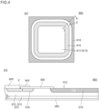
- Fig. 4 is a view for describing a conventional semiconductor device 900.
- Fig. 4(a) is a plan view of the semiconductor device 900
- Fig. 4(b) is a cross-sectional view of the semiconductor device 900 taken along a line A-A in Fig. 4(a).
- Fig.4(b) may be also referred to as a cross-sectional view of a corner portion C of the semiconductor device 900.
- Fig. 4(a) is a plan view of the semiconductor device 900
- Fig. 4(b) is a cross-sectional view of the semiconductor device 900 taken along a line A-A in Fig. 4(a).
- Fig.4(b) may be also referred to as a cross-sectional view of a corner portion C of the semiconductor device 900.
- Fig. 4(a) is a plan view of the semiconductor device 900
- Fig. 4(b) is a cross-sectional view of the semiconductor device 900 taken along
- a first electrode 920, an insulation layer 930 and a field plate 940 disposed on a first main surface of a semiconductor base body 910 are not illustrated.
- the conventional semiconductor device 900 includes: the semiconductor base body 910, the first electrode 920 that is disposed on the first main surface of the semiconductor base body 910, the insulation layer 930 that is disposed on the first main surface so as to surround the first electrode 920 as viewed in a plan view, the field plate 940 that is connected to the first electrode 920 and is disposed on the insulation layer 930, and a second electrode 950 that is disposed on a second main surface of the semiconductor base body 910 on a side opposite to the first main surface.
- the semiconductor base body 910 has a first semiconductor region 912 of an n-type (an n - -type semiconductor region 913 and a n ++ -type semiconductor region 914), and the guard ring 916 of a p-type, and a channel stopper 918 of an n + -type that is spaced apart from the guard ring 916 and is disposed on an outer edge side of the guard ring 916.
- an outer edge of the corner portion C of the guard ring 916 has been formed in an arc shape as viewed in a plan view (see Fig. 4(a) ).
- Patent Literature 1 JP-A-05-75100
- a contact edge E (a portion near a boundary between the first electrode 920 and the insulation layer 920 in the semiconductor base body 910) is liable to be broken when a reverse bias is applied to the semiconductor device thus giving rise to a drawback that it is difficult for the semiconductor device to increase its breakdown strength.
- the present invention has been made so as to overcome the above-mentioned drawback, and it is an object of the present invention to provide a semiconductor device capable of increasing breakdown strength thereof compared to the conventional semiconductor device.
- a semiconductor device includes: a semiconductor base body; a first electrode disposed on a first main surface of the semiconductor base body; and an insulation layer disposed on the first main surface such that the insulation layer surrounds the first electrode as viewed in a plan view
- the semiconductor base body includes: a first semiconductor region of a first conductive type; a second semiconductor region of a second conductive type that is formed at a position where the second semiconductor region is in contact with the first electrode and the insulation layer; and a third semiconductor region of the first conductive type that is formed in contact with the second semiconductor region so as to surround the second semiconductor region as viewed in a plan view, and assuming a total amount of dopants in the second semiconductor region as S1 and a total amount of dopants in the third semiconductor region as S2, a relationship of S1 ⁇ S2 is satisfied, and a combination of the second semiconductor region and the third semiconductor region has a function of a Zener diode.
- the semiconductor base body includes the third semiconductor region of the first conductive type that is formed in contact with the second semiconductor region so as to surround the second semiconductor region as viewed in a plan view, assuming the total amount of the dopants in the second semiconductor region as S1 and the total amount of dopants in the third semiconductor region as S2, the relationship of S1 ⁇ S2 is satisfied, and the combination of the second semiconductor region and the third semiconductor region has a function of a Zener diode.
- the semiconductor device according to the present invention becomes a semiconductor device capable of increasing breakdown strength compared to a conventional semiconductor device.
- the semiconductor base body 10 includes: a first semiconductor region 12 of a first conductive type (n-type in the embodiment 1); a second semiconductor region 16 of a second conductive type (p-type in the embodiment 1) and a third semiconductor region 18 of the first conductive type (n-type in the embodiment 1).
- the concentration of dopants in the third semiconductor region 18 is higher than the concentration of dopants in an n - -type semiconductor region 13 and lower than the concentration of dopants in an n ++ -type semiconductor region 14 described later. Accordingly, in Fig. 1 , "n + " is indicated in the third semiconductor region 18.
- the second semiconductor region 16 may be also referred to as a guard ring
- the third semiconductor region 18 may be also referred to as a channel stopper.
- the first semiconductor region 12 includes an n - -type semiconductor region 13 disposed on a first main surface side, and an n ++ -type semiconductor region 14 disposed on a second main surface side.
- the wafer resistivity of the n - -type semiconductor region 13 can be set to 0.6 to 25 ⁇ cm, for example. Further, a thickness of the n - -type semiconductor region 13 can be set to 4 to 65 ⁇ m, for example.
- the concentration of dopants on the surface of an n ++ -type semiconductor region 14 can be set to 1 ⁇ 10 20 m -3 or more, for example. Further, a thickness of the n ++ -type semiconductor region 14 is set to 100 to 400 ⁇ m, for example.
- the second semiconductor region 16 is formed at the position where the first electrode 20 and the insulation layer 30 are in contact with each other.
- an outer edge of the corner portion C1 of the second semiconductor region 16 (indicated by a symbol only with respect to the corner portion C1 disposed on a right upper portion of a surface of a sheet on which Fig. 1(a) is drawn) is formed in an arc shape.
- a total amount of dopants in the second semiconductor region 16 can be set to 3 ⁇ 10 12 to 8 ⁇ 10 12 cm -2 , for example. Further, a depth of the second semiconductor region 16 can be set 0.4 to 4.0 ⁇ m, for example.
- a total amount of dopants means a value obtained by integrating the concentration distribution of dopants in a depth direction from the surface.
- the total amount of dopants is a value relating to a dose amount (a doped amount of dopants)
- a dose amount a doped amount of dopants
- the third semiconductor region 18 is formed in contact with the second semiconductor region 16 such that the third semiconductor region 18 surrounds the second semiconductor region 16 as viewed in a plan view.
- the third semiconductor region 18 is formed such that the third semiconductor region 18 extends to an end portion of the semiconductor device 1 as viewed in a plan view. Further, the third semiconductor region 18 is formed to a depth deeper than the deepest portion of the second semiconductor region 16 from the first main surface.
- a total amount of dopants in the third semiconductor region 18 may be set to 3 ⁇ 10 12 to 1 ⁇ 10 15 cm -2 , for example.
- the depth of the third semiconductor region 18 can be set to 0.5 to 5.0 ⁇ m, for example.
- the semiconductor device 1 assuming the total amount of dopants in the second semiconductor region 16 as S1 and the total amount of dopants in the third semiconductor region 18 as S2, the relationship of S1 ⁇ S2 is satisfied. In the semiconductor device 1, it is preferable that the relationship of 0.15 ⁇ (S1/S2) ⁇ 1 be satisfied. In the semiconductor device 1, the combination of the second semiconductor region 16 and the third semiconductor region 18 has a function of a Zener diode.
- Zener diode includes not only a Zener diode where Zener breakdown occurs on a p-n junction surface but also a Zener diode where an avalanche breakdown occurs depending on a condition.
- the semiconductor base body 10 includes: the first semiconductor region 12 of a first conductive type; the second semiconductor region 16 of a second conductive type formed at the position where the first electrode 20 and the insulation layer 30 are in contact with each other; and the third semiconductor region 18 of the first conductive type formed in contact with the second semiconductor region 16 such that the third semiconductor region 18 surrounds the second semiconductor region 16 as viewed in a plan view, and assuming the total amount of dopants in the second semiconductor region 16 as S1 and the total amount of dopants in the third semiconductor region 18 as S2, the relationship of S1 ⁇ S2 is satisfied, and the combination of the second semiconductor region 16 and the third semiconductor region 18 has a function of a Zener diode.
- the semiconductor device 1 when a reverse bias is applied to the semiconductor device 1, it is possible to increase electric field strength between the second semiconductor region 16 and the third semiconductor region 18 than electric field strength near a contact edge E1 and hence, it is possible to generate avalanche breakdown between the second semiconductor region 16 and the third semiconductor region 18 before the contact edge E1 is broken. As a result, the semiconductor device 1 according to the embodiment 1 becomes a semiconductor device having higher breakdown strength than a conventional semiconductor device.
- the third semiconductor region 18 is formed to a depth deeper than the deepest portion of the second semiconductor region 16 from the first main surface and hence, it is possible to ensure a sufficient contact between the second semiconductor region 16 and the third semiconductor region 18.
- the relationship of 0.15 ⁇ (S1/S2) ⁇ 1 is satisfied. Accordingly, a ratio of the total amount of dopants S1 in the second semiconductor region 16 with respect to the total amount of dopants S2 in the third semiconductor region 18 can be increased to some extent and hence, it is possible to suppress lowering of a withstand voltage attributed to an excessively small amount of dopants in the second semiconductor region 16.
- the semiconductor device 1 of the embodiment 1 forms a Schottky barrier diode that can increase breakdown strength compared to the prior art.
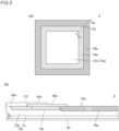
- Fig. 2 is a view for describing a semiconductor device 2 according to an embodiment 2.
- Fig. 2(a) is a plan view of the semiconductor device 2
- Fig. 2(b) is a cross-sectional view of the semiconductor device 2 taken along a line A2-A2 in Fig. 2(a).
- Fig. 2(b) may be also referred to as a cross-sectional view of a corner portion C2 in the semiconductor device 2. Also in Fig.
- the semiconductor device 2 according to the embodiment 2 has basically substantially the same configuration as the semiconductor device 1 according to the embodiment 1. However, the semiconductor device 2 according to the embodiment 2 differs from the semiconductor device 1 according to the embodiment 1 with respect to the shape of an outer edge of the second semiconductor region as viewed in a plan view.
- the outer edge of the second semiconductor region 16a is formed in a rectangular shape (a square shape). That is, as viewed in a plan view, an outer edge of a corner portion C2 of the second semiconductor region 16a has an angular shape.
- Fig. 3 is a view for describing the manner of extending a depletion layer at a corner portion of a semiconductor device.
- Fig. 3(a) is a plan view illustrating a corner portion C of the conventional semiconductor device 900
- Fig. 3(b) is a plan view illustrating the corner portion C2 of the semiconductor device 2 according to the embodiment 2.
- a first electrode, an insulation layer and a field plate disposed on a first main surface of a semiconductor base body are not illustrated.
- an outer edge of a corner portion C of the guard ring 916 is formed in an arc shape. Further, the outer edge of the guard ring 916 is disposed in contact with the n - -type semiconductor region 913 having lower concentration of dopants than the guard ring 916. Accordingly, when a reverse bias is applied to the semiconductor device 900, a depletion layer is liable to extend from an outer edge boundary of the guard ring 916 to an n - -type semiconductor region 913 side (outer side) (see a broken line D 1 in Fig. 3(a) ).
- an outer edge of the second semiconductor region 16a (guard ring) has a rectangular shape. Further, the outer edge of the second semiconductor region 16a is in contact with a third semiconductor region 18a having a larger total amount of dopants than the second semiconductor region 16a (usually, the concentration of dopants being also high). With such a configuration, when a reverse bias is applied, the depletion layer easily extends from an outer edge boundary of the second semiconductor region 16a toward a second semiconductor region 16a side (an inner side) (see a broken line D2 in Fig. 3 (b) ).
- the outer edge of the corner portion C1 of the second semiconductor region 16 has an arc shape.
- the outer edge of the second semiconductor region 16 is in contact with the third second semiconductor region 18 having a larger total amount of dopants than the second semiconductor region 16a.
- the depletion layer easily extends from an outer edge boundary of the second semiconductor region 16 toward a second semiconductor region 16 side (an inner side) and hence, different from the case of the conventional semiconductor device 900, spreading of the depletion layer is not obstructed even at a point that corresponds to 45° of the arc.
- an outer edge (a boundary between n - -type semiconductor region 13a and the second semiconductor region 16a) of the first semiconductor region 12a (n - -type semiconductor region 13a) is formed in a rectangular shape. Further, the outer edge of the second semiconductor region 16a is a boundary between the second semiconductor region 16a and the third semiconductor region 18a and hence, an inner edge of the third semiconductor region 18a is also formed in a shape that corresponds to the second semiconductor region 16a.
- the first electrode 20a, the insulation layer 30a, and the field plate 40a that are disposed on the first main surface are also formed in a shape that corresponds to the second semiconductor region 16a (the shape where the outer edge is formed in a rectangular shape as view in a plan view).
- the semiconductor device 2 according to the embodiment 2 differs from the semiconductor device 1 according to the embodiment 1 with respect to the shape of the outer edge of the second semiconductor region as viewed in a plan view.
- the semiconductor base body 10a has: the first semiconductor region 12a of a first conductive type; the second semiconductor region 16a of a second conductive type formed at the position where the first electrode 20a and the insulation layer 30a are in contact with each other; and a third semiconductor region 18a of a first conductive type formed in contact with the second semiconductor region 16a such that the third semiconductor region 18a surrounds the second semiconductor region 16a as viewed in a plan view, and assuming a total amount of dopants in the second semiconductor region 16a as S1 and a total amount of dopants in the third semiconductor region 18a as S2, the relationship of S1 ⁇ S2 is satisfied and hence, the combination of the second semiconductor region 16a and the third semiconductor region 18a has a function of a Zener diode.
- the semiconductor device 2 according to the embodiment 2 becomes a semiconductor device capable of having higher breakdown strength than the conventional semiconductor device in the same manner as the semiconductor device 1 according to the embodiment 1.
- an outer edge of the second semiconductor region 16a is formed in a rectangular shape (square shape). Accordingly, when a reverse bias is applied, a depletion layer easily extends from the corner portion of the second semiconductor region 16a and hence, a field strength at a vertex (a portion that corresponds to 45°) of the second semiconductor region 16a can be alleviated. As a result, in the semiconductor device 2 according to the embodiment 2, it is possible to generate an avalanche breakdown at a peripheral portion more easily than the corner portion C2 of the outer edge of the second semiconductor region 16a and hence, breakdown strength can be further increased.
- the semiconductor device 2 according to the embodiment 2 also acquires, in addition to the above-mentioned advantageous effects, the advantageous effects that the semiconductor device 1 according to the embodiment 1 possesses.
Landscapes
- Electrodes Of Semiconductors (AREA)
- Semiconductor Integrated Circuits (AREA)
Abstract
A semiconductor device 1 according to the present invention includes a semiconductor base body 10, a first electrode 20, and an insulation layer 30. The semiconductor base body 10 includes: a first semiconductor region 12 of a first conductive type (n-type); a second semiconductor region 16 of a second conductive type (p type) formed at a position where the second semiconductor region 16 is in contact with the first electrode 2o and the insulation layer 30; and a third semiconductor region 18 of a first conductive type (n-type) formed in contact with the second semiconductor region 16 such that the third semiconductor region 18 surrounds the second semiconductor region 16 as viewed in a plan view. In the semiconductor device 1, assuming a total amount of dopants in the second semiconductor region 16 as S1 and a total amount of dopants in the third semiconductor region 18 as S2, a relationship of S1<S2 is satisfied, and a combination of the second semiconductor region 16 and the third semiconductor region 18 has a function of a Zener diode.
According to the semiconductor device 1 of the present invention, it is possible to increase breakdown strength compared to a conventional semiconductor device.
According to the semiconductor device 1 of the present invention, it is possible to increase breakdown strength compared to a conventional semiconductor device.
Description
- The present invention relates to a semiconductor device.
- Conventionally, to acquire a high withstand voltage, there has been known a semiconductor device on which a so-called guard ring is formed (see patent literature 1).
-
Fig. 4 is a view for describing aconventional semiconductor device 900.Fig. 4(a) is a plan view of thesemiconductor device 900, andFig. 4(b) is a cross-sectional view of thesemiconductor device 900 taken along a line A-A inFig. 4(a). Fig.4(b) may be also referred to as a cross-sectional view of a corner portion C of thesemiconductor device 900. InFig. 4(a) , to indicate a shape of afirst semiconductor region 912 and a shape of aguard ring 916 as viewed in a plan view, afirst electrode 920, aninsulation layer 930 and afield plate 940 disposed on a first main surface of asemiconductor base body 910 are not illustrated. - As illustrated in
Fig. 4 , theconventional semiconductor device 900 includes: thesemiconductor base body 910, thefirst electrode 920 that is disposed on the first main surface of thesemiconductor base body 910, theinsulation layer 930 that is disposed on the first main surface so as to surround thefirst electrode 920 as viewed in a plan view, thefield plate 940 that is connected to thefirst electrode 920 and is disposed on theinsulation layer 930, and asecond electrode 950 that is disposed on a second main surface of thesemiconductor base body 910 on a side opposite to the first main surface. Thesemiconductor base body 910 has afirst semiconductor region 912 of an n-type (an n--type semiconductor region 913 and a n++-type semiconductor region 914), and theguard ring 916 of a p-type, and achannel stopper 918 of an n+-type that is spaced apart from theguard ring 916 and is disposed on an outer edge side of theguard ring 916. In theconventional semiconductor device 900, in general, an outer edge of the corner portion C of theguard ring 916 has been formed in an arc shape as viewed in a plan view (seeFig. 4(a) ). - Patent Literature 1:
JP-A-05-75100 - In the
conventional semiconductor device 900, there is a tendency that a contact edge E (a portion near a boundary between thefirst electrode 920 and theinsulation layer 920 in the semiconductor base body 910) is liable to be broken when a reverse bias is applied to the semiconductor device thus giving rise to a drawback that it is difficult for the semiconductor device to increase its breakdown strength. - The present invention has been made so as to overcome the above-mentioned drawback, and it is an object of the present invention to provide a semiconductor device capable of increasing breakdown strength thereof compared to the conventional semiconductor device.
- A semiconductor device according to the present invention includes: a semiconductor base body; a first electrode disposed on a first main surface of the semiconductor base body; and an insulation layer disposed on the first main surface such that the insulation layer surrounds the first electrode as viewed in a plan view, wherein the semiconductor base body includes: a first semiconductor region of a first conductive type; a second semiconductor region of a second conductive type that is formed at a position where the second semiconductor region is in contact with the first electrode and the insulation layer; and a third semiconductor region of the first conductive type that is formed in contact with the second semiconductor region so as to surround the second semiconductor region as viewed in a plan view, and assuming a total amount of dopants in the second semiconductor region as S1 and a total amount of dopants in the third semiconductor region as S2, a relationship of S1<S2 is satisfied, and a combination of the second semiconductor region and the third semiconductor region has a function of a Zener diode.
- According to the semiconductor device of the present invention, the semiconductor base body includes the third semiconductor region of the first conductive type that is formed in contact with the second semiconductor region so as to surround the second semiconductor region as viewed in a plan view, assuming the total amount of the dopants in the second semiconductor region as S1 and the total amount of dopants in the third semiconductor region as S2, the relationship of S1<S2 is satisfied, and the combination of the second semiconductor region and the third semiconductor region has a function of a Zener diode. Accordingly, when a reverse bias is applied to the semiconductor device, electric field strength between the second semiconductor region and the third semiconductor region becomes higher than electric field strength of a portion near a contact edge and hence, it is possible to generate an avalanche breakdown between the second semiconductor region and the third semiconductor region before the portion near the contact edge is broken. Accordingly, the semiconductor device according to the present invention becomes a semiconductor device capable of increasing breakdown strength compared to a conventional semiconductor device.
-
-
Fig. 1 is a view for describing asemiconductor device 1 according to anembodiment 1. -
Fig. 2 is a view for describing asemiconductor device 2 according to anembodiment 2. -
Fig. 3 is a view for describing the manner of extending of a depletion layer at a corner portion of a semiconductor device. -
Fig. 4 is a view for describing aconventional semiconductor device 900. - Hereinafter, a semiconductor device according to the present invention is described based on respective embodiments illustrated in drawings. The respective embodiments described hereinafter are not intended to limit the present invention according to claims.
- Further, it is not always the case that the constitutional elements described in the embodiments and all combinations of these constitutional elements are indispensable for the solutions to solve the problems of the present invention.
-
Fig. 1 is a view for describing asemiconductor device 1 according to anembodiment 1.Fig. 1(a) is a plan view of thesemiconductor device 1 andFig. 1(b) is a cross-sectional view of thesemiconductor device 1 taken along a line A1-A1 inFig. 1(a). Fig. 1(b) may be also referred to as a cross-sectional view of a corner portion C1 in thesemiconductor device 1. InFig. 1(a) , to illustrate the shapes of afirst semiconductor region 12, asecond semiconductor region 16 and athird semiconductor region 18 as viewed in a plan view, afirst electrode 20, aninsulation layer 30 and afield plate 40 that are disposed on a first main surface of asemiconductor base body 10 are not illustrated. - As illustrated in
Fig. 1 , thesemiconductor device 1 according to theembodiment 1 includes: thesemiconductor base body 10; thefirst electrode 20 that is disposed on the first main surface of thesemiconductor base body 10; theinsulation layer 30 that is disposed on the first main surface so as to surround thefirst electrode 20 as viewed in a plan view; thefield plate 40 that is connected to thefirst electrode 20 and is disposed above theinsulation layer 30; and asecond electrode 50 that is disposed on a second main surface of thesemiconductor base body 10 on a side opposite to the first main surface of thesemiconductor base body 10. Thesemiconductor device 1 illustrated inFig. 1 may further include constitutional elements besides the above-mentioned constitutional elements. Thesemiconductor device 1 is a Schottky barrier diode. - The
semiconductor base body 10 includes: afirst semiconductor region 12 of a first conductive type (n-type in the embodiment 1); asecond semiconductor region 16 of a second conductive type (p-type in the embodiment 1) and athird semiconductor region 18 of the first conductive type (n-type in the embodiment 1). The concentration of dopants in thethird semiconductor region 18 is higher than the concentration of dopants in an n--type semiconductor region 13 and lower than the concentration of dopants in an n++ -type semiconductor region 14 described later. Accordingly, inFig. 1 , "n+" is indicated in thethird semiconductor region 18. In thesemiconductor device 1, thesecond semiconductor region 16 may be also referred to as a guard ring, and thethird semiconductor region 18 may be also referred to as a channel stopper. - The
first semiconductor region 12 includes an n--type semiconductor region 13 disposed on a first main surface side, and an n++-type semiconductor region 14 disposed on a second main surface side. The wafer resistivity of the n--type semiconductor region 13 can be set to 0.6 to 25 Ωcm, for example. Further, a thickness of the n--type semiconductor region 13 can be set to 4 to 65 µm, for example. The concentration of dopants on the surface of an n++-type semiconductor region 14 can be set to 1×10²⁰ m-3 or more, for example. Further, a thickness of the n++-type semiconductor region 14 is set to 100 to 400 µm, for example. - The
second semiconductor region 16 is formed at the position where thefirst electrode 20 and theinsulation layer 30 are in contact with each other. In thesemiconductor device 1, as viewed in a plan view, an outer edge of the corner portion C1 of the second semiconductor region 16 (indicated by a symbol only with respect to the corner portion C1 disposed on a right upper portion of a surface of a sheet on whichFig. 1(a) is drawn) is formed in an arc shape. A total amount of dopants in thesecond semiconductor region 16 can be set to 3×10¹² to 8×1012 cm-2, for example. Further, a depth of thesecond semiconductor region 16 can be set 0.4 to 4.0 µm, for example. - In this specification, "a total amount of dopants" means a value obtained by integrating the concentration distribution of dopants in a depth direction from the surface. Although the total amount of dopants is a value relating to a dose amount (a doped amount of dopants), there may be a case where it is not always possible to acquire a proper correlation between a withstand voltage and a dose amount. This is because an amount of dopants is changeable depending on heat treatment or the like.
- The
third semiconductor region 18 is formed in contact with thesecond semiconductor region 16 such that thethird semiconductor region 18 surrounds thesecond semiconductor region 16 as viewed in a plan view. Thethird semiconductor region 18 is formed such that thethird semiconductor region 18 extends to an end portion of thesemiconductor device 1 as viewed in a plan view. Further, thethird semiconductor region 18 is formed to a depth deeper than the deepest portion of thesecond semiconductor region 16 from the first main surface. A total amount of dopants in thethird semiconductor region 18 may be set to 3×10¹² to 1×1015 cm-2, for example. The depth of thethird semiconductor region 18 can be set to 0.5 to 5.0 µm, for example. - In the
semiconductor device 1, assuming the total amount of dopants in thesecond semiconductor region 16 as S1 and the total amount of dopants in thethird semiconductor region 18 as S2, the relationship of S1 < S2 is satisfied. In thesemiconductor device 1, it is preferable that the relationship of 0.15 < (S1/S2) < 1 be satisfied. In thesemiconductor device 1, the combination of thesecond semiconductor region 16 and thethird semiconductor region 18 has a function of a Zener diode. - In this specification, "Zener diode" includes not only a Zener diode where Zener breakdown occurs on a p-n junction surface but also a Zener diode where an avalanche breakdown occurs depending on a condition.
- Hereinafter, advantageous effects acquired by the
semiconductor device 1 according to theembodiment 1 are described. - According to the
semiconductor device 1 of theembodiment 1, thesemiconductor base body 10 includes: thefirst semiconductor region 12 of a first conductive type; thesecond semiconductor region 16 of a second conductive type formed at the position where thefirst electrode 20 and theinsulation layer 30 are in contact with each other; and thethird semiconductor region 18 of the first conductive type formed in contact with thesecond semiconductor region 16 such that thethird semiconductor region 18 surrounds thesecond semiconductor region 16 as viewed in a plan view, and assuming the total amount of dopants in thesecond semiconductor region 16 as S1 and the total amount of dopants in thethird semiconductor region 18 as S2, the relationship of S1 < S2 is satisfied, and the combination of thesecond semiconductor region 16 and thethird semiconductor region 18 has a function of a Zener diode. Accordingly, when a reverse bias is applied to thesemiconductor device 1, it is possible to increase electric field strength between thesecond semiconductor region 16 and thethird semiconductor region 18 than electric field strength near a contact edge E1 and hence, it is possible to generate avalanche breakdown between thesecond semiconductor region 16 and thethird semiconductor region 18 before the contact edge E1 is broken. As a result, thesemiconductor device 1 according to theembodiment 1 becomes a semiconductor device having higher breakdown strength than a conventional semiconductor device. - Further, according to the
semiconductor device 1 of theembodiment 1, thethird semiconductor region 18 is formed to a depth deeper than the deepest portion of thesecond semiconductor region 16 from the first main surface and hence, it is possible to ensure a sufficient contact between thesecond semiconductor region 16 and thethird semiconductor region 18. - Further, according to the
semiconductor device 1 of theembodiment 1, the relationship of 0.15 < (S1/S2) < 1 is satisfied. Accordingly, a ratio of the total amount of dopants S1 in thesecond semiconductor region 16 with respect to the total amount of dopants S2 in thethird semiconductor region 18 can be increased to some extent and hence, it is possible to suppress lowering of a withstand voltage attributed to an excessively small amount of dopants in thesecond semiconductor region 16. - Further, the
semiconductor device 1 of theembodiment 1 forms a Schottky barrier diode that can increase breakdown strength compared to the prior art. -
Fig. 2 is a view for describing asemiconductor device 2 according to anembodiment 2.Fig. 2(a) is a plan view of thesemiconductor device 2, andFig. 2(b) is a cross-sectional view of thesemiconductor device 2 taken along a line A2-A2 inFig. 2(a). Fig. 2(b) may be also referred to as a cross-sectional view of a corner portion C2 in thesemiconductor device 2. Also inFig. 2(a) , to display shapes of afirst semiconductor region 12a, asecond semiconductor region 16a and athird semiconductor region 18a as viewed in a plan view, afirst electrode 20a, aninsulation layer 30a and afield plate 40a disposed on a first main surface of asemiconductor base body 10a are not illustrated. - The
semiconductor device 2 according to theembodiment 2 has basically substantially the same configuration as thesemiconductor device 1 according to theembodiment 1. However, thesemiconductor device 2 according to theembodiment 2 differs from thesemiconductor device 1 according to theembodiment 1 with respect to the shape of an outer edge of the second semiconductor region as viewed in a plan view. In thesemiconductor device 2 according to theembodiment 2, as viewed in a plan view, the outer edge of thesecond semiconductor region 16a is formed in a rectangular shape (a square shape). That is, as viewed in a plan view, an outer edge of a corner portion C2 of thesecond semiconductor region 16a has an angular shape. - In this
embodiment 2, a phenomenon obtained by forming the outer edge of thesecond semiconductor region 16a in a rectangular shape is described with reference toFig. 3. Fig. 3 is a view for describing the manner of extending a depletion layer at a corner portion of a semiconductor device.Fig. 3(a) is a plan view illustrating a corner portion C of theconventional semiconductor device 900, andFig. 3(b) is a plan view illustrating the corner portion C2 of thesemiconductor device 2 according to theembodiment 2. In the same manner as the cases described inFig. 2(a) andFig. 4(a) , also inFig. 3 , a first electrode, an insulation layer and a field plate disposed on a first main surface of a semiconductor base body are not illustrated. - First, in the
conventional semiconductor device 900, as illustrated inFig. 3(a) , as viewed in a plan view, an outer edge of a corner portion C of theguard ring 916 is formed in an arc shape. Further, the outer edge of theguard ring 916 is disposed in contact with the n--type semiconductor region 913 having lower concentration of dopants than theguard ring 916. Accordingly, when a reverse bias is applied to thesemiconductor device 900, a depletion layer is liable to extend from an outer edge boundary of theguard ring 916 to an n--type semiconductor region 913 side (outer side) (see a broken line D1 inFig. 3(a) ). At this stage of the operation, in view of a charge balance, spreading of the depletion layer is liable to become narrow at a point that corresponds to 45° of an arc (see point P1 inFig. 3(a) ) (see double-headed arrow inFig. 3(a) ). Accordingly, in theconventional semiconductor device 900, electric field strength is liable to be concentrated near such a point. - On the other hand, in the
semiconductor device 2 according to theembodiment 2, as illustrated inFig.3 (b) , as viewed in a plan view, an outer edge of thesecond semiconductor region 16a (guard ring) has a rectangular shape. Further, the outer edge of thesecond semiconductor region 16a is in contact with athird semiconductor region 18a having a larger total amount of dopants than thesecond semiconductor region 16a (usually, the concentration of dopants being also high). With such a configuration, when a reverse bias is applied, the depletion layer easily extends from an outer edge boundary of thesecond semiconductor region 16a toward asecond semiconductor region 16a side (an inner side) (see a broken line D2 inFig. 3 (b) ). With such a shallow junction, in view of the relationship of a charge balance of an interface, spreading of the depletion layer is accelerated in a vertex (a portion corresponding to 45°, a point P2 inFig. 3(b) ) of thesecond semiconductor region 16a (see double-headed arrow inFig. 3(b) ). Accordingly, in thesemiconductor device 2 of theembodiment 2, electric field strength can be alleviated near such a point. - In the
semiconductor device 1 according to theembodiment 1, the outer edge of the corner portion C1 of thesecond semiconductor region 16 has an arc shape. However, different from the case of theconventional semiconductor device 900, the outer edge of thesecond semiconductor region 16 is in contact with the thirdsecond semiconductor region 18 having a larger total amount of dopants than thesecond semiconductor region 16a. In this case, the depletion layer easily extends from an outer edge boundary of thesecond semiconductor region 16 toward asecond semiconductor region 16 side (an inner side) and hence, different from the case of theconventional semiconductor device 900, spreading of the depletion layer is not obstructed even at a point that corresponds to 45° of the arc. - In the
semiconductor device 2, an outer edge (a boundary between n--type semiconductor region 13a and thesecond semiconductor region 16a) of thefirst semiconductor region 12a (n--type semiconductor region 13a) is formed in a rectangular shape. Further, the outer edge of thesecond semiconductor region 16a is a boundary between thesecond semiconductor region 16a and thethird semiconductor region 18a and hence, an inner edge of thethird semiconductor region 18a is also formed in a shape that corresponds to thesecond semiconductor region 16a. Although the illustration as view in a plan view is omitted, thefirst electrode 20a, theinsulation layer 30a, and thefield plate 40a that are disposed on the first main surface are also formed in a shape that corresponds to thesecond semiconductor region 16a (the shape where the outer edge is formed in a rectangular shape as view in a plan view). - The
semiconductor device 2 according to theembodiment 2 differs from thesemiconductor device 1 according to theembodiment 1 with respect to the shape of the outer edge of the second semiconductor region as viewed in a plan view. However, according to thesemiconductor device 2, thesemiconductor base body 10a has: thefirst semiconductor region 12a of a first conductive type; thesecond semiconductor region 16a of a second conductive type formed at the position where thefirst electrode 20a and theinsulation layer 30a are in contact with each other; and athird semiconductor region 18a of a first conductive type formed in contact with thesecond semiconductor region 16a such that thethird semiconductor region 18a surrounds thesecond semiconductor region 16a as viewed in a plan view, and assuming a total amount of dopants in thesecond semiconductor region 16a as S1 and a total amount of dopants in thethird semiconductor region 18a as S2, the relationship of S1<S2 is satisfied and hence, the combination of thesecond semiconductor region 16a and thethird semiconductor region 18a has a function of a Zener diode. Accordingly, when a reverse bias is applied, electric field strength between thesecond semiconductor region 16a and thethird semiconductor region 18a becomes larger than a field strength near a contact edge E2 and hence, it is possible to generate an avalanche breakdown between thesecond semiconductor region 16a and thethird semiconductor region 18a before the contact edge E2 is broken. As a result, thesemiconductor device 2 according to theembodiment 2 becomes a semiconductor device capable of having higher breakdown strength than the conventional semiconductor device in the same manner as thesemiconductor device 1 according to theembodiment 1. - Further, according to the
semiconductor device 2 of theembodiment 2, as viewed in a plan view, an outer edge of thesecond semiconductor region 16a is formed in a rectangular shape (square shape). Accordingly, when a reverse bias is applied, a depletion layer easily extends from the corner portion of thesecond semiconductor region 16a and hence, a field strength at a vertex (a portion that corresponds to 45°) of thesecond semiconductor region 16a can be alleviated. As a result, in thesemiconductor device 2 according to theembodiment 2, it is possible to generate an avalanche breakdown at a peripheral portion more easily than the corner portion C2 of the outer edge of thesecond semiconductor region 16a and hence, breakdown strength can be further increased. - The
semiconductor device 2 according to theembodiment 2 also acquires, in addition to the above-mentioned advantageous effects, the advantageous effects that thesemiconductor device 1 according to theembodiment 1 possesses. - Although the present invention has been described based on the above-mentioned respective embodiments, the present invention is not limited to the above-mentioned respective embodiments. The present invention can be carried out in various modes without departing from the gist of the present invention. For example, the following modifications are conceivable.
-
- (1) The positions, the sizes and the like described in the above-mentioned respective embodiments (also including the respective modifications described hereinafter) are provided for an exemplifying purpose, and can be changed provided that the advantageous effects of the present invention are not impaired.
- (2) In the above-mentioned respective embodiments, the
semiconductor devices - (3) In the
semiconductor device 2 according to the above-mentionedembodiment 2, as viewed in a plan view, the outer edge of thesecond semiconductor region 16a is formed in a square shape. However, the present invention is not limited to such a configuration. The outer edge of the second semiconductor region may be formed in a rectangular shape. -
- 1, 2: semiconductor device
- 10, 10a: semiconductor base body
- 12, 12a: first semiconductor region
- 13, 13a: n--semiconductor region
- 14: n+-semiconductor region
- 16, 16a: second semiconductor region
- 18, 18a: third semiconductor region
- 20, 20a: first electrode
- 30, 30a: insulation layer
- 40, 40a: field plate
- 50: second electrode
- C1, C2: corner portions
- E1, E2: contact edge
Claims (5)
- A semiconductor device comprising:a semiconductor base body;a first electrode disposed on a first main surface of the semiconductor base body; andan insulation layer disposed on the first main surface such that the insulation layer surrounds the first electrode as viewed in a plan view, whereinthe semiconductor base body includes: a first semiconductor region of a first conductive type; a second semiconductor region of a second conductive type that is formed at a position where the second semiconductor region is in contact with the first electrode and the insulation layer; and a third semiconductor region of the first conductive type that is formed in contact with the second semiconductor region so as to surround the second semiconductor region as viewed in a plan view, andassuming a total amount of dopants in the second semiconductor region as S1 and a total amount of dopants in the third semiconductor region as S2, a relationship of S1<S2 is satisfied, anda combination of the second semiconductor region and the third semiconductor region has a function of a Zener diode.
- The semiconductor device according to claim 1, wherein the third semiconductor region is formed to a depth deeper than a deepest portion of the second semiconductor region from the first main surface.
- The semiconductor device according to claim 1, wherein a relationship of 0.15<(S1/S2)<1 is satisfied.
- The semiconductor device according to claim 1, wherein an outer edge of the second semiconductor region is formed in a rectangular shape as viewed in a plan view.
- The semiconductor device according to claim 1, wherein the semiconductor device is a Schottky barrier diode.
Applications Claiming Priority (2)
| Application Number | Priority Date | Filing Date | Title |
|---|---|---|---|
| JP2022097839A JP2023183979A (en) | 2022-06-17 | 2022-06-17 | semiconductor equipment |
| PCT/JP2023/021390 WO2023243537A1 (en) | 2022-06-17 | 2023-06-08 | Semiconductor device |
Publications (1)
| Publication Number | Publication Date |
|---|---|
| EP4542656A1 true EP4542656A1 (en) | 2025-04-23 |
Family
ID=89191170
Family Applications (1)
| Application Number | Title | Priority Date | Filing Date |
|---|---|---|---|
| EP23823828.1A Pending EP4542656A1 (en) | 2022-06-17 | 2023-06-08 | Semiconductor device |
Country Status (7)
| Country | Link |
|---|---|
| US (1) | US20250338524A1 (en) |
| EP (1) | EP4542656A1 (en) |
| JP (1) | JP2023183979A (en) |
| CN (1) | CN119302050A (en) |
| NL (1) | NL2035068B1 (en) |
| TW (1) | TWI861879B (en) |
| WO (1) | WO2023243537A1 (en) |
Families Citing this family (2)
| Publication number | Priority date | Publication date | Assignee | Title |
|---|---|---|---|---|
| JP7801676B2 (en) * | 2020-11-06 | 2026-01-19 | パナソニックIpマネジメント株式会社 | Biometric information acquisition device |
| WO2025163928A1 (en) * | 2024-01-31 | 2025-08-07 | 新電元工業株式会社 | Semiconductor device |
Family Cites Families (10)
| Publication number | Priority date | Publication date | Assignee | Title |
|---|---|---|---|---|
| JPS54141578A (en) * | 1978-04-25 | 1979-11-02 | Nec Corp | Semiconductor device |
| JPS61166164A (en) * | 1985-01-18 | 1986-07-26 | Sanyo Electric Co Ltd | Shock barrier semiconductor device |
| JP3117506B2 (en) | 1991-09-13 | 2000-12-18 | 株式会社日立製作所 | Semiconductor rectifier |
| DE19853743C2 (en) * | 1998-11-21 | 2000-10-12 | Micronas Intermetall Gmbh | Semiconductor component with at least one Zener diode and at least one Schottky diode connected in parallel thereto, and method for producing the semiconductor components |
| US6462393B2 (en) * | 2001-03-20 | 2002-10-08 | Fabtech, Inc. | Schottky device |
| JP4827386B2 (en) * | 2004-06-17 | 2011-11-30 | 日本インター株式会社 | Schottky barrier diode |
| WO2009116444A1 (en) * | 2008-03-17 | 2009-09-24 | 三菱電機株式会社 | Semiconductor device |
| EP2677540A1 (en) * | 2012-06-19 | 2013-12-25 | Nxp B.V. | Electronic device and method of manufacturing the same |
| JP2017017309A (en) * | 2015-04-14 | 2017-01-19 | ローム株式会社 | diode |
| CN113646895B (en) * | 2019-04-11 | 2024-07-05 | 三菱电机株式会社 | Semiconductor device and power conversion device |
-
2022
- 2022-06-17 JP JP2022097839A patent/JP2023183979A/en active Pending
-
2023
- 2023-05-16 TW TW112118200A patent/TWI861879B/en active
- 2023-06-08 EP EP23823828.1A patent/EP4542656A1/en active Pending
- 2023-06-08 US US18/871,477 patent/US20250338524A1/en active Pending
- 2023-06-08 WO PCT/JP2023/021390 patent/WO2023243537A1/en not_active Ceased
- 2023-06-08 CN CN202380043567.4A patent/CN119302050A/en active Pending
- 2023-06-12 NL NL2035068A patent/NL2035068B1/en active
Also Published As
| Publication number | Publication date |
|---|---|
| TWI861879B (en) | 2024-11-11 |
| US20250338524A1 (en) | 2025-10-30 |
| WO2023243537A1 (en) | 2023-12-21 |
| CN119302050A (en) | 2025-01-10 |
| TW202401827A (en) | 2024-01-01 |
| NL2035068A (en) | 2024-01-04 |
| NL2035068B1 (en) | 2025-05-22 |
| JP2023183979A (en) | 2023-12-28 |
Similar Documents
| Publication | Publication Date | Title |
|---|---|---|
| CN106531813B (en) | semiconductor device | |
| EP2498292B1 (en) | Schottky barrier diode | |
| US9147758B2 (en) | Semiconductor device | |
| US10566464B2 (en) | Semiconductor device | |
| US20250338524A1 (en) | Semiconductor device | |
| US8476673B2 (en) | Diode | |
| US11101345B2 (en) | Semiconductor device | |
| US7960754B2 (en) | Diode having high breakdown voltage and low on-resistance | |
| JP2018060984A (en) | Semiconductor device | |
| CN104779290A (en) | Semiconductor device | |
| US8686515B2 (en) | Double-groove bidirectional vertical component | |
| JP7249921B2 (en) | semiconductor equipment | |
| US11901407B2 (en) | Semiconductor device with improved junction termination extension region | |
| EP3457442B1 (en) | Semiconductor device | |
| US7535075B2 (en) | Semiconductor device | |
| EP4411821A1 (en) | Terminal structure, manufacturing method and power device | |
| CN216054719U (en) | Semiconductor structure | |
| US20120161198A1 (en) | Bidirectional shockley diode with extended mesa | |
| EP3726586A1 (en) | Wide-gap semiconductor device | |
| US20160126308A1 (en) | Super-junction edge termination for power devices | |
| CN113629132A (en) | Semiconductor structure and forming method thereof | |
| US20250311336A1 (en) | Semiconductor device | |
| US20240021681A1 (en) | Semiconductor device | |
| US20260082642A1 (en) | Semiconductor device | |
| WO2025163928A1 (en) | Semiconductor device |
Legal Events
| Date | Code | Title | Description |
|---|---|---|---|
| STAA | Information on the status of an ep patent application or granted ep patent |
Free format text: STATUS: THE INTERNATIONAL PUBLICATION HAS BEEN MADE |
|
| PUAI | Public reference made under article 153(3) epc to a published international application that has entered the european phase |
Free format text: ORIGINAL CODE: 0009012 |
|
| STAA | Information on the status of an ep patent application or granted ep patent |
Free format text: STATUS: REQUEST FOR EXAMINATION WAS MADE |
|
| 17P | Request for examination filed |
Effective date: 20241205 |
|
| AK | Designated contracting states |
Kind code of ref document: A1 Designated state(s): AL AT BE BG CH CY CZ DE DK EE ES FI FR GB GR HR HU IE IS IT LI LT LU LV MC ME MK MT NL NO PL PT RO RS SE SI SK SM TR |
|
| DAV | Request for validation of the european patent (deleted) | ||
| DAX | Request for extension of the european patent (deleted) |