EP4542655A1 - Semiconductor device and method for manufacturing semiconductor device - Google Patents
Semiconductor device and method for manufacturing semiconductor device Download PDFInfo
- Publication number
- EP4542655A1 EP4542655A1 EP23823548.5A EP23823548A EP4542655A1 EP 4542655 A1 EP4542655 A1 EP 4542655A1 EP 23823548 A EP23823548 A EP 23823548A EP 4542655 A1 EP4542655 A1 EP 4542655A1
- Authority
- EP
- European Patent Office
- Prior art keywords
- nitride semiconductor
- semiconductor layer
- layer
- type gan
- semiconductor device
- Prior art date
- Legal status (The legal status is an assumption and is not a legal conclusion. Google has not performed a legal analysis and makes no representation as to the accuracy of the status listed.)
- Pending
Links
Images











Classifications
-
- H—ELECTRICITY
- H10—SEMICONDUCTOR DEVICES; ELECTRIC SOLID-STATE DEVICES NOT OTHERWISE PROVIDED FOR
- H10P—GENERIC PROCESSES OR APPARATUS FOR THE MANUFACTURE OR TREATMENT OF DEVICES COVERED BY CLASS H10
- H10P14/00—Formation of materials, e.g. in the shape of layers or pillars
- H10P14/20—Formation of materials, e.g. in the shape of layers or pillars of semiconductor materials
- H10P14/32—Formation of materials, e.g. in the shape of layers or pillars of semiconductor materials characterised by intermediate layers between substrates and deposited layers
- H10P14/3202—Materials thereof
- H10P14/3214—Materials thereof being Group IIIA-VA semiconductors
- H10P14/3216—Nitrides
-
- H—ELECTRICITY
- H10—SEMICONDUCTOR DEVICES; ELECTRIC SOLID-STATE DEVICES NOT OTHERWISE PROVIDED FOR
- H10D—INORGANIC ELECTRIC SEMICONDUCTOR DEVICES
- H10D62/00—Semiconductor bodies, or regions thereof, of devices having potential barriers
- H10D62/60—Impurity distributions or concentrations
-
- H—ELECTRICITY
- H10—SEMICONDUCTOR DEVICES; ELECTRIC SOLID-STATE DEVICES NOT OTHERWISE PROVIDED FOR
- H10D—INORGANIC ELECTRIC SEMICONDUCTOR DEVICES
- H10D30/00—Field-effect transistors [FET]
- H10D30/01—Manufacture or treatment
- H10D30/015—Manufacture or treatment of FETs having heterojunction interface channels or heterojunction gate electrodes, e.g. HEMT
-
- H—ELECTRICITY
- H10—SEMICONDUCTOR DEVICES; ELECTRIC SOLID-STATE DEVICES NOT OTHERWISE PROVIDED FOR
- H10D—INORGANIC ELECTRIC SEMICONDUCTOR DEVICES
- H10D30/00—Field-effect transistors [FET]
- H10D30/01—Manufacture or treatment
- H10D30/061—Manufacture or treatment of FETs having Schottky gates
-
- H—ELECTRICITY
- H10—SEMICONDUCTOR DEVICES; ELECTRIC SOLID-STATE DEVICES NOT OTHERWISE PROVIDED FOR
- H10D—INORGANIC ELECTRIC SEMICONDUCTOR DEVICES
- H10D30/00—Field-effect transistors [FET]
- H10D30/40—FETs having zero-dimensional [0D], one-dimensional [1D] or two-dimensional [2D] charge carrier gas channels
- H10D30/47—FETs having zero-dimensional [0D], one-dimensional [1D] or two-dimensional [2D] charge carrier gas channels having two-dimensional [2D] charge carrier gas channels, e.g. nanoribbon FETs or high electron mobility transistors [HEMT]
- H10D30/471—High electron mobility transistors [HEMT] or high hole mobility transistors [HHMT]
- H10D30/472—High electron mobility transistors [HEMT] or high hole mobility transistors [HHMT] having lower bandgap active layer formed on top of wider bandgap layer, e.g. inverted HEMT
-
- H—ELECTRICITY
- H10—SEMICONDUCTOR DEVICES; ELECTRIC SOLID-STATE DEVICES NOT OTHERWISE PROVIDED FOR
- H10D—INORGANIC ELECTRIC SEMICONDUCTOR DEVICES
- H10D30/00—Field-effect transistors [FET]
- H10D30/40—FETs having zero-dimensional [0D], one-dimensional [1D] or two-dimensional [2D] charge carrier gas channels
- H10D30/47—FETs having zero-dimensional [0D], one-dimensional [1D] or two-dimensional [2D] charge carrier gas channels having two-dimensional [2D] charge carrier gas channels, e.g. nanoribbon FETs or high electron mobility transistors [HEMT]
- H10D30/471—High electron mobility transistors [HEMT] or high hole mobility transistors [HHMT]
- H10D30/475—High electron mobility transistors [HEMT] or high hole mobility transistors [HHMT] having wider bandgap layer formed on top of lower bandgap active layer, e.g. undoped barrier HEMTs such as i-AlGaN/GaN HEMTs
-
- H—ELECTRICITY
- H10—SEMICONDUCTOR DEVICES; ELECTRIC SOLID-STATE DEVICES NOT OTHERWISE PROVIDED FOR
- H10D—INORGANIC ELECTRIC SEMICONDUCTOR DEVICES
- H10D62/00—Semiconductor bodies, or regions thereof, of devices having potential barriers
- H10D62/10—Shapes, relative sizes or dispositions of the regions of the semiconductor bodies; Shapes of the semiconductor bodies
- H10D62/124—Shapes, relative sizes or dispositions of the regions of semiconductor bodies or of junctions between the regions
-
- H—ELECTRICITY
- H10—SEMICONDUCTOR DEVICES; ELECTRIC SOLID-STATE DEVICES NOT OTHERWISE PROVIDED FOR
- H10D—INORGANIC ELECTRIC SEMICONDUCTOR DEVICES
- H10D62/00—Semiconductor bodies, or regions thereof, of devices having potential barriers
- H10D62/10—Shapes, relative sizes or dispositions of the regions of the semiconductor bodies; Shapes of the semiconductor bodies
- H10D62/13—Semiconductor regions connected to electrodes carrying current to be rectified, amplified or switched, e.g. source or drain regions
- H10D62/149—Source or drain regions of field-effect devices
- H10D62/151—Source or drain regions of field-effect devices of IGFETs
-
- H—ELECTRICITY
- H10—SEMICONDUCTOR DEVICES; ELECTRIC SOLID-STATE DEVICES NOT OTHERWISE PROVIDED FOR
- H10D—INORGANIC ELECTRIC SEMICONDUCTOR DEVICES
- H10D62/00—Semiconductor bodies, or regions thereof, of devices having potential barriers
- H10D62/80—Semiconductor bodies, or regions thereof, of devices having potential barriers characterised by the materials
- H10D62/82—Heterojunctions
- H10D62/824—Heterojunctions comprising only Group III-V materials heterojunctions, e.g. GaN/AlGaN heterojunctions
-
- H—ELECTRICITY
- H10—SEMICONDUCTOR DEVICES; ELECTRIC SOLID-STATE DEVICES NOT OTHERWISE PROVIDED FOR
- H10D—INORGANIC ELECTRIC SEMICONDUCTOR DEVICES
- H10D64/00—Electrodes of devices having potential barriers
- H10D64/20—Electrodes characterised by their shapes, relative sizes or dispositions
- H10D64/27—Electrodes not carrying the current to be rectified, amplified, oscillated or switched, e.g. gates
- H10D64/311—Gate electrodes for field-effect devices
- H10D64/411—Gate electrodes for field-effect devices for FETs
- H10D64/511—Gate electrodes for field-effect devices for FETs for IGFETs
- H10D64/517—Gate electrodes for field-effect devices for FETs for IGFETs characterised by the conducting layers
- H10D64/518—Gate electrodes for field-effect devices for FETs for IGFETs characterised by the conducting layers characterised by their lengths or sectional shapes
-
- H—ELECTRICITY
- H10—SEMICONDUCTOR DEVICES; ELECTRIC SOLID-STATE DEVICES NOT OTHERWISE PROVIDED FOR
- H10P—GENERIC PROCESSES OR APPARATUS FOR THE MANUFACTURE OR TREATMENT OF DEVICES COVERED BY CLASS H10
- H10P14/00—Formation of materials, e.g. in the shape of layers or pillars
- H10P14/20—Formation of materials, e.g. in the shape of layers or pillars of semiconductor materials
- H10P14/29—Formation of materials, e.g. in the shape of layers or pillars of semiconductor materials characterised by the substrates
- H10P14/2901—Materials
- H10P14/2902—Materials being Group IVA materials
- H10P14/2904—Silicon carbide
-
- H—ELECTRICITY
- H10—SEMICONDUCTOR DEVICES; ELECTRIC SOLID-STATE DEVICES NOT OTHERWISE PROVIDED FOR
- H10P—GENERIC PROCESSES OR APPARATUS FOR THE MANUFACTURE OR TREATMENT OF DEVICES COVERED BY CLASS H10
- H10P14/00—Formation of materials, e.g. in the shape of layers or pillars
- H10P14/20—Formation of materials, e.g. in the shape of layers or pillars of semiconductor materials
- H10P14/32—Formation of materials, e.g. in the shape of layers or pillars of semiconductor materials characterised by intermediate layers between substrates and deposited layers
- H10P14/3242—Structure
- H10P14/3244—Layer structure
- H10P14/3251—Layer structure consisting of three or more layers
- H10P14/3252—Alternating layers, e.g. superlattice
-
- H—ELECTRICITY
- H10—SEMICONDUCTOR DEVICES; ELECTRIC SOLID-STATE DEVICES NOT OTHERWISE PROVIDED FOR
- H10P—GENERIC PROCESSES OR APPARATUS FOR THE MANUFACTURE OR TREATMENT OF DEVICES COVERED BY CLASS H10
- H10P14/00—Formation of materials, e.g. in the shape of layers or pillars
- H10P14/20—Formation of materials, e.g. in the shape of layers or pillars of semiconductor materials
- H10P14/34—Deposited materials, e.g. layers
- H10P14/3402—Deposited materials, e.g. layers characterised by the chemical composition
- H10P14/3414—Deposited materials, e.g. layers characterised by the chemical composition being group IIIA-VIA materials
- H10P14/3416—Nitrides
-
- H—ELECTRICITY
- H10—SEMICONDUCTOR DEVICES; ELECTRIC SOLID-STATE DEVICES NOT OTHERWISE PROVIDED FOR
- H10P—GENERIC PROCESSES OR APPARATUS FOR THE MANUFACTURE OR TREATMENT OF DEVICES COVERED BY CLASS H10
- H10P14/00—Formation of materials, e.g. in the shape of layers or pillars
- H10P14/20—Formation of materials, e.g. in the shape of layers or pillars of semiconductor materials
- H10P14/34—Deposited materials, e.g. layers
- H10P14/3438—Doping during depositing
- H10P14/3441—Conductivity type
- H10P14/3442—N-type
-
- H—ELECTRICITY
- H10—SEMICONDUCTOR DEVICES; ELECTRIC SOLID-STATE DEVICES NOT OTHERWISE PROVIDED FOR
- H10D—INORGANIC ELECTRIC SEMICONDUCTOR DEVICES
- H10D62/00—Semiconductor bodies, or regions thereof, of devices having potential barriers
- H10D62/40—Crystalline structures
- H10D62/405—Orientations of crystalline planes
-
- H—ELECTRICITY
- H10—SEMICONDUCTOR DEVICES; ELECTRIC SOLID-STATE DEVICES NOT OTHERWISE PROVIDED FOR
- H10D—INORGANIC ELECTRIC SEMICONDUCTOR DEVICES
- H10D62/00—Semiconductor bodies, or regions thereof, of devices having potential barriers
- H10D62/80—Semiconductor bodies, or regions thereof, of devices having potential barriers characterised by the materials
- H10D62/85—Semiconductor bodies, or regions thereof, of devices having potential barriers characterised by the materials being Group III-V materials, e.g. GaAs
- H10D62/8503—Nitride Group III-V materials, e.g. AlN or GaN
Definitions
- the present disclosure relates to semiconductor devices and methods for manufacturing semiconductor devices.
- a structure in which a nitride semiconductor layer including a high concentration of an impurity is regrown has been proposed, in order to reduce a contact resistance or the like in a semiconductor device using a nitride semiconductor.
- NON-PATENT DOCUMENT 1 Applied Physics Express, 2 (2009) 051001
- a semiconductor device includes a first nitride semiconductor layer including gallium, and a second nitride semiconductor layer formed on the first nitride semiconductor layer and including gallium, wherein the second nitride semiconductor layer includes a plurality of third nitride semiconductor layers and a plurality of fourth nitride semiconductor layers alternately laminated on the first nitride semiconductor layer, the plurality of third nitride semiconductor layers include an impurity of a first conductivity type with a first concentration, the plurality of fourth nitride semiconductor layers include the impurity of the first conductivity type with a second concentration higher than the first concentration, and the first concentration is 1 ⁇ 10 20 cm -3 or higher.
- One object of the present disclosure is to provide a semiconductor device and a method for manufacturing the semiconductor device, which can reduce deterioration of the electrical characteristics caused by the precipitation of the impurity element.
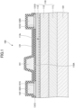
- FIG. 1 is a cross sectional view illustrating the semiconductor device according to the first embodiment.
- HEMT high electron mobility transistor
- a semiconductor device 100 mainly includes a substrate 101, a nitride semiconductor layer 110, an insulating layer 121, an n-type gallium nitride (GaN) layer 131S, an n-type GaN layer 131D, a gate electrode 141, a source electrode 132S, a drain electrode 132D, and an insulating layer 142.
- a substrate 101 a nitride semiconductor layer 110, an insulating layer 121, an n-type gallium nitride (GaN) layer 131S, an n-type GaN layer 131D, a gate electrode 141, a source electrode 132S, a drain electrode 132D, and an insulating layer 142.
- GaN gallium nitride
- the substrate 101 is a substrate for growing a GaN-based semiconductor, for example, and is a semiinsulating silicon carbide (SiC) substrate, for example.
- SiC silicon carbide
- a front surface of the substrate 101 is a carbon (C) polar surface.
- the nitride semiconductor layer 110 can undergo crystal growth using a nitrogen (N) polar surface as a growth surface.
- a sapphire substrate may be used as the substrate for growing the GaN-based semiconductor.
- the substrate 101 does not have to be the substrate for crystal growth, and in this case, the nitride semiconductor layer 110 may be grown on another substrate, and after removing this other substrate from the nitride semiconductor layer 110, the substrate 101 may be bonded to the nitride semiconductor layer 110.
- a semiinsulating substrate made of various materials, such as a sapphire substrate, a silicon (Si) substrate, a SiC substrate, an aluminum nitride (AlN) substrate, a sintered body, or the like, for example, may be used as the substrate 101.
- the nitride semiconductor layer 110 includes a buffer layer 111, a barrier layer 112, and a channel layer 113.
- the nitride semiconductor layer 110 is an example of a first nitride semiconductor layer.
- the buffer layer 111 is an AlN layer, for example.
- a thickness of the AlN layer is 5 nm or greater and 100 nm or less, for example.
- the buffer layer 111 may include an AlN layer, and a GaN layer or an aluminum gallium nitride (AlGaN) layer on the AlN layer.
- a thickness of the GaN layer or the AlGaN layer is 300 nm or greater and 2000 nm or less, for example.
- the barrier layer 112 is an AlGaN layer, for example.
- a band gap of the barrier layer 112 is larger than a band gap of the channel layer 113 which will be described later.
- a thickness of the barrier layer 112 is in a range of 5 nm or greater and 50 nm or less, for example, and is 30 nm in one embodiment.
- an Al composition x thereof is 0.15 or greater and 0.55 or less, for example, and is 0.35 in one embodiment.
- a conductivity type of the barrier layer 112 is an n-type or undoped (i-type), for example.
- An indium aluminum nitride (InAlN) layer or an indium aluminum gallium nitride (InAlGaN) layer may be used in place of the AlGaN layer.
- the channel layer 113 is a GaN layer, for example.
- the band gap of the channel layer 113 is smaller than the band gap of the barrier layer 112.
- a thickness of the channel layer 113 is in a range of 5 nm or greater and 30 nm or less, for example, and is 9 nm in one embodiment.
- a strain is generated between the channel layer 113 and the barrier layer 112 due to a difference in lattice constants thereof, and this strain induces a piezoelectric charge at an interface between the two layers.
- a two-dimensional electron gas (2DEG) is generated in a region of the channel layer 113 closer to the barrier layer 112, thereby forming a channel region 113c.
- a conductivity type of the channel layer 113 is the n-type or undoped (i-type), for example.
- a front surface of the channel layer 113 constitutes a front surface 110A of the nitride semiconductor layer 110.
- a spacer layer may be formed between the barrier layer 112 and the channel layer 113.
- the spacer layer is an AlN layer, for example.
- a thicknesses of the spacer layer is in a range of 0.5 nm or greater and 3.0 nm or less, for example, and is 1.0 nm in one embodiment.
- the buffer layer 111, the barrier layer 112, and the channel layer 113 undergo crystal growth using the N polar surface as the growth surface. Accordingly, front surfaces of the buffer layer 111, the barrier layer 112, and the channel layer 113 opposite to back surfaces thereof facing the substrate 101 become N polar surfaces, and the back surfaces thereof facing the substrate 101 become gallium (Ga) polar surfaces.
- the insulating layer 121 makes contact with the front surface 110A of the nitride semiconductor layer 110.
- the insulating layer 121 is a silicon nitride (SiN) layer, for example. Openings 121S and 121D are formed in the insulating layer 121. A portion of the nitride semiconductor layer 110 is exposed via the opening 121S, and another portion of the nitride semiconductor layer 110 is exposed via the opening 121D.
- the n-type GaN layer 131S is formed on the nitride semiconductor layer 110 inside the opening 121S.
- the n-type GaN layer 131D is formed on the nitride semiconductor layer 110 inside the opening 121D.
- the n-type GaN layers 131S and 131D include germanium (Ge) or Si as an n-type impurity.
- the n-type GaN layers 131S and 131D are examples of a second nitride semiconductor layer.
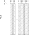
- FIG. 2 is a cross sectional view illustrating the n-type GaN layers 131S and 131D in the first embodiment.
- FIG. 3 is a diagram illustrating a relationship between a depth from front surfaces of the n-type GaN layers 131S and 131D and an impurity concentration in the first embodiment.
- the n-type GaN layers 131S and 131D which are examples of the second nitride semiconductor layer, include a plurality of n-type GaN layers 150 and a plurality of n-type GaN layers 160.
- the n-type GaN layers 150 and 160 are alternately laminated on the nitride semiconductor layer 110.
- the n-type GaN layers 150 and 160 are laminated on the nitride semiconductor layer 110 with a period of 8 nm or less.
- the n-type GaN layer 150 includes an n-type impurity with a first concentration of 1 ⁇ 10 20 cm -3 or higher.
- the n-type GaN layers 131S and 131D have the n-type GaN layer 150 as a lowermost layer and the n-type GaN layer 160 as an uppermost layer, for example.
- the n-type GaN layer 150 is an example of a third nitride semiconductor layer
- the n-type GaN layer 160 is an example of a fourth nitride semiconductor layer.
- the source electrode 132S is formed on the n-type GaN layer 131S
- the drain electrode 132D is formed on the n-type GaN layer 131D.
- the source electrode 132S and the drain electrode 132D include a laminated structure in which a tantalum (Ta) film, an Al film, and a Ta film are laminated in this order, for example.
- the source electrode 132S and the drain electrode 132D may include a laminated structure in which a titanium (Ti) film, an Al film, and a Ti film are laminated in this order, or a laminated structure in which a nickel (Ni) film and a gold (Au) film are laminated in this order, for example.
- the source electrode 132S and the drain electrode 132D are examples of an ohmic electrode.
- the gate electrode 141 is formed on the insulating layer 121 between the source electrode 132S and the drain electrode 132D.
- the gate electrode 141 includes a laminated structure in which a Ni film, a palladium (Pd) film, and an Au film are laminated in this order, for example.
- the insulating layer 142 is formed on the insulating layer 121, and covers the gate electrode 141.
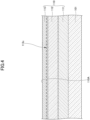
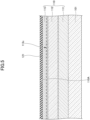
- FIG. 4 through FIG. 9 are cross sectional views illustrating the method for manufacturing the semiconductor device according to the first embodiment.
- the nitride semiconductor layer 110 is formed on the substrate 101 by metal organic chemical vapor deposition (MOCVD), for example.
- MOCVD metal organic chemical vapor deposition
- the buffer layer 111, the barrier layer 112, and the channel layer 113 are formed in this order.
- the strain is generated between the channel layer 113 and the barrier layer 112 due to the difference in the lattice constants thereof, and this strain induces the piezoelectric charge at the interface between the two layers.
- the 2DEG is formed in the region of the channel layer 113 closer to the barrier layer 112, thereby forming the channel region 113c.
- the insulating layer 121 in contact with the front surface 110A of the nitride semiconductor layer 110, is formed.
- the insulating layer 121 can be formed by low pressure CVD (LPCVD), for example.
- LPCVD low pressure CVD
- the insulating layer 121 may be formed continuously on the buffer layer 111, the barrier layer 112, and the channel layer 113 by MOCVD, for example, without exposing the front surface of the channel layer 113 to atmosphere.
- the openings 121S and 121D are formed in the insulating layer 121.
- the openings 121S and 121D can be formed by reactive ion etching (RIE) using a resist pattern (not illustrated) as a mask, for example.
- RIE reactive ion etching
- the RIE uses a fluorine-based gas as a reactive gas, for example.
- the n-type GaN layer 131S is formed on the nitride semiconductor layer 110 inside the opening 121S, and the n-type GaN layer 131D is formed on the nitride semiconductor layer 110 inside the opening 121D.
- Upper surfaces of the n-type GaN layers 131S and 131D may coincide with an upper surface of the insulating layer 121, or may not coincide with the upper surface of the insulating layer 121.
- the n-type GaN layers 131S and 131D can be formed by physical vapor deposition (PVD), such as vapor deposition, sputtering, molecular beam epitaxy (MBE), or the like, for example.
- PVD physical vapor deposition
- MBE molecular beam epitaxy
- a film deposition is performed using a growth mask (not illustrated) having openings formed in regions where the n-type GaN layers 131S and 131D are to be formed, and the growth mask is thereafter removed together with an n-type GaN layer (not illustrated) formed thereon, for example. That is, a lift-off is performed. Details of the method of forming the n-type GaN layers 131S and 131D will be described later.
- the source electrode 132S is formed on the n-type GaN layer 131S
- drain electrode 132D is formed on the n-type GaN layer 131D.
- a metal layer (not illustrated) constituting the source electrode 132S and the drain electrode 132D is formed first.
- a film deposition is performed using a growth mask (not illustrated) having openings formed in regions where the metal layer is to be formed, and the growth mask is thereafter removed together with the metal layer (not illustrated) formed thereon, for example. That is, a lift-off is performed.
- the gate electrode 141 is formed on the insulating layer 121 between the source electrode 132S and the drain electrode 132D.
- a metal layer is formed using a growth mask (not illustrated) having an opening formed in a region where the gate electrode 141 is to be formed, and the growth mask is thereafter removed together with the metal layer (not illustrated) formed thereon, for example. That is, a lift-off is performed.
- the insulating layer 142 is formed on the insulating layer 121 by plasma CVD, for example, so as to cover the gate electrode 141 with the insulating layer 142.
- the semiconductor device 100 can be manufactured in the manner described above.
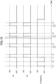
- FIG. 10 is a timing chart illustrating the method of forming the n-type GaN layers 131S and 131D.
- FIG. 10 illustrates whether Ga, Ge, and N radicals are supplied to the nitride semiconductor layer 110 when forming the n-type GaN layers 131S and 131D.
- "ON" indicates that there is a supply
- "OFF” indicates that there is no supply.
- FIG. 11 through FIG. 15 are cross sectional views illustrating the method of forming the n-type GaN layers 131S and 131D.
- a temperature inside the deposition chamber is set to a predetermined temperature and a pressure inside the deposition chamber is set to a predetermined pressure.
- the predetermined temperature and the predetermined pressure are selected so that a saturation vapor pressure of Ga is lower than the predetermined pressure at the predetermined temperature.
- the predetermined temperature is 600°C
- the predetermined pressure is higher than the saturation vapor pressure of Ga at 600°C.
- a saturation vapor pressure of Ge is lower than the saturation vapor pressure of Ga.
- the supply of the N radicals 152 to the nitride semiconductor layer 110 is started at a time t11, and the supply of the N radicals 152 is stopped at a time t12.
- the front surface of the nitride semiconductor layer 110 is cleaned by the supply of the N radicals 152 from the time t11 to the time t12.
- the N radicals 152 are generated by inductively coupled plasma (ICP).
- the supply of Ga, Ge, and the N radicals 152 to the nitride semiconductor layer 110 is started, and at a subsequent time t2, the supply of Ga and Ge is stopped while continuing the supply of the N radicals 152.
- the n-type GaN layer 150 is formed by the supply of Ga, Ge, and the N radicals 152 from time t1 to time t2.
- droplets 151 of an alloy of Ga and Ge are formed on the front surface of the n-type GaN layer 150.
- Ga is supplied by radio frequency (RF) sputtering
- Ge is supplied by direct current (DC) pulse sputtering.
- a time period from the time t1 to the time t2 is 10 seconds or longer and 30 seconds or shorter, and preferably 20 seconds or longer and 30 seconds or shorter, for example.
- a number density of the droplets 151 is approximately 6.1 ⁇ 10 4 cm -2
- an average diameter of the droplets 151 is approximately 300 nm
- a height of the droplets 151 is approximately 57 nm.
- the supply of Ga and Ge is started while continuing the supply of the N radicals 152, similar to the time t1.
- the n-type GaN layer 160 When forming the n-type GaN layer 160, a portion of Ga evaporates as the gas Ga 153 while Ge remains in the droplet 151, and a ratio of Ge with respect to a total amount of Ga and Ge in the droplet 151 becomes higher than a ratio of Ge with respect to a total amount of Ga and Ge in the n-type GaN layer 150. Accordingly, the n-type GaN layer 160 formed of the droplets 151 from which Ga evaporated includes a higher concentration of Ge than the n-type GaN layer 150.
- the time period from the time t2 to the time t3 is 15 seconds or longer and 120 seconds or shorter, for example.
- the supply of Ga and Ge is stopped while continuing the supply of the N radicals.
- an n-type GaN layer 150 is newly formed, and droplets 151 of the alloy of Ga and Ge are formed on the front surface of the n-type GaN layer 150.
- the processes from the time t1 to the time t3 are repeatedly performed.
- the n-type GaN layers 131S and 131D in which the n-type GaN layers 150 and 160 are alternately laminated are formed.
- Each of the n-type GaN layers 150 and 160 may make direct contact with the nitride semiconductor layer 110, for example.
- the Ge precipitation is likely to remain on the front surface of the GaN layer.
- residual Ge precipitation can be suppressed, and a deterioration of electrical characteristics caused by the precipitation can be reduced.
- the surface of the nitride semiconductor layer 110 in contact with lower surfaces of the n-type GaN layers 131S and 131D are N polar surfaces, and the channel layer 113 is located above the barrier layer 112. For this reason, distances between the channel region 113c and the source and drain electrodes 132S and 132D can easily be reduced, and the resistance can easily be reduced.
- the n-type GaN layers 131S and 131D are formed inside the openings 121S and 121D formed in the insulating layer 121, respectively, it is easy to achieve the low resistance while protecting the nitride semiconductor layer 110 by the insulating layer 121.
- the period of the n-type GaN layers 150 and 160 in the thickness direction is preferably 8 nm or less, more preferably 6 nm or less, and still more preferably 4 nm or less.
- the n-type GaN layers 131S and 131D are more likely to have a good crystallinity.
- large droplets 151 are formed when forming the n-type GaN layer 150.
- the n-type GaN layer 160 is formed through migration of Ga atoms in the droplets 151 on the front surface of the n-type GaN layer 150, but in the case where the large droplets 151 are formed, nitridation of Ga may occur at a stage where the migration of the Ga atoms does not sufficiently occur. In this case, it may be difficult to obtain a good n-type GaN layer 160.
- the difference between the first concentration and the second concentration is preferably 1 ⁇ 10 20 cm -3 or higher and 7 ⁇ 10 20 cm -3 or lower, more preferably 2 ⁇ 10 20 cm -3 or higher and 6 ⁇ 10 20 cm -3 or lower, and still more preferably 3 ⁇ 10 20 cm -3 or higher and 5 ⁇ 10 20 cm -3 or lower. If the concentration difference is too small or too large, it may be difficult to obtain the n-type GaN layers 131S and 131D with a good crystallinity.
- the n-type impurity is not particularly limited, but when Ge or Si is used, a low electrical resistance can easily be obtained in the n-type GaN layers 150 and 160.
- the concentration of the impurity, such as Ge, Si, or the like, included in the n-type GaN layers 131S and 131D can be measured by secondary ion mass spectrometry (SIMS).
- SIMS secondary ion mass spectrometry
- the impurity concentration varies in a rectangular wave shape in FIG. 3
- a measurement result of the impurity concentration may vary in a sinusoidal wave shape as illustrated in FIG. 16 .
- ranges of the n-type GaN layers 150 and 160 can be specified by approximating an impurity concentration profile by the rectangular wave shape.
- the droplets 151 formed on the front surface of the n-type GaN layer 150 are preferably eliminated by evaporation, nitridation, or the like. This is because, if the droplets 151 remain, the crystallinity of the n-type GaN layer 160 may deteriorate. A portion of Ga in the droplet 151 may be incorporated into the n-type GaN layer 150.
- the time period from the time t2 to the time t3 is preferably longer than the time period from the time t1 to the time t2. That is, the time in which the n-type GaN layer 150 is formed is preferably longer than the time in which the n-type GaN layer 160 is formed by thereafter continuing the supply of the N radicals 152. This is because the droplets 151 can easily be eliminated.
- a temperature of the substrate 101 when forming the n-type GaN layers 150 and 160 is preferably 200°C or higher and 650°C or lower, more preferably 250°C or higher and 600°C or lower, and still more preferably 300°C or higher and 550°C or lower. This is because, if the temperature of the substrate 101 is too low, it becomes difficult to form the n-type GaN layers 150 and 160, and if the temperature is too high, the nitride semiconductor layer 110 or the like which are already formed may become damaged.
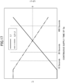
- FIG. 17 is a diagram illustrating a relationship between the continuous supply time of Ga and a droplet size L1.
- FIG. 17 also illustrates a relationship between the continuous supply time of Ga and a difference (L2 - L1) between a migration length L2 and the droplet size L1 (L2 - L1).
- the abscissa represents the continuous supply time of Ga
- the left ordinate represents L1
- the right ordinate represents L2 - L1.
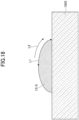
- FIG. 18 and FIG. 19 are cross sectional views illustrating a phenomenon in a case where the continuous supply time of Ga is too long.
- the n-type GaN layer 160 is formed through migration of the Ga atoms in the droplets 151.
- the migration length L2 is approximately 1 ⁇ m or greater and approximately 3 ⁇ m or less, although dependent on conditions, such as the temperature, the pressure, or the like during the time period from the time t2 to the time t1.
- the migration length L2 is defined as a moving distance of the Ga atom from a start of movement to deactivation.
- the droplet size L1 is defined as a length of a shortest path from a top of the surface of the droplet to the front surface of the n-type GaN layer when the droplet is approximated by an ellipsoid.
- a thick n-type GaN layer 150X is formed instead of the n-type GaN layer 150, and a large droplet 151X of the alloy of Ga and Ge is formed on the front surface of the n-type GaN layer 150X, as illustrated in FIG. 18 .
- the droplet size L1 may become larger than the migration length L2 (L2 - L1 ⁇ 0).
- nitridation occurs before the Ga atoms in the droplet 151X spread on the front surface of the n-type GaN layer 150X, and as illustrated in FIG.
- the surface of the droplet 151X is covered with an n-type GaN layer 160X before the droplet 151X disappears.
- the surface of the droplet 151X is covered with the n-type GaN layer 160X, it is difficult to obtain a good flatness. For example, when the time period from the time t1 to the time t2 is approximately 600 seconds, the droplet size L1 becomes approximately 3.5 ⁇ m, and the surface of the droplet 151X may become covered with the n-type GaN layer 160X.
- the droplet size L1 becomes approximately 0.15 ⁇ m
- the droplet size L1 becomes smaller than the migration length L2 (L2 - L1 > 0), and a good n-type GaN layer 160 can be formed.
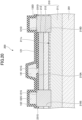
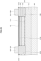
- FIG. 20 is a cross sectional view illustrating the semiconductor device according to the second embodiment.
- a semiconductor device 200 mainly includes a substrate 201, a nitride semiconductor layer 210, an insulating layer 121, an n-type GaN layer 231S, an n-type GaN layer 231D, a gate electrode 141, a source electrode 132S, a drain electrode 132D, and an insulating layer 142.
- the substrate 201 is a substrate for growing a GaN-based semiconductor, for example, and is a semiinsulating SiC substrate, for example.
- a front surface of the substrate 201 is a silicon (Si) polar surface.
- the nitride semiconductor layer 210 can undergo crystal growth using a Ga polar surface as a growth surface.
- the nitride semiconductor layer 210 includes a channel layer 211, a barrier layer 212, and a cap layer 213.
- the nitride semiconductor layer 210 is an example of the first nitride semiconductor layer.
- the channel layer 211 is a GaN layer, for example.
- a thickness of the channel layer 211 is in a range of 200 nm or greater and 2000 nm or less, for example, and is 1000 nm in one embodiment.
- a buffer layer may be provided between the channel layer 211 and the substrate 201.
- the barrier layer 212 is an AlGaN layer, for example.
- a band gap of the barrier layer 212 is larger than a band gap of the channel layer 211.
- a thickness of the barrier layer 212 is in a range of 5 nm or greater and 30 nm or less, for example, and is 15 nm in one embodiment.
- an Al composition x thereof is 0.15 or greater and 0.35 or less, for example, and is 0.25 in one embodiment.
- a strain is generated between the channel layer 211 and the barrier layer 212 due to a difference in lattice constants thereof, and this strain induces a piezoelectric charge at an interface between the two layers.
- a 2DEG is generated in a region of the channel layer 211 closer to the barrier layer 212, thereby forming a channel region 211c.
- An InAlN layer or an InAlGaN layer may be used in place of the AlGaN layer.
- a spacer layer may be provided between the channel layer 211 and the barrier layer 212.
- the spacer layer is an AlN layer, for example.
- a thickness of the spacer layer is in a range of 0.5 nm or greater and 3.0 nm or less, for example, and is 1.0 nm in one embodiment.
- the cap layer 213 is a GaN layer, for example.
- a thickness of the cap layer 213 is in a range of 0 nm or greater and 5 nm or less, for example, and is 2 nm in one embodiment.
- a front surface of the cap layer 213 constitutes a front surface 210A of the nitride semiconductor layer 210.
- the channel layer 211, the barrier layer 212, and the cap layer 213 undergo crystal growth using the Ga polar surface as the growth surface. Accordingly, front surfaces of the channel layer 211, the barrier layer 212, and the cap layer 213 opposite to back surfaces thereof facing the substrate 201 become Ga polar surfaces, and the back surfaces thereof facing the substrate 201 become N polar surfaces.
- Recesses 210S and 210D are formed in the nitride semiconductor layer 210.
- the recesses 210S and 210D are formed to a depth penetrating the channel region 211c. That is, depths of the recesses 210S and 210D are greater than a depth of the channel region 211c with reference to the front surface 210A of the nitride semiconductor layer 210. Bottom surfaces of the recesses 210S and 210D may be located inside the barrier layer 212.
- the insulating layer 121 is in contact with the front surface 210A of the nitride semiconductor layer 210. Openings 121S and 121D are formed in the insulating layer 121. The opening 121S connects to the recess 210S, and the opening 121D connects to the recess 210D.
- the n-type GaN layer 231S is formed on the nitride semiconductor layer 210 inside the recess 210S and the opening 121S.
- the n-type GaN layer 231D is formed on the nitride semiconductor layer 210 inside the recess 210D and the opening 121D.
- the n-type GaN layers 231S and 231D include Ge or Si as the n-type impurity.
- the n-type GaN layers 231S and 231D are examples of the second nitride semiconductor layer.
- FIG. 21 is a cross sectional view illustrating the n-type GaN layers 231S and 231D in the second embodiment.
- the n-type GaN layers 231S and 231D include a plurality of n-type GaN layers 250 and a plurality of n-type GaN layers 260.
- the n-type GaN layers 250 and 260 are alternately laminated on the nitride semiconductor layer 210.
- the n-type GaN layers 250 and 260 are laminated on the nitride semiconductor layer 210 with a period of 8 nm or less.
- the n-type GaN layer 250 includes an n-type impurity with a first concentration of 1 ⁇ 10 20 cm -3 or higher.
- the n-type GaN layer 250 includes the n-type impurity with the first concentration of 3 ⁇ 10 20 cm -3
- the n-type GaN layer 260 includes an n-type impurity with a second concentration higher than the first concentration, such as 9 ⁇ 10 20 cm -3 , for example.
- a difference between the first concentration and the second concentration is 6 ⁇ 10 20 cm -3 .
- the impurity concentration periodically varies in the depth direction.
- the n-type GaN layer 250 is an example of the third nitride semiconductor layer
- the n-type GaN layer 260 is an example of the fourth nitride semiconductor layer.
- the source electrode 132S is formed on the n-type GaN layer 231S
- the drain electrode 132D is formed on the n-type GaN layer 231D.
- An opening 121G is formed in the insulating layer 121 between the source electrode 132S and the drain electrode 132D. A portion of the nitride semiconductor layer 210 is exposed via the opening 121G.
- the gate electrode 141 is formed on the insulating layer 121 so as to make contact with the nitride semiconductors 210 via the opening 121G.
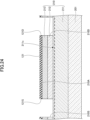
- FIG. 22 through FIG. 27 are cross sectional views illustrating the method for manufacturing the semiconductor device according to the second embodiment.
- the nitride semiconductor layer 210 is formed on the substrate 201 by MOCVD, for example.
- MOCVD MOCVD
- the channel layer 211, the barrier layer 212, and the cap layer 213 are formed in this order.
- a strain is generated between the channel layer 211 and the barrier layer 212 due to the difference in lattice constant thereof, and this strain induces a piezoelectric charge at the interface between the two layers.
- a 2DEG is formed in a region of the channel layer 211 closer to the barrier layer 212, thereby forming the channel region 211c.
- the insulating layer 121 in contact with the front surface 210A of the nitride semiconductor layer 210, is formed.
- the insulating layer 121 can be formed by low pressure CVD, for example.
- the insulating layer 121 may be formed continuously on the channel layer 211, the barrier layer 212, and the cap layer 213 by MOCVD, for example, without exposing the front surface of the cap layer 213 to the atmosphere.
- the openings 121S and 121D are formed in the insulating layer 121, and the recesses 210S and 210D are formed in the nitride semiconductor layer 210.
- the openings 121S and 121D and the recesses 210S and 210D can be formed by RIE using resist patterns (not illustrated) as masks, for example.
- a fluorine-based gas is used as a reactive gas in the RIE of the insulating layer 121
- a chlorine-based gas is used as a reactive gas in the RIE of the nitride semiconductor layer 210.
- the n-type GaN layer 231S is formed on the nitride semiconductor layer 210 inside the opening 121S and the recess 210S, and the n-type GaN layer 231D is formed on the nitride semiconductor layer 210 inside the opening 121D and the recess 210D.
- the upper surfaces of the n-type GaN layers 231S and 231D may coincide with the upper surface of the insulating layer 121, or may not coincide with the upper surface of the insulating layer 121.
- the n-type GaN layers 231S and 231D can be formed by the same method as that used to form the n-type GaN layers 131S and 131D.
- Each of the n-type GaN layers 250 and 260 may make direct contact with the nitride semiconductor layer 110, for example.
- the density and size of the droplets in the present embodiment are different from those of the first embodiment because the growth surface in the present embodiment is different from that in the first embodiment.
- the number density of the droplets is approximately 1.0 ⁇ 10 7 cm -2
- the average diameter of the droplets is approximately 60 nm or greater and 100 nm or less
- the height of the droplets is approximately 20 nm.
- the source electrode 132S is formed on the n-type GaN layer 131S, and the drain electrode 132D is formed on the n-type GaN layer 131D.
- the source electrode 132S and the drain electrode 132D can be formed by the same method as that used in the first embodiment.
- the opening 121G is formed in the insulating layer 121 between the source electrode 132S and the drain electrode 132D. A portion of the nitride semiconductor layer 210 is exposed via the opening 121G.
- the gate electrode 141 in contact with the nitride semiconductor layer 210 via the opening 121G, is formed.
- the gate electrode 141 can be formed by the same method as that used in the first embodiment.
- the semiconductor device 200 can be manufactured in the manner described above.
- the n-type GaN layer 250 includes the n-type impurity such as Ge or the like with the first concentration of 1 ⁇ 10 20 cm -3 or higher, and the n-type GaN layer 260 includes the n-type impurity such as Ge or the like with the second concentration higher than the first concentration. Accordingly, the electrical resistance of the n-type GaN layers 231S and 231D can be sufficiently reduced.
- the n-type GaN layers 250 and 260 having the different concentrations of the n-type impurity are alternately laminated, a good crystallinity can be obtained although the n-type impurity concentration is high.
- the n-type GaN layers 250 and 260 can be formed by PVD at a temperature at which a damage to the nitride semiconductor layer 210 formed before the formation of these two layers is suppressed. That is, the n-type GaN layers 250 and 260 having a good crystallinity can be formed using an existing film forming apparatus. By lowering the formation temperature of the n-type GaN layers 250 and 260, the effects of improving the throughput and reducing the greenhouse gas emissions can also be obtained.
- the surface of the nitride semiconductor layer 210 in contact with the lower surfaces of the n-type GaN layers 231S and 231D are Ga polar surfaces, and the barrier layer 212 is located above the channel layer 211. For this reason, the nitride semiconductor layer 210 can easily be grown, and the upper surface of the nitride semiconductor layer 210 can easily exhibit a good etching resistance.
- the n-type GaN layers 231S and 231D are formed inside the recesses 210S and 210D formed in the nitride semiconductor layer 210, respectively, the distances between the channel region 211c and the n-type GaN layers 231S and 231D can easily be reduced, and the resistance can easily be reduced.
Landscapes
- Junction Field-Effect Transistors (AREA)
- Thyristors (AREA)
Abstract
Description
- The present disclosure relates to semiconductor devices and methods for manufacturing semiconductor devices.
- The present application is based upon and claims priority to
Japanese Patent Application No. 2022-096882, filed on June 15, 2022 - A structure in which a nitride semiconductor layer including a high concentration of an impurity is regrown has been proposed, in order to reduce a contact resistance or the like in a semiconductor device using a nitride semiconductor.
-
- Patent Document 1:
Japanese Laid-Open Patent Publication No. 2008-270749 - Patent Document 2:
Japanese Laid-Open Patent Publication No. 2019-041113 - Patent Document 3:
Japanese Laid-Open Patent Publication No. 2017-059671 - NON-PATENT DOCUMENT 1: Applied Physics Express, 2 (2009) 051001
- A semiconductor device according to the present disclosure includes a first nitride semiconductor layer including gallium, and a second nitride semiconductor layer formed on the first nitride semiconductor layer and including gallium, wherein the second nitride semiconductor layer includes a plurality of third nitride semiconductor layers and a plurality of fourth nitride semiconductor layers alternately laminated on the first nitride semiconductor layer, the plurality of third nitride semiconductor layers include an impurity of a first conductivity type with a first concentration, the plurality of fourth nitride semiconductor layers include the impurity of the first conductivity type with a second concentration higher than the first concentration, and the first concentration is 1 × 1020 cm-3 or higher.
-
- [
FIG. 1] FIG. 1 is a cross sectional view illustrating a semiconductor device according to a first embodiment. - [
FIG. 2] FIG. 2 is a cross sectional view illustrating an n-type GaN layer in the first embodiment. - [
FIG. 3] FIG. 3 is a diagram illustrating a relationship between a depth from front surfaces of n-type GaN layers and an impurity concentration in the first embodiment. - [
FIG. 4] FIG. 4 is a cross sectional view (Part 1) illustrating a method for manufacturing the semiconductor device according to the first embodiment. - [
FIG. 5] FIG. 5 is a cross sectional view (Part 2) illustrating the method for manufacturing the semiconductor device according to the first embodiment. - [
FIG. 6] FIG. 6 is a cross sectional view (Part 3) illustrating the method for manufacturing the semiconductor device according to the first embodiment. - [
FIG. 7] FIG. 7 is a cross sectional view (Part 4) illustrating the method for manufacturing the semiconductor device according to the first embodiment. - [
FIG. 8] FIG. 8 is a cross sectional view (Part 5) illustrating the method for manufacturing the semiconductor device according to the first embodiment. - [
FIG. 9] FIG. 9 is a sectional view (Part 6) illustrating the method for manufacturing the semiconductor device according to the first embodiment. - [
FIG. 10] FIG. 10 is a timing chart illustrating a method of forming n-type GaN layers in the first embodiment. - [
FIG. 11] FIG. 11 is a cross sectional view (Part 1) illustrating a method of forming the n-type GaN layers according to the first embodiment. - [
FIG. 12] FIG. 12 is a cross sectional view (Part 2) illustrating the method of forming the n-type GaN layers according to the first embodiment. - [
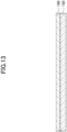
FIG. 13] FIG. 13 is a cross sectional view (Part 3) illustrating the method of forming the n-type GaN layers according to the first embodiment. - [
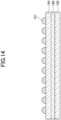
FIG. 14] FIG. 14 is a cross sectional view (Part 4) illustrating the method of forming the n-type GaN layers according to the first embodiment. - [
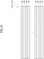
FIG. 15] FIG. 15 is a cross sectional view (Part 5) illustrating the method of forming the n-type GaN layers according to the first embodiment. - [
FIG. 16] FIG. 16 is a diagram illustrating another example of the relationship between the depth from the front surfaces of the n-type GaN layers and the impurity concentration in the first embodiment. - [
FIG. 17] FIG. 17 is a diagram illustrating a relationship between a continuous supply time of Ga, a droplet size L1, and a difference between a migration length L2 and the droplet size L1. - [
FIG. 18] FIG. 18 is a cross sectional view (Part 1) illustrating a phenomenon in a case where the continuous supply time of Ga is too long. - [
FIG. 19] FIG. 19 is a cross sectional view (Part 2) illustrating the phenomenon in the case where the continuous supply time of Ga is too long. - [
FIG. 20] FIG. 20 is a cross sectional view illustrating the semiconductor device according to a second embodiment. - [
FIG. 21] FIG. 21 is a cross sectional view illustrating the n-type GaN layers in the second embodiment. - [
FIG. 22] FIG. 22 is a cross sectional view (Part 1) illustrating the method for manufacturing the semiconductor device according to the second embodiment. - [
FIG. 23] FIG. 23 is a cross sectional view (Part 2) illustrating the method for manufacturing the semiconductor device according to the second embodiment. - [
FIG. 24] FIG. 24 is a cross sectional view (Part 3) illustrating the method for manufacturing the semiconductor device according to the second embodiment. - [
FIG. 25] FIG. 25 is a cross sectional view (Part) illustrating the method for manufacturing the semiconductor device according to the second embodiment. - [
FIG. 26] FIG. 26 is a cross sectional view (Part 4) illustrating the method for manufacturing the semiconductor device according to the second embodiment. - [
FIG. 27] FIG. 27 is a cross sectional view (Part 5) illustrating the method for manufacturing the semiconductor device according to the second embodiment. - In conventional semiconductor devices, electrical characteristics may deteriorate due to precipitation of an impurity element.
- One object of the present disclosure is to provide a semiconductor device and a method for manufacturing the semiconductor device, which can reduce deterioration of the electrical characteristics caused by the precipitation of the impurity element.
- According to the present disclosure, it is possible to reduce the deterioration of the electrical characteristics caused by the precipitation of the impurity element.
- First, embodiments of the present disclosure will be listed and described.
- [1] A semiconductor device according to one aspect of the present disclosure includes a first nitride semiconductor layer including gallium; and a second nitride semiconductor layer formed on the first nitride semiconductor layer and including gallium, wherein the second nitride semiconductor layer includes a plurality of third nitride semiconductor layers and a plurality of fourth nitride semiconductor layers alternately laminated on the first nitride semiconductor layer, the plurality of third nitride semiconductor layers include an impurity of a first conductivity type with a first concentration, the plurality of fourth nitride semiconductor layers include the impurity of the first conductivity type with a second concentration higher than the first concentration, and the first concentration is 1 × 1020 cm-3 or higher.
The third nitride semiconductor layer includes the impurity of the first conductivity type with the first concentration of 1 × 1020 cm-3 or higher, and the fourth nitride semiconductor layer includes the impurity of the first conductivity type with the second concentration higher than the first concentration. Accordingly, the deterioration of the electrical characteristics caused by precipitation of the impurity element can be reduced. In addition, because the third nitride semiconductor layer and the fourth nitride semiconductor layer having the different impurity concentrations are alternately laminated, a good crystallinity can be obtained although the impurity concentration is high. Further, the third nitride semiconductor layer and the fourth nitride semiconductor layer can be formed by physical vapor deposition, for example. That is, the third nitride semiconductor layer and the fourth nitride semiconductor layer having the good crystallinity can be formed using an existing film forming apparatus. - [2] In [1] above, the plurality of third nitride semiconductor layers and the plurality of fourth nitride semiconductor layers may be laminated with a period of 8 nm or less. As this period becomes smaller, it becomes more likely that the second nitride semiconductor layer having the good crystallinity can be obtained.
- [3] In [1] or [2] above, a difference between the first concentration and the second concentration may be 1 × 1020 cm-3 or higher and 7 × 1020 cm-3 or lower. If the concentration difference is too small or too large, it may be difficult to obtain the second nitride semiconductor layer with a good crystallinity.
- [4] In any of [1] to [3] above, the impurity may be germanium or silicon. When the impurity is germanium or silicon, a low electrical resistance can easily be obtained in the second nitride semiconductor layer.
- [5] In any one of [1] to [4] above, an ohmic electrode may be formed on the second nitride semiconductor layer. In this case, a low electrical resistance can be obtained between the first nitride semiconductor layer and the ohmic electrode.
- [6] In any one of [1] to [5] above, a surface of the first nitride semiconductor layer in contact with a lower surface of the second nitride semiconductor layer may be a nitrogen polar surface. In this case, a low resistance can easily be obtained.
- [7] In [6] above, the first nitride semiconductor layer may include a barrier layer, and a channel layer provided above the barrier layer. In this case, a low resistance can easily be obtained.
- [8] In [6] or [7] above, an insulating layer may be formed on the first nitride semiconductor layer, the insulating layer may include an opening exposing the first nitride semiconductor layer, and the second nitride semiconductor layer may be formed inside the opening. In this case, it is easy to reduce the resistance while protecting the first nitride semiconductor layer with the insulating layer.
- [9] In any one of [1] to [5] above, a surface of the first nitride semiconductor layer in contact with a lower surface of the second nitride semiconductor layer may be a gallium polar surface. In this case, it is easy to grow the first nitride semiconductor layer, and an upper surface of the first nitride semiconductor layer can easily exhibit a good etching resistance.
- [10] In [9] above, the first nitride semiconductor layer may include a channel layer, and a barrier layer provided above the channel layer. In this case, it is easy to grow the first nitride semiconductor layer, and the upper surface of the first nitride semiconductor layer can easily exhibit a good etching resistance.
- [11] In [9] or [10] above, the first nitride semiconductor layer may be formed with a recess, and the second nitride semiconductor layer may be formed inside the recess. In this case, a low resistance can easily be obtained.
- [12] A method for manufacturing a semiconductor device according to another aspect of the present disclosure includes the steps of forming, on a first nitride semiconductor layer including gallium, a second nitride semiconductor layer including gallium by physical vapor deposition, wherein the step of forming the second nitride semiconductor layer includes repeating the steps of forming a third nitride semiconductor layer including an impurity of a first conductivity type with a first concentration, and forming droplets of an alloy of gallium and the impurity on a surface of the third nitride semiconductor layer, and forming a fourth nitride semiconductor layer including the impurity of the first conductivity type with a second concentration higher than the first concentration, by evaporating a portion of the gallium from the droplets and nitriding another portion of the gallium in the droplets while incorporating the impurity in the droplet.
When forming the second nitride semiconductor layer by the physical vapor deposition, the forming of the third nitride semiconductor layer and the forming of the fourth nitride semiconductor layer are repeated. When forming the third nitride semiconductor layer, the droplets of the alloy of gallium and the impurity are formed on the surface of the third nitride semiconductor layer, and when forming the fourth nitride semiconductor layer, a portion of the gallium is evaporated from the droplets, and the other portion of the gallium in the droplets is nitrided while incorporating the impurity in the droplets. Accordingly, even in a case where the third nitride semiconductor layer includes the impurity of the first conductivity type with a high concentration of 1 × 1020 cm-3 or higher for example, the third nitride semiconductor layer and the fourth nitride semiconductor layer can have a good crystallinity. For this reason, residual impurity precipitation can be suppressed at the surface of the second nitride semiconductor layer, and a deterioration of electrical characteristics caused by the precipitation can be reduced. - [13] In [12] above, the step of forming the fourth nitride semiconductor layer may eliminate the droplets. If the droplets remain, the crystallinity of the fourth nitride semiconductor layer may deteriorate.
- [14] In [12] or [13] above, a duration of the step of forming the fourth nitride semiconductor layer is longer than a duration of the step of forming the third nitride semiconductor layer. In this case, the droplets can easily be eliminated.
- [15] In any one of [12] to [14] above, the third nitride semiconductor layer and the fourth nitride semiconductor layer may be formed inside a chamber, and in the steps of forming of the third nitride semiconductor layer and forming of the fourth nitride semiconductor layer, a saturation vapor pressure of gallium may be lower than a pressure inside the chamber at a temperature inside the chamber. In this case, the droplets including the gallium are likely formed stably.
- [16] In any one of [12] to [15] above, the first nitride semiconductor layer may be formed on a substrate, and a temperature of the substrate when forming the third nitride semiconductor layer and the fourth nitride semiconductor layer may be 200°C or higher and 650°C or lower. If the temperature of the substrate is too low, it is difficult to form the third nitride semiconductor layer and the fourth nitride semiconductor layer, and if the temperature of the substrate is too high, the first nitride semiconductor layer or the like which is already formed may become damaged.
- Hereinafter, embodiments of the present disclosure will be described in detail, but the present disclosure is not limited these embodiments. In the specification and the drawings, constituent elements having substantially the same functional configuration are designated by the same reference numerals, and a redundant description thereof may be omitted.
- First, a first embodiment will be described. The first embodiment relates to a semiconductor device including a GaN-based high electron mobility transistor (HEMT).
FIG. 1 is a cross sectional view illustrating the semiconductor device according to the first embodiment. - As illustrated in
FIG. 1 , asemiconductor device 100 according to the first embodiment mainly includes asubstrate 101, anitride semiconductor layer 110, an insulatinglayer 121, an n-type gallium nitride (GaN)layer 131S, an n-type GaN layer 131D, agate electrode 141, asource electrode 132S, adrain electrode 132D, and an insulatinglayer 142. - The
substrate 101 is a substrate for growing a GaN-based semiconductor, for example, and is a semiinsulating silicon carbide (SiC) substrate, for example. In a case where thesubstrate 101 is the SiC substrate, a front surface of thesubstrate 101 is a carbon (C) polar surface. In the case where the front surface of thesubstrate 101 is the C polar surface, thenitride semiconductor layer 110 can undergo crystal growth using a nitrogen (N) polar surface as a growth surface. A sapphire substrate may be used as the substrate for growing the GaN-based semiconductor. Thesubstrate 101 does not have to be the substrate for crystal growth, and in this case, thenitride semiconductor layer 110 may be grown on another substrate, and after removing this other substrate from thenitride semiconductor layer 110, thesubstrate 101 may be bonded to thenitride semiconductor layer 110. In this case, a semiinsulating substrate made of various materials, such as a sapphire substrate, a silicon (Si) substrate, a SiC substrate, an aluminum nitride (AlN) substrate, a sintered body, or the like, for example, may be used as thesubstrate 101. - The
nitride semiconductor layer 110 includes abuffer layer 111, abarrier layer 112, and achannel layer 113. Thenitride semiconductor layer 110 is an example of a first nitride semiconductor layer. - The
buffer layer 111 is an AlN layer, for example. A thickness of the AlN layer is 5 nm or greater and 100 nm or less, for example. Thebuffer layer 111 may include an AlN layer, and a GaN layer or an aluminum gallium nitride (AlGaN) layer on the AlN layer. A thickness of the GaN layer or the AlGaN layer is 300 nm or greater and 2000 nm or less, for example. - The
barrier layer 112 is an AlGaN layer, for example. A band gap of thebarrier layer 112 is larger than a band gap of thechannel layer 113 which will be described later. A thickness of thebarrier layer 112 is in a range of 5 nm or greater and 50 nm or less, for example, and is 30 nm in one embodiment. In a case where thebarrier layer 112 is a AlxGa1-xN layer, an Al composition x thereof is 0.15 or greater and 0.55 or less, for example, and is 0.35 in one embodiment. A conductivity type of thebarrier layer 112 is an n-type or undoped (i-type), for example. An indium aluminum nitride (InAlN) layer or an indium aluminum gallium nitride (InAlGaN) layer may be used in place of the AlGaN layer. - The
channel layer 113 is a GaN layer, for example. The band gap of thechannel layer 113 is smaller than the band gap of thebarrier layer 112. A thickness of thechannel layer 113 is in a range of 5 nm or greater and 30 nm or less, for example, and is 9 nm in one embodiment. A strain is generated between thechannel layer 113 and thebarrier layer 112 due to a difference in lattice constants thereof, and this strain induces a piezoelectric charge at an interface between the two layers. Hence, a two-dimensional electron gas (2DEG) is generated in a region of thechannel layer 113 closer to thebarrier layer 112, thereby forming achannel region 113c. A conductivity type of thechannel layer 113 is the n-type or undoped (i-type), for example. A front surface of thechannel layer 113 constitutes afront surface 110A of thenitride semiconductor layer 110. A spacer layer may be formed between thebarrier layer 112 and thechannel layer 113. The spacer layer is an AlN layer, for example. A thicknesses of the spacer layer is in a range of 0.5 nm or greater and 3.0 nm or less, for example, and is 1.0 nm in one embodiment. - On the C polar surface of the SiC substrate, the
buffer layer 111, thebarrier layer 112, and thechannel layer 113 undergo crystal growth using the N polar surface as the growth surface. Accordingly, front surfaces of thebuffer layer 111, thebarrier layer 112, and thechannel layer 113 opposite to back surfaces thereof facing thesubstrate 101 become N polar surfaces, and the back surfaces thereof facing thesubstrate 101 become gallium (Ga) polar surfaces. - The insulating
layer 121 makes contact with thefront surface 110A of thenitride semiconductor layer 110. The insulatinglayer 121 is a silicon nitride (SiN) layer, for example.Openings layer 121. A portion of thenitride semiconductor layer 110 is exposed via theopening 121S, and another portion of thenitride semiconductor layer 110 is exposed via theopening 121D. - The n-
type GaN layer 131S is formed on thenitride semiconductor layer 110 inside the opening 121S. The n-type GaN layer 131D is formed on thenitride semiconductor layer 110 inside theopening 121D. The n-type GaN layers 131S and 131D include germanium (Ge) or Si as an n-type impurity. The n-type GaN layers 131S and 131D are examples of a second nitride semiconductor layer. - Next, the n-type GaN layers 131S and 131D will be described in detail.
FIG. 2 is a cross sectional view illustrating the n-type GaN layers 131S and 131D in the first embodiment.FIG. 3 is a diagram illustrating a relationship between a depth from front surfaces of the n-type GaN layers 131S and 131D and an impurity concentration in the first embodiment. - As illustrated in
FIG. 2 , the n-type GaN layers 131S and 131D, which are examples of the second nitride semiconductor layer, include a plurality of n-type GaN layers 150 and a plurality of n-type GaN layers 160. The n-type GaN layers 150 and 160 are alternately laminated on thenitride semiconductor layer 110. For example, the n-type GaN layers 150 and 160 are laminated on thenitride semiconductor layer 110 with a period of 8 nm or less. The n-type GaN layer 150 includes an n-type impurity with a first concentration of 1 × 1020 cm-3 or higher. The n-type GaN layer 150 includes the n-type impurity with the first concentration of 3 × 1020 cm-3, for example, and the n-type GaN layer 160 includes an n-type impurity with a second concentration higher than the first concentration, such as 9 × 1020 cm-3, for example. In this example, a difference between the first concentration and the second concentration is 6 × 1020 cm-3. For this reason, as illustrated inFIG. 3 , in the n-type GaN layers 131S and 131D, the impurity concentration periodically varies in a depth direction. The n-type GaN layers 131S and 131D have the n-type GaN layer 150 as a lowermost layer and the n-type GaN layer 160 as an uppermost layer, for example. The n-type GaN layer 150 is an example of a third nitride semiconductor layer, and the n-type GaN layer 160 is an example of a fourth nitride semiconductor layer. - As illustrated in
FIG. 1 , thesource electrode 132S is formed on the n-type GaN layer 131S, and thedrain electrode 132D is formed on the n-type GaN layer 131D. The source electrode 132S and thedrain electrode 132D include a laminated structure in which a tantalum (Ta) film, an Al film, and a Ta film are laminated in this order, for example. The source electrode 132S and thedrain electrode 132D may include a laminated structure in which a titanium (Ti) film, an Al film, and a Ti film are laminated in this order, or a laminated structure in which a nickel (Ni) film and a gold (Au) film are laminated in this order, for example. The source electrode 132S and thedrain electrode 132D are examples of an ohmic electrode. - The
gate electrode 141 is formed on the insulatinglayer 121 between thesource electrode 132S and thedrain electrode 132D. Thegate electrode 141 includes a laminated structure in which a Ni film, a palladium (Pd) film, and an Au film are laminated in this order, for example. The insulatinglayer 142 is formed on the insulatinglayer 121, and covers thegate electrode 141. - Next, a method for manufacturing the
semiconductor device 100 according to the first embodiment will be described.FIG. 4 through FIG. 9 are cross sectional views illustrating the method for manufacturing the semiconductor device according to the first embodiment. - First, as illustrated in
FIG. 4 , thenitride semiconductor layer 110 is formed on thesubstrate 101 by metal organic chemical vapor deposition (MOCVD), for example. When forming thenitride semiconductor layer 110, thebuffer layer 111, thebarrier layer 112, and thechannel layer 113 are formed in this order. The strain is generated between thechannel layer 113 and thebarrier layer 112 due to the difference in the lattice constants thereof, and this strain induces the piezoelectric charge at the interface between the two layers. Hence, the 2DEG is formed in the region of thechannel layer 113 closer to thebarrier layer 112, thereby forming thechannel region 113c. - Next, as illustrated in
FIG. 5 , the insulatinglayer 121, in contact with thefront surface 110A of thenitride semiconductor layer 110, is formed. The insulatinglayer 121 can be formed by low pressure CVD (LPCVD), for example. The insulatinglayer 121 may be formed continuously on thebuffer layer 111, thebarrier layer 112, and thechannel layer 113 by MOCVD, for example, without exposing the front surface of thechannel layer 113 to atmosphere. - Next, as illustrated in
FIG. 6 , theopenings layer 121. Theopenings - Next, as illustrated in
FIG. 7 , the n-type GaN layer 131S is formed on thenitride semiconductor layer 110 inside the opening 121S, and the n-type GaN layer 131D is formed on thenitride semiconductor layer 110 inside theopening 121D. Upper surfaces of the n-type GaN layers 131S and 131D may coincide with an upper surface of the insulatinglayer 121, or may not coincide with the upper surface of the insulatinglayer 121. The n-type GaN layers 131S and 131D can be formed by physical vapor deposition (PVD), such as vapor deposition, sputtering, molecular beam epitaxy (MBE), or the like, for example. When forming the n-type GaN layers 131S and 131D, a film deposition is performed using a growth mask (not illustrated) having openings formed in regions where the n-type GaN layers 131S and 131D are to be formed, and the growth mask is thereafter removed together with an n-type GaN layer (not illustrated) formed thereon, for example. That is, a lift-off is performed. Details of the method of forming the n-type GaN layers 131S and 131D will be described later. - Next, as illustrated in
FIG. 8 , thesource electrode 132S is formed on the n-type GaN layer 131S, anddrain electrode 132D is formed on the n-type GaN layer 131D. When forming thesource electrode 132S and thedrain electrode 132D, a metal layer (not illustrated) constituting thesource electrode 132S and thedrain electrode 132D is formed first. When forming the metal layer, a film deposition is performed using a growth mask (not illustrated) having openings formed in regions where the metal layer is to be formed, and the growth mask is thereafter removed together with the metal layer (not illustrated) formed thereon, for example. That is, a lift-off is performed. - Next, as illustrated in
FIG. 9 , thegate electrode 141 is formed on the insulatinglayer 121 between thesource electrode 132S and thedrain electrode 132D. When forming thegate electrode 141, a metal layer is formed using a growth mask (not illustrated) having an opening formed in a region where thegate electrode 141 is to be formed, and the growth mask is thereafter removed together with the metal layer (not illustrated) formed thereon, for example. That is, a lift-off is performed. After forming thegate electrode 141, the insulatinglayer 142 is formed on the insulatinglayer 121 by plasma CVD, for example, so as to cover thegate electrode 141 with the insulatinglayer 142. - The
semiconductor device 100 can be manufactured in the manner described above. - Next, a method of forming the n-type GaN layers 131S and 131D will be described. It is assumed in this example that the n-type GaN layers 131S and 131D are formed by sputtering. Further, it is assumed that Ge is used as the n-type impurity.
FIG. 10 is a timing chart illustrating the method of forming the n-type GaN layers 131S and 131D.FIG. 10 illustrates whether Ga, Ge, and N radicals are supplied to thenitride semiconductor layer 110 when forming the n-type GaN layers 131S and 131D. InFIG. 10 , "ON" indicates that there is a supply, and "OFF" indicates that there is no supply.FIG. 11 through FIG. 15 are cross sectional views illustrating the method of forming the n-type GaN layers 131S and 131D. - After the
substrate 101 formed with thenitride semiconductor layer 110 or the like is placed inside a deposition chamber, a temperature inside the deposition chamber is set to a predetermined temperature and a pressure inside the deposition chamber is set to a predetermined pressure. The predetermined temperature and the predetermined pressure are selected so that a saturation vapor pressure of Ga is lower than the predetermined pressure at the predetermined temperature. For example, the predetermined temperature is 600°C, and the predetermined pressure is higher than the saturation vapor pressure of Ga at 600°C. A saturation vapor pressure of Ge is lower than the saturation vapor pressure of Ga. - When the temperature and the pressure inside the chamber stabilize to the predetermined temperature and the predetermined pressure, respectively, the supply of the
N radicals 152 to thenitride semiconductor layer 110 is started at a time t11, and the supply of theN radicals 152 is stopped at a time t12. The front surface of thenitride semiconductor layer 110 is cleaned by the supply of theN radicals 152 from the time t11 to the time t12. For example, theN radicals 152 are generated by inductively coupled plasma (ICP). - At a subsequent time t1, the supply of Ga, Ge, and the
N radicals 152 to thenitride semiconductor layer 110 is started, and at a subsequent time t2, the supply of Ga and Ge is stopped while continuing the supply of theN radicals 152. As illustrated inFIG. 11 , the n-type GaN layer 150 is formed by the supply of Ga, Ge, and theN radicals 152 from time t1 to time t2. Further, simultaneously with the formation of the n-type GaN layer 150,droplets 151 of an alloy of Ga and Ge are formed on the front surface of the n-type GaN layer 150. For example, Ga is supplied by radio frequency (RF) sputtering, and Ge is supplied by direct current (DC) pulse sputtering. A time period from the time t1 to the time t2 is 10 seconds or longer and 30 seconds or shorter, and preferably 20 seconds or longer and 30 seconds or shorter, for example. - For example, a number density of the
droplets 151 is approximately 6.1 × 104 cm-2, an average diameter of thedroplets 151 is approximately 300 nm, and a height of thedroplets 151 is approximately 57 nm. - At a subsequent time t3, the supply of Ga and Ge is started while continuing the supply of the
N radicals 152, similar to the time t1. - Because the supply of Ga is stopped during a time period from the time t2 to the time t3, a portion of Ga evaporates from the
droplet 151 as agas Ga 153, as illustrated inFIG. 12 . On the other hand, although the supply of Ge is also stopped, Ge remains in thedroplet 151 because the saturation vapor pressure of Ge is lower than the saturation vapor pressure of Ga. Further, because the supply of theN radicals 152 continues, Ga in thedroplet 151 incorporates Ge while being nitrided. As a result, as illustrated inFIG. 13 , the n-type GaN layer 160 is formed. When forming the n-type GaN layer 160, a portion of Ga evaporates as thegas Ga 153 while Ge remains in thedroplet 151, and a ratio of Ge with respect to a total amount of Ga and Ge in thedroplet 151 becomes higher than a ratio of Ge with respect to a total amount of Ga and Ge in the n-type GaN layer 150. Accordingly, the n-type GaN layer 160 formed of thedroplets 151 from which Ga evaporated includes a higher concentration of Ge than the n-type GaN layer 150. The time period from the time t2 to the time t3 is 15 seconds or longer and 120 seconds or shorter, for example. - In addition, even if the ratio of Ge in the
droplet 151 increases with the evaporation of Ga, Ge does not agglomerate to such an extent that a critical nucleus is formed. Even if a fine single Ge were temporarily generated, the single Ge would decompose before growing to the critical nucleus, because the supply of Ge is also stopped during the time period from the time t2 to the time t3. For this reason, no Ge precipitation is generated also when forming the n-type GaN layer 160. - At the subsequent time t2, the supply of Ga and Ge is stopped while continuing the supply of the N radicals. As illustrated in
FIG. 14 , by the supply of Ga, Ge, and the N radicals from time t3 (t1) to the time t2, an n-type GaN layer 150 is newly formed, anddroplets 151 of the alloy of Ga and Ge are formed on the front surface of the n-type GaN layer 150. - Thereafter, the processes from the time t1 to the time t3 are repeatedly performed. As a result, as illustrated in
FIG. 15 , the n-type GaN layers 131S and 131D in which the n-type GaN layers 150 and 160 are alternately laminated are formed. Each of the n-type GaN layers 150 and 160 may make direct contact with thenitride semiconductor layer 110, for example. - In the
semiconductor device 100 according to the first embodiment, the n-type GaN layer 150 includes the n-type impurity, such as Ge or the like, with the first concentration of 1 × 1020 cm-3 or higher, and the n-type GaN layer 160 includes an n-type impurity, such as Ge or the like, with the second concentration higher than the first concentration. Accordingly, electrical resistances of the n-type GaN layers 131S and 131D can be sufficiently reduced. The thicknesses of the n-type GaN layers 131S and 131D are preferably 20 nm or greater and 100 nm or less, more preferably 30 nm or greater and 100 nm or less, and still more preferably 40 nm or greater and 100 nm or less. - In addition, because the n-type GaN layers 150 and 160 having different n-type impurity concentrations are alternately laminated, a good crystallinity can be obtained although the n-type impurity concentrations are high. Moreover, the n-type GaN layers 150 and 160 can be formed by PVD at a temperature at which a damage to the
nitride semiconductor layer 110 formed before the formation of these two layers is suppressed. Further, thedroplets 151 are formed when forming the n-type GaN layer 150, and the n-type GaN layer 160 is formed using thesedroplets 151. Accordingly, Ge precipitation is less likely to remain on outermost surfaces of the n-type GaN layers 131S and 131D. In a case where a GaN layer including a high concentration of Ge is formed by pulse sputtering, the Ge precipitation is likely to remain on the front surface of the GaN layer. However, according to the present embodiment, residual Ge precipitation can be suppressed, and a deterioration of electrical characteristics caused by the precipitation can be reduced. By lowering the formation temperature of the n-type GaN layers 150 and 160, the effects of improving throughput and reducing greenhouse gas emissions can also be obtained. - In the first embodiment, the surface of the
nitride semiconductor layer 110 in contact with lower surfaces of the n-type GaN layers 131S and 131D are N polar surfaces, and thechannel layer 113 is located above thebarrier layer 112. For this reason, distances between thechannel region 113c and the source anddrain electrodes openings layer 121, respectively, it is easy to achieve the low resistance while protecting thenitride semiconductor layer 110 by the insulatinglayer 121. - The period of the n-type GaN layers 150 and 160 in the thickness direction is preferably 8 nm or less, more preferably 6 nm or less, and still more preferably 4 nm or less. As the period of the n-type GaN layers 150 and 160 becomes smaller, the n-type GaN layers 131S and 131D are more likely to have a good crystallinity. For example, in a case where the n-
type GaN layer 150 is too thick,large droplets 151 are formed when forming the n-type GaN layer 150. The n-type GaN layer 160 is formed through migration of Ga atoms in thedroplets 151 on the front surface of the n-type GaN layer 150, but in the case where thelarge droplets 151 are formed, nitridation of Ga may occur at a stage where the migration of the Ga atoms does not sufficiently occur. In this case, it may be difficult to obtain a good n-type GaN layer 160. - The difference between the first concentration and the second concentration is preferably 1 × 1020 cm-3 or higher and 7 × 1020 cm-3 or lower, more preferably 2 × 1020 cm-3 or higher and 6 × 1020 cm-3 or lower, and still more preferably 3 × 1020 cm-3 or higher and 5 × 1020 cm-3 or lower. If the concentration difference is too small or too large, it may be difficult to obtain the n-type GaN layers 131S and 131D with a good crystallinity.
- The n-type impurity is not particularly limited, but when Ge or Si is used, a low electrical resistance can easily be obtained in the n-type GaN layers 150 and 160.
- The concentration of the impurity, such as Ge, Si, or the like, included in the n-type GaN layers 131S and 131D can be measured by secondary ion mass spectrometry (SIMS). Although the impurity concentration varies in a rectangular wave shape in
FIG. 3 , a measurement result of the impurity concentration may vary in a sinusoidal wave shape as illustrated inFIG. 16 . In this case, ranges of the n-type GaN layers 150 and 160 can be specified by approximating an impurity concentration profile by the rectangular wave shape. - When forming the n-
type GaN layer 160, thedroplets 151 formed on the front surface of the n-type GaN layer 150 are preferably eliminated by evaporation, nitridation, or the like. This is because, if thedroplets 151 remain, the crystallinity of the n-type GaN layer 160 may deteriorate. A portion of Ga in thedroplet 151 may be incorporated into the n-type GaN layer 150. - The time period from the time t2 to the time t3 is preferably longer than the time period from the time t1 to the time t2. That is, the time in which the n-
type GaN layer 150 is formed is preferably longer than the time in which the n-type GaN layer 160 is formed by thereafter continuing the supply of theN radicals 152. This is because thedroplets 151 can easily be eliminated. - A temperature of the
substrate 101 when forming the n-type GaN layers 150 and 160 is preferably 200°C or higher and 650°C or lower, more preferably 250°C or higher and 600°C or lower, and still more preferably 300°C or higher and 550°C or lower. This is because, if the temperature of thesubstrate 101 is too low, it becomes difficult to form the n-type GaN layers 150 and 160, and if the temperature is too high, thenitride semiconductor layer 110 or the like which are already formed may become damaged. - In the case where the time period from the time t1 to the time t2, that is, the continuous supply time of Ga, is too long,
large droplets 151 are formed.FIG. 17 is a diagram illustrating a relationship between the continuous supply time of Ga and a droplet size L1.FIG. 17 also illustrates a relationship between the continuous supply time of Ga and a difference (L2 - L1) between a migration length L2 and the droplet size L1 (L2 - L1). InFIG. 17 , the abscissa represents the continuous supply time of Ga, the left ordinate represents L1, and the right ordinate represents L2 - L1.FIG. 18 andFIG. 19 are cross sectional views illustrating a phenomenon in a case where the continuous supply time of Ga is too long. - As described above, the n-
type GaN layer 160 is formed through migration of the Ga atoms in thedroplets 151. The migration length L2 is approximately 1 µm or greater and approximately 3 µm or less, although dependent on conditions, such as the temperature, the pressure, or the like during the time period from the time t2 to the time t1. The migration length L2 is defined as a moving distance of the Ga atom from a start of movement to deactivation. In addition, the droplet size L1 is defined as a length of a shortest path from a top of the surface of the droplet to the front surface of the n-type GaN layer when the droplet is approximated by an ellipsoid. - In a case where the continuous supply time of Ga is too long, a thick n-
type GaN layer 150X is formed instead of the n-type GaN layer 150, and alarge droplet 151X of the alloy of Ga and Ge is formed on the front surface of the n-type GaN layer 150X, as illustrated inFIG. 18 . In this case, the droplet size L1 may become larger than the migration length L2 (L2 - L1 < 0). In a case where the droplet size L1 is larger than the migration length L2, nitridation occurs before the Ga atoms in thedroplet 151X spread on the front surface of the n-type GaN layer 150X, and as illustrated inFIG. 19 , the surface of thedroplet 151X is covered with an n-type GaN layer 160X before thedroplet 151X disappears. When the surface of thedroplet 151X is covered with the n-type GaN layer 160X, it is difficult to obtain a good flatness. For example, when the time period from the time t1 to the time t2 is approximately 600 seconds, the droplet size L1 becomes approximately 3.5 µm, and the surface of thedroplet 151X may become covered with the n-type GaN layer 160X. - On the other hand, when the time period from the time t1 to the time t2 is 10 seconds or longer and 30 seconds or shorter, the droplet size L1 becomes approximately 0.15 µm, the droplet size L1 becomes smaller than the migration length L2 (L2 - L1 > 0), and a good n-
type GaN layer 160 can be formed. - Next, a second embodiment will be described. The second embodiment relates to a semiconductor device including a GaN-based HEMT.
FIG. 20 is a cross sectional view illustrating the semiconductor device according to the second embodiment. - As illustrated in
FIG. 20 , asemiconductor device 200 according to the second embodiment mainly includes asubstrate 201, anitride semiconductor layer 210, an insulatinglayer 121, an n-type GaN layer 231S, an n-type GaN layer 231D, agate electrode 141, asource electrode 132S, adrain electrode 132D, and an insulatinglayer 142. - The
substrate 201 is a substrate for growing a GaN-based semiconductor, for example, and is a semiinsulating SiC substrate, for example. In a case where thesubstrate 201 is the SiC substrate, a front surface of thesubstrate 201 is a silicon (Si) polar surface. In the case where the front surface of thesubstrate 201 is the Si polar surface, thenitride semiconductor layer 210 can undergo crystal growth using a Ga polar surface as a growth surface. - The
nitride semiconductor layer 210 includes achannel layer 211, abarrier layer 212, and acap layer 213. Thenitride semiconductor layer 210 is an example of the first nitride semiconductor layer. - The
channel layer 211 is a GaN layer, for example. A thickness of thechannel layer 211 is in a range of 200 nm or greater and 2000 nm or less, for example, and is 1000 nm in one embodiment. A buffer layer may be provided between thechannel layer 211 and thesubstrate 201. - The
barrier layer 212 is an AlGaN layer, for example. A band gap of thebarrier layer 212 is larger than a band gap of thechannel layer 211. A thickness of thebarrier layer 212 is in a range of 5 nm or greater and 30 nm or less, for example, and is 15 nm in one embodiment. In a case where thebarrier layer 212 is a AlxGa1-xN layer, an Al composition x thereof is 0.15 or greater and 0.35 or less, for example, and is 0.25 in one embodiment. A strain is generated between thechannel layer 211 and thebarrier layer 212 due to a difference in lattice constants thereof, and this strain induces a piezoelectric charge at an interface between the two layers. Hence, a 2DEG is generated in a region of thechannel layer 211 closer to thebarrier layer 212, thereby forming achannel region 211c. An InAlN layer or an InAlGaN layer may be used in place of the AlGaN layer. In addition, a spacer layer may be provided between thechannel layer 211 and thebarrier layer 212. The spacer layer is an AlN layer, for example. A thickness of the spacer layer is in a range of 0.5 nm or greater and 3.0 nm or less, for example, and is 1.0 nm in one embodiment. - The
cap layer 213 is a GaN layer, for example. A thickness of thecap layer 213 is in a range of 0 nm or greater and 5 nm or less, for example, and is 2 nm in one embodiment. A front surface of thecap layer 213 constitutes afront surface 210A of thenitride semiconductor layer 210. - On the Si polar surface of the SiC substrate, the
channel layer 211, thebarrier layer 212, and thecap layer 213 undergo crystal growth using the Ga polar surface as the growth surface. Accordingly, front surfaces of thechannel layer 211, thebarrier layer 212, and thecap layer 213 opposite to back surfaces thereof facing thesubstrate 201 become Ga polar surfaces, and the back surfaces thereof facing thesubstrate 201 become N polar surfaces. -
Recesses nitride semiconductor layer 210. Therecesses channel region 211c. That is, depths of therecesses channel region 211c with reference to thefront surface 210A of thenitride semiconductor layer 210. Bottom surfaces of therecesses barrier layer 212. - The insulating
layer 121 is in contact with thefront surface 210A of thenitride semiconductor layer 210.Openings layer 121. The opening 121S connects to therecess 210S, and theopening 121D connects to therecess 210D. - The n-
type GaN layer 231S is formed on thenitride semiconductor layer 210 inside therecess 210S and theopening 121S. The n-type GaN layer 231D is formed on thenitride semiconductor layer 210 inside therecess 210D and theopening 121D. The n-type GaN layers 231S and 231D include Ge or Si as the n-type impurity. The n-type GaN layers 231S and 231D are examples of the second nitride semiconductor layer. - Next, the n-type GaN layers 231S and 231D will be described in detail.
FIG. 21 is a cross sectional view illustrating the n-type GaN layers 231S and 231D in the second embodiment. - As illustrated in
FIG. 21 , the n-type GaN layers 231S and 231D include a plurality of n-type GaN layers 250 and a plurality of n-type GaN layers 260. The n-type GaN layers 250 and 260 are alternately laminated on thenitride semiconductor layer 210. For example, the n-type GaN layers 250 and 260 are laminated on thenitride semiconductor layer 210 with a period of 8 nm or less. The n-type GaN layer 250 includes an n-type impurity with a first concentration of 1 × 1020 cm-3 or higher. The n-type GaN layer 250 includes the n-type impurity with the first concentration of 3 × 1020 cm-3, and the n-type GaN layer 260 includes an n-type impurity with a second concentration higher than the first concentration, such as 9 × 1020 cm-3, for example. In this example, a difference between the first concentration and the second concentration is 6 × 1020 cm-3. For this reason, in the n-type GaN layers 231S and 231D, the impurity concentration periodically varies in the depth direction. The n-type GaN layer 250 is an example of the third nitride semiconductor layer, and the n-type GaN layer 260 is an example of the fourth nitride semiconductor layer. - As illustrated in
FIG. 20 , thesource electrode 132S is formed on the n-type GaN layer 231S, and thedrain electrode 132D is formed on the n-type GaN layer 231D. - An
opening 121G is formed in the insulatinglayer 121 between thesource electrode 132S and thedrain electrode 132D. A portion of thenitride semiconductor layer 210 is exposed via theopening 121G. Thegate electrode 141 is formed on the insulatinglayer 121 so as to make contact with thenitride semiconductors 210 via theopening 121G. - Other configurations are the same as those of the first embodiment.
- Next, a method for manufacturing the
semiconductor device 200 according to the second embodiment will be described.FIG. 22 through FIG. 27 are cross sectional views illustrating the method for manufacturing the semiconductor device according to the - First, as illustrated in
FIG. 22 , thenitride semiconductor layer 210 is formed on thesubstrate 201 by MOCVD, for example. When forming thenitride semiconductor layer 210, thechannel layer 211, thebarrier layer 212, and thecap layer 213 are formed in this order. A strain is generated between thechannel layer 211 and thebarrier layer 212 due to the difference in lattice constant thereof, and this strain induces a piezoelectric charge at the interface between the two layers. Hence, a 2DEG is formed in a region of thechannel layer 211 closer to thebarrier layer 212, thereby forming thechannel region 211c. - Next, as illustrated in
FIG. 23 , the insulatinglayer 121, in contact with thefront surface 210A of thenitride semiconductor layer 210, is formed. The insulatinglayer 121 can be formed by low pressure CVD, for example. The insulatinglayer 121 may be formed continuously on thechannel layer 211, thebarrier layer 212, and thecap layer 213 by MOCVD, for example, without exposing the front surface of thecap layer 213 to the atmosphere. - Next, as illustrated in
FIG. 24 , theopenings layer 121, and therecesses nitride semiconductor layer 210. Theopenings recesses layer 121, and a chlorine-based gas is used as a reactive gas in the RIE of thenitride semiconductor layer 210. - Next, as illustrated in
FIG. 25 , the n-type GaN layer 231S is formed on thenitride semiconductor layer 210 inside the opening 121S and therecess 210S, and the n-type GaN layer 231D is formed on thenitride semiconductor layer 210 inside theopening 121D and therecess 210D. The upper surfaces of the n-type GaN layers 231S and 231D may coincide with the upper surface of the insulatinglayer 121, or may not coincide with the upper surface of the insulatinglayer 121. The n-type GaN layers 231S and 231D can be formed by the same method as that used to form the n-type GaN layers 131S and 131D. Each of the n-type GaN layers 250 and 260 may make direct contact with thenitride semiconductor layer 110, for example. - Although the droplets of the alloy of Ga and Ge are formed also when forming the n-type GaN layers 231S and 231D, the density and size of the droplets in the present embodiment are different from those of the first embodiment because the growth surface in the present embodiment is different from that in the first embodiment. For example, the number density of the droplets is approximately 1.0 × 107 cm-2, the average diameter of the droplets is approximately 60 nm or greater and 100 nm or less, and the height of the droplets is approximately 20 nm.
- Next, as illustrated in
FIG. 26 , thesource electrode 132S is formed on the n-type GaN layer 131S, and thedrain electrode 132D is formed on the n-type GaN layer 131D. The source electrode 132S and thedrain electrode 132D can be formed by the same method as that used in the first embodiment. - Next, as illustrated in
FIG. 27 , theopening 121G is formed in the insulatinglayer 121 between thesource electrode 132S and thedrain electrode 132D. A portion of thenitride semiconductor layer 210 is exposed via theopening 121G. Next, thegate electrode 141, in contact with thenitride semiconductor layer 210 via theopening 121G, is formed. Thegate electrode 141 can be formed by the same method as that used in the first embodiment. - The
semiconductor device 200 can be manufactured in the manner described above. - In the
semiconductor device 200 according to the second embodiment, the n-type GaN layer 250 includes the n-type impurity such as Ge or the like with the first concentration of 1 × 1020 cm-3 or higher, and the n-type GaN layer 260 includes the n-type impurity such as Ge or the like with the second concentration higher than the first concentration. Accordingly, the electrical resistance of the n-type GaN layers 231S and 231D can be sufficiently reduced. - In addition, because the n-type GaN layers 250 and 260 having the different concentrations of the n-type impurity are alternately laminated, a good crystallinity can be obtained although the n-type impurity concentration is high. Moreover, the n-type GaN layers 250 and 260 can be formed by PVD at a temperature at which a damage to the
nitride semiconductor layer 210 formed before the formation of these two layers is suppressed. That is, the n-type GaN layers 250 and 260 having a good crystallinity can be formed using an existing film forming apparatus. By lowering the formation temperature of the n-type GaN layers 250 and 260, the effects of improving the throughput and reducing the greenhouse gas emissions can also be obtained. - In the second embodiment, the surface of the
nitride semiconductor layer 210 in contact with the lower surfaces of the n-type GaN layers 231S and 231D are Ga polar surfaces, and thebarrier layer 212 is located above thechannel layer 211. For this reason, thenitride semiconductor layer 210 can easily be grown, and the upper surface of thenitride semiconductor layer 210 can easily exhibit a good etching resistance. In addition, because the n-type GaN layers 231S and 231D are formed inside therecesses nitride semiconductor layer 210, respectively, the distances between thechannel region 211c and the n-type GaN layers 231S and 231D can easily be reduced, and the resistance can easily be reduced. - Although the embodiments are described above in detail, the present disclosure is not limited to a specific embodiment, and various variations and modifications can be made without departing from the scope described in the claims.
-
- 100, 200: semiconductor device
- 101, 201: substrate
- 110, 210: nitride semiconductor layer
- 110A, 210A: front surface
- 111: buffer layer
- 112, 212: barrier layer
- 113, 211: channel layer
- 113c, 211c: channel region
- 121, 142: insulating layer
- 121D, 121G, 121S: opening
- 131D, 131S, 150, 150X, 160, 160X, 231D, 231S, 250, 260: n-type GaN layer
- 132D: drain electrode
- 132S: source electrode
- 141: gate electrode
- 151, 151X: droplet
- 152: N radicals
- 153: gas Ga
- 210D, 210S: recess
- 213: cap layer
Claims (16)
- A semiconductor device comprising:a first nitride semiconductor layer including gallium; anda second nitride semiconductor layer formed on the first nitride semiconductor layer and including gallium, wherein:the second nitride semiconductor layer includes a plurality of third nitride semiconductor layers and a plurality of fourth nitride semiconductor layers alternately laminated on the first nitride semiconductor layer,the plurality of third nitride semiconductor layers include an impurity of a first conductivity type with a first concentration,the plurality of fourth nitride semiconductor layers include the impurity of the first conductivity type with a second concentration higher than the first concentration, andthe first concentration is 1 × 1020 cm-3 or higher.
- The semiconductor device as claimed in claim 1, wherein the plurality of third nitride semiconductor layers and the plurality of fourth nitride semiconductor layers are laminated with a period of 8 nm or less.
- The semiconductor device as claimed in claim 1 or 2, wherein a difference between the first concentration and the second concentration is 1 × 1020 cm-3 or higher and 7 × 1020 cm-3 or lower.
- The semiconductor device as claimed in any one of claims 1 to 3, wherein the impurity is germanium or silicon.
- The semiconductor device as claimed in any one of claims 1 to 4, further comprising:
an ohmic electrode formed on the second nitride semiconductor layer. - The semiconductor device as claimed in any one of claims 1 to 5, wherein a surface of the first nitride semiconductor layer in contact with a lower surface of the second nitride semiconductor layer is a nitrogen polar surface.
- The semiconductor device as claimed in claim 6, wherein the first nitride semiconductor layer includes:a barrier layer; anda channel layer provided above the barrier layer.
- The semiconductor device as claimed in claim 6 or 7, further comprising:
an insulating layer formed on the first nitride semiconductor layer, wherein:the insulating layer includes an opening exposing the first nitride semiconductor layer, andthe second nitride semiconductor layer is formed inside the opening. - The semiconductor device as claimed in any one of claims 1 to 5, wherein a surface of the first nitride semiconductor layer in contact with a lower surface of the second nitride semiconductor layer is a gallium polar surface.
- The semiconductor device as claimed in claim 9, wherein the first nitride semiconductor layer includes:a channel layer; anda barrier layer provided above the channel layer.
- The semiconductor device as claimed in claim 9 or 10, wherein:the first nitride semiconductor layer is formed with a recess, andthe second nitride semiconductor layer is formed inside the recess.
- A method for manufacturing a semiconductor device, comprising the steps of:forming, on a first nitride semiconductor layer including gallium, a second nitride semiconductor layer including gallium by physical vapor deposition,wherein the step of forming the second nitride semiconductor layer includes repeating the steps of:forming a third nitride semiconductor layer including an impurity of a first conductivity type with a first concentration, and forming droplets of an alloy of gallium and the impurity on a surface of the third nitride semiconductor layer; andforming a fourth nitride semiconductor layer including the impurity of the first conductivity type with a second concentration higher than the first concentration, by evaporating a portion of the gallium from the droplets and nitriding another portion of the gallium in the droplets while incorporating the impurity in the droplet.
- The method for manufacturing the semiconductor device as claimed in claim 12, wherein the step of forming the fourth nitride semiconductor layer eliminates the droplets.
- The method for manufacturing the semiconductor device as claimed in claim 12 or 13, wherein a duration of the step of forming the fourth nitride semiconductor layer is longer than a duration of the step of forming the third nitride semiconductor layer.
- The method for manufacturing the semiconductor device as claimed in any one of claims 12 to 14, wherein:the third nitride semiconductor layer and the fourth nitride semiconductor layer are formed inside a chamber, andin the steps of forming of the third nitride semiconductor layer and forming of the fourth nitride semiconductor layer, a saturation vapor pressure of gallium is lower than a pressure inside the chamber at a temperature inside the chamber.
- The method for manufacturing the semiconductor device as claimed in any one of claims 12 to 15, wherein:the first nitride semiconductor layer is formed on a substrate, anda temperature of the substrate when forming the third nitride semiconductor layer and the fourth nitride semiconductor layer is 200°C or higher and 650°C or lower.
Applications Claiming Priority (2)
| Application Number | Priority Date | Filing Date | Title |
|---|---|---|---|
| JP2022096882 | 2022-06-15 | ||
| PCT/JP2023/016885 WO2023243245A1 (en) | 2022-06-15 | 2023-04-28 | Semiconductor device and method for manufacturing semiconductor device |
Publications (2)
| Publication Number | Publication Date |
|---|---|
| EP4542655A1 true EP4542655A1 (en) | 2025-04-23 |
| EP4542655A4 EP4542655A4 (en) | 2025-09-24 |
Family
ID=89190985
Family Applications (1)
| Application Number | Title | Priority Date | Filing Date |
|---|---|---|---|
| EP23823548.5A Pending EP4542655A4 (en) | 2022-06-15 | 2023-04-28 | SEMICONDUCTOR COMPONENT AND METHOD FOR PRODUCING A SEMICONDUCTOR COMPONENT |
Country Status (6)
| Country | Link |
|---|---|
| US (1) | US20250318226A1 (en) |
| EP (1) | EP4542655A4 (en) |
| JP (1) | JPWO2023243245A1 (en) |
| CN (1) | CN119318218A (en) |
| TW (1) | TW202401604A (en) |
| WO (1) | WO2023243245A1 (en) |
Families Citing this family (1)
| Publication number | Priority date | Publication date | Assignee | Title |
|---|---|---|---|---|
| WO2025186864A1 (en) * | 2024-03-04 | 2025-09-12 | Ntt株式会社 | Semiconductor device |
Family Cites Families (13)
| Publication number | Priority date | Publication date | Assignee | Title |
|---|---|---|---|---|
| JPS6052062A (en) * | 1983-08-31 | 1985-03-23 | Nec Corp | Field-effect transistor |
| JP2958442B2 (en) * | 1996-09-18 | 1999-10-06 | 科学技術庁金属材料技術研究所長 | Method of forming semiconductor quantum box |
| JP2008098674A (en) * | 2003-06-10 | 2008-04-24 | Matsushita Electric Ind Co Ltd | Semiconductor device |
| JP2006190988A (en) * | 2004-12-06 | 2006-07-20 | Matsushita Electric Ind Co Ltd | Semiconductor device |
| JP2008098298A (en) * | 2006-10-10 | 2008-04-24 | Furukawa Electric Co Ltd:The | Compound semiconductor devices |
| JP5490368B2 (en) | 2007-03-26 | 2014-05-14 | 公益財団法人神奈川科学技術アカデミー | Method for forming epitaxial thin film and method for manufacturing semiconductor substrate |
| KR101124017B1 (en) * | 2010-03-26 | 2012-03-23 | 삼성전기주식회사 | Semiconductor component and method for manufacturing of the same |
| JP2012156332A (en) * | 2011-01-26 | 2012-08-16 | Toshiba Corp | Semiconductor element |
| US9006791B2 (en) * | 2013-03-15 | 2015-04-14 | The Government Of The United States Of America, As Represented By The Secretary Of The Navy | III-nitride P-channel field effect transistor with hole carriers in the channel |
| JP6746887B2 (en) | 2015-09-16 | 2020-08-26 | 住友電気工業株式会社 | High electron mobility transistor and method of manufacturing high electron mobility transistor |
| KR102292543B1 (en) | 2016-08-31 | 2021-08-20 | 재팬 사이언스 앤드 테크놀로지 에이전시 | Compound semiconductor, manufacturing method thereof and nitride semiconductor |
| CN108493111B (en) * | 2018-06-01 | 2019-04-19 | 苏州汉骅半导体有限公司 | Semiconductor device manufacturing method |
| JP2022096882A (en) | 2020-12-18 | 2022-06-30 | 株式会社リコー | Information processing equipment, information processing systems, information processing methods, and programs |
-
2023
- 2023-04-28 CN CN202380044637.8A patent/CN119318218A/en active Pending
- 2023-04-28 WO PCT/JP2023/016885 patent/WO2023243245A1/en not_active Ceased
- 2023-04-28 JP JP2024528360A patent/JPWO2023243245A1/ja active Pending
- 2023-04-28 US US18/872,995 patent/US20250318226A1/en active Pending
- 2023-04-28 EP EP23823548.5A patent/EP4542655A4/en active Pending
- 2023-05-05 TW TW112116806A patent/TW202401604A/en unknown
Also Published As
| Publication number | Publication date |
|---|---|
| CN119318218A (en) | 2025-01-14 |
| JPWO2023243245A1 (en) | 2023-12-21 |
| TW202401604A (en) | 2024-01-01 |
| EP4542655A4 (en) | 2025-09-24 |
| WO2023243245A1 (en) | 2023-12-21 |
| US20250318226A1 (en) | 2025-10-09 |
Similar Documents
| Publication | Publication Date | Title |
|---|---|---|
| US10566450B2 (en) | Normally-off HEMT transistor with selective generation of 2DEG channel, and manufacturing method thereof | |
| US9166033B2 (en) | Methods of passivating surfaces of wide bandgap semiconductor devices | |
| US7709859B2 (en) | Cap layers including aluminum nitride for nitride-based transistors | |
| EP2018663B1 (en) | Method of fabricating semiconductor devices including self aligned refractory contacts | |
| CA2572244C (en) | Methods of fabricating nitride-based transistors with a cap layer and a recessed gate | |
| EP1974373B1 (en) | Methods of fabricating transistors including supported gate electrodes and related devices | |
| US9111851B2 (en) | Enhancement mode gallium nitride based transistor device having a P type metal oxide layer comprising plurality of extension parts extending into the epitaxial stacked layer | |
| CN103177960B (en) | To the improvement of the substrate breakdown voltage of the group III-nitride on silicon substrate | |
| US20100270559A1 (en) | Field effect transistor and process for manufacturing same | |
| WO2005119787A1 (en) | Methods of fabricating nitride-based transistors having regrown ohmic contact regions and nitride-based transistors having regrown ohmic contact regions | |
| US20120299060A1 (en) | Nitride semiconductor device and manufacturing method thereof | |
| EP2290696B1 (en) | Epitaxial substrate for semiconductor device, semiconductor device, and method of manufacturing epitaxial substrate for semiconductor device | |
| US10263094B2 (en) | Nitride semiconductor device and process of forming the same | |
| JP2013527987A (en) | Semiconductor device having improved adhesion and method for manufacturing the same | |
| EP4542655A1 (en) | Semiconductor device and method for manufacturing semiconductor device | |
| JP5248743B2 (en) | Semiconductor device and manufacturing method of semiconductor device | |
| WO2005122234A1 (en) | Field-effect transistor, semiconductor device, a method for manufacturing them, and a method of semiconductor crystal growth | |
| TW202425132A (en) | Semiconductor structures and fabrication using sublimation | |
| JP2009246307A (en) | Semiconductor device and method of manufacturing the same | |
| WO2024040465A1 (en) | Nitride-based semiconductor device and method for manufacturing the same |
Legal Events
| Date | Code | Title | Description |
|---|---|---|---|
| STAA | Information on the status of an ep patent application or granted ep patent |
Free format text: STATUS: THE INTERNATIONAL PUBLICATION HAS BEEN MADE |
|
| PUAI | Public reference made under article 153(3) epc to a published international application that has entered the european phase |
Free format text: ORIGINAL CODE: 0009012 |
|
| STAA | Information on the status of an ep patent application or granted ep patent |
Free format text: STATUS: REQUEST FOR EXAMINATION WAS MADE |
|
| 17P | Request for examination filed |
Effective date: 20241204 |
|
| AK | Designated contracting states |
Kind code of ref document: A1 Designated state(s): AL AT BE BG CH CY CZ DE DK EE ES FI FR GB GR HR HU IE IS IT LI LT LU LV MC ME MK MT NL NO PL PT RO RS SE SI SK SM TR |
|
| REG | Reference to a national code |
Ref country code: DE Ref legal event code: R079 Free format text: PREVIOUS MAIN CLASS: H01L0029778000 Ipc: H10D0062130000 |
|
| A4 | Supplementary search report drawn up and despatched |
Effective date: 20250826 |
|
| DAV | Request for validation of the european patent (deleted) | ||
| DAX | Request for extension of the european patent (deleted) | ||
| RIC1 | Information provided on ipc code assigned before grant |
Ipc: H10D 62/13 20250101AFI20250820BHEP Ipc: H01L 21/02 20060101ALI20250820BHEP Ipc: H10D 30/47 20250101ALI20250820BHEP Ipc: H10D 30/01 20250101ALI20250820BHEP Ipc: H10D 62/85 20250101ALN20250820BHEP Ipc: H10D 62/40 20250101ALN20250820BHEP |
|
| STAA | Information on the status of an ep patent application or granted ep patent |
Free format text: STATUS: EXAMINATION IS IN PROGRESS |
|
| 17Q | First examination report despatched |
Effective date: 20260302 |