EP4542645A1 - A method of manufacturing semiconductor assemblies - Google Patents
A method of manufacturing semiconductor assemblies Download PDFInfo
- Publication number
- EP4542645A1 EP4542645A1 EP23204877.7A EP23204877A EP4542645A1 EP 4542645 A1 EP4542645 A1 EP 4542645A1 EP 23204877 A EP23204877 A EP 23204877A EP 4542645 A1 EP4542645 A1 EP 4542645A1
- Authority
- EP
- European Patent Office
- Prior art keywords
- die
- solder
- die paddle
- groove
- subassembly
- Prior art date
- Legal status (The legal status is an assumption and is not a legal conclusion. Google has not performed a legal analysis and makes no representation as to the accuracy of the status listed.)
- Pending
Links
Images


Classifications
-
- H—ELECTRICITY
- H10—SEMICONDUCTOR DEVICES; ELECTRIC SOLID-STATE DEVICES NOT OTHERWISE PROVIDED FOR
- H10W—GENERIC PACKAGES, INTERCONNECTIONS, CONNECTORS OR OTHER CONSTRUCTIONAL DETAILS OF DEVICES COVERED BY CLASS H10
- H10W74/00—Encapsulations, e.g. protective coatings
- H10W74/01—Manufacture or treatment
- H10W74/016—Manufacture or treatment using moulds
-
- H—ELECTRICITY
- H10—SEMICONDUCTOR DEVICES; ELECTRIC SOLID-STATE DEVICES NOT OTHERWISE PROVIDED FOR
- H10W—GENERIC PACKAGES, INTERCONNECTIONS, CONNECTORS OR OTHER CONSTRUCTIONAL DETAILS OF DEVICES COVERED BY CLASS H10
- H10W72/00—Interconnections or connectors in packages
- H10W72/071—Connecting or disconnecting
-
- H—ELECTRICITY
- H10—SEMICONDUCTOR DEVICES; ELECTRIC SOLID-STATE DEVICES NOT OTHERWISE PROVIDED FOR
- H10W—GENERIC PACKAGES, INTERCONNECTIONS, CONNECTORS OR OTHER CONSTRUCTIONAL DETAILS OF DEVICES COVERED BY CLASS H10
- H10W70/00—Package substrates; Interposers; Redistribution layers [RDL]
- H10W70/01—Manufacture or treatment
- H10W70/04—Manufacture or treatment of leadframes
- H10W70/045—Cleaning
-
- H—ELECTRICITY
- H10—SEMICONDUCTOR DEVICES; ELECTRIC SOLID-STATE DEVICES NOT OTHERWISE PROVIDED FOR
- H10W—GENERIC PACKAGES, INTERCONNECTIONS, CONNECTORS OR OTHER CONSTRUCTIONAL DETAILS OF DEVICES COVERED BY CLASS H10
- H10W70/00—Package substrates; Interposers; Redistribution layers [RDL]
- H10W70/01—Manufacture or treatment
- H10W70/04—Manufacture or treatment of leadframes
- H10W70/048—Mechanical treatments, e.g. punching, cutting, deforming or cold welding
-
- H—ELECTRICITY
- H10—SEMICONDUCTOR DEVICES; ELECTRIC SOLID-STATE DEVICES NOT OTHERWISE PROVIDED FOR
- H10W—GENERIC PACKAGES, INTERCONNECTIONS, CONNECTORS OR OTHER CONSTRUCTIONAL DETAILS OF DEVICES COVERED BY CLASS H10
- H10W70/00—Package substrates; Interposers; Redistribution layers [RDL]
- H10W70/40—Leadframes
- H10W70/411—Chip-supporting parts, e.g. die pads
- H10W70/417—Bonding materials between chips and die pads
-
- H—ELECTRICITY
- H10—SEMICONDUCTOR DEVICES; ELECTRIC SOLID-STATE DEVICES NOT OTHERWISE PROVIDED FOR
- H10W—GENERIC PACKAGES, INTERCONNECTIONS, CONNECTORS OR OTHER CONSTRUCTIONAL DETAILS OF DEVICES COVERED BY CLASS H10
- H10W70/00—Package substrates; Interposers; Redistribution layers [RDL]
- H10W70/40—Leadframes
- H10W70/464—Additional interconnections in combination with leadframes
- H10W70/466—Tape carriers or flat leads
-
- H—ELECTRICITY
- H10—SEMICONDUCTOR DEVICES; ELECTRIC SOLID-STATE DEVICES NOT OTHERWISE PROVIDED FOR
- H10W—GENERIC PACKAGES, INTERCONNECTIONS, CONNECTORS OR OTHER CONSTRUCTIONAL DETAILS OF DEVICES COVERED BY CLASS H10
- H10W70/00—Package substrates; Interposers; Redistribution layers [RDL]
- H10W70/40—Leadframes
- H10W70/481—Leadframes for devices being provided for in groups H10D8/00 - H10D48/00
-
- H—ELECTRICITY
- H10—SEMICONDUCTOR DEVICES; ELECTRIC SOLID-STATE DEVICES NOT OTHERWISE PROVIDED FOR
- H10W—GENERIC PACKAGES, INTERCONNECTIONS, CONNECTORS OR OTHER CONSTRUCTIONAL DETAILS OF DEVICES COVERED BY CLASS H10
- H10W74/00—Encapsulations, e.g. protective coatings
- H10W74/01—Manufacture or treatment
-
- H—ELECTRICITY
- H10—SEMICONDUCTOR DEVICES; ELECTRIC SOLID-STATE DEVICES NOT OTHERWISE PROVIDED FOR
- H10W—GENERIC PACKAGES, INTERCONNECTIONS, CONNECTORS OR OTHER CONSTRUCTIONAL DETAILS OF DEVICES COVERED BY CLASS H10
- H10W72/00—Interconnections or connectors in packages
- H10W72/01—Manufacture or treatment
- H10W72/013—Manufacture or treatment of die-attach connectors
- H10W72/01351—Changing the shapes of die-attach connectors
- H10W72/01357—Changing the shapes of die-attach connectors by reflowing or heating
-
- H—ELECTRICITY
- H10—SEMICONDUCTOR DEVICES; ELECTRIC SOLID-STATE DEVICES NOT OTHERWISE PROVIDED FOR
- H10W—GENERIC PACKAGES, INTERCONNECTIONS, CONNECTORS OR OTHER CONSTRUCTIONAL DETAILS OF DEVICES COVERED BY CLASS H10
- H10W72/00—Interconnections or connectors in packages
- H10W72/01—Manufacture or treatment
- H10W72/013—Manufacture or treatment of die-attach connectors
- H10W72/01371—Cleaning, e.g. oxide removal or de-smearing
-
- H—ELECTRICITY
- H10—SEMICONDUCTOR DEVICES; ELECTRIC SOLID-STATE DEVICES NOT OTHERWISE PROVIDED FOR
- H10W—GENERIC PACKAGES, INTERCONNECTIONS, CONNECTORS OR OTHER CONSTRUCTIONAL DETAILS OF DEVICES COVERED BY CLASS H10
- H10W72/00—Interconnections or connectors in packages
- H10W72/01—Manufacture or treatment
- H10W72/016—Manufacture or treatment of strap connectors
-
- H—ELECTRICITY
- H10—SEMICONDUCTOR DEVICES; ELECTRIC SOLID-STATE DEVICES NOT OTHERWISE PROVIDED FOR
- H10W—GENERIC PACKAGES, INTERCONNECTIONS, CONNECTORS OR OTHER CONSTRUCTIONAL DETAILS OF DEVICES COVERED BY CLASS H10
- H10W72/00—Interconnections or connectors in packages
- H10W72/071—Connecting or disconnecting
- H10W72/073—Connecting or disconnecting of die-attach connectors
-
- H—ELECTRICITY
- H10—SEMICONDUCTOR DEVICES; ELECTRIC SOLID-STATE DEVICES NOT OTHERWISE PROVIDED FOR
- H10W—GENERIC PACKAGES, INTERCONNECTIONS, CONNECTORS OR OTHER CONSTRUCTIONAL DETAILS OF DEVICES COVERED BY CLASS H10
- H10W72/00—Interconnections or connectors in packages
- H10W72/071—Connecting or disconnecting
- H10W72/073—Connecting or disconnecting of die-attach connectors
- H10W72/07331—Connecting techniques
-
- H—ELECTRICITY
- H10—SEMICONDUCTOR DEVICES; ELECTRIC SOLID-STATE DEVICES NOT OTHERWISE PROVIDED FOR
- H10W—GENERIC PACKAGES, INTERCONNECTIONS, CONNECTORS OR OTHER CONSTRUCTIONAL DETAILS OF DEVICES COVERED BY CLASS H10
- H10W72/00—Interconnections or connectors in packages
- H10W72/071—Connecting or disconnecting
- H10W72/076—Connecting or disconnecting of strap connectors
Definitions
- the present invention relates to a method of manufacturing a semi-conductor device.
- Semiconductor assemblies such as transistors, are manufactured as layered assemblies including components such as die paddles, dies, clips and a casing.
- the casing provides a protective functionality and at least partially surrounds the die and other components that form a part of the semiconductor assembly.
- Semiconductor assemblies are manufactured by bonding the components together. Once bonded, the assembly defines a laminate structure that forms a number of layers.
- the die paddle, die(s), clip(s), and casing may each form a layer of the laminate structure.
- Semi-conductor assemblies are subject to stress in use.
- the stress may arise as a result of, for example, thermal expansion of the components and/or mechanical deformation.
- the stress to which semi-conductor assemblies are subject to can result in delamination of the components. This is undesirable because delamination can ultimately lead to failure of the assembly as a result of, for example, moisture ingress.
- a method of manufacturing a semiconductor device comprises securing a die to a die paddle with solder and securing a clip to the die with solder to form a first subassembly.
- the method further comprises heating the first subassembly to at least the melting temperature of the solder, then subsequently removing at least some of the solder from the die paddle in a region adjacent the die to expose the die paddle in that region.
- the method further comprises moulding a casing on to the first subassembly such that the casing at least partly surrounds the die, the die paddle, and the clip.
- Removing at least some of the solder from the die paddle in a region adjacent the die may be understood to refer to removing solder from the die paddle in a region that, when the first subassembly is viewed in plan view (i.e., perpendicular to a first major surface of the die paddle), is adjacent and outboard of the footprint of the die.
- Solder may be removed from the die paddle in a region that is adjacent and outboard of the footprint of the die.
- Solder is typically used in semiconductor devices to secure the components of the devices together.
- Liquid (molten) solder is applied to the die paddle in the region to which the die is to be secured, and the die is placed on the liquid solder to create a temporary joint.
- the components are then heated to a temperature above the melting temperature of the solder in a process referred to as reflow, which creates a permanent joint.
- reflow a process referred to as reflow
- some of the solder can spread beyond the footprint of the die, covering a part of the die paddle.
- a casing which is typically an epoxy mould compound, is moulded onto the components.
- the solder spreading beyond the footprint of the die is undesirable because the strength of the bond between the casing and the solder is less than the strength of the bond between the casing and the die paddle.
- Reduced bond strength increases the likelihood of delamination of the casing from the other components of the device, which ultimately leads to failure of the device due to, for example, moisture ingress.
- the strength of the bond between the casing and the first subassembly is improved.
- this reduces the likelihood of delamination of the components.
- the region of the die paddle that is exposed by removal of the solder may correspond to the region from which solder was removed.
- the solder may be removed from the die paddle using laser ablation.
- Laser ablation allows removal of the solder in an efficient manner.
- the surface area of the die paddle is increased. Increasing the surface area of the die paddle improves the bond strength between the casing and the die paddle. In addition, the groove acts as a locking mechanism to better secure the casing to the die paddle. Therefore, the groove further reduces the likelihood of delamination of the device.
- the groove may extend around at least 50% of the perimeter of the die paddle.
- the groove may extend around at least 25% of the perimeter of the die paddle.
- the groove extending around the perimeter of the die paddle may be understood to mean that the groove extends inboard of a periphery of the die paddle.
- the groove may extend around at least 50% of the footprint of the die.
- the groove may extend around at least 25% of the footprint of the die.
- the likelihood of delamination is reduced to a desirable amount.
- the groove may define a plurality of sections that each define a continuous path or a discontinuous path.
- the sections of the groove defining a respective continuous path may be understood to mean that the each section does not define any vertices.
- a vertex may be defined at the interfaces between the sections of the groove.
- one or more of the sections may define vertices.
- a discontinuity in the groove presents a delamination risk because stress can concentrate at the discontinuity. Therefore, where the groove sections define a continuous path, the likelihood of delamination of the components is further reduced.
- the groove may be non-linear.
- the groove may define a wave formation.
- the length, and therefore surface area, of the groove is increased as compared to if, for example, the groove were linear.
- Increasing the surface area of the groove increases the surface area of the die paddle, thereby increasing the bond strength between the casing and the die paddle.
- Increasing the bond strength between the casing and the die paddle advantageously reduces the likelihood of delamination of the device.
- Moulding the casing on to the first subassembly may comprise moulding the casing into the groove.
- the groove depth and/or width may be at least 5 ⁇ m.
- the groove depth and/or width may be at least 3 ⁇ m and/or up to 15 ⁇ m.
- the width of the groove may be at least 20 ⁇ m and/or up to 40 ⁇ m.
- the depth of the groove may be up to 10 ⁇ m.
- the method may further comprise, prior to removing at least some of the solder from the die paddle, applying a protective layer to the first subassembly.
- the method may further comprise after heating the first subassembly and before removing at least some of the solder from the die paddle, applying a protective layer to the first subassembly.
- the solder may be removed by chemical etching.
- a ratio of an area of a footprint of the die to an area of the footprint of the die paddle may be at least 0.75.
- a ratio of an area of a footprint of the die to an area of the footprint of the die paddle may be at least 0.5.
- the area of the footprint of the die may refer to the total footprint area of the die.
- the area of the footprint of the die paddle may refer to the total footprint area of the die paddle.
- a larger die to paddle ratio increases the likelihood of delamination because the solder can spread to a periphery of the die paddle, leaving no or very little die paddle material for the casing to bond to. Therefore, the present invention is particularly beneficial where a ratio of a cross-sectional area of the die, taken in a plane parallel to a major surface of the die, to a cross-sectional area of the die paddle, taken in a plane parallel to a major surface of the die paddle is at least 0.75. Having a larger die to paddle ratio allows for increased functionality of the device as compared to a smaller die to paddle ratio.
- Figure 1 shows a semiconductor device 2.
- the semi-conductor device 2 comprises a die paddle 4.
- the semi-conductor device 2 comprises a die 6.
- the semi-conductor device 2 comprises a clip 8.
- the die paddle 4 serves as a base of the semi-conductor device 2 to which other components of the device are attached.
- the die paddle 4 defines a first major surface 5 and a second major surface 7.
- the second major surface 7 is generally opposed to the first major surface 5.
- the die paddle 4 is a generally plate-like component, and is generally quadrangular.
- the die paddle 4 forms a base in the manufacture of the device 2.
- the die paddle 4 is manufactured from a conductive material such as copper (including a copper alloy).
- the die 6 is secured to the die paddle 4.
- the die 6 is secured to the die paddle 4 by virtue of a first solder layer 10.
- the die 6 comprises multiple constituent components (only one of which is visible in Figure 1 - the others are hidden by the visible component).
- the die 6 may comprise a single component.
- the die 6 is made of a semi-conducting material.
- the die 6 has a functional circuit fabricated thereon.
- the die 6 is generally rectangular but may be any other suitable shape.
- the die 6 is plate-like in shape.
- the clip 8 is formed of multiple constituent parts 8a, 8b. Each part 8a, 8b of the clip 8 is secured to a respective component of the die 6. The clip 8 is secured to the die 6 by virtue of a second solder layer 12. The second solder layer 12 may be applied in multiple sections, each for a respective component of the die 6, as will be discussed in more detail below.
- a plurality of leads 14 extend from the clip 8. Each part 8a, 8b of the clip 8 may have at least one lead 14.
- the plurality of leads 14 may be integrally formed with the respective part 8a, 8b of the clip 8, or may be separately formed from the clip 8 and secured to the respective part of the clip 8 using any suitable method, such as by welding.
- the semi-conductor device 2 further comprises a cover 16.
- the cover 16 may also be referred to as an isolator, a casing, or an encapsulant.
- the cover 16 encapsulates the remaining components of the semi-conductor device 2 (i.e., the die paddle 4, the die 6, and the clip 8).
- the cover 16 adheres to the die paddle 4, the die 6, and the clip 8, which secures the cover 16 thereto.
- the cover 16 can separate from the components in use due to, for example, repeated deformation of the device 2.
- the leads 14 of the clip 8 extend through the cover 16. This allows the leads 14, and therefore the device 2, to be connected to the external circuit (not shown).
- the cover 16 may be made from any suitable electrically isolating material, such as an epoxy.
- the die paddle 4 is shown in a form where it is still connected to a surrounding frame 18.
- the frame 18 may be referred to as a lead frame.
- the frame 18 is effectively a planar plate of conductive material, such as copper, from which the geometry of the die paddle 4 is stamped or etched.
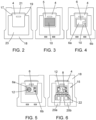
- the closed shapes labelled 21 and 23 are openings in the frame 18 which are not full of material (i.e. they are voids).
- the die paddle 4 is only attached to the surrounding frame 18 by virtue of branches 17, 19.
- the branches 17, 19 could otherwise be described as attachment points where the die paddle 4 is attached to the frame 18.
- the frame 18 may comprise an array of, for example, 20 x 5 die paddles (e.g. for a batch production process).
- first solder layer 10 is printed or dispensed onto the die paddle 4.
- first solder layer 10 is printed or dispensed onto the first major surface 5 of the die paddle 4.
- first and second components 6a, 6b of the die 6 are attached to the die paddle 4 by virtue of the first solder layer 10. This step may therefore be described as coupling the die 6 to the die paddle 4 with solder.
- the second solder layer 12 is dispensed or printed onto the die 6, specifically onto first and second components 6a, 6b.
- the clip 8 is coupled to the die (not visible in Figure 6 , it is behind the clip) by virtue of the second solder layer 12. This step may therefore be described as coupling the clip 8 to the die 6 with solder.
- a first subassembly 15 is formed.
- the first subassembly 15 comprising the die paddle 4, the die, the clip 8, and the first and second solder layers 10, 12.
- the clip 8 is initially attached to a larger strip of copper, in a similar manner to the frame 18, but is detached from said strip in advance of being attached to the die paddle 4 in the illustrated embodiment.
- the clip 8 may be said to be attached to a top of the die 6.
- the bottom of the die 6 may be said to be attached to the die paddle 4.
- the clip 8 is also attached to the surrounding frame 18 at points 20a, 20b. In a later step of the process (i.e. after Figure 9 ), the clip 8 is cut across line 22 to isolate the clip 8 from the frame 18 and define the plurality of leads 14 of the clip 8.
- the illustrated embodiment comprises the clip 8
- the clip 8 is not an essential feature of the invention.
- wirebonding may instead be used to couple a connector to the die.
- the connector may comprise one or more external leads.
- using the clip is preferable because the clip has desirable conductivity characteristics.
- the first subassembly 15 is heated.
- the process of heating the first subassembly 15 may be referred to as reflow.
- the first subassembly 15 is heated to a temperature that is greater than or equal to the melting temperature of the first and second solder layers 10, 12.
- the first subassembly 15 is heated to a temperature that is at least equal to the melting temperature of the solder (of the first and second solder layers 10, 12). This causes the first solder layer 10 and the second solder layer 12 to melt. Melting of the first and second solder layers 10, 12 can cause one or both of the first and second solder layers 10, 12 to spread.
- the first solder layer 10 may spread beyond the footprint of the die 6.
- the footprint of the die 6 may be understood to refer to the area that is bounded by the periphery of the die 6 when the first subassembly 15 is viewed in plan view (i.e., from above).
- Spreading of the first solder layer 10 may result in a limited area of the first major surface 5 of the die paddle 4 being exposed. This is because a large part of the first major surface 5 of the die paddle 4 may be covered by the first solder layer 10.
- the bond strength between the casing 16 and the die paddle 4 is proportion to the amount of the first major surface 5 of the die paddle 4 that is exposed.
- the bond strength between the cover 16 and the die paddle 4 is reduced as compared to where a larger area of the first major surface 5 is exposed. This can result in separation of the cover 16 from the die paddle 4 in use.
- the present invention seeks to address this issue, as will be discussed in more detail below.
- a protective layer 25 is applied to the first sub assembly 15.
- the protective layer 25 may be a protective material, such as a protective film.
- the protective layer 25 may be made of a highly purified water-soluble protective material, such as a water-soluble film.
- the protective layer 25 covers at least the top surfaces (when viewed in plan view) of the first sub assembly 15.
- the protective layer is preferably water soluble.
- the protective layer 25 being water soluble advantageously allows easy removal of the protective layer 25 in a later step.
- solder of the first solder layer 10 is removed from the first sub assembly 15.
- at least some of the first solder layer 10 is removed from the die paddle 4 in a region adjacent the die 6. Removal of at least some of the solder of the first solder layer 10 from the die paddle 4 in a region adjacent the die 6 exposes the die paddle 4 in that region.
- the solder of the first solder layer 10 is removed using laser ablation.
- Removing at least some of the solder from the first solder layer 10 from the die paddle 4 in a region adjacent the die 6 may be understood to refer to removing solder of the first solder layer 10 from the die paddle 4 in a region that, when the first subassembly 15 is viewed in plan view (i.e. perpendicular to the first major surface of the die paddle 4), is adjacent and outboard of the footprint of the die 6.
- the bond strength between the casing (not shown in Figures 7b and 7c - it has not yet been moulded on to the first subassembly) and the die paddle 4 is greater than the bond strength between the casing and the first solder layer 10. Therefore, exposing the die paddle 4 increases the bond strength between the casing and the first subassembly 15, which reduces the likelihood of delamination of the device 2.
- the laser ablation may also remove some of the material from the die paddle 4. Removal of the material from the die paddle 4 results in the formation of a groove 24 in the die paddle 4.
- the groove 24 can be seen in Figure 7b .
- the groove 24 further increases the bond strength between the cover 16 and the die paddle 4. This is because the surface area of the first major surface 5 of the die paddle 4 is increased by the presence of the groove 24.
- the groove 24 may extend around at least 50% of the footprint, or periphery, of the die 6. However, in some embodiments, the groove 24 may extend around less than 50% of the footprint, or periphery, of the die 6.
- the groove 24 extends about a perimeter of the die paddle 4. In some embodiments, the groove may extend about at least 50% of the perimeter of the die paddle 4.
- the groove 24 extending about a perimeter of the die paddle 4 may be understood to mean that the groove 24 is disposed inboard of the periphery of the die paddle 4.
- the groove 24 may be said to be disposed in the region, when the first subassembly 15 is viewed in plan view (i.e, perpendicular to the firs major surface 5 of the die paddle 4), which is between the periphery of the footprint of the die 6 and the periphery of the footprint of the die paddle 4.
- the depth and/or width of the groove 24 may be at least 5 ⁇ m. In some embodiments, the depth and/or width may be at least 3 ⁇ m and/or up to 15 ⁇ m.
- the width of the groove 24 may be at least 20 ⁇ m.
- the depth of the groove may be up to 10 ⁇ m.
- the width of the groove 24 may be up to 40 ⁇ m. In some embodiments, the width of the groove 24 may be greater than 40 ⁇ m. The width and/or depth of the groove 24 may be chosen based on, for example, the size of the semiconductor device 2, and the intended application of the semi-conductor device 2.
- the groove 24 define a plurality of sections 24a-c.
- the plurality of sections 24a-c comprises three sections.
- the groove 24 may define any suitable number of sections.
- the number of sections of the groove may be determined by, for example, the geometry of the die paddle 4, the die 6.
- the groove may define only a single section, or may define four or more sections.
- the sections 24a-c define a respective continuous path.
- the sections 24a-c of the groove 24 defining a respective continuous path may be understood to mean that each section 24a-c does not define any vertices.
- the sections 24a-c may extend continuously from one another. This may be understood to mean that no vertices are defined at the interfaces between the sections 24a-c of the groove 24. However, in some embodiments, one or more vertices may be defined at the interface between the sections 24a-c of the groove 24.
- each section of the groove 24 is non-linear.
- each section 24a-c of the groove 24 defines a wave formation. This further assists with the strength of the bond between the die paddle 4 and the cover (not shown in Figure 8 , it has not yet been moulded onto the first subassembly 15).
- the groove 24 may define any other suitable non-linear or linear formation.
- the sections 24a-c may not be continuous.
- one or more of the sections 24a-c of the groove 24 may be dashed, may define a zig-zag formation, or may be formed of a plurality of dots.
- a groove need not be provided, and the laser ablation may be carried out to only remove solder from the first solder layer 10. That is to say, the laser ablation does not remove any material from the die paddle 4.
- the first sub assembly 15 is washed.
- the step of washing the first subassembly 15 may be referred to as 'flux cleaning', or simply 'cleaning process'.
- the first subassembly 15 may be washed using water. Since the protective layer 25 is water soluble, washing the first subassembly 15 with water dissolves the protective layer. In other embodiments, the protective layer 25 may not be water soluble, and the first subassembly may be washed using an alternative substance. Washing the first subassembly 15 also removes any residue that may be present on the first subassembly 15 following the laser ablation.
- a casing 16 is moulded onto the first subassembly 15 such that the casing at least partly surrounds the die 6, the die paddle 4, and the clip 8.
- the casing 16 does not entirely surround all of these components, but should surround at least the exposed surfaces of the die 6 (i.e., of all components 6a, 6b of the die).
- the casing 16 may therefore be said to surround the die and at least part of the die paddle 4 and the clip 8.
- the extent to which the casing 16 covers the first subassembly 15 is indicated by the hatched markings shown in Figure 9 .
- the casing 16 is shown in a partially transparent view so as to aid the understanding of the location of the casing 16.
- the purpose of the casing 16 is to protect the die from moisture ingress and impacts.
- the casing 16 is overmoulded to the die paddle 4 by injection moulding a casing material which is able to flow.
- the material flows through a mould, not shown in Figure 9 , which defines the shape of the casing 16 once the material has set (e.g. hardened, or solidified).
- the material flows to surround the first subassembly 15, as discussed above.
- the material also flows into the groove 24.
- the groove 24 defines a locking feature into which material can extend to more robustly couple the casing 16 to the die paddle 4. This reduces the risk of the casing 16 delaminating and/or cracking.
- the first subassembly 15 is detached from the surrounding frame 18 by cutting the branches 17, 19 shown in Figure 2 .
- the leads 14 of the clip 8 are also cut and formed. Assembly of the semiconductor assembly is therefore complete.
- the solder may be removed using chemical etching instead of laser ablation. Where chemical etching is used, the method is the same as for the previous embodiment up to the reflow step.
- a protective layer is applied to the first subassembly 15. The protective layer is applied to the surfaces that no chemical etching is to take place on. Therefore, the protective layer may be applied to all visible surfaces of the first subassembly 15 excluding the first solder layer 15 in the region between the periphery of the footprint of the die 6 and the periphery of the die paddle 4.
- the chemical bath may contain a chemical capable of dissolving solder.
- the chemical contained in the bath may be an aqueous solution of 0.3M fluroboric acid with 0.2M hydrogen peroxide.
- the first subassembly is submerged for a predetermined amount of time.
- the predetermined amount of time may be, for example, at least 5 minutes and/or up to 20 minutes.
- the first subassembly 15 is removed from the chemical bath.
- the first subassembly 15 is then washed.
- Submersion in the chemical bath removes solder from the die paddle in a region adjacent the die, preferably adjacent the footprint of the die, to expose the die paddle. This allows the casing 16 to better adhere to the first subassembly 15.
- the casing 16 is then applied in the same manner as discussed above in relation to Figure 9 .
- a higher D/P ratio reduces the area of the die paddle 4 to which the casing 16 is able to adhere, said area being further reduced by solder spread. Therefore, removing solder from the first subassembly is particularly advantageous where the D/P ratio is at least 0.75.
Landscapes
- Die Bonding (AREA)
Abstract
There is disclosed a method of manufacturing a semiconductor device. The method comprises securing a die to a die paddle with solder and securing a clip to the die with solder to form a first subassembly. The method further comprises heating the first subassembly to at least the melting temperature of the solder, then subsequently removing at least some of the solder from the die paddle in a region adjacent the die to expose the die paddle in that region. The method further comprises moulding a casing on to the first subassembly such that the casing at least partly surrounds the die, the die paddle, and the clip.
Description
- The present invention relates to a method of manufacturing a semi-conductor device.
- Semiconductor assemblies, such as transistors, are manufactured as layered assemblies including components such as die paddles, dies, clips and a casing. The casing provides a protective functionality and at least partially surrounds the die and other components that form a part of the semiconductor assembly.
- Semiconductor assemblies are manufactured by bonding the components together. Once bonded, the assembly defines a laminate structure that forms a number of layers. For example, the die paddle, die(s), clip(s), and casing may each form a layer of the laminate structure.
- Semi-conductor assemblies are subject to stress in use. The stress may arise as a result of, for example, thermal expansion of the components and/or mechanical deformation. The stress to which semi-conductor assemblies are subject to can result in delamination of the components. This is undesirable because delamination can ultimately lead to failure of the assembly as a result of, for example, moisture ingress.
- There exists a need to overcome the disadvantages associated with existing methods of manufacturing semiconductor assemblies, whether mentioned in this document or otherwise.
- In a first aspect of the invention there is provided a method of manufacturing a semiconductor device. The method comprises securing a die to a die paddle with solder and securing a clip to the die with solder to form a first subassembly. The method further comprises heating the first subassembly to at least the melting temperature of the solder, then subsequently removing at least some of the solder from the die paddle in a region adjacent the die to expose the die paddle in that region. The method further comprises moulding a casing on to the first subassembly such that the casing at least partly surrounds the die, the die paddle, and the clip.
- Removing at least some of the solder from the die paddle in a region adjacent the die may be understood to refer to removing solder from the die paddle in a region that, when the first subassembly is viewed in plan view (i.e., perpendicular to a first major surface of the die paddle), is adjacent and outboard of the footprint of the die.
- Solder may be removed from the die paddle in a region that is adjacent and outboard of the footprint of the die.
- Solder is typically used in semiconductor devices to secure the components of the devices together. Liquid (molten) solder is applied to the die paddle in the region to which the die is to be secured, and the die is placed on the liquid solder to create a temporary joint. The components are then heated to a temperature above the melting temperature of the solder in a process referred to as reflow, which creates a permanent joint. During reflow, some of the solder can spread beyond the footprint of the die, covering a part of the die paddle. Following reflow, a casing, which is typically an epoxy mould compound, is moulded onto the components.
- The solder spreading beyond the footprint of the die is undesirable because the strength of the bond between the casing and the solder is less than the strength of the bond between the casing and the die paddle. Reduced bond strength increases the likelihood of delamination of the casing from the other components of the device, which ultimately leads to failure of the device due to, for example, moisture ingress. By removing at least some of the solder from the die paddle in a region adjacent the die, the strength of the bond between the casing and the first subassembly is improved. Advantageously, this reduces the likelihood of delamination of the components.
- The region of the die paddle that is exposed by removal of the solder may correspond to the region from which solder was removed.
- The solder may be removed from the die paddle using laser ablation.
- Laser ablation allows removal of the solder in an efficient manner.
- The method may further comprise, while removing at least some of the solder from the die paddle, removing at least some material from the die paddle to form a groove in the die paddle.
- Where a groove is formed in the die paddle, the surface area of the die paddle is increased. Increasing the surface area of the die paddle improves the bond strength between the casing and the die paddle. In addition, the groove acts as a locking mechanism to better secure the casing to the die paddle. Therefore, the groove further reduces the likelihood of delamination of the device.
- The groove may extend around at least 50% of the perimeter of the die paddle.
- The groove may extend around at least 25% of the perimeter of the die paddle.
- The groove extending around the perimeter of the die paddle may be understood to mean that the groove extends inboard of a periphery of the die paddle.
- The groove may extend around at least 50% of the footprint of the die. The groove may extend around at least 25% of the footprint of the die.
- Where the groove extends around at least 50% of the perimeter of the die paddle, the likelihood of delamination is reduced to a desirable amount.
- The groove may define a plurality of sections that each define a continuous path or a discontinuous path.
- The sections of the groove defining a respective continuous path may be understood to mean that the each section does not define any vertices. A vertex may be defined at the interfaces between the sections of the groove. In some embodiments, one or more of the sections may define vertices.
- A discontinuity in the groove presents a delamination risk because stress can concentrate at the discontinuity. Therefore, where the groove sections define a continuous path, the likelihood of delamination of the components is further reduced.
- The groove may be non-linear. The groove may define a wave formation.
- Where the groove is non-linear, the length, and therefore surface area, of the groove is increased as compared to if, for example, the groove were linear. Increasing the surface area of the groove increases the surface area of the die paddle, thereby increasing the bond strength between the casing and the die paddle. Increasing the bond strength between the casing and the die paddle advantageously reduces the likelihood of delamination of the device.
- Moulding the casing on to the first subassembly may comprise moulding the casing into the groove.
- The groove depth and/or width may be at least 5µm. The groove depth and/or width may be at least 3µm and/or up to 15µm. The width of the groove may be at least 20µm and/or up to 40µm. The depth of the groove may be up to 10µm.
- The method may further comprise, prior to removing at least some of the solder from the die paddle, applying a protective layer to the first subassembly.
- Where a protective film is applied to the first subassembly, the likelihood of damage to the components of the device while removing the solder from the die paddle is reduced.
- The method may further comprise after heating the first subassembly and before removing at least some of the solder from the die paddle, applying a protective layer to the first subassembly. The solder may be removed by chemical etching.
- A ratio of an area of a footprint of the die to an area of the footprint of the die paddle may be at least 0.75.
- A ratio of an area of a footprint of the die to an area of the footprint of the die paddle may be at least 0.5.
- The area of the footprint of the die may refer to the total footprint area of the die. The area of the footprint of the die paddle may refer to the total footprint area of the die paddle.
- A larger die to paddle ratio increases the likelihood of delamination because the solder can spread to a periphery of the die paddle, leaving no or very little die paddle material for the casing to bond to. Therefore, the present invention is particularly beneficial where a ratio of a cross-sectional area of the die, taken in a plane parallel to a major surface of the die, to a cross-sectional area of the die paddle, taken in a plane parallel to a major surface of the die paddle is at least 0.75. Having a larger die to paddle ratio allows for increased functionality of the device as compared to a smaller die to paddle ratio.
- Embodiments of the present application will now be described with reference to the accompanying figures, in which:
-
Figure 1 shows a cross-sectional side view of a semi-conductor device manufactured according to an embodiment of the present invention; -
Figures 2 to 7 schematically show a method of manufacturing the semi-conductor device ofFigure 1 according to an embodiment of the present invention; -
Figure 8 shows a first subassembly of the semi-conductor device ofFigure 1 ; and -
Figure 9 shows a further step in the method of manufacturing the semi-conductor device ofFigure 1 . -
Figure 1 shows asemiconductor device 2. Thesemi-conductor device 2 comprises adie paddle 4. Thesemi-conductor device 2 comprises adie 6. Thesemi-conductor device 2 comprises aclip 8. - The
die paddle 4 serves as a base of thesemi-conductor device 2 to which other components of the device are attached. Thedie paddle 4 defines a firstmajor surface 5 and a secondmajor surface 7. The secondmajor surface 7 is generally opposed to the firstmajor surface 5. Thedie paddle 4 is a generally plate-like component, and is generally quadrangular. Thedie paddle 4 forms a base in the manufacture of thedevice 2. Thedie paddle 4 is manufactured from a conductive material such as copper (including a copper alloy). - The
die 6 is secured to thedie paddle 4. Thedie 6 is secured to thedie paddle 4 by virtue of afirst solder layer 10. Although not apparent fromFigure 1 , thedie 6 comprises multiple constituent components (only one of which is visible inFigure 1 - the others are hidden by the visible component). However, in some embodiment, thedie 6 may comprise a single component. Thedie 6 is made of a semi-conducting material. Thedie 6 has a functional circuit fabricated thereon. Thedie 6 is generally rectangular but may be any other suitable shape. Thedie 6 is plate-like in shape. - The
clip 8 is formed of multipleconstituent parts part clip 8 is secured to a respective component of thedie 6. Theclip 8 is secured to thedie 6 by virtue of asecond solder layer 12. Thesecond solder layer 12 may be applied in multiple sections, each for a respective component of thedie 6, as will be discussed in more detail below. A plurality of leads 14 (only one of which is visible inFigure 1 - the rest are hidden by the lead that is visible) extend from theclip 8. Eachpart clip 8 may have at least onelead 14. The plurality ofleads 14 may be integrally formed with therespective part clip 8, or may be separately formed from theclip 8 and secured to the respective part of theclip 8 using any suitable method, such as by welding. - The
semi-conductor device 2 further comprises acover 16. Thecover 16 may also be referred to as an isolator, a casing, or an encapsulant. Thecover 16 encapsulates the remaining components of the semi-conductor device 2 (i.e., thedie paddle 4, thedie 6, and the clip 8). Thecover 16 adheres to thedie paddle 4, thedie 6, and theclip 8, which secures thecover 16 thereto. However, as will be discussed in more detail below, thecover 16 can separate from the components in use due to, for example, repeated deformation of thedevice 2. The leads 14 of theclip 8 extend through thecover 16. This allows theleads 14, and therefore thedevice 2, to be connected to the external circuit (not shown). Thecover 16 may be made from any suitable electrically isolating material, such as an epoxy. - Manufacture of the
semi-conductor device 2 will now be discussed with reference to Figures 2 to 11. - Beginning with
Figure 2 , thedie paddle 4 is shown in a form where it is still connected to a surroundingframe 18. Theframe 18 may be referred to as a lead frame. Theframe 18 is effectively a planar plate of conductive material, such as copper, from which the geometry of thedie paddle 4 is stamped or etched. As such, as shown inFigure 3 , the closed shapes labelled 21 and 23 are openings in theframe 18 which are not full of material (i.e. they are voids). As shown inFigure 2 , thedie paddle 4 is only attached to the surroundingframe 18 by virtue ofbranches branches die paddle 4 is attached to theframe 18. Theframe 18 may comprise an array of, for example, 20 x 5 die paddles (e.g. for a batch production process). - Turning to
Figure 3 , a subsequent step of the manufacture process is schematically indicated. In the step shown inFigure 3 , thefirst solder layer 10 is printed or dispensed onto thedie paddle 4. In particular, thefirst solder layer 10 is printed or dispensed onto the firstmajor surface 5 of thedie paddle 4. In a subsequent step shown inFigure 4 , first andsecond components die 6 are attached to thedie paddle 4 by virtue of thefirst solder layer 10. This step may therefore be described as coupling thedie 6 to thedie paddle 4 with solder. - In the subsequent step shown in
Figure 5 , thesecond solder layer 12 is dispensed or printed onto thedie 6, specifically onto first andsecond components - In the subsequent manufacture step shown in
Figure 6 , theclip 8 is coupled to the die (not visible inFigure 6 , it is behind the clip) by virtue of thesecond solder layer 12. This step may therefore be described as coupling theclip 8 to thedie 6 with solder. Once theclip 8 is coupled to the die, afirst subassembly 15 is formed. Thefirst subassembly 15 comprising thedie paddle 4, the die, theclip 8, and the first and second solder layers 10, 12. Theclip 8 is initially attached to a larger strip of copper, in a similar manner to theframe 18, but is detached from said strip in advance of being attached to thedie paddle 4 in the illustrated embodiment. Theclip 8 may be said to be attached to a top of thedie 6. The bottom of thedie 6 may be said to be attached to thedie paddle 4. Theclip 8 is also attached to the surroundingframe 18 atpoints Figure 9 ), theclip 8 is cut acrossline 22 to isolate theclip 8 from theframe 18 and define the plurality ofleads 14 of theclip 8. - For completeness, although the illustrated embodiment comprises the
clip 8, theclip 8 is not an essential feature of the invention. In other embodiments, wirebonding may instead be used to couple a connector to the die. The connector may comprise one or more external leads. However, using the clip is preferable because the clip has desirable conductivity characteristics. - In a subsequent step, not shown, the
first subassembly 15 is heated. The process of heating thefirst subassembly 15 may be referred to as reflow. When undergoing reflow thefirst subassembly 15 is heated to a temperature that is greater than or equal to the melting temperature of the first and second solder layers 10, 12. Put another way, thefirst subassembly 15 is heated to a temperature that is at least equal to the melting temperature of the solder (of the first and second solder layers 10, 12). This causes thefirst solder layer 10 and thesecond solder layer 12 to melt. Melting of the first and second solder layers 10, 12 can cause one or both of the first and second solder layers 10, 12 to spread. In some instances, thefirst solder layer 10 may spread beyond the footprint of thedie 6. The footprint of thedie 6 may be understood to refer to the area that is bounded by the periphery of thedie 6 when thefirst subassembly 15 is viewed in plan view (i.e., from above). Spreading of thefirst solder layer 10 may result in a limited area of the firstmajor surface 5 of thedie paddle 4 being exposed. This is because a large part of the firstmajor surface 5 of thedie paddle 4 may be covered by thefirst solder layer 10. The bond strength between thecasing 16 and thedie paddle 4 is proportion to the amount of the firstmajor surface 5 of thedie paddle 4 that is exposed. Where none, or a small amount, of the firstmajor surface 5 of thedie paddle 4 is exposed, the bond strength between thecover 16 and thedie paddle 4 is reduced as compared to where a larger area of the firstmajor surface 5 is exposed. This can result in separation of thecover 16 from thedie paddle 4 in use. The present invention seeks to address this issue, as will be discussed in more detail below. - In a subsequent step, shown in
Figure 7a , aprotective layer 25 is applied to thefirst sub assembly 15. Theprotective layer 25 may be a protective material, such as a protective film. Theprotective layer 25 may be made of a highly purified water-soluble protective material, such as a water-soluble film. Theprotective layer 25 covers at least the top surfaces (when viewed in plan view) of thefirst sub assembly 15. The protective layer is preferably water soluble. Theprotective layer 25 being water soluble advantageously allows easy removal of theprotective layer 25 in a later step. - In a subsequent step, shown in
Figures 7b and 7c , at least some of the solder of thefirst solder layer 10 is removed from thefirst sub assembly 15. In particular at least some of thefirst solder layer 10 is removed from thedie paddle 4 in a region adjacent thedie 6. Removal of at least some of the solder of thefirst solder layer 10 from thedie paddle 4 in a region adjacent thedie 6 exposes thedie paddle 4 in that region. The solder of thefirst solder layer 10 is removed using laser ablation. Removing at least some of the solder from thefirst solder layer 10 from thedie paddle 4 in a region adjacent thedie 6 may be understood to refer to removing solder of thefirst solder layer 10 from thedie paddle 4 in a region that, when thefirst subassembly 15 is viewed in plan view (i.e. perpendicular to the first major surface of the die paddle 4), is adjacent and outboard of the footprint of thedie 6. The bond strength between the casing (not shown inFigures 7b and 7c - it has not yet been moulded on to the first subassembly) and thedie paddle 4 is greater than the bond strength between the casing and thefirst solder layer 10. Therefore, exposing thedie paddle 4 increases the bond strength between the casing and thefirst subassembly 15, which reduces the likelihood of delamination of thedevice 2. - The laser ablation may also remove some of the material from the
die paddle 4. Removal of the material from thedie paddle 4 results in the formation of agroove 24 in thedie paddle 4. Thegroove 24 can be seen inFigure 7b . Thegroove 24 further increases the bond strength between thecover 16 and thedie paddle 4. This is because the surface area of the firstmajor surface 5 of thedie paddle 4 is increased by the presence of thegroove 24. In some embodiments, thegroove 24 may extend around at least 50% of the footprint, or periphery, of thedie 6. However, in some embodiments, thegroove 24 may extend around less than 50% of the footprint, or periphery, of thedie 6. Thegroove 24 extends about a perimeter of thedie paddle 4. In some embodiments, the groove may extend about at least 50% of the perimeter of thedie paddle 4. Thegroove 24 extending about a perimeter of thedie paddle 4 may be understood to mean that thegroove 24 is disposed inboard of the periphery of thedie paddle 4. Thegroove 24 may be said to be disposed in the region, when thefirst subassembly 15 is viewed in plan view (i.e, perpendicular to the firsmajor surface 5 of the die paddle 4), which is between the periphery of the footprint of thedie 6 and the periphery of the footprint of thedie paddle 4. The depth and/or width of thegroove 24 may be at least 5µm. In some embodiments, the depth and/or width may be at least 3µm and/or up to 15µm. The width of thegroove 24 may be at least 20µm. In some embodiments, the depth of the groove may be up to 10µm. In some embodiments, the width of thegroove 24 may be up to 40µm. In some embodiments, the width of thegroove 24 may be greater than 40µm. The width and/or depth of thegroove 24 may be chosen based on, for example, the size of thesemiconductor device 2, and the intended application of thesemi-conductor device 2. - Referring to
Figure 8 , thefirst subassembly 15 is shown in plan view following formation of thegroove 24. Thegroove 24 define a plurality ofsections 24a-c. In the depicted embodiment, the plurality ofsections 24a-c comprises three sections. However, in some, non-depicted, embodiments, thegroove 24 may define any suitable number of sections. The number of sections of the groove may be determined by, for example, the geometry of thedie paddle 4, thedie 6. For example, the groove may define only a single section, or may define four or more sections. Thesections 24a-c define a respective continuous path. Thesections 24a-c of thegroove 24 defining a respective continuous path may be understood to mean that eachsection 24a-c does not define any vertices. Thesections 24a-c may extend continuously from one another. This may be understood to mean that no vertices are defined at the interfaces between thesections 24a-c of thegroove 24. However, in some embodiments, one or more vertices may be defined at the interface between thesections 24a-c of thegroove 24. In the embodiment shown inFigure 8 , each section of thegroove 24 is non-linear. In particular, eachsection 24a-c of thegroove 24 defines a wave formation. This further assists with the strength of the bond between thedie paddle 4 and the cover (not shown inFigure 8 , it has not yet been moulded onto the first subassembly 15). This is because the surface area of thegroove 24 is increased where it is non-linear, as compared to if the groove were, for example, linear. In other embodiments, thegroove 24 may define any other suitable non-linear or linear formation. In some embodiments, thesections 24a-c may not be continuous. For example, one or more of thesections 24a-c of thegroove 24 may be dashed, may define a zig-zag formation, or may be formed of a plurality of dots. In some embodiments, a groove need not be provided, and the laser ablation may be carried out to only remove solder from thefirst solder layer 10. That is to say, the laser ablation does not remove any material from thedie paddle 4. - In a subsequent step, shown in
Figure 7c , thefirst sub assembly 15 is washed. The step of washing thefirst subassembly 15 may be referred to as 'flux cleaning', or simply 'cleaning process'. Thefirst subassembly 15 may be washed using water. Since theprotective layer 25 is water soluble, washing thefirst subassembly 15 with water dissolves the protective layer. In other embodiments, theprotective layer 25 may not be water soluble, and the first subassembly may be washed using an alternative substance. Washing thefirst subassembly 15 also removes any residue that may be present on thefirst subassembly 15 following the laser ablation. - In a subsequent step shown in
Figure 9 , acasing 16 is moulded onto thefirst subassembly 15 such that the casing at least partly surrounds thedie 6, thedie paddle 4, and theclip 8. Thecasing 16 does not entirely surround all of these components, but should surround at least the exposed surfaces of the die 6 (i.e., of allcomponents casing 16 may therefore be said to surround the die and at least part of thedie paddle 4 and theclip 8. The extent to which thecasing 16 covers thefirst subassembly 15 is indicated by the hatched markings shown inFigure 9 . Also, thecasing 16 is shown in a partially transparent view so as to aid the understanding of the location of thecasing 16. The purpose of thecasing 16 is to protect the die from moisture ingress and impacts. - The
casing 16 is overmoulded to thedie paddle 4 by injection moulding a casing material which is able to flow. The material flows through a mould, not shown inFigure 9 , which defines the shape of thecasing 16 once the material has set (e.g. hardened, or solidified). The material flows to surround thefirst subassembly 15, as discussed above. The material also flows into thegroove 24. As such, thegroove 24 defines a locking feature into which material can extend to more robustly couple thecasing 16 to thedie paddle 4. This reduces the risk of thecasing 16 delaminating and/or cracking. - In a subsequent step of manufacture, which is not shown in Figures 2 to 11, the
first subassembly 15 is detached from the surroundingframe 18 by cutting thebranches Figure 2 . During the cutting process, theleads 14 of theclip 8 are also cut and formed. Assembly of the semiconductor assembly is therefore complete. - In some, non-depicted, embodiments, the solder may be removed using chemical etching instead of laser ablation. Where chemical etching is used, the method is the same as for the previous embodiment up to the reflow step. Following reflow, a protective layer is applied to the
first subassembly 15. The protective layer is applied to the surfaces that no chemical etching is to take place on. Therefore, the protective layer may be applied to all visible surfaces of thefirst subassembly 15 excluding thefirst solder layer 15 in the region between the periphery of the footprint of thedie 6 and the periphery of thedie paddle 4. Following this, the first subassembly is submerged in a chemical bath. The chemical bath may contain a chemical capable of dissolving solder. For example, the chemical contained in the bath may be an aqueous solution of 0.3M fluroboric acid with 0.2M hydrogen peroxide. The first subassembly is submerged for a predetermined amount of time. The predetermined amount of time may be, for example, at least 5 minutes and/or up to 20 minutes. Following elapse of the predetermined amount of time, thefirst subassembly 15 is removed from the chemical bath. Thefirst subassembly 15 is then washed. Submersion in the chemical bath removes solder from the die paddle in a region adjacent the die, preferably adjacent the footprint of the die, to expose the die paddle. This allows thecasing 16 to better adhere to thefirst subassembly 15. Thecasing 16 is then applied in the same manner as discussed above in relation toFigure 9 . - Removal of the solder from the
die paddle 4, whether by laser ablation or chemical etching, advantageously improves adhesion between thecasing 16 and thefirst subassembly 15, in particular thecasing 16 and thedie paddle 4. As mentioned above, this is because the bond strength between thecasing 16 and thedie paddle 4 is greater than the bond strength between thecasing 16 and the solder material. It may be particularly desirable to increase the bond strength between thecasing 16 and thefirst subassembly 15, in particular thedie paddle 4, where a ratio of the area of the footprint of thedie 6 to the area of the footprint of thedie paddle 6, also referred to as the D/P ratio, is at least 0.75. A higher D/P ratio may be required depending upon the required functionality of thesemi-conductor device 2. However, a higher D/P ratio reduces the area of thedie paddle 4 to which thecasing 16 is able to adhere, said area being further reduced by solder spread. Therefore, removing solder from the first subassembly is particularly advantageous where the D/P ratio is at least 0.75. - While specific embodiments of the invention have been described above, it will be appreciated that the invention may be practiced otherwise than as described. The descriptions above are intended to be illustrative, not limiting. Thus, it will be apparent to one skilled in the art that modifications may be made to the invention as described without departing from the scope of the claims set out below.
Claims (11)
- A method of manufacturing a semiconductor device, the method comprising:securing a die to a die paddle with solder and securing a clip to the die with solder to form a first subassembly;heating the first subassembly to at least the melting temperature of the solder, then subsequently removing at least some of the solder from the die paddle in a region adjacent the die to expose the die paddle in that region; andmoulding a casing on to the first subassembly such that the casing at least partly surrounds the die, the die paddle, and the clip.
- The method of claim 1, wherein the solder is removed from the die paddle using laser ablation.
- The method of claim 2, further comprising, while removing at least some of the solder from the die paddle, removing at least some material from the die paddle to form a groove in the die paddle.
- The method of claim 3, wherein the groove extends around at least 50% of the perimeter of the die paddle.
- The method of claim 3 or claim 4, wherein the groove defines a plurality of sections that each define a continuous path or a discontinuous path.
- The method of any of claims 3 to 5, wherein the groove is non-linear; optionally wherein the groove defines a wave formation.
- The method of any of claims 3 to 6, wherein moulding the casing on to the first subassembly comprises moulding the casing into the groove.
- The method of any of claims 4 to 7, wherein the groove depth and/or width is at least 5µm.
- The method of any preceding claim, further comprising, prior to removing at least some of the solder from the die paddle, applying a protective layer to the first subassembly.
- The method of claim 1 or claim 2, further comprising, after heating the first subassembly and before removing at least some of the solder from the die paddle, applying a protective layer to the first subassembly, and wherein the solder is removed by chemical etching.
- The method of any preceding claim, wherein a ratio of an area of a footprint of the die to an area of the footprint of the die paddle is at least 0.75.
Priority Applications (3)
| Application Number | Priority Date | Filing Date | Title |
|---|---|---|---|
| EP23204877.7A EP4542645A1 (en) | 2023-10-20 | 2023-10-20 | A method of manufacturing semiconductor assemblies |
| CN202411449757.9A CN119864285A (en) | 2023-10-20 | 2024-10-17 | Method for manufacturing semiconductor assembly |
| US18/919,615 US20250132289A1 (en) | 2023-10-20 | 2024-10-18 | Method of manufacturing semiconductor assemblies |
Applications Claiming Priority (1)
| Application Number | Priority Date | Filing Date | Title |
|---|---|---|---|
| EP23204877.7A EP4542645A1 (en) | 2023-10-20 | 2023-10-20 | A method of manufacturing semiconductor assemblies |
Publications (1)
| Publication Number | Publication Date |
|---|---|
| EP4542645A1 true EP4542645A1 (en) | 2025-04-23 |
Family
ID=88506807
Family Applications (1)
| Application Number | Title | Priority Date | Filing Date |
|---|---|---|---|
| EP23204877.7A Pending EP4542645A1 (en) | 2023-10-20 | 2023-10-20 | A method of manufacturing semiconductor assemblies |
Country Status (3)
| Country | Link |
|---|---|
| US (1) | US20250132289A1 (en) |
| EP (1) | EP4542645A1 (en) |
| CN (1) | CN119864285A (en) |
Citations (8)
| Publication number | Priority date | Publication date | Assignee | Title |
|---|---|---|---|---|
| US20070114676A1 (en) * | 2005-11-18 | 2007-05-24 | Semiconductor Components Industries, Llc. | Semiconductor package structure and method of manufacture |
| US20140151866A1 (en) * | 2012-11-30 | 2014-06-05 | Infineon Technologies Ag | Packaged Semiconductor Device with Tensile Stress and Method of Making a Packaged Semiconductor Device with Tensile Stress |
| WO2014159471A1 (en) * | 2013-03-14 | 2014-10-02 | Vishay-Siliconix | Stack die package |
| US20170162403A1 (en) * | 2013-03-14 | 2017-06-08 | Vishay-Siliconix | Method for fabricating stack die package |
| US20190371710A1 (en) * | 2018-05-29 | 2019-12-05 | Shindengen Electric Manufacturing Co., Ltd. | Semiconductor module having a grooved clip frame |
| US20200365549A1 (en) * | 2019-05-16 | 2020-11-19 | Infineon Technologies Ag | Clip Having Locking Recess |
| US20230170322A1 (en) * | 2021-11-29 | 2023-06-01 | Texas Instruments Incorporated | Gang clip with mount compound arrester |
| US20230187296A1 (en) * | 2021-12-10 | 2023-06-15 | Stmicroelectronics S.R.L. | Die attachment method for semiconductor devices and corresponding semiconductor device |
-
2023
- 2023-10-20 EP EP23204877.7A patent/EP4542645A1/en active Pending
-
2024
- 2024-10-17 CN CN202411449757.9A patent/CN119864285A/en active Pending
- 2024-10-18 US US18/919,615 patent/US20250132289A1/en active Pending
Patent Citations (8)
| Publication number | Priority date | Publication date | Assignee | Title |
|---|---|---|---|---|
| US20070114676A1 (en) * | 2005-11-18 | 2007-05-24 | Semiconductor Components Industries, Llc. | Semiconductor package structure and method of manufacture |
| US20140151866A1 (en) * | 2012-11-30 | 2014-06-05 | Infineon Technologies Ag | Packaged Semiconductor Device with Tensile Stress and Method of Making a Packaged Semiconductor Device with Tensile Stress |
| WO2014159471A1 (en) * | 2013-03-14 | 2014-10-02 | Vishay-Siliconix | Stack die package |
| US20170162403A1 (en) * | 2013-03-14 | 2017-06-08 | Vishay-Siliconix | Method for fabricating stack die package |
| US20190371710A1 (en) * | 2018-05-29 | 2019-12-05 | Shindengen Electric Manufacturing Co., Ltd. | Semiconductor module having a grooved clip frame |
| US20200365549A1 (en) * | 2019-05-16 | 2020-11-19 | Infineon Technologies Ag | Clip Having Locking Recess |
| US20230170322A1 (en) * | 2021-11-29 | 2023-06-01 | Texas Instruments Incorporated | Gang clip with mount compound arrester |
| US20230187296A1 (en) * | 2021-12-10 | 2023-06-15 | Stmicroelectronics S.R.L. | Die attachment method for semiconductor devices and corresponding semiconductor device |
Also Published As
| Publication number | Publication date |
|---|---|
| CN119864285A (en) | 2025-04-22 |
| US20250132289A1 (en) | 2025-04-24 |
Similar Documents
| Publication | Publication Date | Title |
|---|---|---|
| US6911353B2 (en) | Semiconductor device and method of manufacturing same | |
| TW544883B (en) | Manufacturing method of semiconductor device | |
| TWI358114B (en) | Leadless semiconductor package and method of manuf | |
| US8749035B2 (en) | Lead carrier with multi-material print formed package components | |
| HK1213690A1 (en) | Semiconductor device and method for manufacturing same | |
| US20040058478A1 (en) | Taped lead frames and methods of making and using the same in semiconductor packaging | |
| CN103843133B (en) | Lead carrier with heat-fused package components | |
| US6613607B2 (en) | Method for manufacturing encapsulated electronic components, particularly integrated circuits | |
| KR20040028799A (en) | Semiconductor package manufacturing method and semiconductor package | |
| EP0693779B1 (en) | Resin sealing type semiconductor device and method of making the same | |
| JPH05243457A (en) | Semiconductor element structure, metallic plate producing method and current transmitting terminal producing method | |
| US20200203243A1 (en) | Universal leaded/leadless chip scale package for microelecronic devices | |
| KR20150079592A (en) | Lead carrier with print-formed terminal pads | |
| KR100214552B1 (en) | Carrier frame and substrate and method for manufacture ball grid array and the use | |
| US20250132289A1 (en) | Method of manufacturing semiconductor assemblies | |
| JP4363324B2 (en) | Semiconductor module | |
| US20200203184A1 (en) | Multirow gull-wing package for microelecronic devices | |
| EP1003213A2 (en) | Method of fabricating resin-sealed semiconductor devices | |
| EP1676308B1 (en) | Electronic device and method of manufacturing thereof | |
| JP2012182209A (en) | Lead frame substrate for led element and method for manufacturing the same | |
| JP2008108967A (en) | Lead frame and semiconductor package manufacturing method using the same | |
| JPH0450749B2 (en) | ||
| HK1058645A (en) | Method for manufacturing encapsulated electronic components | |
| JP2004186644A (en) | How to separate electronic components individually | |
| HK1044737B (en) | Method for manufacturing encapsulated electronical components |
Legal Events
| Date | Code | Title | Description |
|---|---|---|---|
| PUAI | Public reference made under article 153(3) epc to a published international application that has entered the european phase |
Free format text: ORIGINAL CODE: 0009012 |
|
| STAA | Information on the status of an ep patent application or granted ep patent |
Free format text: STATUS: THE APPLICATION HAS BEEN PUBLISHED |
|
| AK | Designated contracting states |
Kind code of ref document: A1 Designated state(s): AL AT BE BG CH CY CZ DE DK EE ES FI FR GB GR HR HU IE IS IT LI LT LU LV MC ME MK MT NL NO PL PT RO RS SE SI SK SM TR |
|
| STAA | Information on the status of an ep patent application or granted ep patent |
Free format text: STATUS: REQUEST FOR EXAMINATION WAS MADE |
|
| 17P | Request for examination filed |
Effective date: 20251019 |