EP4542629A1 - Method of manufacturing semiconductor devices and corresponding semiconductor device - Google Patents
Method of manufacturing semiconductor devices and corresponding semiconductor device Download PDFInfo
- Publication number
- EP4542629A1 EP4542629A1 EP24207010.0A EP24207010A EP4542629A1 EP 4542629 A1 EP4542629 A1 EP 4542629A1 EP 24207010 A EP24207010 A EP 24207010A EP 4542629 A1 EP4542629 A1 EP 4542629A1
- Authority
- EP
- European Patent Office
- Prior art keywords
- die pad
- die
- peripheral portion
- electrically insulating
- recessed
- Prior art date
- Legal status (The legal status is an assumption and is not a legal conclusion. Google has not performed a legal analysis and makes no representation as to the accuracy of the status listed.)
- Pending
Links
Images


Classifications
-
- H—ELECTRICITY
- H10—SEMICONDUCTOR DEVICES; ELECTRIC SOLID-STATE DEVICES NOT OTHERWISE PROVIDED FOR
- H10W—GENERIC PACKAGES, INTERCONNECTIONS, CONNECTORS OR OTHER CONSTRUCTIONAL DETAILS OF DEVICES COVERED BY CLASS H10
- H10W70/00—Package substrates; Interposers; Redistribution layers [RDL]
- H10W70/40—Leadframes
- H10W70/411—Chip-supporting parts, e.g. die pads
- H10W70/417—Bonding materials between chips and die pads
-
- H—ELECTRICITY
- H10—SEMICONDUCTOR DEVICES; ELECTRIC SOLID-STATE DEVICES NOT OTHERWISE PROVIDED FOR
- H10W—GENERIC PACKAGES, INTERCONNECTIONS, CONNECTORS OR OTHER CONSTRUCTIONAL DETAILS OF DEVICES COVERED BY CLASS H10
- H10W70/00—Package substrates; Interposers; Redistribution layers [RDL]
- H10W70/40—Leadframes
- H10W70/411—Chip-supporting parts, e.g. die pads
-
- H—ELECTRICITY
- H10—SEMICONDUCTOR DEVICES; ELECTRIC SOLID-STATE DEVICES NOT OTHERWISE PROVIDED FOR
- H10W—GENERIC PACKAGES, INTERCONNECTIONS, CONNECTORS OR OTHER CONSTRUCTIONAL DETAILS OF DEVICES COVERED BY CLASS H10
- H10W95/00—Packaging processes not covered by the other groups of this subclass
-
- H—ELECTRICITY
- H10—SEMICONDUCTOR DEVICES; ELECTRIC SOLID-STATE DEVICES NOT OTHERWISE PROVIDED FOR
- H10W—GENERIC PACKAGES, INTERCONNECTIONS, CONNECTORS OR OTHER CONSTRUCTIONAL DETAILS OF DEVICES COVERED BY CLASS H10
- H10W70/00—Package substrates; Interposers; Redistribution layers [RDL]
- H10W70/01—Manufacture or treatment
- H10W70/04—Manufacture or treatment of leadframes
-
- H—ELECTRICITY
- H10—SEMICONDUCTOR DEVICES; ELECTRIC SOLID-STATE DEVICES NOT OTHERWISE PROVIDED FOR
- H10W—GENERIC PACKAGES, INTERCONNECTIONS, CONNECTORS OR OTHER CONSTRUCTIONAL DETAILS OF DEVICES COVERED BY CLASS H10
- H10W70/00—Package substrates; Interposers; Redistribution layers [RDL]
- H10W70/01—Manufacture or treatment
- H10W70/04—Manufacture or treatment of leadframes
- H10W70/042—Etching
-
- H—ELECTRICITY
- H10—SEMICONDUCTOR DEVICES; ELECTRIC SOLID-STATE DEVICES NOT OTHERWISE PROVIDED FOR
- H10W—GENERIC PACKAGES, INTERCONNECTIONS, CONNECTORS OR OTHER CONSTRUCTIONAL DETAILS OF DEVICES COVERED BY CLASS H10
- H10W70/00—Package substrates; Interposers; Redistribution layers [RDL]
- H10W70/01—Manufacture or treatment
- H10W70/04—Manufacture or treatment of leadframes
- H10W70/045—Cleaning
-
- H—ELECTRICITY
- H10—SEMICONDUCTOR DEVICES; ELECTRIC SOLID-STATE DEVICES NOT OTHERWISE PROVIDED FOR
- H10W—GENERIC PACKAGES, INTERCONNECTIONS, CONNECTORS OR OTHER CONSTRUCTIONAL DETAILS OF DEVICES COVERED BY CLASS H10
- H10W70/00—Package substrates; Interposers; Redistribution layers [RDL]
- H10W70/40—Leadframes
-
- H—ELECTRICITY
- H10—SEMICONDUCTOR DEVICES; ELECTRIC SOLID-STATE DEVICES NOT OTHERWISE PROVIDED FOR
- H10W—GENERIC PACKAGES, INTERCONNECTIONS, CONNECTORS OR OTHER CONSTRUCTIONAL DETAILS OF DEVICES COVERED BY CLASS H10
- H10W70/00—Package substrates; Interposers; Redistribution layers [RDL]
- H10W70/40—Leadframes
- H10W70/421—Shapes or dispositions
-
- H—ELECTRICITY
- H10—SEMICONDUCTOR DEVICES; ELECTRIC SOLID-STATE DEVICES NOT OTHERWISE PROVIDED FOR
- H10W—GENERIC PACKAGES, INTERCONNECTIONS, CONNECTORS OR OTHER CONSTRUCTIONAL DETAILS OF DEVICES COVERED BY CLASS H10
- H10W70/00—Package substrates; Interposers; Redistribution layers [RDL]
- H10W70/40—Leadframes
- H10W70/421—Shapes or dispositions
- H10W70/424—Cross-sectional shapes
- H10W70/427—Bent parts
- H10W70/429—Bent parts being the outer leads
-
- H—ELECTRICITY
- H10—SEMICONDUCTOR DEVICES; ELECTRIC SOLID-STATE DEVICES NOT OTHERWISE PROVIDED FOR
- H10W—GENERIC PACKAGES, INTERCONNECTIONS, CONNECTORS OR OTHER CONSTRUCTIONAL DETAILS OF DEVICES COVERED BY CLASS H10
- H10W70/00—Package substrates; Interposers; Redistribution layers [RDL]
- H10W70/40—Leadframes
- H10W70/456—Materials
- H10W70/458—Materials of insulating layers on leadframes
-
- H—ELECTRICITY
- H10—SEMICONDUCTOR DEVICES; ELECTRIC SOLID-STATE DEVICES NOT OTHERWISE PROVIDED FOR
- H10W—GENERIC PACKAGES, INTERCONNECTIONS, CONNECTORS OR OTHER CONSTRUCTIONAL DETAILS OF DEVICES COVERED BY CLASS H10
- H10W72/00—Interconnections or connectors in packages
- H10W72/071—Connecting or disconnecting
-
- H—ELECTRICITY
- H10—SEMICONDUCTOR DEVICES; ELECTRIC SOLID-STATE DEVICES NOT OTHERWISE PROVIDED FOR
- H10W—GENERIC PACKAGES, INTERCONNECTIONS, CONNECTORS OR OTHER CONSTRUCTIONAL DETAILS OF DEVICES COVERED BY CLASS H10
- H10W72/00—Interconnections or connectors in packages
- H10W72/20—Bump connectors, e.g. solder bumps or copper pillars; Dummy bumps; Thermal bumps
-
- H—ELECTRICITY
- H10—SEMICONDUCTOR DEVICES; ELECTRIC SOLID-STATE DEVICES NOT OTHERWISE PROVIDED FOR
- H10W—GENERIC PACKAGES, INTERCONNECTIONS, CONNECTORS OR OTHER CONSTRUCTIONAL DETAILS OF DEVICES COVERED BY CLASS H10
- H10W74/00—Encapsulations, e.g. protective coatings
- H10W74/01—Manufacture or treatment
-
- H—ELECTRICITY
- H10—SEMICONDUCTOR DEVICES; ELECTRIC SOLID-STATE DEVICES NOT OTHERWISE PROVIDED FOR
- H10W—GENERIC PACKAGES, INTERCONNECTIONS, CONNECTORS OR OTHER CONSTRUCTIONAL DETAILS OF DEVICES COVERED BY CLASS H10
- H10W74/00—Encapsulations, e.g. protective coatings
- H10W74/01—Manufacture or treatment
- H10W74/016—Manufacture or treatment using moulds
-
- H—ELECTRICITY
- H10—SEMICONDUCTOR DEVICES; ELECTRIC SOLID-STATE DEVICES NOT OTHERWISE PROVIDED FOR
- H10W—GENERIC PACKAGES, INTERCONNECTIONS, CONNECTORS OR OTHER CONSTRUCTIONAL DETAILS OF DEVICES COVERED BY CLASS H10
- H10W74/00—Encapsulations, e.g. protective coatings
- H10W74/10—Encapsulations, e.g. protective coatings characterised by their shape or disposition
- H10W74/111—Encapsulations, e.g. protective coatings characterised by their shape or disposition the semiconductor body being completely enclosed
- H10W74/114—Encapsulations, e.g. protective coatings characterised by their shape or disposition the semiconductor body being completely enclosed by a substrate and the encapsulations
-
- H—ELECTRICITY
- H10—SEMICONDUCTOR DEVICES; ELECTRIC SOLID-STATE DEVICES NOT OTHERWISE PROVIDED FOR
- H10W—GENERIC PACKAGES, INTERCONNECTIONS, CONNECTORS OR OTHER CONSTRUCTIONAL DETAILS OF DEVICES COVERED BY CLASS H10
- H10W74/00—Encapsulations, e.g. protective coatings
- H10W74/10—Encapsulations, e.g. protective coatings characterised by their shape or disposition
- H10W74/111—Encapsulations, e.g. protective coatings characterised by their shape or disposition the semiconductor body being completely enclosed
- H10W74/127—Encapsulations, e.g. protective coatings characterised by their shape or disposition the semiconductor body being completely enclosed characterised by arrangements for sealing or adhesion
-
- H—ELECTRICITY
- H10—SEMICONDUCTOR DEVICES; ELECTRIC SOLID-STATE DEVICES NOT OTHERWISE PROVIDED FOR
- H10W—GENERIC PACKAGES, INTERCONNECTIONS, CONNECTORS OR OTHER CONSTRUCTIONAL DETAILS OF DEVICES COVERED BY CLASS H10
- H10W70/00—Package substrates; Interposers; Redistribution layers [RDL]
- H10W70/40—Leadframes
- H10W70/421—Shapes or dispositions
- H10W70/424—Cross-sectional shapes
-
- H—ELECTRICITY
- H10—SEMICONDUCTOR DEVICES; ELECTRIC SOLID-STATE DEVICES NOT OTHERWISE PROVIDED FOR
- H10W—GENERIC PACKAGES, INTERCONNECTIONS, CONNECTORS OR OTHER CONSTRUCTIONAL DETAILS OF DEVICES COVERED BY CLASS H10
- H10W72/00—Interconnections or connectors in packages
- H10W72/50—Bond wires
- H10W72/531—Shapes of wire connectors
- H10W72/536—Shapes of wire connectors the connected ends being ball-shaped
-
- H—ELECTRICITY
- H10—SEMICONDUCTOR DEVICES; ELECTRIC SOLID-STATE DEVICES NOT OTHERWISE PROVIDED FOR
- H10W—GENERIC PACKAGES, INTERCONNECTIONS, CONNECTORS OR OTHER CONSTRUCTIONAL DETAILS OF DEVICES COVERED BY CLASS H10
- H10W72/00—Interconnections or connectors in packages
- H10W72/851—Dispositions of multiple connectors or interconnections
- H10W72/874—On different surfaces
- H10W72/884—Die-attach connectors and bond wires
-
- H—ELECTRICITY
- H10—SEMICONDUCTOR DEVICES; ELECTRIC SOLID-STATE DEVICES NOT OTHERWISE PROVIDED FOR
- H10W—GENERIC PACKAGES, INTERCONNECTIONS, CONNECTORS OR OTHER CONSTRUCTIONAL DETAILS OF DEVICES COVERED BY CLASS H10
- H10W74/00—Encapsulations, e.g. protective coatings
- H10W74/10—Encapsulations, e.g. protective coatings characterised by their shape or disposition
-
- H—ELECTRICITY
- H10—SEMICONDUCTOR DEVICES; ELECTRIC SOLID-STATE DEVICES NOT OTHERWISE PROVIDED FOR
- H10W—GENERIC PACKAGES, INTERCONNECTIONS, CONNECTORS OR OTHER CONSTRUCTIONAL DETAILS OF DEVICES COVERED BY CLASS H10
- H10W74/00—Encapsulations, e.g. protective coatings
- H10W74/10—Encapsulations, e.g. protective coatings characterised by their shape or disposition
- H10W74/111—Encapsulations, e.g. protective coatings characterised by their shape or disposition the semiconductor body being completely enclosed
-
- H—ELECTRICITY
- H10—SEMICONDUCTOR DEVICES; ELECTRIC SOLID-STATE DEVICES NOT OTHERWISE PROVIDED FOR
- H10W—GENERIC PACKAGES, INTERCONNECTIONS, CONNECTORS OR OTHER CONSTRUCTIONAL DETAILS OF DEVICES COVERED BY CLASS H10
- H10W90/00—Package configurations
- H10W90/701—Package configurations characterised by the relative positions of pads or connectors relative to package parts
- H10W90/731—Package configurations characterised by the relative positions of pads or connectors relative to package parts of die-attach connectors
- H10W90/734—Package configurations characterised by the relative positions of pads or connectors relative to package parts of die-attach connectors between a chip and a stacked insulating package substrate, interposer or RDL
-
- H—ELECTRICITY
- H10—SEMICONDUCTOR DEVICES; ELECTRIC SOLID-STATE DEVICES NOT OTHERWISE PROVIDED FOR
- H10W—GENERIC PACKAGES, INTERCONNECTIONS, CONNECTORS OR OTHER CONSTRUCTIONAL DETAILS OF DEVICES COVERED BY CLASS H10
- H10W90/00—Package configurations
- H10W90/701—Package configurations characterised by the relative positions of pads or connectors relative to package parts
- H10W90/751—Package configurations characterised by the relative positions of pads or connectors relative to package parts of bond wires
- H10W90/754—Package configurations characterised by the relative positions of pads or connectors relative to package parts of bond wires between a chip and a stacked insulating package substrate, interposer or RDL
Definitions
- the description relates to semiconductor devices.
- One or more embodiments can be applied to semiconductor devices including integrated circuits (ICs), for instance.
- ICs integrated circuits
- Resin leaks or flashes at the bottom surface of the die pad that can undesirably result from the molding step and may cause inadequate plating of the bottom surface of the die pad.
- Resin flashes may be removed via de-flashing processes such as dry de-flashing via laser ablation, for instance, or chemical de-flashing.
- Document US 2007126092 A1 discloses a package to encase a semiconductor package that is manufactured by the following steps.
- First, an electrically conductive frame is provided.
- the frame has a plurality of leadframes arranged in a matrix with each leadframe having a plurality of spaced leads extending outwardly from a central aperture.
- the electrically conductive frame further includes a plurality of connecting bars joining outer end portions of adjacent ones of the leadframes.
- a groove is formed in the connecting bars to form a reduced thickness portion between the outer end portions of adjacent ones of the leadframes.
- Third, a semiconductor device is electrically coupled to inner portions of said leads.
- Fourth, the frame and the semiconductor devices are encapsulated in a molding compound. Finally, the molding compound and the frame are cut along the grooves to form singulated semiconductor packages having outer lead portions with a height greater than the height of the reduced thickness portion.
- Document JP 2000260911 A discloses a device having a rear surface heat dissipation semiconductor resin sealed package, and a manufacturing method thereof, in which the mold resin is prevented surely from being stripped off from a rear surface heat sink or a semiconductor element.
- a semiconductor element is mounted on a rear surface heat sink disposed on the mounting board and a lead terminal is disposed on the side of the rear surface heat sink.
- the rear surface heat sink, the semiconductor element and the lead terminal are coated with a mold resin and the rear surface heat sink is exposed.
- a bend directing toward the inside of the mold resin is provided at the end of the rear surface heat sink and a recess is made at the base point of the bend on the side opposite to the mounting board.
- Document JP 2004104155 A discloses a method to provide a semiconductor device with improved adhesive strength between a die pad and sealing resin and improved moisture resistance, and a manufacturing method thereof.
- the semiconductor device is provided with a plurality of protrusions at side faces of the die pad, and a lead frame is processed so that the protrusions are bent to the mounting surface side for a semiconductor element. Further, with the semiconductor element mounted on the mounting surface and with the exposing surface of the die pad exposed, the semiconductor element, the protrusions, and inner leads etc. are sealed with the sealing resin. The protrusions and their connecting parts are engaged with the sealing resin, resulting in improvement of adhesion. During mounting, the deformation of the die pad is small, so after mounting, the good moisture resistance can also be maintained.
- Documents such as JP 2012244038 A , US 11264309 B2 , US 2013075881 A1 , US 20200273813 A1 , US 20110266662 A1 , JP 2017079229 A , US 20220093494 A1 , US 10366943 B2 , US 10784186 B2 , US 7262491 B2 and US 20230187296 A1 provide background information in the related technological area.
- An object of one or more embodiments is to overcome the drawbacks discussed in the foregoing.
- One or more embodiments relate to a corresponding (integrated circuit) semiconductor device.
- laser beam energy is applied to the bottom surface of a die pad to form therein a recessed portion that is subsequently filled with electrically insulating molding compound.
- a roughened surface is formed at the recessed portion of the die pad that enhances adhesion between the molding compound and the die pad.
- an adhesion promoter layer possibly provided at the bottom surface of the die pad is removed at the recessed portion thereof via laser ablation, prior to molding an electrically insulating encapsulation.
- Solutions as described herein may advantageously be applied to (integrated circuit) semiconductor devices provided with an exposed pad quad flat package (QFP), for instance.
- QFP quad flat package
- Figure 1 is a cross-sectional view illustrative of an (integrated circuit, IC) semiconductor device 10 provided with a quad flat package (QFP).
- IC integrated circuit
- QFP quad flat package
- the exemplary device 10 illustrated in Figure 1 comprises:
- leadframe (or “lead frame”) is currently used (see, for instance the USPC Consolidated Glossary of the United States Patent and Trademark Office) to indicate a metal frame that provides support for an integrated circuit chip or die as well as electrical leads to interconnect the integrated circuit in the die or chip to other electrical components or contacts.
- a leadframe comprises an array of electrically-conductive formations (or leads 12B) that from an outline location extend inwardly in the direction of a semiconductor chip or die 14 thus forming an array of electrically-conductive formations from a die pad 12A configured to have at least one (integrated circuit - IC) semiconductor die attached thereon.
- This may be via conventional means such as a die attach adhesive (a die attach film, for instance, as illustrated in Figure 4 and referenced therein with the reference DA).
- a semiconductor device 10 may be provided with a die pad 12A having a (central) die mounting region 120A and a raised rim 122A around the die mounting region giving the die pad 12A a vat-like shape.
- an (integrated circuit) semiconductor device such as the device 10 may also comprise electrically conductive formations 16 (wires, for instance) that couple the semiconductor die 14 to the leads (outer pads) 12B (providing input/output signals, for instance) and/or to the die pad 12A (providing a ground level, for instance) .
- An electrically insulating molding compound 20 (an epoxy resin, for instance) is molded onto the assembly in order to provide the semiconductor device 10 with a protective, electrically insulating encapsulation.
- a semiconductor device 10 as illustrated in Figure 1 is configured to be mounted on a support such as a printed circuit board (PCB), for instance.
- a support such as a printed circuit board (PCB), for instance.
- solder material solder material, for instance may be provided at the bottom surface of the die pad 12A.
- Figures 2 and 3 (wherein Figure 3 is an enlarged view of the portion of Figure 2 indicated by the arrow III) illustrate the bottom surface of a die pad 12A of a (IC) semiconductor device such as the device 10 illustrated in Figure 1 .
- a molding step as mentioned in the foregoing may undesirably result in some leaks of molding compound 20 (oftentimes referred to as molding/resin flashes) covering the bottom surface of the of the die pad 12A, at the peripheral region thereof.
- grooves G are provided at the bottom surface of the die pad 12A.
- two grooves G are provided as trenches running along the periphery of the die mounting location 120A, close to its edge, to contain resin flashes.
- Resin flashes may cause inadequate plating of solder material on the bottom surface of the die pad 12A and, consequently, may give rise to issues related to mounting/soldering on the final substrate (a PCB, for instance).
- resin flashes as illustrated, for instance, in Figure 3 may cause so-called "tin islands” (where the reference to tin is merely due to a commonly used solder material) to form.
- tin islands where the reference to tin is merely due to a commonly used solder material
- soldering material that is plated in regions of the bottom surface of the die pad 12A (at the periphery thereof, for instance) left uncovered by the molding compound 20 leaks; these "lumps” of soldering material are prone to detach from the die pad 12A (during processing, for instance) possibly causing undesired short circuits between the leads 12B, for instance, thus causing failure of the device.
- de-flashing processes that involve removing resin flashes formed at the bottom surface of the die pad 12A.
- de-flashing processes such as chemical or dry de-flashing processes may undesirably reduce adhesion of the molding compound 20 to the metallic (copper, for instance) leadframe possibly causing delamination of the molding compound 20.
- Delamination of the molding compound 20 from the die pad 12A or lead 12B may cause humidity or contaminants to enter the package possibly reaching the semiconductor die 14 and causing failure of the device 10.
- delamination caused by chemical de-flashing may be more severe when adhesion promoters (such as non-etching adhesion promoters, NEAP) are used to enhance adhesion between the molding compound 20 and the leadframe 12A, 12B.
- adhesion promoters such as non-etching adhesion promoters, NEAP
- Figure 4 is an enlarged view of the portion of Figure 1 indicated by the arrow IV that illustrates an adhesion promoter (NEAP, for instance) layer 100 provided at the interface between the molding compound 20 and the leadframe 12A, 12B.
- NEAP adhesion promoter
- the adhesion promoter layer 100 may be at least partly dissolved when devices 10 are processed in a de-flashing bath, possibly causing delamination issues. It is observed that delamination is more likely to start at a line D, that is the points at the interface between the die pad 12A and the molding compound 20 that are exposed to a de-flashing bath.
- a dry de-flashing process can be used to remove molding compound flashes at the bottom surface of the die pad 12A.
- Dry de-flashing may involve applying laser beam energy to the bottom surface of the die pad 12A to remove the undesired resin flashes via laser ablation.
- laser ablation does not conventionally extend to the edge of the back/bottom surface of the die pad 12A exposed at the bottom of the device 10.
- laser beam energy is not applied to a "safety" zone S (of about 100 microns, for instance) at the periphery of the back/bottom surface of the die pad 12A exposed at the bottom surface of the device 10 (on the right of the interface line D in Figure 4 ) in order not to undesirably ablate molding compound 20 forming the electrically insulating encapsulation (on the left of the interface line D in Figure 4 ).
- Solutions as described herein involve applying laser beam energy to the bottom surface of a die pad to form therein a recessed portion that is subsequently filled with electrically insulating material during molding.
- a roughened surface may be formed at the recessed portion of the die pad that enhances adhesion between the molding compound and the die pad.
- an adhesion promoter layer possibly provided at the bottom surface of the die pad is removed at the recessed portion thereof via laser ablation, prior to molding an electrically insulating encapsulation.
- Solutions as described herein may advantageously be applied to (integrated circuit) semiconductor devices provided with an exposed pad quad flat package (QFP) as the semiconductor device 10 illustrated in Figure 1 , for instance.
- QFP quad flat package
- Figures 5A and 5B are illustrative of processing steps according to embodiments of the present description applied to a semiconductor device such as the semiconductor device 10 exemplified in Figure 1 .
- a plurality of semiconductor devices can be concurrently processed by providing a common substrate (such as a leadframe reel or panel, for instance) comprising a plurality of individual substrates/leadframes.
- a common substrate such as a leadframe reel or panel, for instance
- Individual leadframes may be held together via connecting bars (or dam bar) running around the periphery of each (individual) leadframe.
- a final singulation step removes the connecting bars (dam bars) to obtain a plurality of individual semiconductor devices.
- solutions as described herein may be applied, for instance, also in case of other packages having an exposed die pad such as quad flat no leads packages (QFN) and/or to leadframes having no downset between the die pad 12A and the leads 12B and/or to die pads 12A not having a raised rim 122A.
- QFN quad flat no leads packages
- Figure 5A is illustrative of a semiconductor die 14 mounted (via die attach material DA, for instance) at the top/front surface of a die pad 12A, at a die mounting region 120A thereof.
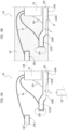
- laser beam energy LB is applied to the back/bottom surface of the die pad 12A, at the periphery of the bottom surface of the die pad 12A to form therein a recessed portion 1000. That is, metallic material (copper, for instance) of the die pad 12A is removed from the back/bottom surface thereof via laser ablation to form a recessed portion 1000 along the periphery of the back/bottom surface of the die pad 12A.
- the recessed peripheral portion 1000 of the back/bottom surface of the die pad 12A may be formed with a depth, indicated with the reference T in Figure 5A , in the range of 25 to 35 microns, for instance.
- an adhesion promoter layer (a NEAP layer, for instance) is provided on the surface of the leadframe (that is, the die pad 12A and the leads 12B), both at the top/front and back/bottom surfaces of the leadframe, as illustrated in Figure 5A .
- applying laser beam energy LB to form the peripheral recessed region 1000 of the back/bottom surface of the die pad 12A results in the adhesion promoter layer 100 being removed (ablated) at the peripheral recessed region 1000.
- the recessed peripheral portion of the second surface of the die pad 12A is exempt from the adhesion promoter layer 100 in response to the laser beam energy LB applied thereto.
- Figure 5B is illustrative of a molding step where an electrically insulating encapsulation material 20 (such as an epoxy resin, for instance) is molded onto the substrate (a leadframe, for instance) 12A, 12B having a semiconductor die 14 mounted thereon, subsequently to forming the recessed portion 1000 as described in the foregoing.
- an electrically insulating encapsulation material 20 such as an epoxy resin, for instance
- the (electrically insulating) molding compound 20 fills the recessed peripheral portion 1000 of the back/bottom surface of the die pad 12A thus forming a layer (having a thickness notionally equal to the depth T of the recessed portion 1000) of encapsulation material 20 that covers the back/bottom surface of the die pad 12A at the recessed portion 1000.
- the bottom surface of a device 10 comprises:
- the peripheral rim 122A is embedded in the encapsulation material 20.
- a peripheral recessed region 1000 formed at the die mounting region 120A counters undesired leakage of molding material over the central portion of the back/bottom surface of the die pad 12A.
- the recessed peripheral portion 1000 of the back/bottom surface of the die pad 12A may be formed with a depth, in the range of 25 to 35 microns, for instance.
- Relatively shallow recessed peripheral portions 1000 having a depth, for instance, between 2 and 3 microns, may also be formed that have been observed to give satisfactory results in terms of countering undesired leakage of molding material over the central portion of the back/bottom surface of the die pad 12A.
- a de-flashing step (a per se conventional de-flashing step such as chemical de-flashing step, for instance) may be performed subsequent to the molding step.
- a de-flashing step does not completely remove the (electrically insulating) molding compound 20 that fills the recessed peripheral portion 1000 also in embodiments where the layer of encapsulation material 20 at the recessed portion 1000 has a thickness between 2 and 3 microns. Said otherwise, a de-flashing step leaves the die pad 12A material (copper, for instance) at the recessed peripheral portion 1000 covered with a layer of encapsulation material 20 (possibly with a thickness between 2 and 3 microns) .
- applying laser beam energy LB to form a peripheral recessed portion 1000 as illustrated in the figures has the effect of roughening the back/bottom surface of the die mounting region 120A at the peripheral recessed portion 1000.
- a surface being "roughened” indicates that such a surface is made rough.
- solutions as described herein in relation to Figures 5A, 5B and 6 involve molding an encapsulation 20 of electrically insulating material (an epoxy resin, for instance) onto a substrate (such as a leadframe comprising die pad 12A and leads 12B) having at (least one) semiconductor die 14 arranged thereon.
- electrically insulating material an epoxy resin, for instance
- the semiconductor die 14 is arranged at a die mounting region 120A at a first (top/front) surface of a die pad 12A in the substrate, wherein the die pad 12A having a second (bottom/back) surface opposite the first surface.
- Laser beam energy LB is applied to the second surface of the die pad 12A to form therein a recessed peripheral portion 1000 (preferably, having a depth between 25 and 35 microns) surrounding a central portion opposite the die mounting region 120A at the first surface.
- the electrically insulating material 20 covers the recessed peripheral portion 1000 and leakage of the electrically insulating material 20 over said central portion is countered in response to the peripheral portion 1000 of the second surface of the die pad 12A being recessed.
- the recessed peripheral portion 1000 of the second surface of the die pad 12A is roughened in response to laser beam energy LB applied thereto, thus facilitating adhesion of the electrically insulating material 20 to the recessed peripheral portion.
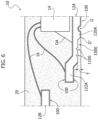
- Figure 6 illustrates embodiments of the present description wherein adhesion between metallic material of the die pad 12A and the molding compound 20 may be further facilitated at peripheral recessed portion 1000 of the die mounting portion by forming (via laser ablation LB) therein sculpturing 1100 - such as notches or trenches 1100 running along the recessed peripheral portion 1000.
- Figure 6 also illustrates that the peripheral recessed portion 1000 may be provided at the back/bottom surface of the die pad 12A in addition to (otherwise conventional) grooves G thus further reducing the risk of resin leaks undesirably covering the central portion of the second surface of the die pad 12A.
Landscapes
- Structures Or Materials For Encapsulating Or Coating Semiconductor Devices Or Solid State Devices (AREA)
- Engineering & Computer Science (AREA)
- Microelectronics & Electronic Packaging (AREA)
- Encapsulation Of And Coatings For Semiconductor Or Solid State Devices (AREA)
Abstract
Description
- The description relates to semiconductor devices.
- One or more embodiments can be applied to semiconductor devices including integrated circuits (ICs), for instance.
- Current manufacturing processes of (integrated circuit, IC) semiconductor devices comprise molding an insulating molding compound onto the devices to provide an insulating encapsulation thereto.
- Resin leaks or flashes at the bottom surface of the die pad that can undesirably result from the molding step and may cause inadequate plating of the bottom surface of the die pad.
- For instance, resin flashes have been observed to cause formation of so-called "tin islands" at the periphery of the bottom surface of the die pad; these lumps of solder material may detach from the die pad and possibly cause undesired short circuits between the leads.
- Resin flashes may be removed via de-flashing processes such as dry de-flashing via laser ablation, for instance, or chemical de-flashing.
- However, conventional de-flashing processes come with the drawback of undesirably promoting delamination between the metallic material (copper, for instance) of the leadframe and the electrically insulating encapsulation.
- Document
US 2007126092 A1 discloses a package to encase a semiconductor package that is manufactured by the following steps. First, an electrically conductive frame is provided. The frame has a plurality of leadframes arranged in a matrix with each leadframe having a plurality of spaced leads extending outwardly from a central aperture. The electrically conductive frame further includes a plurality of connecting bars joining outer end portions of adjacent ones of the leadframes. Second, a groove is formed in the connecting bars to form a reduced thickness portion between the outer end portions of adjacent ones of the leadframes. Third, a semiconductor device is electrically coupled to inner portions of said leads. Fourth, the frame and the semiconductor devices are encapsulated in a molding compound. Finally, the molding compound and the frame are cut along the grooves to form singulated semiconductor packages having outer lead portions with a height greater than the height of the reduced thickness portion. - Document
JP 2000260911 A - Document
JP 2004104155 A - Documents such as
JP 2012244038 A US 11264309 B2 US 2013075881 A1 ,US 20200273813 A1 ,US 20110266662 A1 ,JP 2017079229 A US 20220093494 A1 ,US 10366943 B2 US 10784186 B2 US 7262491 B2 andUS 20230187296 A1 provide background information in the related technological area. - An object of one or more embodiments is to overcome the drawbacks discussed in the foregoing.
- According to one or more embodiments, that object is achieved via a method having the features set forth in the claims that follow.
- One or more embodiments relate to a corresponding (integrated circuit) semiconductor device.
- The claims are an integral part of the technical teaching provided in respect of the embodiments.
- In solutions as described herein laser beam energy is applied to the bottom surface of a die pad to form therein a recessed portion that is subsequently filled with electrically insulating molding compound.
- In solutions as described herein, a roughened surface is formed at the recessed portion of the die pad that enhances adhesion between the molding compound and the die pad.
- In solutions as described herein, an adhesion promoter layer possibly provided at the bottom surface of the die pad is removed at the recessed portion thereof via laser ablation, prior to molding an electrically insulating encapsulation.
- Solutions as described herein may advantageously be applied to (integrated circuit) semiconductor devices provided with an exposed pad quad flat package (QFP), for instance.
- One or more embodiments will now be described, by way of example only, with reference to the annexed figures, wherein:
-
Figure 1 is a cross-sectional view of a semiconductor device to which embodiments of the present description can apply, -
Figure 2 is exemplary of a possible aspect of a portion of a back or bottom surface of a device as illustrated inFigure 1 , -
Figure 3 is an enlarged view corresponding to the portion ofFigure 2 indicated by the arrow III, -
Figure 4 is an enlarged view of the portion ofFigure 1 indicated by the arrow IV, -
Figures 5A and 5B are cross-sectional views of the same portion of a semiconductor device illustrative of processing steps according to embodiments of the present description, and -
Figure 6 is a cross-sectional view illustrative of possible embodiments of the present description. - Corresponding numerals and symbols in the different figures generally refer to corresponding parts unless otherwise indicated.
- The figures are drawn to clearly illustrate the relevant aspects of the embodiments and are not necessarily drawn to scale.
- The edges of features drawn in the figures do not necessarily indicate the termination of the extent of the feature.
- In the ensuing description one or more specific details are illustrated, aimed at providing an in-depth understanding of examples of embodiments of this description. The embodiments may be obtained without one or more of the specific details, or with other methods, components, materials, etc. In other cases, known structures, materials, or operations are not illustrated or described in detail so that certain aspects of embodiments will not be obscured.
- Reference to "an embodiment" or "one embodiment" in the framework of the present description is intended to indicate that a particular configuration, structure, or characteristic described in relation to the embodiment is comprised in at least one embodiment. Hence, phrases such as "in an embodiment" or "in one embodiment" that may be present in one or more points of the present description do not necessarily refer to one and the same embodiment.
- Moreover, particular conformations, structures, or characteristics may be combined in any adequate way in one or more embodiments.
- The headings/references used herein are provided merely for convenience and hence do not define the extent of protection or the scope of the embodiments.
- For simplicity and ease of explanation, throughout this description, and unless the context indicates otherwise, like parts or elements are indicated in the various figures with like reference signs, and a corresponding description will not be repeated for each and every figure.
-
Figure 1 is a cross-sectional view illustrative of an (integrated circuit, IC)semiconductor device 10 provided with a quad flat package (QFP). - The
exemplary device 10 illustrated inFigure 1 comprises: - a semiconductor die/chip 14 (the terms chip/s and die/dice are herein regarded as synonymous) attached at the top/front surface of a
die pad 12A in a leadframe, and - an array of
leads 12B arranged around the diepad 12A having the die 14 mounted thereon. - The designation "leadframe" (or "lead frame") is currently used (see, for instance the USPC Consolidated Glossary of the United States Patent and Trademark Office) to indicate a metal frame that provides support for an integrated circuit chip or die as well as electrical leads to interconnect the integrated circuit in the die or chip to other electrical components or contacts.
- Essentially, a leadframe comprises an array of electrically-conductive formations (or leads 12B) that from an outline location extend inwardly in the direction of a semiconductor chip or die 14 thus forming an array of electrically-conductive formations from a
die pad 12A configured to have at least one (integrated circuit - IC) semiconductor die attached thereon. This may be via conventional means such as a die attach adhesive (a die attach film, for instance, as illustrated inFigure 4 and referenced therein with the reference DA). - As exemplified in
Figure 1 , asemiconductor device 10 may be provided with adie pad 12A having a (central)die mounting region 120A and a raisedrim 122A around the die mounting region giving the diepad 12A a vat-like shape. - As illustrated herein by way of example, an (integrated circuit) semiconductor device such as the
device 10 may also comprise electrically conductive formations 16 (wires, for instance) that couple the semiconductor die 14 to the leads (outer pads) 12B (providing input/output signals, for instance) and/or to thedie pad 12A (providing a ground level, for instance) . - An electrically insulating molding compound 20 (an epoxy resin, for instance) is molded onto the assembly in order to provide the
semiconductor device 10 with a protective, electrically insulating encapsulation. - Manufacturing processes for obtaining a
semiconductor device 10 as illustrated inFigure 1 are conventional in the art which makes it unnecessary to provide a more detailed discussion herein. - A
semiconductor device 10 as illustrated inFigure 1 is configured to be mounted on a support such as a printed circuit board (PCB), for instance. To that effect, solder material (tin, for instance) may be provided at the bottom surface of thedie pad 12A. -
Figures 2 and 3 (whereinFigure 3 is an enlarged view of the portion ofFigure 2 indicated by the arrow III) illustrate the bottom surface of adie pad 12A of a (IC) semiconductor device such as thedevice 10 illustrated inFigure 1 . - As illustrated, a molding step as mentioned in the foregoing may undesirably result in some leaks of molding compound 20 (oftentimes referred to as molding/resin flashes) covering the bottom surface of the of the
die pad 12A, at the peripheral region thereof. - In order to counter the undesired resin flashes from covering a more extended portion of the bottom surface of the
die pad 12A, grooves G are provided at the bottom surface of thedie pad 12A. In the examples illustrated inFigures 2 and 3 two grooves G are provided as trenches running along the periphery of thedie mounting location 120A, close to its edge, to contain resin flashes. - Resin flashes may cause inadequate plating of solder material on the bottom surface of the
die pad 12A and, consequently, may give rise to issues related to mounting/soldering on the final substrate (a PCB, for instance). - Moreover, it is observed that resin flashes as illustrated, for instance, in
Figure 3 , may cause so-called "tin islands" (where the reference to tin is merely due to a commonly used solder material) to form. These are small amounts of soldering material that is plated in regions of the bottom surface of thedie pad 12A (at the periphery thereof, for instance) left uncovered by themolding compound 20 leaks; these "lumps" of soldering material are prone to detach from thedie pad 12A (during processing, for instance) possibly causing undesired short circuits between theleads 12B, for instance, thus causing failure of the device. - According to a conventional approach, issues related to such molding flashes may be countered via so-called de-flashing processes that involve removing resin flashes formed at the bottom surface of the
die pad 12A. However, de-flashing processes such as chemical or dry de-flashing processes may undesirably reduce adhesion of themolding compound 20 to the metallic (copper, for instance) leadframe possibly causing delamination of themolding compound 20. - Delamination of the
molding compound 20 from thedie pad 12A or lead 12B may cause humidity or contaminants to enter the package possibly reaching the semiconductor die 14 and causing failure of thedevice 10. - Moreover, delamination caused by chemical de-flashing may be more severe when adhesion promoters (such as non-etching adhesion promoters, NEAP) are used to enhance adhesion between the
molding compound 20 and theleadframe -
Figure 4 is an enlarged view of the portion ofFigure 1 indicated by the arrow IV that illustrates an adhesion promoter (NEAP, for instance)layer 100 provided at the interface between themolding compound 20 and theleadframe - The
adhesion promoter layer 100 may be at least partly dissolved whendevices 10 are processed in a de-flashing bath, possibly causing delamination issues. It is observed that delamination is more likely to start at a line D, that is the points at the interface between thedie pad 12A and themolding compound 20 that are exposed to a de-flashing bath. - According to another conventional approach, a dry de-flashing process can be used to remove molding compound flashes at the bottom surface of the
die pad 12A. - Dry de-flashing may involve applying laser beam energy to the bottom surface of the
die pad 12A to remove the undesired resin flashes via laser ablation. - However, in order to counter undesired ablation of molding compound of the package, laser ablation does not conventionally extend to the edge of the back/bottom surface of the
die pad 12A exposed at the bottom of thedevice 10. - In other words, laser beam energy is not applied to a "safety" zone S (of about 100 microns, for instance) at the periphery of the back/bottom surface of the
die pad 12A exposed at the bottom surface of the device 10 (on the right of the interface line D inFigure 4 ) in order not to undesirablyablate molding compound 20 forming the electrically insulating encapsulation (on the left of the interface line D inFigure 4 ). - Solutions as described herein involve applying laser beam energy to the bottom surface of a die pad to form therein a recessed portion that is subsequently filled with electrically insulating material during molding.
- In solutions as described herein, a roughened surface may be formed at the recessed portion of the die pad that enhances adhesion between the molding compound and the die pad.
- In solutions as described herein, an adhesion promoter layer possibly provided at the bottom surface of the die pad is removed at the recessed portion thereof via laser ablation, prior to molding an electrically insulating encapsulation.
- Solutions as described herein may advantageously be applied to (integrated circuit) semiconductor devices provided with an exposed pad quad flat package (QFP) as the
semiconductor device 10 illustrated inFigure 1 , for instance. -
Figures 5A and 5B are illustrative of processing steps according to embodiments of the present description applied to a semiconductor device such as thesemiconductor device 10 exemplified inFigure 1 . - As known to those skilled in the art, a plurality of semiconductor devices (such as the
semiconductor device 10 illustrated inFigure 1 ) can be concurrently processed by providing a common substrate (such as a leadframe reel or panel, for instance) comprising a plurality of individual substrates/leadframes. Individual leadframes may be held together via connecting bars (or dam bar) running around the periphery of each (individual) leadframe. A final singulation step removes the connecting bars (dam bars) to obtain a plurality of individual semiconductor devices. - For simplicity and ease of explanation, the following description will refer to manufacturing a single device.
- It will be appreciated that the details of the structure of a
device 10 as discussed herein are merely exemplary of a device where solutions as described herein may advantageously be applied, and shall not be construed in a limiting sense. - For instance, those skilled in the art may appreciate that solutions as described herein may be applied, for instance, also in case of other packages having an exposed die pad such as quad flat no leads packages (QFN) and/or to leadframes having no downset between the
die pad 12A and theleads 12B and/or to diepads 12A not having a raisedrim 122A. -
Figure 5A is illustrative of asemiconductor die 14 mounted (via die attach material DA, for instance) at the top/front surface of adie pad 12A, at adie mounting region 120A thereof. - As illustrated, laser beam energy LB is applied to the back/bottom surface of the
die pad 12A, at the periphery of the bottom surface of thedie pad 12A to form therein a recessedportion 1000. That is, metallic material (copper, for instance) of thedie pad 12A is removed from the back/bottom surface thereof via laser ablation to form a recessedportion 1000 along the periphery of the back/bottom surface of thedie pad 12A. - As illustrated, the recessed
peripheral portion 1000 surrounds a central portion of the back/bottom surface that is opposite of thedie mounting region 120A at the front/top surface of thedie pad 12A. - The recessed
peripheral portion 1000 of the back/bottom surface of thedie pad 12A may be formed with a depth, indicated with the reference T inFigure 5A , in the range of 25 to 35 microns, for instance. - In exemplary case illustrated in
Figure 5A , an adhesion promoter layer (a NEAP layer, for instance) is provided on the surface of the leadframe (that is, thedie pad 12A and theleads 12B), both at the top/front and back/bottom surfaces of the leadframe, as illustrated inFigure 5A . - As illustrated, applying laser beam energy LB to form the peripheral recessed
region 1000 of the back/bottom surface of thedie pad 12A results in theadhesion promoter layer 100 being removed (ablated) at the peripheral recessedregion 1000. - Said otherwise, the recessed peripheral portion of the second surface of the
die pad 12A is exempt from theadhesion promoter layer 100 in response to the laser beam energy LB applied thereto. -
Figure 5B is illustrative of a molding step where an electrically insulating encapsulation material 20 (such as an epoxy resin, for instance) is molded onto the substrate (a leadframe, for instance) 12A, 12B having asemiconductor die 14 mounted thereon, subsequently to forming the recessedportion 1000 as described in the foregoing. - As illustrated, the (electrically insulating)
molding compound 20 fills the recessedperipheral portion 1000 of the back/bottom surface of thedie pad 12A thus forming a layer (having a thickness notionally equal to the depth T of the recessed portion 1000) ofencapsulation material 20 that covers the back/bottom surface of thedie pad 12A at the recessedportion 1000. - Said otherwise, subsequently to the molding step, the bottom surface of a
device 10 comprises: - a central, inner region of the bottom surface of the
die pad 12A (inwardly of the border line D') where the metallic material of thedie pad 12A is not covered by theencapsulation material 20, and - a peripheral, outer region of the bottom surface of the
die pad 12A, that is, the peripheral recessedportion 1000, where the metallic material of thedie pad 12A is covered byencapsulation material 20. - As illustrated, in devices where the
die pad 12A comprises a raisedrim 122A around thedie mounting region 120A, theperipheral rim 122A is embedded in theencapsulation material 20. - It is observed that a peripheral recessed
region 1000 formed at thedie mounting region 120A counters undesired leakage of molding material over the central portion of the back/bottom surface of thedie pad 12A. - As mentioned, the recessed
peripheral portion 1000 of the back/bottom surface of thedie pad 12A may be formed with a depth, in the range of 25 to 35 microns, for instance. - Relatively shallow recessed
peripheral portions 1000, having a depth, for instance, between 2 and 3 microns, may also be formed that have been observed to give satisfactory results in terms of countering undesired leakage of molding material over the central portion of the back/bottom surface of thedie pad 12A. - It is noted that a de-flashing step (a per se conventional de-flashing step such as chemical de-flashing step, for instance) may be performed subsequent to the molding step.
- It is observed that such a de-flashing step does not completely remove the (electrically insulating)
molding compound 20 that fills the recessedperipheral portion 1000 also in embodiments where the layer ofencapsulation material 20 at the recessedportion 1000 has a thickness between 2 and 3 microns. Said otherwise, a de-flashing step leaves thedie pad 12A material (copper, for instance) at the recessedperipheral portion 1000 covered with a layer of encapsulation material 20 (possibly with a thickness between 2 and 3 microns) . - Moreover, applying laser beam energy LB to form a peripheral recessed
portion 1000 as illustrated in the figures, has the effect of roughening the back/bottom surface of thedie mounting region 120A at the peripheral recessedportion 1000. - As used herein, according to common usage, a surface being "roughened" indicates that such a surface is made rough.
- A rough surface has been found to promote adhesion between the
encapsulation material 20 and thedie pad 12A, thus reducing the risk of delamination. - In summary, solutions as described herein in relation to
Figures 5A, 5B and6 , involve molding anencapsulation 20 of electrically insulating material (an epoxy resin, for instance) onto a substrate (such as a leadframe comprisingdie pad 12A and leads 12B) having at (least one) semiconductor die 14 arranged thereon. - As illustrated in the figures, the semiconductor die 14 is arranged at a
die mounting region 120A at a first (top/front) surface of adie pad 12A in the substrate, wherein thedie pad 12A having a second (bottom/back) surface opposite the first surface. - Laser beam energy LB is applied to the second surface of the
die pad 12A to form therein a recessed peripheral portion 1000 (preferably, having a depth between 25 and 35 microns) surrounding a central portion opposite thedie mounting region 120A at the first surface. - During molding the electrically insulating
material 20 covers the recessedperipheral portion 1000 and leakage of the electrically insulatingmaterial 20 over said central portion is countered in response to theperipheral portion 1000 of the second surface of thedie pad 12A being recessed. - Advantageously, the recessed
peripheral portion 1000 of the second surface of thedie pad 12A is roughened in response to laser beam energy LB applied thereto, thus facilitating adhesion of the electrically insulatingmaterial 20 to the recessed peripheral portion. -
Figure 6 illustrates embodiments of the present description wherein adhesion between metallic material of thedie pad 12A and themolding compound 20 may be further facilitated at peripheral recessedportion 1000 of the die mounting portion by forming (via laser ablation LB) therein sculpturing 1100 - such as notches ortrenches 1100 running along the recessedperipheral portion 1000. -
Figure 6 also illustrates that the peripheral recessedportion 1000 may be provided at the back/bottom surface of thedie pad 12A in addition to (otherwise conventional) grooves G thus further reducing the risk of resin leaks undesirably covering the central portion of the second surface of thedie pad 12A. - Without prejudice to the underlying principles, the details and the embodiments may vary, even significantly, with respect to what has been described by way of example only without departing from the scope of the embodiments.
- The extent of protection is determined by the annexed claims.
Claims (12)
- A method, comprising:providing an adhesion promoter layer (100) on first and second opposite surfaces of a die pad (12A) in a substrate (12A, 12B),molding an encapsulation (20) of electrically insulating material onto the substrate (12A, 12B) having at least one semiconductor die (14) arranged thereon at a die mounting region (120A) of the first surface of the die pad (12A) in the substrate (12A, 12B),wherein the method comprises applying laser beam energy (LB) to the second surface of the die pad (12A) to form in the second surface of the die pad (12A) a recessed peripheral portion (1000) surrounding a central portion, said central portion of the second surface of the die pad (12A) being opposite the die mounting region (120A) at the first surface, wherein applying laser beam energy (LB) to form the recessed peripheral portion (1000) of the second surface of the die pad (12A) comprises removing said adhesion promoter layer (100) therefrom, and wherein during said molding the electrically insulating material (20) covers said recessed peripheral portion (1000) with leakage of the electrically insulating material (20) over said central portion being countered in response to the peripheral portion (1000) of the second surface of the die pad (12A) being recessed.
- The method of claim 1, wherein the recessed peripheral portion (1000) of the second surface of the die pad (12A) has a depth in the range 25 to 35 microns.
- The method of claim 1 or claim 2, wherein the recessed peripheral portion (1000) of the second surface of the die pad (12A) is roughened in response to laser beam energy (LB) applied thereto, wherein adhesion of the electrically insulating material (20) to said recessed peripheral portion (1000) is facilitated.
- The method of any of claims 1 to 3, wherein the die pad (12A) comprises a raised rim (122A) around the die mounting region (120A) at the first surface of the die pad (12A), wherein said raised rim (122A) is embedded in the electrically insulating material (20) during said molding.
- The method of any of the previous claims, comprising forming sculpturing (1100) at the recessed peripheral portion (1000) of the second surface of the die pad (12A), wherein adhesion of the electrically insulating material (20) to said recessed peripheral portion (1000) is facilitated by said sculpturing (1100).
- The method of any of the previous claims, comprising providing grooves (G) at the central portion of the second surface of the die pad (12A).
- A device (10), comprising:an adhesion promoter layer (100) provided on first and second opposite surfaces of a die pad (12A) in a substrate (12A, 12B),an encapsulation (20) of electrically insulating material molded onto the substrate (12A, 12B) having at least one semiconductor die (14) arranged thereon at a die mounting region (120A) of the first surface of the die pad (12A) in the substrate (12A, 12B), anda recessed peripheral portion (1000) formed via laser beam energy (LB) applied to the second surface of the die pad (12A), the recessed peripheral portion (1000) surrounding a central portion opposite the die mounting region (120A) at the first surface, wherein said recessed peripheral portion of the second surface of the die pad (12A) is exempt from the adhesion promoter layer (100) in response to the laser beam energy (LB) applied thereto,wherein the electrically insulating material (20) covers said recessed peripheral portion (1000) with leakage of the electrically insulating material (20) over said central portion countered in response to the peripheral portion of the second surface of the die pad (12A) being recessed.
- The device (10) of claim 7, wherein the recessed peripheral portion (1000) of the second surface of the die pad (12A) has a depth in the range 25 to 35 microns.
- The device (10) of claim 7 or claim 8, wherein the recessed peripheral portion (1000) of the second surface of the die pad (12A) is roughened, with the electrically insulating material (20) adhering to said roughened surface.
- The device (10) of any of claims 7 to 9, wherein the die pad (12A) comprises a raised rim (122A) around the die mounting region (120A) at the first surface of the die pad (12A), wherein said raised rim (122A) is embedded in the electrically insulating material (20).
- The device (10) of any of claims 7 to 10, comprising sculpturing (1100) formed at the recessed peripheral portion (1000) of the second surface of the die pad (12A).
- The device (10) of any of claims 7 to 11, comprising grooves (G) provided at the central portion of the second surface of the die pad (12A).
Applications Claiming Priority (1)
| Application Number | Priority Date | Filing Date | Title |
|---|---|---|---|
| IT102023000021597A IT202300021597A1 (en) | 2023-10-17 | 2023-10-17 | PROCEDURE FOR MANUFACTURING SEMICONDUCTOR DEVICES AND CORRESPONDING SEMICONDUCTOR DEVICE |
Publications (1)
| Publication Number | Publication Date |
|---|---|
| EP4542629A1 true EP4542629A1 (en) | 2025-04-23 |
Family
ID=89308012
Family Applications (1)
| Application Number | Title | Priority Date | Filing Date |
|---|---|---|---|
| EP24207010.0A Pending EP4542629A1 (en) | 2023-10-17 | 2024-10-16 | Method of manufacturing semiconductor devices and corresponding semiconductor device |
Country Status (4)
| Country | Link |
|---|---|
| US (1) | US20250125228A1 (en) |
| EP (1) | EP4542629A1 (en) |
| CN (2) | CN223712707U (en) |
| IT (1) | IT202300021597A1 (en) |
Citations (14)
| Publication number | Priority date | Publication date | Assignee | Title |
|---|---|---|---|---|
| JP2000260911A (en) | 1999-03-09 | 2000-09-22 | Nec Corp | Semiconductor resin sealed package and method of manufacturing the same |
| JP2004104155A (en) | 2003-12-26 | 2004-04-02 | Matsushita Electric Ind Co Ltd | Semiconductor device |
| US20070126092A1 (en) | 2005-12-02 | 2007-06-07 | Advanced Interconnect Technologies Limited, A Corporation Of The Republic Of Mauritius | Leadless semiconductor package and method of manufacture |
| US7262491B2 (en) | 2005-09-06 | 2007-08-28 | Advanced Interconnect Technologies Limited | Die pad for semiconductor packages and methods of making and using same |
| US20110266662A1 (en) | 2010-04-29 | 2011-11-03 | Kun Yuan Technology Co., Ltd. | Leadframe enhancing molding compound bondability and package structure thereof |
| JP2012244038A (en) | 2011-05-23 | 2012-12-10 | Panasonic Corp | Lead frame, semiconductor device having the lead frame, and manufacturing method therefor |
| US20130075881A1 (en) | 2011-09-23 | 2013-03-28 | Wan-Yu HUANG | Memory card package with a small substrate |
| JP2017079229A (en) | 2015-10-19 | 2017-04-27 | 株式会社デンソー | Semiconductor device and manufacturing method thereof |
| US10366943B2 (en) | 2017-09-16 | 2019-07-30 | Amkor Technology, Inc. | Packaged electronic device having stepped conductive structure and related methods |
| US20200273813A1 (en) | 2019-02-22 | 2020-08-27 | Infineon Technologies Ag | Semiconductor packages including roughening features |
| US10784186B2 (en) | 2018-05-29 | 2020-09-22 | Katoh Electric Co., Ltd. | Semiconductor module |
| US11264309B2 (en) | 2019-06-24 | 2022-03-01 | Mediatek Inc. | Multi-row QFN semiconductor package |
| US20220093494A1 (en) | 2020-09-18 | 2022-03-24 | Chang Wah Technology Co., Ltd. | Lead frame |
| US20230187296A1 (en) | 2021-12-10 | 2023-06-15 | Stmicroelectronics S.R.L. | Die attachment method for semiconductor devices and corresponding semiconductor device |
-
2023
- 2023-10-17 IT IT102023000021597A patent/IT202300021597A1/en unknown
-
2024
- 2024-10-09 US US18/910,661 patent/US20250125228A1/en active Pending
- 2024-10-16 EP EP24207010.0A patent/EP4542629A1/en active Pending
- 2024-10-17 CN CN202422517219.0U patent/CN223712707U/en active Active
- 2024-10-17 CN CN202411451193.2A patent/CN119852185A/en active Pending
Patent Citations (14)
| Publication number | Priority date | Publication date | Assignee | Title |
|---|---|---|---|---|
| JP2000260911A (en) | 1999-03-09 | 2000-09-22 | Nec Corp | Semiconductor resin sealed package and method of manufacturing the same |
| JP2004104155A (en) | 2003-12-26 | 2004-04-02 | Matsushita Electric Ind Co Ltd | Semiconductor device |
| US7262491B2 (en) | 2005-09-06 | 2007-08-28 | Advanced Interconnect Technologies Limited | Die pad for semiconductor packages and methods of making and using same |
| US20070126092A1 (en) | 2005-12-02 | 2007-06-07 | Advanced Interconnect Technologies Limited, A Corporation Of The Republic Of Mauritius | Leadless semiconductor package and method of manufacture |
| US20110266662A1 (en) | 2010-04-29 | 2011-11-03 | Kun Yuan Technology Co., Ltd. | Leadframe enhancing molding compound bondability and package structure thereof |
| JP2012244038A (en) | 2011-05-23 | 2012-12-10 | Panasonic Corp | Lead frame, semiconductor device having the lead frame, and manufacturing method therefor |
| US20130075881A1 (en) | 2011-09-23 | 2013-03-28 | Wan-Yu HUANG | Memory card package with a small substrate |
| JP2017079229A (en) | 2015-10-19 | 2017-04-27 | 株式会社デンソー | Semiconductor device and manufacturing method thereof |
| US10366943B2 (en) | 2017-09-16 | 2019-07-30 | Amkor Technology, Inc. | Packaged electronic device having stepped conductive structure and related methods |
| US10784186B2 (en) | 2018-05-29 | 2020-09-22 | Katoh Electric Co., Ltd. | Semiconductor module |
| US20200273813A1 (en) | 2019-02-22 | 2020-08-27 | Infineon Technologies Ag | Semiconductor packages including roughening features |
| US11264309B2 (en) | 2019-06-24 | 2022-03-01 | Mediatek Inc. | Multi-row QFN semiconductor package |
| US20220093494A1 (en) | 2020-09-18 | 2022-03-24 | Chang Wah Technology Co., Ltd. | Lead frame |
| US20230187296A1 (en) | 2021-12-10 | 2023-06-15 | Stmicroelectronics S.R.L. | Die attachment method for semiconductor devices and corresponding semiconductor device |
Also Published As
| Publication number | Publication date |
|---|---|
| US20250125228A1 (en) | 2025-04-17 |
| CN119852185A (en) | 2025-04-18 |
| CN223712707U (en) | 2025-12-23 |
| IT202300021597A1 (en) | 2025-04-17 |
Similar Documents
| Publication | Publication Date | Title |
|---|---|---|
| US7579674B2 (en) | Semiconductor package configuration with improved lead portion arrangement | |
| US6841414B1 (en) | Saw and etch singulation method for a chip package | |
| US5710064A (en) | Method for manufacturing a semiconductor package | |
| US6005286A (en) | Increasing the gap between a lead frame and a semiconductor die | |
| JP2016105503A (en) | Semiconductor device | |
| KR20030007040A (en) | A semiconductor device and method of manufacturing the same | |
| US20090065915A1 (en) | Singulated semiconductor package | |
| US10707154B2 (en) | Semiconductor device and method for manufacturing the same | |
| US11227820B2 (en) | Through hole side wettable flank | |
| US8835225B2 (en) | Method for fabricating quad flat non-leaded semiconductor package | |
| JP7494107B2 (en) | Lead frame, manufacturing method thereof and semiconductor device | |
| US9847283B1 (en) | Semiconductor device with wettable corner leads | |
| US10651109B2 (en) | Selective plating of semiconductor package leads | |
| US5606204A (en) | Resin-sealed semiconductor device | |
| CN220510008U (en) | Semiconductor device and electronic system | |
| EP4273907B1 (en) | Method of manufacturing semiconductor devices | |
| US20250125228A1 (en) | Method of manufacturing semiconductor devices and corresponding semiconductor device | |
| EP3693992B1 (en) | Surface mount semiconductor device and method of manufacture | |
| US20220359352A1 (en) | Electronic package with concave lead end faces | |
| US20250014982A1 (en) | Method of manufacturing semiconductor devices, corresponding pre-molded leadframe and semiconductor device | |
| KR100319400B1 (en) | Semiconductor Package and Manufacturing Method | |
| US20250210471A1 (en) | Semiconductor chip packaging defect free dimple process and device | |
| US20240332106A1 (en) | Semiconductor device, corresponding manufacturing method and substrate for use therein | |
| US20250372538A1 (en) | Method of manufacturing semiconductor devices and corresponding semiconductor device | |
| EP4657521A1 (en) | A method of fabricating a semiconductor integrated circuits package |
Legal Events
| Date | Code | Title | Description |
|---|---|---|---|
| PUAI | Public reference made under article 153(3) epc to a published international application that has entered the european phase |
Free format text: ORIGINAL CODE: 0009012 |
|
| STAA | Information on the status of an ep patent application or granted ep patent |
Free format text: STATUS: THE APPLICATION HAS BEEN PUBLISHED |
|
| AK | Designated contracting states |
Kind code of ref document: A1 Designated state(s): AL AT BE BG CH CY CZ DE DK EE ES FI FR GB GR HR HU IE IS IT LI LT LU LV MC ME MK MT NL NO PL PT RO RS SE SI SK SM TR |
|
| STAA | Information on the status of an ep patent application or granted ep patent |
Free format text: STATUS: REQUEST FOR EXAMINATION WAS MADE |
|
| 17P | Request for examination filed |
Effective date: 20250908 |
|
| REG | Reference to a national code |
Ref country code: DE Ref legal event code: R079 Free format text: PREVIOUS MAIN CLASS: H01L0021480000 Ipc: H10W0099000000 |
|
| GRAP | Despatch of communication of intention to grant a patent |
Free format text: ORIGINAL CODE: EPIDOSNIGR1 |
|
| STAA | Information on the status of an ep patent application or granted ep patent |
Free format text: STATUS: GRANT OF PATENT IS INTENDED |
|
| RIC1 | Information provided on ipc code assigned before grant |
Ipc: H10W 99/00 20260101AFI20260116BHEP Ipc: H10W 74/10 20260101ALI20260116BHEP Ipc: H10W 70/40 20260101ALI20260116BHEP |
|
| INTG | Intention to grant announced |
Effective date: 20260218 |
|
| RIN1 | Information on inventor provided before grant (corrected) |
Inventor name: CATALANO, GUENDALINA Inventor name: MELLINA GOTTARDO, ALESSANDRO Inventor name: ARRIGONI, ALBERTO |
|
| GRAS | Grant fee paid |
Free format text: ORIGINAL CODE: EPIDOSNIGR3 |
|
| GRAA | (expected) grant |
Free format text: ORIGINAL CODE: 0009210 |
|
| STAA | Information on the status of an ep patent application or granted ep patent |
Free format text: STATUS: THE PATENT HAS BEEN GRANTED |