EP4542240A1 - Configurable radio frequency system - Google Patents
Configurable radio frequency system Download PDFInfo
- Publication number
- EP4542240A1 EP4542240A1 EP23204523.7A EP23204523A EP4542240A1 EP 4542240 A1 EP4542240 A1 EP 4542240A1 EP 23204523 A EP23204523 A EP 23204523A EP 4542240 A1 EP4542240 A1 EP 4542240A1
- Authority
- EP
- European Patent Office
- Prior art keywords
- module
- configurable
- port
- ports
- modules
- Prior art date
- Legal status (The legal status is an assumption and is not a legal conclusion. Google has not performed a legal analysis and makes no representation as to the accuracy of the status listed.)
- Pending
Links
Images



Classifications
-
- G—PHYSICS
- G01—MEASURING; TESTING
- G01R—MEASURING ELECTRIC VARIABLES; MEASURING MAGNETIC VARIABLES
- G01R31/00—Arrangements for testing electric properties; Arrangements for locating electric faults; Arrangements for electrical testing characterised by what is being tested not provided for elsewhere
- G01R31/28—Testing of electronic circuits, e.g. by signal tracer
- G01R31/2832—Specific tests of electronic circuits not provided for elsewhere
- G01R31/2836—Fault-finding or characterising
- G01R31/2844—Fault-finding or characterising using test interfaces, e.g. adapters, test boxes, switches, PIN drivers
-
- G—PHYSICS
- G01—MEASURING; TESTING
- G01R—MEASURING ELECTRIC VARIABLES; MEASURING MAGNETIC VARIABLES
- G01R29/00—Arrangements for measuring or indicating electric quantities not covered by groups G01R19/00 - G01R27/00
- G01R29/08—Measuring electromagnetic field characteristics
- G01R29/0864—Measuring electromagnetic field characteristics characterised by constructional or functional features
- G01R29/0871—Complete apparatus or systems; circuits, e.g. receivers or amplifiers
-
- H—ELECTRICITY
- H04—ELECTRIC COMMUNICATION TECHNIQUE
- H04B—TRANSMISSION
- H04B1/00—Details of transmission systems, not covered by a single one of groups H04B3/00 - H04B13/00; Details of transmission systems not characterised by the medium used for transmission
- H04B1/38—Transceivers, i.e. devices in which transmitter and receiver form a structural unit and in which at least one part is used for functions of transmitting and receiving
- H04B1/40—Circuits
- H04B1/401—Circuits for selecting or indicating operating mode
-
- G—PHYSICS
- G01—MEASURING; TESTING
- G01R—MEASURING ELECTRIC VARIABLES; MEASURING MAGNETIC VARIABLES
- G01R29/00—Arrangements for measuring or indicating electric quantities not covered by groups G01R19/00 - G01R27/00
- G01R29/08—Measuring electromagnetic field characteristics
- G01R29/0807—Measuring electromagnetic field characteristics characterised by the application
- G01R29/0814—Field measurements related to measuring influence on or from apparatus, components or humans, e.g. in ESD, EMI, EMC, EMP testing, measuring radiation leakage; detecting presence of micro- or radiowave emitters; dosimetry; testing shielding; measurements related to lightning
-
- G—PHYSICS
- G01—MEASURING; TESTING
- G01R—MEASURING ELECTRIC VARIABLES; MEASURING MAGNETIC VARIABLES
- G01R29/00—Arrangements for measuring or indicating electric quantities not covered by groups G01R19/00 - G01R27/00
- G01R29/08—Measuring electromagnetic field characteristics
- G01R29/0864—Measuring electromagnetic field characteristics characterised by constructional or functional features
- G01R29/0878—Sensors; antennas; probes; detectors
-
- G—PHYSICS
- G01—MEASURING; TESTING
- G01R—MEASURING ELECTRIC VARIABLES; MEASURING MAGNETIC VARIABLES
- G01R31/00—Arrangements for testing electric properties; Arrangements for locating electric faults; Arrangements for electrical testing characterised by what is being tested not provided for elsewhere
- G01R31/28—Testing of electronic circuits, e.g. by signal tracer
- G01R31/2851—Testing of integrated circuits [IC]
- G01R31/2886—Features relating to contacting the IC under test, e.g. probe heads; chucks
- G01R31/2889—Interfaces, e.g. between probe and tester
-
- H—ELECTRICITY
- H04—ELECTRIC COMMUNICATION TECHNIQUE
- H04B—TRANSMISSION
- H04B17/00—Monitoring; Testing
- H04B17/0082—Monitoring; Testing using service channels; using auxiliary channels
- H04B17/0085—Monitoring; Testing using service channels; using auxiliary channels using test signal generators
-
- G—PHYSICS
- G01—MEASURING; TESTING
- G01R—MEASURING ELECTRIC VARIABLES; MEASURING MAGNETIC VARIABLES
- G01R27/00—Arrangements for measuring resistance, reactance, impedance, or electric characteristics derived therefrom
- G01R27/02—Measuring real or complex resistance, reactance, impedance, or other two-pole characteristics derived therefrom, e.g. time constant
- G01R27/04—Measuring real or complex resistance, reactance, impedance, or other two-pole characteristics derived therefrom, e.g. time constant in circuits having distributed constants, e.g. having very long conductors or involving high frequencies
-
- G—PHYSICS
- G01—MEASURING; TESTING
- G01R—MEASURING ELECTRIC VARIABLES; MEASURING MAGNETIC VARIABLES
- G01R27/00—Arrangements for measuring resistance, reactance, impedance, or electric characteristics derived therefrom
- G01R27/28—Measuring attenuation, gain, phase shift or derived characteristics of electric four pole networks, i.e. two-port networks; Measuring transient response
- G01R27/32—Measuring attenuation, gain, phase shift or derived characteristics of electric four pole networks, i.e. two-port networks; Measuring transient response in circuits having distributed constants, e.g. having very long conductors or involving high frequencies
-
- G—PHYSICS
- G01—MEASURING; TESTING
- G01R—MEASURING ELECTRIC VARIABLES; MEASURING MAGNETIC VARIABLES
- G01R31/00—Arrangements for testing electric properties; Arrangements for locating electric faults; Arrangements for electrical testing characterised by what is being tested not provided for elsewhere
- G01R31/28—Testing of electronic circuits, e.g. by signal tracer
- G01R31/282—Testing of electronic circuits specially adapted for particular applications not provided for elsewhere
- G01R31/2822—Testing of electronic circuits specially adapted for particular applications not provided for elsewhere of microwave or radiofrequency circuits
Definitions
- the invention relates to a configurable RF system, in particular a frontend system for a test and/or measurement device such as a spectrum analyzer or a signal generator.
- Test and/or measurement devices can be used for characterizing so called devices-under-test (DUTs).
- the DUTs can be waveguide modules or substrate-based circuits, e.g. MMICs (Monolithic Microwave Integrated Circuits), which operate with millimeter wave (mmW) signals.
- MMICs Monitoring Microwave Integrated Circuits
- mmW millimeter wave
- mmW converters e.g., mmW converters
- a network analyzer and two mmW converters may be used.
- an additional amplifier is connected to the setup, as the output power of the mmW converters may not be sufficient for many measurements. This can, however, reduce the directivity of the mmW converters, i.e. the DUT can no longer be characterized with respect to the input reflection coefficient.
- the source signal may no longer be measurable via the directional coupler. Thus, the amplifier is not used for all measurements.
- a network analyzer and two mmW converter or a spectrum analyzer, a mixer, and a noise source may be used; and for linearity measurements, a network analyzer and two or three mmW converters may be used.
- additional devices and frontends e.g., vector signal generators might be required.
- a measurement setup often has to be changed when performing new measurements. For instance, external frontends are swapped or additional devices are connected. This is cumbersome and time consuming. Further, a new calibration of the setup is often repeated every time the setup is changed, causing additional efforts.
- the invention relates to a configurable radio frequency (RF) system.
- the configurable RF system comprises: a first RF module, and a second RF module.
- Each of the first and the second RF module comprises: an RF circuitry; a signal path, in particular a waveguide; and an RF port connected to the respective signal path; wherein the RF port of the first RF module and the RF port of the second RF module are spaced apart at a predetermined distance and are oriented to enable a connection to a third RF module of the configurable RF system.
- the RF system can be a frontend system, which is connected between the test and/or measurement device (e.g., a network analyzer, a signal generator or a spectrum analyzer) and a device-under-test (DUT) and which can forward RF signals between these devices.
- the test and/or measurement device e.g., a network analyzer, a signal generator or a spectrum analyzer
- DUT device-under-test
- the configurable RF system provides a universal usability (i.e., it can be used with different test/measurement devices and for different measurements) and, thus, reduces the number of frontends required by a user. This also saves the time that is required for a conversion of a conventional measurement setup with different frontends.
- first RF module and the second RF module are screwed and/or clipped together.
- this connection is fixed and not releasable by a user or operator of the RF system.
- the RF port of the first and/or the second RF module comprises a waveguide flange or a coaxial interface.
- first and/or second RF module can be controlled, e.g. by the test and/or measurement device.
- a configuration of the first and/or second RF module can be changed in this way.
- the data interface is a USB interface.
- the first and/or the second RF module comprise a respective power supply interface.
- the third RF module comprises: two RF ports which are spaced apart at the predetermined distance and are designed for connecting to the RF ports of the first and the second RF module, and a further RF port which is arranged for being connected to a device-under-test, DUT.
- the third RF module may further comprise a signal path which is connected: to the two RF ports that are connectable to the first/second RF module, and to the further RF port.
- the respective RF ports of the first and second RF module can be connected to a DUT, e.g. a single DUT port, via the third RF module.
- a DUT e.g. a single DUT port
- different measurements can be carried out with the DUT suing the first and the second RF module, without having to change the setup (e.g., without having to disconnecting the first RF module and connecting the second RF module to the DUT).
- the third RF module comprises at least one of: a coupler, a combiner, a splitter, a switch, an impedance tuner, and/or a multiplexer.
- the RF circuitry of the first and/or the second RF module comprises at least one of: an RF amplifier, an RF mixer, an RF attenuator, an RF switch, an RF isolator, a combiner, a coupler, a doubler, a multiplier, a circulator, a phase shifter, and/or a delay line.
- the first and/or the second RF module may provide a plurality of different functionalities. For instance, different elements can be activated or switched into the respective signal path, e.g. based on a received control command.
- the first RF module is a receiver module or a transmitter module.
- the second RF module is a receiver module or a transmitter module.
- both the first and the second RF module are receiver modules.
- both the first and the second RF module are transmitter modules.
- the RF ports of the first and the second RF module are arranged at the predetermined distance to each other with a tolerance of 100 pm or less.
- the distance tolerance of the RF ports is 100 ⁇ m or less when the first RF module is attached to or fixated to the second RF module.
- the third RF module is detachably attached to the first and the second RF module.
- the RF system can be a modular system, which allow a user to connect different RF modules to the (interconnected) first and second RF module, depending on the requirements.
- the third RF module can be directly connected to the first and the second RF module without using cables. This is especially advantageous when using mmW signals that are transmitted via waveguides in the RF modules.
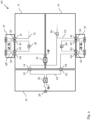
- Fig. 1 shows a schematic diagram of a configurable and/or modular RF system 10 according to an embodiment.
- the RF system 10 comprises: a first RF module 11; and a second RF module 21 which is attached to the first RF module 11.
- Each of the first and the second RF module 11, 21 comprises: an RF circuitry 12, 22, a signal path 13, 23, in particular a waveguide, and an RF port 14, 24 connected to the respective signal path 13, 23.
- the RF port 14 of the first RF module 11 and the RF port 24 of the second RF module 21 are spaced apart at a predetermined distance and oriented to enable a connection to a third RF module 31 of the configurable RF system 10.
- the configurable and/or modular RF system 10 can be a frontend system which is arranged between a test and/or measurement device 72 and a DUT 71.
- each of the first and the second RF module 11, 21 can comprise a dedicated RF port 17, 27 for connecting to a RF port of the test and/or measurement device.
- the RF system 10 can be configured to forward RF signals, in particular mmW signals, between the test and/or measurement device 72 and the DUT 71.
- the respective signal paths 13, 23 of the first and the second RF module 11, 21 can be designed as RF waveguides, in particular waveguides for mmW radiation.
- the RF waveguides can be rectangular metallic waveguides.
- Each of the RF ports 14, 24, 17, 27 of the first and/or the second RF module can be designed as or can comprise a waveguide flange. Alternatively, each of these interfaces can also be designed as or comprise coaxial interfaces.
- each of the first and/or the second RF module 11, 21 may comprise a respective data interface 15, 25.
- This data interface can be a USB interface.
- the RF modules 11, 21 can receive control commands via the data interface.
- an RF module 11, 21 can activate or switch an RF element (e.g., an amplifier, an attenuator, a filter etc.) into the signal path when receiving a respective control command.
- an RF element e.g., an amplifier, an attenuator, a filter etc.
- the RF modules 11, 21 can be configured or adapted for a specific measurement without having to manually change the measurement setup.
- the first and/or the second RF module 11, 21 may further each comprise a respective power supply interface 16, 26.
- the data interfaces 15, 25 and/or the power supply interfaces 16, 26 can be connected to the test and/or measurement device 72.
- the third RF module 31 may comprise a data interface and/or a power supply interface. For instance, via these interfaces, the third RF module 31 can receive electrical energy, e.g. from the first or second RF module 11, 21 or from the test and/or measurement device 72 and/or can supply energy to further RF modules.
- the RF circuitry 12, 22 of the first and/or the second RF module 11, 21 can be connected to the signal path 13, 23 of the respective module 11, 21 and may comprise one or more elements which are configured to adapt and/or condition RF signals that are transmitted via the signal path 13, 23.
- each of RF circuitries 12, 22 may comprises at least one of: an RF amplifier, an RF mixer, an RF attenuator, an RF switch, an RF isolator, a combiner, a coupler, a doubler, a multiplier, a circulator, a phase shifter, and/or a delay line.
- Each of the first and the second RF module 11, 21 can be either a receiver module (RX module) or a transmitter module (TX module).
- a receiver module comprises a receiver or receiver circuitry and is configured to receive an RF signal via the RF port
- a transmitter module comprises a transmitter or transmitter circuitry and is configured to transmit an RF signal via the RF port.
- the first RF module 11 is an RX module and the second RF module 21 is a TX module, or vice versa. In this way, a frontend with both RX and TX capabilities can be provided.
- both the first and the second RF module 11, 21 can be either Rx or Tx modules.
- the third RF module may further comprise at least one element 35 which connects to the three RF ports 32, 33, 36 via a signal path 34, in particular a waveguide (e.g., a rectangular metallic waveguide).
- a waveguide e.g., a rectangular metallic waveguide
- the third RF module 31, can be configured to switch the RF ports 14, 24 of the first and second RF module 11, 21 to a single further port 36, which can be connected to the DUT.
- the third RF module 31 can selectively switch its further RF port 36 (that can be connected to a DUT) to the Rx or the Tx module. In this way, a half-duplex system can be released. If the element 35 is instead a coupler, a combiner or a splitter, the system 10 can even form a full-duplex system.
- the third RF module 31 can generate a two-tone signal by combining respective RF signals received via the RF ports 32, 33.
- the third RF module 31 may comprise further functionality, such as a digital interface with characterization data stored in the module for signal correction, transmission or reflection measurements (as a function of frequency).
- the third RF module 31 may further comprise a digital data storage which is configured to store device data referring to the third RF module 31.
- the data storage can be coupled to the digital interface (e.g., a data interface) of the third RF module 31, wherein the digital interface is adapted to couple the third RF module 31 with an external communication partner (e.g., the test and/or measurement device).
- the device data stored in the digital data storage may comprise a unique identifier for the third RF module 31 and/or data characterizing the RF signal path 34 and the RF port(s) 32, 33, 36 of the third RF module 31.
- the digital data storage may further receive control data for controlling the third RF module 31 and/or updated device data via the digital interface.
- the updated device data can be store the updated device data.
- the third RF module 31 can be detachably attached to the first and the second RF module 11 21.
- the third RF module 31 can be attached to the first and the second RF module 11, 21 by means of a plug-in connection, a screw connection or a magnetic connection.
- this connection is established by screwing the respective waveguide flanges of the RF ports 14, 24 of the first and second RF module 11, 21 to the flanges of the complementary RF ports 32, 33 of the third RF module 31.
- the third RF module 31 can be removed from the first and the second RF module 11, 21 to use the first and second RF modules 11, 21 separately and/or to improve the performance of these modules 11, 21 (e.g., by reducing an attenuation of both modules). In this way, for example, a noise figure of an Rx module and an output power of a Tx module can be improved.
- the RF system 10 may comprise an external multiplexer module.
- This external multiplexer module can be used instead of or in addition to the third RF module 31 and can enable switching between a plurality of further RF ports of the third RF module 31, e.g. a number of input and output ports for connecting to one or more DUTs.
- These further RF ports can be bidirectional ports. For instance, multiple DUTs could be connected to the further RF ports, e.g. two or more antennas for OTA measurements with cross and co-polarization.
- the third RF module 31 may comprise an active or passive impedance tuner.
- the impedance tuner can allow a user to adapt an impedance value and to carry out impedance specific measurements. For instance, source and/or load pull measurements can be carried out in this way without having to connect additional external impedance tuners.
- the first and the second RF modules 11, 21 can be arranged at a well-defined distance and orientation to each other and can be attached to each other (e.g., screwed to each other) .
- the RF ports 14, 24 of the first and second RF module 11, 21 can be spaced apart at the predetermined distance and orientation with a high tolerance of 100 pm or less. This is high tolerance is especially important when the RF ports 14, 24 are waveguide-interfaces (e.g., waveguide flanges) which should be aligned as precisely as possible (i.e., without offset) to the complementary RF ports 32, 33 of the third RF module 31, when the third RF module 31 is attached to the first and the second RF module 11, 21.
- waveguide-interfaces e.g., waveguide flanges
- the alignment of the RF ports 14, 24 of the first and second RF module 11, 21 fulfills the requirements for the max. allowed misalignment according to IEEE Std 1785.2-2016.
- the first and the second RF module 11, 21 can thereby be firmly connected or even housed in the same housing (e.g., of a remote measurement head or module).
- Different third RF modules 31 (with different functionalities) can be removably attached to the thus combined first and second RF modules 11, 21, resulting in a modular frontend system.
- the RF ports 14, 24 e.g., Rx and Tx ports of the first and second RF module 11, 21 can be accessible to the user.
- Fig. 2 shows a schematic diagram of the configurable RF system 10 according to an embodiment.
- the system 10 shown in Fig. 2 can be identical to the system shown in Fig. 1 .
- the configurable RF system 10 shown in Fig. 2 comprises the first RF module 11 which comprises the signal path 13 and the RF port 14; wherein the RF port 14 can be arranged for being connected to a further RF module (e.g., the third RF module 31) or to the DUT.
- the first RF module 11 may further comprise at least a first and a second auxiliary port 41, 42 which are accessible from outside the first RF module 11; wherein the first and the second auxiliary port 41, 42 are arranged for being connected to each other via: a first bridging element 52 or a first extension module 51 of the configurable RF system 10.
- the signal path 13 may be connected to the RF port 14 and pass through the first auxiliary port 41, and may further pass through the first bridging element 52 or the first extension module 51.
- the signal path 13 can further pass through the second auxiliary port 42.
- the first RF module 11 may further comprise at least a third and a fourth auxiliary port 43, 44 which are also accessible from outside the first RF module 11. Also, this third and fourth auxiliary ports 43, 44 can be arranged for being connected to each other via: a second bridging element 43, or the first extension module 51, or a second extension module (not shown) of the configurable RF system. As shown in Fig. 2 , the signal path 13 of the first RF module 11 may pass through said third auxiliary port, and may further pass through the second bridging element 53 or the first extension module 51 or the (not shown) second extension module. Further, the signal path 13 may pass through the fourth auxiliary port 44.
- the auxiliary ports 41, 42, 43, 44 can form an interface of the first RF module for connecting the first extension module 51 and/or the bridging element(s) 52, 53. In this way, the signal path can be "guided” out of the RF module 11 and into the extension module 51, where additional signal processing or conditioning steps can be carried out.
- the system 10 shown in Fig. 2 further comprises the second RF module 21 which comprises a (further) signal path 23 and a (further) RF port 24 which is arranged for being connected to the further (i.e., third) RF module 31 or to the DUT.
- the second RF module 21 which comprises a (further) signal path 23 and a (further) RF port 24 which is arranged for being connected to the further (i.e., third) RF module 31 or to the DUT.
- the second RF module 21 may have a partially equivalent design to the first RF module 11, and may also comprise: at least a (further) first and a (further) second auxiliary port 41, 42 which are accessible from outside the second RF module 21, wherein the (further) first and the (further) second auxiliary port 41, 42 are arranged for being connected to each other via: a (third) bridging element 52 or a (third) extension module 51 of the configurable RF system 10.
- the further signal path 23 may be connected to the further RF port 24 of the second RF module 21 and pass through the (further) first auxiliary port 41, and further pass through the (third) bridging element 52 or the (third) extension module 51.
- the further signal path 23 may further pass through the further second auxiliary port 44.
- the second RF module 21 may comprise (further) third and fourth auxiliary ports 44, 43 which are accessible from outside the second RF module 21.
- the (further) third and fourth auxiliary ports 44, 43 can be arranged for being connected to each other via: a (fourth) bridging element 53, or the (third) extension module 51, or a fourth extension module (not shown).
- the further signal path 53 can pass through the further third auxiliary port 43, and can further pass through the fourth bridging element 53, or the third extension module 51 or the fourth extension module.
- the further signal path 23 can further pass through the further fourth auxiliary port 44.
- the respective signal path 13, 23 of the first and/or the second RF module 11, 21 can be RF signal paths.
- the respective signal paths 13, 23 are designed as RF waveguides, in particular waveguides for guiding mmW radiation.
- the RF waveguides can be rectangular metallic waveguides.
- Each of the RF ports and/or auxiliary ports 14, 24, 41, 42, 43, 44 of the first and/or the second RF module 11, 21 can be or can comprise waveguide flanges. Alternatively, each of these interfaces can also be coaxial interfaces.
- the first RF module 11 can be a transmitter (Tx) module and the second RF module 21 can be a receiver (Rx) module.
- both RF modules 11, 21 can be Rx or Tx modules.
- the first RF module 11 and the second RF module 21 can be arranged in a common housing or within separate housings.
- the first and the second RF module 11, 21 can be screwed and/or clipped together.
- the configurable RF system 10 comprises a data connection and/or a supply voltage connection which connects the first RF module 11 with the second RF module 21.
- a coupling element 19 can be arranged at an interface of the first and the second RF module 11, 21 and can be connected to the respective signal paths 13, 23 of the modules 11, 21. For instance, via this coupling element 19 at least a part of an RF signal can be coupled from a signal path of one RF module to the signal path of the other RF module.
- a Tx signal could be coupled from the Tx module (e.g., in Fig. 2 the first module 11) to the Rx module (e.g., in Fig. 2 the second module 21).
- a switch in the second module 21 can be arranged to selectively forward the thus received Tx signal portion or an Rx signal received via the RF port 24 to a connected test and/or measurement device.
- the coupled out signal part can be used as a reference receiver signal for a VNA (vector network analyzer) frontend or for analyzing the output signal of the Tx module (e.g., for digital pre-distortion of a modulated/broadband TX signal).
- VNA vector network analyzer
- this connection allows a combining of two signal sources for generating a two- or more-tone signal.
- the coupling element 19 can be a coupler, a combiner, a splitter or a switch.
- the coupling element 19 can be arranged in or at a connection surface of the first and the second RF module 11, 21.
- the respective signal paths 13, 23 of the first and/or the second RF module 11, 21 can be arranged such that at least a part of the signal path 13, 23 between the first and fourth auxiliary port 41, 44 loops through the first respectively second RF module 11, 21.
- an electronic device 18, 28, such as an amplifier unit or an attenuator unit, can be arranged in the first and/or second RF module, such that the part of the signal path 13, 23 (that loops through the RF module) passes through the electronic device 18, 28.
- an RF signal transmitted by or received by an RF module 11, 21 can be amplified or attenuated.
- the electronic device can be a component of the RF circuitry 12, 22.
- the first RF module 11 and/or the second RF module 21 may comprises a plurality of sub-modules.
- each sub-module comprises two of the auxiliary ports 41, 42, 43, 44.
- Each sub-module can have a separate housing.
- the extension modules 51 which can be connected to the first and/or second RF module 11, 21 via the auxiliary ports 41-44 expand the functionality of the RF modules 11, 21.
- each of the extension modules 51 may comprises at least one of the following elements: an amplifier stage, a switching unit configured to connect at least one of the auxiliary ports to another auxiliary port, an attenuator unit, a filter unit, a phase shifter, an isolator, a circulator, a power detector, a mixer, a signal and/or noise source, a modulator, a coupler unit, a splitter, and/or a combiner.
- bridging elements 52, 53 which can be bridge-like elements that directly connect two auxiliary ports, may be comprised by the extension modules (as shown in Fig. 2 ) .
- extension modules 51 connected to both RF modules 11, 21 in Fig. 2 are only an example.
- a plurality of different extension modules (as e.g. shown in Figs. 3A-D ), which offer different functionalities, can be provided and can be connected to the first and/or to the second RF module 11, 21, depending on the requirements.
- each of the extension modules 51 can be removably attached to the first respectively second RF module 11, 21, e.g. by means of a plug-in connection, a screw connection or a magnetic connection.
- the first extension module 51 is screwed to the first RF module 11; or the first extension module 51 and the first RF module 11 are magnetically forced together.
- the magnetic attachment may replace a screw connection and allows for an easy mounting / replacement of the extension module e51 without needing special tools.
- the (third) extension module 51 can be attached to the second RF module 21 in the same way.
- FIG. 1 For attaching the extension modules 51 to the first and/or the second RF module 11, 21 may comprise: a toggle press, a snap lock, a clamping device based on rotation, or a hand screw or knob.
- the first and/or second RF module 11, 21 comprises at least one auxiliary port 41-44 which is connected to the respective signal path 13, 23 of the module 11, 21.
- This auxiliary port can be used to couple additional RF signals into or out of the respective signal path 13, 23.
- the Tx module (e.g., first RF module 11 in Fig. 2 ) may comprise an internal switch which switches the RF port 14 between a port connected to a test and/or measurement device and one of the auxiliary ports 41-44 which receives the external signal.
- a noise source could be connected to this auxiliary port or to the extension module 51 connected to this auxiliary port.
- the TX module 11 can generate and/or forward CW (continuous wave) signals and/or broadband signals, e.g. for S-parameter, large signal or linearity measurements.
- the TX module 11 could provide a noise source which can be switched on the RF port 14.
- the Rx module (e.g., the second RF module 21 in Fig. 2 ) could comprise an additional switch which could switch an output port (connected to the test and/or measurement device) between the signal path 23 connected to the RF port 24 and an auxiliary port 41-44.
- an external power meter (for calibration) could be connected to this auxiliary port.
- first and/or second RF module 11, 21 comprise two or more auxiliary ports 41-44, as shown in Fig. 2 , different external modules 51 can be connected to the first and/or second RF module 11, 21 which expand the functionality of these RF module.
- the extension modules 51 can connect at least one of the following elements to a signal path of an RF module: an additional output amplifier to a TX signal path or an LNA (low noise amplifier) to an RX signal path, a mixer, a level detector, a switch, one or more attenuators, a filter, a coupler, a splitter, an isolator, a phase shifter, a circulator, a power detector, a modulator, a combiner, a load tuner, or a source tuner.
- an additional output amplifier to a TX signal path or an LNA (low noise amplifier) to an RX signal path a mixer, a level detector, a switch, one or more attenuators, a filter, a coupler, a splitter, an isolator, a phase shifter, a circulator, a power detector, a modulator, a combiner, a load tuner, or a source tuner.
- an RF module has four auxiliary ports 41-44 (as the modules 11, 21 shown in Fig. 2 ), a bypassing of an internal function block of the module (e.g., an external stage in a Tx module) via a selective connection of auxiliary ports with a bridging element is possible.
- Figs. 3A-D show schematic diagrams of different extension modules 51 according to an embodiment.
- each of the modules 51 shown in Figs. 3A-D can be connected to the auxiliary ports 41-44 of the first and/or the second RF module 11, 21 in Fig. 2 .
- the extension module 51 shown in Fig. 3A comprises four ports 56 which can connect to the four auxiliary ports 41-44 of the RF module(s) 11, 21.
- the extension module 51 further comprises electrical or mechanical controlled switches 55 which can either generate a respective bypass between the ports 56 connected to the first and second auxiliary port 41, 42, and/or between the ports 56 connected to the third and fourth auxiliary port 43, 44 of an RF module.
- the switches 55 can also connect respective external ports 54 to the first and fourth auxiliary port 41, 44.
- the external ports 54 could be connected to a further external module or to another element, such as a signal or a noise source.
- the extension module 51 in Fig. 3A can offer an electrical or mechanical controlled bypass for further external modules.
- the extension module 51 shown in Fig. 3B may also provide an electrical or mechanical controlled bypass for external sources (e.g., noise sources, signal sources).
- a switch 55 can switch between a connection between two ports 51 connected to the third and fourth auxiliary port 43, 44 and a connection of the fourth auxiliary port 44 with an external port 54.
- the external port 54 When connected to a Tx module, the external port 54 can be a feeding port configured to receive an RF signal; and the connected RF module 11 (e.g., a Tx module) can be configured to transmit the thus received RF signal to its RF port.
- the external port 54 when connected to an RX module, can be a receiving port configured to output an RF signal which is transmitted via the signal path of the Rx module.
- Fig. 3C shows an extension module 51 which is a high output power module.
- This module 51 comprises an amplifier unit 56 (e.g., comprising one or more amplifiers) which can be inserted and/or connected to the signal path of the RF module.
- the extension module 51 in Fig. 3C can be connected to a Tx module to increase an output level of a Tx signal.
- an extension module 51 could comprising an attenuator and/or an LNA, e.g. for connecting to an Rx module.
- the performance of the RX/Tx module can be enhanced without reducing its functionality.
- the RF module (s) 11, 21 do not have to be re-designed when a new DUT with higher performance requirements for the power output stage is measured.
- Fig. 3D shows an extensions module 51 which allows for switching between a connection to an electronic device 18, 28 (e.g., a power amplifier unit) of a connected RF module and a bridging element arranged for bypassing the electronic device 18, 28 by directly connecting the first and fourth auxiliary port 41, 44 of the RF module.
- an electronic device 18, 28 e.g., a power amplifier unit
- the extension modules 51 can for instance be used to improve the performance of a low noise amplifier, to bypass an LNA to increase an input level, or to connect an additional attenuator to reduce an input level.
- the extension modules can be used to bypass parts of the signal path (e.g., a power amplifier in TX or LNA in RX) .
- a single extension module 51 can offer several functionalities by being design as a turnover plate, which can be dismounted for "reconfiguration", rotated around its own axis and re-mounted on the RF module.
- the extension modules 51 connected to the first and second RF module 11, 21 in Fig. 2 are examples for extension modules with such turnover plate designs.
- the extension modules 51 connect respective bridging elements 52, 53 to the first and second auxiliary ports 41, 42 and to the third and fourth auxiliary ports 43, 44 of the RF modules 11, 21.
- the electronic device 18, 28 of each module is connected to the respective signal path 13, 28.
- a further bridging element 58 connects the respective first and the fourth auxiliary ports 41, 44.
- This further bridging 58 element forms a bypass element for bypassing the electronic device 18, 28 (i.e., the electronic device is not connected to the signal path 13, 28 over with the RF signal is forwarded) . In this way, the electronic device 18, 28 can be switched in or out of the signal path 13, 23.
- the extension modules 51 can be swapped during operation of the RF system 10.
- during operation means that the DUT does not have to be disconnected (i.e., from the third RF module 31) when swapping of the extension module(s) 51.
- the RF modules 11, 21 can be configured to automatically detect a connected extension module 51. During operation, new or other additional in the software of the RF modules 11, 21 or the test and/or measurement device can then be activated for adapting of the system 10 on-the-fly.
- Fig. 4 shows a schematic diagram of the configurable RF system 10 according to an embodiment.
- the RF system 10 is used as a frontend of a test and/or measurement device 72 (e.g., a signal source or signal analyzer) which is used to analyze a DUT on a wafer.
- the DUT can be an MMIC or thin fil circuit on the wafer 73 which can be placed on a chuck 74 of a wafer prober.
- the system shown in Fig. 4 comprises the first and second RF module that are connected to an RF port of the test and/or measurement device 72.
- An extension module 51 is connected to at least two auxiliary ports 41, 42 of the first RF module 11. Further both RF modules 11, 21 are connected to the third RF module 31 via their (main) RF ports 14, 24.
- the third RF module e.g., an external combiner module for combining RF modules 11 and 21
- third RF module 31 is electrically connected to the DUT via a tip of a wafer prober 75.
Landscapes
- Physics & Mathematics (AREA)
- General Physics & Mathematics (AREA)
- Electromagnetism (AREA)
- Engineering & Computer Science (AREA)
- General Engineering & Computer Science (AREA)
- Computer Networks & Wireless Communication (AREA)
- Signal Processing (AREA)
- Computer Hardware Design (AREA)
- Microelectronics & Electronic Packaging (AREA)
- Transmitters (AREA)
- Measurement Of Resistance Or Impedance (AREA)
Abstract
The invention relates to a configurable radio frequency, RF, system (10), which comprises a first RF module (11); and a second RF module (21). Each of the first and the second RF module (11, 21) comprises: an RF circuitry (12, 22), a signal path (13, 23), in particular a waveguide, and an RF port (14, 24) connected to the respective RF signal path; wherein the RF port (14) of the first RF module (11) and the RF port (24) of the second RF module (21) are spaced apart at a predetermined distance and are oriented to enable a connection to a third RF module (31) of the configurable RF system (10).
Description
- The invention relates to a configurable RF system, in particular a frontend system for a test and/or measurement device such as a spectrum analyzer or a signal generator.
- Test and/or measurement devices, such as spectrum or network analyzers, can be used for characterizing so called devices-under-test (DUTs). The DUTs can be waveguide modules or substrate-based circuits, e.g. MMICs (Monolithic Microwave Integrated Circuits), which operate with millimeter wave (mmW) signals. In case of an MMIC, various measurements are often carried out at different test points in the circuit.
- Depending on the type of the characterization measurement and the parameters to be measured, different measurement devices and frontends (e.g., mmW converters) are thereby used.
- For instance, in case of low or high signal S-parameter measurements or measurements of certain wave-parameters of an mmW DUT, a network analyzer and two mmW converters may be used. Often, an additional amplifier is connected to the setup, as the output power of the mmW converters may not be sufficient for many measurements. This can, however, reduce the directivity of the mmW converters, i.e. the DUT can no longer be characterized with respect to the input reflection coefficient. In addition, the source signal may no longer be measurable via the directional coupler. Thus, the amplifier is not used for all measurements.
- For noise measurements, in contrast, a network analyzer and two mmW converter or a spectrum analyzer, a mixer, and a noise source may be used; and for linearity measurements, a network analyzer and two or three mmW converters may be used. For measuring other parameters and signals (e.g., EVM, IQ charts, RF spectra, modulated signals, etc.), additional devices and frontends (e.g., vector signal generators) might be required.
- Thus, a measurement setup often has to be changed when performing new measurements. For instance, external frontends are swapped or additional devices are connected. This is cumbersome and time consuming. Further, a new calibration of the setup is often repeated every time the setup is changed, causing additional efforts.
- Thus, it is an objective to provide a configurable RF system which avoids the above mentioned disadvantages.
- The object of the present invention is achieved by the solution provided in the enclosed independent claims. Advantageous implementations of the present invention are further defined in the dependent claims.
- According to a first aspect, the invention relates to a configurable radio frequency (RF) system. The configurable RF system comprises: a first RF module, and a second RF module.
- Each of the first and the second RF module comprises: an RF circuitry; a signal path, in particular a waveguide; and an RF port connected to the respective signal path; wherein the RF port of the first RF module and the RF port of the second RF module are spaced apart at a predetermined distance and are oriented to enable a connection to a third RF module of the configurable RF system.
- This achieves the advantage that a configurable RF system is provided which can be used together with different test and/or measurement devices. The RF system can be a frontend system, which is connected between the test and/or measurement device (e.g., a network analyzer, a signal generator or a spectrum analyzer) and a device-under-test (DUT) and which can forward RF signals between these devices.
- In particular, the configurable RF system provides a universal usability (i.e., it can be used with different test/measurement devices and for different measurements) and, thus, reduces the number of frontends required by a user. This also saves the time that is required for a conversion of a conventional measurement setup with different frontends.
- The RF system can be suitable for RF signals in an mmW wavelength range (mmW signals). Thus, the configurable RF system can form an mmW frontend system.
- The signal path of the first and/or the second RF module can be an RF signal path. For example, each signal path is designed as an RF waveguide, in particular an RF waveguide for guiding mmW signals. The RF waveguides can be rectangular metallic waveguides.
- The second RF module can be attached to the first RF module. For instance, the first RF module and the second RF module are attached to each other on their respective side surfaces.
- For example, the first RF module and the second RF module are screwed and/or clipped together. Typically, this connection is fixed and not releasable by a user or operator of the RF system.
- For example, the first RF module and the second RF module can be arranged in a common housing or within separate housings. The housing(s) can be metal housing(s).
- In an embodiment, the RF port of the first and/or the second RF module comprises a waveguide flange or a coaxial interface.
- In an embodiment, the first and/or the second RF module comprise a respective data interface.
- This achieves the advantage that a function of the first and/or second RF module can be controlled, e.g. by the test and/or measurement device. In particular, a configuration of the first and/or second RF module can be changed in this way.
- For example, the data interface is a USB interface.
- In an embodiment, the first and/or the second RF module comprise a respective power supply interface.
- In an embodiment, the third RF module comprises: two RF ports which are spaced apart at the predetermined distance and are designed for connecting to the RF ports of the first and the second RF module, and a further RF port which is arranged for being connected to a device-under-test, DUT.
- The third RF module may further comprise a signal path which is connected: to the two RF ports that are connectable to the first/second RF module, and to the further RF port.
- This achieves the advantage that the respective RF ports of the first and second RF module can be connected to a DUT, e.g. a single DUT port, via the third RF module. Thus, different measurements can be carried out with the DUT suing the first and the second RF module, without having to change the setup (e.g., without having to disconnecting the first RF module and connecting the second RF module to the DUT).
- In an embodiment, the third RF module comprises at least one of: a coupler, a combiner, a splitter, a switch, an impedance tuner, and/or a multiplexer.
- For instance, the third RF module is a combiner module which can combined RF signals from the first and second RF module. This combiner module can give the configurable RF system a full duplex capability when connected between the DUT and the first and second RF module.
- In an embodiment, the RF circuitry of the first and/or the second RF module comprises at least one of: an RF amplifier, an RF mixer, an RF attenuator, an RF switch, an RF isolator, a combiner, a coupler, a doubler, a multiplier, a circulator, a phase shifter, and/or a delay line.
- This achieves the advantage that the first and/or the second RF module may provide a plurality of different functionalities. For instance, different elements can be activated or switched into the respective signal path, e.g. based on a received control command.
- In an embodiment, the first RF module is a receiver module or a transmitter module.
- In an embodiment, the second RF module is a receiver module or a transmitter module.
- In an embodiment, both the first and the second RF module are receiver modules.
- In an embodiment, both the first and the second RF module are transmitter modules.
- For instance, if an RF module is configured as a receiver module, it receives RF signals via its RF port (e.g., from a connected DUT via the third RF module) and forwards said RF signals to a test and/or measurement device. If an RF module is configured as a transmitter module, it may receive RF signals from the test and/or measurement device and forward said RF signals via the RF port to the third RF module (and a DUT) .
- In an embodiment, the RF ports of the first and the second RF module are arranged at the predetermined distance to each other with a tolerance of 100 pm or less.
- This achieves the advantage that the RF connections between the first/second RF module and the third RF module can comply with the high requirements regarding tolerance and fitting accuracy for waveguides and their interfaces.
- In particular, the distance tolerance of the RF ports is 100 µm or less when the first RF module is attached to or fixated to the second RF module.
- In an embedment, the third RF module is detachably attached to the first and the second RF module.
- This achieves the advantage that the RF system can be a modular system, which allow a user to connect different RF modules to the (interconnected) first and second RF module, depending on the requirements.
- Preferably, the third RF module can be directly connected to the first and the second RF module without using cables. This is especially advantageous when using mmW signals that are transmitted via waveguides in the RF modules.
- In an embodiment, the third RF module is attached to the first and the second RF module by means of a plug-in connection, a screw connection or a magnetic connection.
- The invention will be explained in the following together with the figures.
- Fig. 1
- shows a schematic diagram of a configurable RF system according to an embodiment;
- Fig. 2
- shows a schematic diagram of a configurable RF system according to an embodiment;
- Figs. 3A-D
- show schematic diagrams of different extension modules according to an embodiment; and
- Fig. 4
- shows a schematic diagram of a configurable RF system according to an embodiment.
-
Fig. 1 shows a schematic diagram of a configurable and/ormodular RF system 10 according to an embodiment. - The
RF system 10 comprises: afirst RF module 11; and asecond RF module 21 which is attached to thefirst RF module 11. Each of the first and thesecond RF module RF circuitry signal path RF port respective signal path RF port 14 of thefirst RF module 11 and theRF port 24 of thesecond RF module 21 are spaced apart at a predetermined distance and oriented to enable a connection to athird RF module 31 of theconfigurable RF system 10. - The configurable and/or
modular RF system 10 can be a frontend system which is arranged between a test and/ormeasurement device 72 and aDUT 71. In particular, each of the first and thesecond RF module dedicated RF port - The
RF system 10 can be configured to forward RF signals, in particular mmW signals, between the test and/ormeasurement device 72 and theDUT 71. - The
respective signal paths second RF module - Each of the
RF ports - Furthermore, each of the first and/or the
second RF module respective data interface - For instance, the
RF modules RF module RF modules - The first and/or the
second RF module power supply interface - The data interfaces 15, 25 and/or the power supply interfaces 16, 26 can be connected to the test and/or
measurement device 72. - Furthermore, also the
third RF module 31 may comprise a data interface and/or a power supply interface. For instance, via these interfaces, thethird RF module 31 can receive electrical energy, e.g. from the first orsecond RF module measurement device 72 and/or can supply energy to further RF modules. - The
RF circuitry second RF module signal path respective module signal path RF circuitries - Each of the first and the
second RF module - In an example, the
first RF module 11 is an RX module and thesecond RF module 21 is a TX module, or vice versa. In this way, a frontend with both RX and TX capabilities can be provided. - The test and/or
measurement device 72 can be a device which generates signals and forwards them to the RF system 10 (e.g., a signal generator or VNA) or a device which receives signals from the RF system (e.g., a spectrum or network analyzer). Aconfigurable RF system 10, which comprises an Rx and a Tx receiver, can be used as a frontend system for both of these types of devices. - For instance, the RF port of the TX module (which forms an output port) and the RF port of the RX module (which forms an input port) can be connected to the third RF module 31 (e.g., without opening the modules). The
third RF module 31 can then selectively connect any one of theseports DUT 71. - Alternatively, both the first and the
second RF module - The
third RF module 31 may comprise at least threeRF ports RF ports - In particular, the
third RF module 31 comprises twoRF ports RF ports second RF module further RF port 36 which is arranged for being connected to theDUT 71. - The third RF module may further comprise at least one
element 35 which connects to the threeRF ports signal path 34, in particular a waveguide (e.g., a rectangular metallic waveguide). - The at least one
element 35 can comprise a switch, for instance a mechanically or electrically controllable switch, a coupler, a combiner, a splitter, or a multiplexer. - The
third RF module 31, can be configured to switch theRF ports second RF module further port 36, which can be connected to the DUT. - For instance, if the first and the
second RF module third RF module 31 can selectively switch its further RF port 36 (that can be connected to a DUT) to the Rx or the Tx module. In this way, a half-duplex system can be released. If theelement 35 is instead a coupler, a combiner or a splitter, thesystem 10 can even form a full-duplex system. - If the first and the
second RF module third RF module 31 can generate a two-tone signal by combining respective RF signals received via theRF ports - The
third RF module 31 may comprise further functionality, such as a digital interface with characterization data stored in the module for signal correction, transmission or reflection measurements (as a function of frequency). - For instance, the
third RF module 31 may further comprise a digital data storage which is configured to store device data referring to thethird RF module 31. The data storage can be coupled to the digital interface (e.g., a data interface) of thethird RF module 31, wherein the digital interface is adapted to couple thethird RF module 31 with an external communication partner (e.g., the test and/or measurement device). For example, the device data stored in the digital data storage may comprise a unique identifier for thethird RF module 31 and/or data characterizing theRF signal path 34 and the RF port(s) 32, 33, 36 of thethird RF module 31. The digital data storage may further receive control data for controlling thethird RF module 31 and/or updated device data via the digital interface. The updated device data can be store the updated device data. - The
third RF module 31 can be detachably attached to the first and thesecond RF module 11 21. For example, thethird RF module 31 can be attached to the first and thesecond RF module - In an example, this connection is established by screwing the respective waveguide flanges of the
RF ports second RF module complementary RF ports third RF module 31. - In addition, the
third RF module 31 can be removed from the first and thesecond RF module second RF modules modules 11, 21 (e.g., by reducing an attenuation of both modules). In this way, for example, a noise figure of an Rx module and an output power of a Tx module can be improved. - Furthermore, the
RF system 10 may comprise an external multiplexer module. This external multiplexer module can be used instead of or in addition to thethird RF module 31 and can enable switching between a plurality of further RF ports of thethird RF module 31, e.g. a number of input and output ports for connecting to one or more DUTs. These further RF ports can be bidirectional ports. For instance, multiple DUTs could be connected to the further RF ports, e.g. two or more antennas for OTA measurements with cross and co-polarization. - For example, the
third RF module 31 may comprise an active or passive impedance tuner. The impedance tuner can allow a user to adapt an impedance value and to carry out impedance specific measurements. For instance, source and/or load pull measurements can be carried out in this way without having to connect additional external impedance tuners. - The first and the
second RF modules RF ports second RF module RF ports complementary RF ports third RF module 31, when thethird RF module 31 is attached to the first and thesecond RF module - For instance, the alignment of the
RF ports second RF module - The first and the
second RF module second RF modules RF ports 14, 24 (e.g., Rx and Tx ports) of the first andsecond RF module -
Fig. 2 shows a schematic diagram of theconfigurable RF system 10 according to an embodiment. Thesystem 10 shown inFig. 2 can be identical to the system shown inFig. 1 . - The
configurable RF system 10 shown inFig. 2 comprises thefirst RF module 11 which comprises thesignal path 13 and theRF port 14; wherein theRF port 14 can be arranged for being connected to a further RF module (e.g., the third RF module 31) or to the DUT. Thefirst RF module 11 may further comprise at least a first and a secondauxiliary port first RF module 11; wherein the first and the secondauxiliary port first bridging element 52 or afirst extension module 51 of theconfigurable RF system 10. Thesignal path 13 may be connected to theRF port 14 and pass through the firstauxiliary port 41, and may further pass through thefirst bridging element 52 or thefirst extension module 51. Thesignal path 13 can further pass through the secondauxiliary port 42. - As shown in
Fig. 2 , thefirst RF module 11 may further comprise at least a third and a fourthauxiliary port first RF module 11. Also, this third and fourthauxiliary ports second bridging element 43, or thefirst extension module 51, or a second extension module (not shown) of the configurable RF system. As shown inFig. 2 , thesignal path 13 of thefirst RF module 11 may pass through said third auxiliary port, and may further pass through thesecond bridging element 53 or thefirst extension module 51 or the (not shown) second extension module. Further, thesignal path 13 may pass through the fourthauxiliary port 44. - The
auxiliary ports first extension module 51 and/or the bridging element(s) 52, 53. In this way, the signal path can be "guided" out of theRF module 11 and into theextension module 51, where additional signal processing or conditioning steps can be carried out. - The
system 10 shown inFig. 2 , further comprises thesecond RF module 21 which comprises a (further)signal path 23 and a (further)RF port 24 which is arranged for being connected to the further (i.e., third)RF module 31 or to the DUT. - The
second RF module 21 may have a partially equivalent design to thefirst RF module 11, and may also comprise: at least a (further) first and a (further) secondauxiliary port second RF module 21, wherein the (further) first and the (further) secondauxiliary port element 52 or a (third)extension module 51 of theconfigurable RF system 10. Thefurther signal path 23 may be connected to thefurther RF port 24 of thesecond RF module 21 and pass through the (further) firstauxiliary port 41, and further pass through the (third) bridgingelement 52 or the (third)extension module 51. Thefurther signal path 23 may further pass through the further secondauxiliary port 44. - Similar to the
first RF module 11, also thesecond RF module 21 may comprise (further) third and fourthauxiliary ports second RF module 21. The (further) third and fourthauxiliary ports element 53, or the (third)extension module 51, or a fourth extension module (not shown). Thefurther signal path 53 can pass through the further thirdauxiliary port 43, and can further pass through thefourth bridging element 53, or thethird extension module 51 or the fourth extension module. Thefurther signal path 23 can further pass through the further fourthauxiliary port 44. - The
respective signal path second RF module respective signal paths - Each of the RF ports and/or
auxiliary ports second RF module - For example, the
first RF module 11 can be a transmitter (Tx) module and thesecond RF module 21 can be a receiver (Rx) module. Alternatively, also bothRF modules - The
first RF module 11 and thesecond RF module 21 can be arranged in a common housing or within separate housings. - For instance, the first and the
second RF module configurable RF system 10 comprises a data connection and/or a supply voltage connection which connects thefirst RF module 11 with thesecond RF module 21. - Furthermore, a
coupling element 19 can be arranged at an interface of the first and thesecond RF module respective signal paths modules coupling element 19 at least a part of an RF signal can be coupled from a signal path of one RF module to the signal path of the other RF module. - For instance, in this way a Tx signal could be coupled from the Tx module (e.g., in
Fig. 2 the first module 11) to the Rx module (e.g., inFig. 2 the second module 21). A switch in thesecond module 21 can be arranged to selectively forward the thus received Tx signal portion or an Rx signal received via theRF port 24 to a connected test and/or measurement device. - For instance, in an Rx / Tx arrangement, the coupled out signal part can be used as a reference receiver signal for a VNA (vector network analyzer) frontend or for analyzing the output signal of the Tx module (e.g., for digital pre-distortion of a modulated/broadband TX signal). In a Tx / Tx arrangement, this connection allows a combining of two signal sources for generating a two- or more-tone signal.
- The
coupling element 19 can be a coupler, a combiner, a splitter or a switch. Thecoupling element 19 can be arranged in or at a connection surface of the first and thesecond RF module - As shown in
Fig. 2 , therespective signal paths second RF module signal path auxiliary port second RF module - For instance, an
electronic device signal path 13, 23 (that loops through the RF module) passes through theelectronic device RF module RF circuitry - The
first RF module 11 and/or thesecond RF module 21 may comprises a plurality of sub-modules. For example, each sub-module comprises two of theauxiliary ports - Preferably, the
extension modules 51, which can be connected to the first and/orsecond RF module RF modules - For instance, each of the
extension modules 51 may comprises at least one of the following elements: an amplifier stage, a switching unit configured to connect at least one of the auxiliary ports to another auxiliary port, an attenuator unit, a filter unit, a phase shifter, an isolator, a circulator, a power detector, a mixer, a signal and/or noise source, a modulator, a coupler unit, a splitter, and/or a combiner. - Furthermore, the bridging
elements Fig. 2 ) . - In this way, a user or operator can easily adapt and/or configure the
RF system 10 by connecting asuitable extension module 51 to any one of theRF modules different extension modules 51 can be connected to the first and thesecond RF module 21 depending on the measurement requirements. Thus, theRF system 10 can be modular system that can be quickly adapted by connectingsuitable extension modules 51. - Note that the
extension modules 51 connected to bothRF modules Fig. 2 are only an example. A plurality of different extension modules (as e.g. shown inFigs. 3A-D ), which offer different functionalities, can be provided and can be connected to the first and/or to thesecond RF module - Thereby, each of the
extension modules 51 can be removably attached to the first respectivelysecond RF module - For example, the
first extension module 51 is screwed to thefirst RF module 11; or thefirst extension module 51 and thefirst RF module 11 are magnetically forced together. The magnetic attachment may replace a screw connection and allows for an easy mounting / replacement of the extension module e51 without needing special tools. The (third)extension module 51 can be attached to thesecond RF module 21 in the same way. - Further implementation examples/approaches for attaching the
extension modules 51 to the first and/or thesecond RF module - In general, the first and/or
second RF module respective signal path module respective signal path - For example, the Tx module (e.g.,
first RF module 11 inFig. 2 ) may comprise an internal switch which switches theRF port 14 between a port connected to a test and/or measurement device and one of the auxiliary ports 41-44 which receives the external signal. For example, a noise source could be connected to this auxiliary port or to theextension module 51 connected to this auxiliary port. This enables, for example, a comprehensive characterization of the DUT (e.g., chips/MMICs on a wafer prober system) without disconnecting the DUT and/or without modifying the measurement setup. For instance, theTX module 11 can generate and/or forward CW (continuous wave) signals and/or broadband signals, e.g. for S-parameter, large signal or linearity measurements. Furthermore, theTX module 11 could provide a noise source which can be switched on theRF port 14. - The Rx module (e.g., the
second RF module 21 inFig. 2 ) could comprise an additional switch which could switch an output port (connected to the test and/or measurement device) between thesignal path 23 connected to theRF port 24 and an auxiliary port 41-44. For instance, an external power meter (for calibration) could be connected to this auxiliary port. - In case the first and/or
second RF module Fig. 2 , differentexternal modules 51 can be connected to the first and/orsecond RF module - For instance, the
extension modules 51 can connect at least one of the following elements to a signal path of an RF module: an additional output amplifier to a TX signal path or an LNA (low noise amplifier) to an RX signal path, a mixer, a level detector, a switch, one or more attenuators, a filter, a coupler, a splitter, an isolator, a phase shifter, a circulator, a power detector, a modulator, a combiner, a load tuner, or a source tuner. In this way, a functionality and/or performance of anRF module - If an RF module has four auxiliary ports 41-44 (as the
modules Fig. 2 ), a bypassing of an internal function block of the module (e.g., an external stage in a Tx module) via a selective connection of auxiliary ports with a bridging element is possible. -
Figs. 3A-D show schematic diagrams ofdifferent extension modules 51 according to an embodiment. For instance, each of themodules 51 shown inFigs. 3A-D can be connected to the auxiliary ports 41-44 of the first and/or thesecond RF module Fig. 2 . - For instance, the
extension module 51 shown inFig. 3A comprises fourports 56 which can connect to the four auxiliary ports 41-44 of the RF module(s) 11, 21. Theextension module 51 further comprises electrical or mechanical controlledswitches 55 which can either generate a respective bypass between theports 56 connected to the first and secondauxiliary port ports 56 connected to the third and fourthauxiliary port switches 55 can also connect respectiveexternal ports 54 to the first and fourthauxiliary port external ports 54 could be connected to a further external module or to another element, such as a signal or a noise source. Thus, theextension module 51 inFig. 3A can offer an electrical or mechanical controlled bypass for further external modules. - The
extension module 51 shown inFig. 3B , may also provide an electrical or mechanical controlled bypass for external sources (e.g., noise sources, signal sources). Thereby, aswitch 55 can switch between a connection between twoports 51 connected to the third and fourthauxiliary port auxiliary port 44 with anexternal port 54. - When connected to a Tx module, the
external port 54 can be a feeding port configured to receive an RF signal; and the connected RF module 11 (e.g., a Tx module) can be configured to transmit the thus received RF signal to its RF port. Alternatively, when connected to an RX module, theexternal port 54 can be a receiving port configured to output an RF signal which is transmitted via the signal path of the Rx module. -
Fig. 3C shows anextension module 51 which is a high output power module. Thismodule 51 comprises an amplifier unit 56 (e.g., comprising one or more amplifiers) which can be inserted and/or connected to the signal path of the RF module. For instance, theextension module 51 inFig. 3C can be connected to a Tx module to increase an output level of a Tx signal. - Alternatively, an
extension module 51 could comprising an attenuator and/or an LNA, e.g. for connecting to an Rx module. - For instance, by connecting such an
extension module 51 to an Rx or Tx module, the performance of the RX/Tx module can be enhanced without reducing its functionality. Thus, the RF module (s) 11, 21 do not have to be re-designed when a new DUT with higher performance requirements for the power output stage is measured. -
Fig. 3D shows anextensions module 51 which allows for switching between a connection to anelectronic device 18, 28 (e.g., a power amplifier unit) of a connected RF module and a bridging element arranged for bypassing theelectronic device auxiliary port - When connected to an RX module, the
extension modules 51 can for instance be used to improve the performance of a low noise amplifier, to bypass an LNA to increase an input level, or to connect an additional attenuator to reduce an input level. - In case of an RF module with a plurality of auxiliary ports 41-44, preferably four auxiliary ports, which are connected to a signal path, the extension modules can be used to bypass parts of the signal path (e.g., a power amplifier in TX or LNA in RX) .
- Furthermore, a
single extension module 51 can offer several functionalities by being design as a turnover plate, which can be dismounted for "reconfiguration", rotated around its own axis and re-mounted on the RF module. - The
extension modules 51 connected to the first andsecond RF module Fig. 2 are examples for extension modules with such turnover plate designs. For instance, in the currently mounted configuration, theextension modules 51 connectrespective bridging elements auxiliary ports auxiliary ports RF modules electronic device respective signal path - However, when turning around and mounting the
extension modules 51 via its RF ports on the opposite side, a further bridgingelement 58 connects the respective first and the fourthauxiliary ports electronic device 18, 28 (i.e., the electronic device is not connected to thesignal path electronic device signal path - When using more complex modules on the additional auxiliary ports 41-44, an electrically controllable switching is also possible.
- Preferably, the
extension modules 51 can be swapped during operation of theRF system 10. Hereby, during operation means that the DUT does not have to be disconnected (i.e., from the third RF module 31) when swapping of the extension module(s) 51. - Furthermore, the
RF modules connected extension module 51. During operation, new or other additional in the software of theRF modules system 10 on-the-fly. -
Fig. 4 shows a schematic diagram of theconfigurable RF system 10 according to an embodiment. Thereby, theRF system 10 is used as a frontend of a test and/or measurement device 72 (e.g., a signal source or signal analyzer) which is used to analyze a DUT on a wafer. The DUT can be an MMIC or thin fil circuit on thewafer 73 which can be placed on achuck 74 of a wafer prober. - The system shown in
Fig. 4 comprises the first and second RF module that are connected to an RF port of the test and/ormeasurement device 72. - An
extension module 51 is connected to at least twoauxiliary ports first RF module 11. Further bothRF modules third RF module 31 via their (main)RF ports RF modules 11 and 21) is in turn connected to the DUT. For instance,third RF module 31 is electrically connected to the DUT via a tip of awafer prober 75. - All features described above or features shown in the figures can be combined with each other in any advantageous manner within the scope of the invention.
Claims (14)
- A configurable radio frequency, RF, system (10), comprising:a first RF module (11); anda second RF module (21);wherein each of the first and the second RF module (11, 21) comprises:- an RF circuitry (12, 22),- a signal path (13, 23), in particular a waveguide, and- an RF port (14, 24) connected to the respective signal path (13, 23);wherein the RF port (14) of the first RF module (11) and the RF port (24) of the second RF module (21) are spaced apart at a predetermined distance and are oriented to enable a connection to a third RF module (31) of the configurable RF system (10).
- The configurable RF system (10) of claim 1,
wherein the respective RF port (14, 24) of the first and/or the second RF module (11, 21) comprises a waveguide flange or a coaxial interface. - The configurable RF system (10)of claim 1 or 2,
wherein the first and/or the second RF module (11, 21) comprise a respective data interface (15, 25). - The configurable RF system (10) of any one of the preceding claims,
wherein the first and/or the second RF module (11, 21) comprise a respective power supply interface (16, 26). - The configurable RF system (10) of any one of the preceding claims,
wherein the third RF module (31) comprises:- two RF ports (32, 33) which are spaced apart at the predetermined distance and are designed for connecting to the RF ports (14, 24) of the first and the second RF module (21), and- a further RF port (36) which is arranged for being connected to a device-under-test, DUT (71). - The configurable RF system (10) of any one of the preceding claims,
wherein the third RF module (31) comprises at least one of: a coupler, a combiner, a splitter, a switch, an impedance tuner, and/or a multiplexer. - The configurable RF system (10) of any one of the preceding claims,
wherein the respective RF circuitry (12, 22) of the first and/or the second RF module (11, 21) comprises at least one of: an RF amplifier, an RF mixer, an RF attenuator, an RF switch, an RF isolator, a combiner, a coupler, a doubler, a multiplier, a circulator, a phase shifter, and/or a delay line. - The configurable RF system (10) of any one of the preceding claims,
wherein the first RF module (11) is a receiver module or a transmitter module. - The configurable RF system (10) of any one of the preceding claims,
wherein the second RF module (21) is a receiver module or a transmitter module. - The configurable RF system (10) of any one of the preceding claims,
wherein both the first and the second RF module (11, 21) are receiver modules. - The configurable RF system (10) of any one of claims 1 to 9,
wherein both the first and the second RF module (11, 21) are transmitter modules. - The configurable RF system (10) of any one of the preceding claims,
wherein the RF ports (14, 24) of the first and the second RF module (11, 21) are arranged at the predetermined distance to each other with a tolerance of 100 µm or less. - The configurable RF system (10) of any one of the preceding claims,
wherein the third RF module (31) is detachably attached to the first and the second RF module (11, 21). - The configurable RF system (10) of any one of the preceding claims,
wherein the third RF module (31) is attached to the first and the second RF module (11, 21) by means of a plug-in connection, a screw connection or a magnetic connection.
Priority Applications (3)
| Application Number | Priority Date | Filing Date | Title |
|---|---|---|---|
| EP23204523.7A EP4542240A1 (en) | 2023-10-19 | 2023-10-19 | Configurable radio frequency system |
| US18/739,415 US12607660B2 (en) | 2023-10-19 | 2024-06-11 | Configurable radio frequency system |
| CN202410949917.XA CN119865202A (en) | 2023-10-19 | 2024-07-16 | Configurable radio frequency system |
Applications Claiming Priority (1)
| Application Number | Priority Date | Filing Date | Title |
|---|---|---|---|
| EP23204523.7A EP4542240A1 (en) | 2023-10-19 | 2023-10-19 | Configurable radio frequency system |
Publications (1)
| Publication Number | Publication Date |
|---|---|
| EP4542240A1 true EP4542240A1 (en) | 2025-04-23 |
Family
ID=88504946
Family Applications (1)
| Application Number | Title | Priority Date | Filing Date |
|---|---|---|---|
| EP23204523.7A Pending EP4542240A1 (en) | 2023-10-19 | 2023-10-19 | Configurable radio frequency system |
Country Status (3)
| Country | Link |
|---|---|
| US (1) | US12607660B2 (en) |
| EP (1) | EP4542240A1 (en) |
| CN (1) | CN119865202A (en) |
Citations (8)
| Publication number | Priority date | Publication date | Assignee | Title |
|---|---|---|---|---|
| US20040010384A1 (en) * | 2002-07-12 | 2004-01-15 | Jacobsen Robert E. | System and method for measuring essential power amplification functions |
| US20040201383A1 (en) * | 2003-04-11 | 2004-10-14 | Anderson Keith F. | Balanced device characterization including test system calibration |
| GB2409049A (en) * | 2003-12-11 | 2005-06-15 | Agilent Technologies Inc | Measuring complex reflection coefficient of an RF source |
| CN103592547A (en) * | 2013-11-22 | 2014-02-19 | 中国电子科技集团公司第四十一研究所 | Wideband vector network analyzer |
| US20160204881A1 (en) * | 2011-06-13 | 2016-07-14 | Mediatek Inc. | Rf testing system using integrated circuit |
| US20160259700A1 (en) * | 2015-03-02 | 2016-09-08 | Rohde & Schwarz Gmbh & Co. Kg | Testing front end module, testing methods and modular testing systems for testing electronic equipment |
| CN205992026U (en) * | 2016-08-31 | 2017-03-01 | 福建星海通信科技有限公司 | A kind of port expansion device of vector network analyzer |
| US20190219612A1 (en) * | 2018-01-12 | 2019-07-18 | Rohde & Schwarz Gmbh & Co. Kg | Radio frequency measuring device module and radio frequency measuring device |
Family Cites Families (2)
| Publication number | Priority date | Publication date | Assignee | Title |
|---|---|---|---|---|
| US7640477B2 (en) | 2005-05-12 | 2009-12-29 | Agilent Technologies, Inc. | Calibration system that can be utilized with a plurality of test system topologies |
| US9853669B2 (en) * | 2012-07-13 | 2017-12-26 | Rajant Corporation | Modular radio frequency hub and interchangeable modules |
-
2023
- 2023-10-19 EP EP23204523.7A patent/EP4542240A1/en active Pending
-
2024
- 2024-06-11 US US18/739,415 patent/US12607660B2/en active Active
- 2024-07-16 CN CN202410949917.XA patent/CN119865202A/en active Pending
Patent Citations (8)
| Publication number | Priority date | Publication date | Assignee | Title |
|---|---|---|---|---|
| US20040010384A1 (en) * | 2002-07-12 | 2004-01-15 | Jacobsen Robert E. | System and method for measuring essential power amplification functions |
| US20040201383A1 (en) * | 2003-04-11 | 2004-10-14 | Anderson Keith F. | Balanced device characterization including test system calibration |
| GB2409049A (en) * | 2003-12-11 | 2005-06-15 | Agilent Technologies Inc | Measuring complex reflection coefficient of an RF source |
| US20160204881A1 (en) * | 2011-06-13 | 2016-07-14 | Mediatek Inc. | Rf testing system using integrated circuit |
| CN103592547A (en) * | 2013-11-22 | 2014-02-19 | 中国电子科技集团公司第四十一研究所 | Wideband vector network analyzer |
| US20160259700A1 (en) * | 2015-03-02 | 2016-09-08 | Rohde & Schwarz Gmbh & Co. Kg | Testing front end module, testing methods and modular testing systems for testing electronic equipment |
| CN205992026U (en) * | 2016-08-31 | 2017-03-01 | 福建星海通信科技有限公司 | A kind of port expansion device of vector network analyzer |
| US20190219612A1 (en) * | 2018-01-12 | 2019-07-18 | Rohde & Schwarz Gmbh & Co. Kg | Radio frequency measuring device module and radio frequency measuring device |
Non-Patent Citations (6)
| Title |
|---|
| DREAMCATCHER DREAMCATCHER: "Quick start guide", 28 December 2009 (2009-12-28), XP093146972, Retrieved from the Internet <URL:https://biblus.us.es/bibing/proyectos/abreproy/12182/fichero/anexos%2FStartGuide.pdf> [retrieved on 20240402] * |
| HORIBE MASAHIRO ET AL: "Consideration of error model with cable flexure influences on waveguide vector network analyzers at submillimeter-wave frequency", 2015 85TH MICROWAVE MEASUREMENT CONFERENCE (ARFTG), IEEE, 22 May 2015 (2015-05-22), pages 1 - 8, XP033179062, DOI: 10.1109/ARFTG.2015.7162906 * |
| HORIBE MASAHIRO ET AL: "Vector Network Analyzer Calibration for Characterization of Packaged Power MOSFET Device at RF Frequency", 2020 95TH ARFTG MICROWAVE MEASUREMENT CONFERENCE (ARFTG), IEEE, 4 August 2020 (2020-08-04), pages 1 - 4, XP033849115, DOI: 10.1109/ARFTG47271.2020.9241368 * |
| ROHDE & SCHWARZ ROHDE & SCHWARZ: "New Vector Network Analyzer Masters Complex Measurements | 2019-05-09 | Microwave Journal", 14 May 2019 (2019-05-14), XP093148064, Retrieved from the Internet <URL:https://www.microwavejournal.com/articles/32239-new-vector-network-analyzer-masters-complex-measurements> [retrieved on 20240404] * |
| ROHDE&SCHWARZ ROHDE&SCHWARZ: "R&S ZVA Vector Network Analyzer", 1 December 2017 (2017-12-01), XP093148063, Retrieved from the Internet <URL:https://scdn.rohde-schwarz.com/ur/pws/dl_downloads/dl_common_library/dl_brochures_and_datasheets/pdf_1/ZVA_bro_en_5213-5680-12_v1300.pdf> [retrieved on 20240404] * |
| TURKMEN ESREF ET AL: "A SiGe BiCMOS W-Band Single-Chip Frequency Extension Module for VNAs", IEEE TRANSACTIONS ON MICROWAVE THEORY AND TECHNIQUES, IEEE, USA, vol. 68, no. 1, 19 December 2019 (2019-12-19), pages 211 - 221, XP011765248, ISSN: 0018-9480, [retrieved on 20200114], DOI: 10.1109/TMTT.2019.2948331 * |
Also Published As
| Publication number | Publication date |
|---|---|
| US12607660B2 (en) | 2026-04-21 |
| CN119865202A (en) | 2025-04-22 |
| US20250130261A1 (en) | 2025-04-24 |
Similar Documents
| Publication | Publication Date | Title |
|---|---|---|
| CN109709474B (en) | Radio frequency mixed signal integrated circuit test system and test method | |
| CN111426940B (en) | Test system of radar chip | |
| US8816673B1 (en) | Frequency extension module for microwave and millimeter wave spectrum analyzers | |
| US6169410B1 (en) | Wafer probe with built in RF frequency conversion module | |
| US6178310B1 (en) | Transmitting and receiving antenna voltage standing wave ratios measuring circuit of base station in mobile communication system | |
| Inac et al. | A 90–100-GHz phased-array transmit/receive silicon RFIC module with built-in self-test | |
| CN111226402B (en) | System and apparatus for identifying faults in a radio frequency device or system | |
| CN210347790U (en) | Universal automatic microwave component testing system | |
| CN113138371B (en) | Broadband near field measurement system and method for amplitude phase rapid calibration of radio frequency link | |
| US20100271150A1 (en) | Loop-type directional coupler | |
| CN109343014B (en) | Apparatus and method for testing T/R component of phased array radar | |
| JP2007505312A (en) | Test equipment | |
| US12607660B2 (en) | Configurable radio frequency system | |
| EP4542241A1 (en) | Configurable radio frequency system | |
| US11416430B2 (en) | Port multiplier and radio communication test system | |
| US11193966B1 (en) | Low frequency active load pull tuner | |
| Nogales et al. | Dynamic supply modulation of a 6–12 GHz transmit array | |
| US10871508B1 (en) | Nonlinear transmission line (NLTL)-based miniature reflectometers with reduced heat dissipation and scalable tether length | |
| CN216290963U (en) | Exciter | |
| CN217307687U (en) | Spread spectrum device based on NOVA radio frequency test platform | |
| CN114337710B (en) | Gain switching circuit for receiving radio frequency signal and radio frequency receiver | |
| US10193639B2 (en) | Over the air measurement module | |
| US5146171A (en) | Full reversing millimeter test set | |
| Milner et al. | A broadband 25 to 42 GHz SiGe upconverter | |
| CN110401459B (en) | System for realizing stray test of radio frequency switch |
Legal Events
| Date | Code | Title | Description |
|---|---|---|---|
| PUAI | Public reference made under article 153(3) epc to a published international application that has entered the european phase |
Free format text: ORIGINAL CODE: 0009012 |
|
| STAA | Information on the status of an ep patent application or granted ep patent |
Free format text: STATUS: THE APPLICATION HAS BEEN PUBLISHED |
|
| AK | Designated contracting states |
Kind code of ref document: A1 Designated state(s): AL AT BE BG CH CY CZ DE DK EE ES FI FR GB GR HR HU IE IS IT LI LT LU LV MC ME MK MT NL NO PL PT RO RS SE SI SK SM TR |
|
| STAA | Information on the status of an ep patent application or granted ep patent |
Free format text: STATUS: REQUEST FOR EXAMINATION WAS MADE |
|
| 17P | Request for examination filed |
Effective date: 20250811 |