EP4539324A1 - Resonant hybrid flyback converter for a light source, and luminaire - Google Patents

Resonant hybrid flyback converter for a light source, and luminaire Download PDF

Info

Publication number
EP4539324A1
EP4539324A1 EP23202323.4A EP23202323A EP4539324A1 EP 4539324 A1 EP4539324 A1 EP 4539324A1 EP 23202323 A EP23202323 A EP 23202323A EP 4539324 A1 EP4539324 A1 EP 4539324A1
Authority
EP
European Patent Office
Prior art keywords
voltage
primary
converter
sensing
current
Prior art date
Legal status (The legal status is an assumption and is not a legal conclusion. Google has not performed a legal analysis and makes no representation as to the accuracy of the status listed.)
Pending
Application number
EP23202323.4A
Other languages
German (de)
French (fr)
Inventor
Miguel Philipp Schneider
Current Assignee (The listed assignees may be inaccurate. Google has not performed a legal analysis and makes no representation or warranty as to the accuracy of the list.)
Tridonic GmbH and Co KG
Original Assignee
Tridonic GmbH and Co KG
Priority date (The priority date is an assumption and is not a legal conclusion. Google has not performed a legal analysis and makes no representation as to the accuracy of the date listed.)
Filing date
Publication date
Application filed by Tridonic GmbH and Co KG filed Critical Tridonic GmbH and Co KG
Priority to EP23202323.4A priority Critical patent/EP4539324A1/en
Priority to PCT/EP2024/078187 priority patent/WO2025078321A1/en
Publication of EP4539324A1 publication Critical patent/EP4539324A1/en
Pending legal-status Critical Current

Links

Images

Classifications

    • HELECTRICITY
    • H02GENERATION; CONVERSION OR DISTRIBUTION OF ELECTRIC POWER
    • H02MAPPARATUS FOR CONVERSION BETWEEN AC AND AC, BETWEEN AC AND DC, OR BETWEEN DC AND DC, AND FOR USE WITH MAINS OR SIMILAR POWER SUPPLY SYSTEMS; CONVERSION OF DC OR AC INPUT POWER INTO SURGE OUTPUT POWER; CONTROL OR REGULATION THEREOF
    • H02M1/00Details of apparatus for conversion
    • H02M1/0048Circuits or arrangements for reducing losses
    • H02M1/0054Transistor switching losses
    • H02M1/0058Transistor switching losses by employing soft switching techniques, i.e. commutation of transistors when applied voltage is zero or when current flow is zero
    • HELECTRICITY
    • H02GENERATION; CONVERSION OR DISTRIBUTION OF ELECTRIC POWER
    • H02MAPPARATUS FOR CONVERSION BETWEEN AC AND AC, BETWEEN AC AND DC, OR BETWEEN DC AND DC, AND FOR USE WITH MAINS OR SIMILAR POWER SUPPLY SYSTEMS; CONVERSION OF DC OR AC INPUT POWER INTO SURGE OUTPUT POWER; CONTROL OR REGULATION THEREOF
    • H02M1/00Details of apparatus for conversion
    • H02M1/0003Details of control, feedback or regulation circuits
    • H02M1/0009Devices or circuits for detecting current in a converter
    • HELECTRICITY
    • H02GENERATION; CONVERSION OR DISTRIBUTION OF ELECTRIC POWER
    • H02MAPPARATUS FOR CONVERSION BETWEEN AC AND AC, BETWEEN AC AND DC, OR BETWEEN DC AND DC, AND FOR USE WITH MAINS OR SIMILAR POWER SUPPLY SYSTEMS; CONVERSION OF DC OR AC INPUT POWER INTO SURGE OUTPUT POWER; CONTROL OR REGULATION THEREOF
    • H02M3/00Conversion of DC power input into DC power output
    • H02M3/01Resonant DC/DC converters
    • HELECTRICITY
    • H02GENERATION; CONVERSION OR DISTRIBUTION OF ELECTRIC POWER
    • H02MAPPARATUS FOR CONVERSION BETWEEN AC AND AC, BETWEEN AC AND DC, OR BETWEEN DC AND DC, AND FOR USE WITH MAINS OR SIMILAR POWER SUPPLY SYSTEMS; CONVERSION OF DC OR AC INPUT POWER INTO SURGE OUTPUT POWER; CONTROL OR REGULATION THEREOF
    • H02M3/00Conversion of DC power input into DC power output
    • H02M3/22Conversion of DC power input into DC power output with intermediate conversion into AC
    • H02M3/24Conversion of DC power input into DC power output with intermediate conversion into AC by static converters
    • H02M3/28Conversion of DC power input into DC power output with intermediate conversion into AC by static converters using discharge tubes with control electrode or semiconductor devices with control electrode to produce the intermediate AC
    • H02M3/325Conversion of DC power input into DC power output with intermediate conversion into AC by static converters using discharge tubes with control electrode or semiconductor devices with control electrode to produce the intermediate AC using devices of a triode or a transistor type requiring continuous application of a control signal
    • H02M3/335Conversion of DC power input into DC power output with intermediate conversion into AC by static converters using discharge tubes with control electrode or semiconductor devices with control electrode to produce the intermediate AC using devices of a triode or a transistor type requiring continuous application of a control signal using semiconductor devices only
    • H02M3/33569Conversion of DC power input into DC power output with intermediate conversion into AC by static converters using discharge tubes with control electrode or semiconductor devices with control electrode to produce the intermediate AC using devices of a triode or a transistor type requiring continuous application of a control signal using semiconductor devices only having several active switching elements
    • H02M3/33571Half-bridge at primary side of an isolation transformer
    • HELECTRICITY
    • H05ELECTRIC TECHNIQUES NOT OTHERWISE PROVIDED FOR
    • H05BELECTRIC HEATING; ELECTRIC LIGHT SOURCES NOT OTHERWISE PROVIDED FOR; CIRCUIT ARRANGEMENTS FOR ELECTRIC LIGHT SOURCES, IN GENERAL
    • H05B45/00Circuit arrangements for operating light-emitting diodes [LED]
    • H05B45/30Driver circuits
    • H05B45/37Converter circuits
    • H05B45/3725Switched mode power supply [SMPS]
    • H05B45/382Switched mode power supply [SMPS] with galvanic isolation between input and output
    • HELECTRICITY
    • H05ELECTRIC TECHNIQUES NOT OTHERWISE PROVIDED FOR
    • H05BELECTRIC HEATING; ELECTRIC LIGHT SOURCES NOT OTHERWISE PROVIDED FOR; CIRCUIT ARRANGEMENTS FOR ELECTRIC LIGHT SOURCES, IN GENERAL
    • H05B45/00Circuit arrangements for operating light-emitting diodes [LED]
    • H05B45/30Driver circuits
    • H05B45/37Converter circuits
    • H05B45/3725Switched mode power supply [SMPS]
    • H05B45/385Switched mode power supply [SMPS] using flyback topology
    • YGENERAL TAGGING OF NEW TECHNOLOGICAL DEVELOPMENTS; GENERAL TAGGING OF CROSS-SECTIONAL TECHNOLOGIES SPANNING OVER SEVERAL SECTIONS OF THE IPC; TECHNICAL SUBJECTS COVERED BY FORMER USPC CROSS-REFERENCE ART COLLECTIONS [XRACs] AND DIGESTS
    • Y02TECHNOLOGIES OR APPLICATIONS FOR MITIGATION OR ADAPTATION AGAINST CLIMATE CHANGE
    • Y02BCLIMATE CHANGE MITIGATION TECHNOLOGIES RELATED TO BUILDINGS, e.g. HOUSING, HOUSE APPLIANCES OR RELATED END-USER APPLICATIONS
    • Y02B70/00Technologies for an efficient end-user side electric power management and consumption
    • Y02B70/10Technologies improving the efficiency by using switched-mode power supplies [SMPS], i.e. efficient power electronics conversion e.g. power factor correction or reduction of losses in power supplies or efficient standby modes

Definitions

  • a direct current (DC) input voltage is intermittently applied across a resonant tank circuit.
  • the resonant tank circuit may, for example, comprise a transformer's main inductance and leakage inductance (or a separate resonance choke) and a resonance capacitance in series.
  • An on-time control of a high-side switch of the switching bridge may be deployed for regulation (i.e., closed-loop control) of a load current of the converter in accordance with corresponding setpoint and measurement values.
  • a sensing of the latter typically involves a relatively expensive signal transfer across a safety extra low voltage (SELV) barrier of the converter.
  • SELV safety extra low voltage
  • a resonant hybrid flyback converter for a light source.
  • the converter comprises a transformer, comprising a primary-side inductance and a secondary-side inductance.
  • the converter further comprises a high-side switch and a low-side switch, connected in series between an input electric potential and a primary-side ground electric potential of the converter.
  • the converter further comprises a resonant tank circuit, connected in series between a common electric potential of the switches and the primary-side ground electric potential.
  • the resonant tank circuit comprises the primary-side inductance.
  • the converter further comprises a first sensing circuit; a second sensing circuit; and a control circuit.
  • the first sensing circuit may comprise a shunt resistance (or sense transformer), connected in series to the primary-side inductance.
  • the second sensing circuit may comprise an integration resistance in series with an integration capacitance, connected in parallel to the primary-side inductance.
  • a common electric potential of the integration resistance and the integration capacitance may be connected to a second sensing terminal of the control circuit.
  • the control circuit may further be configured to sense the second voltage by sampling the second sensing terminal.
  • the first sensing circuit may further comprise a first offset resistance, connected between the common electrical potential of the primary-side inductance and the shunt resistance, and a constant current source of the control circuit; and a first filter resistance and a first filter capacitance, connected in series between a common electric potential of the first offset resistance and the constant current source, and the primary-side ground electric potential.
  • a common electric potential of the first filter resistance and the first filter capacitance may be connected to a first sensing terminal of the control circuit.
  • the control circuit may further be configured to offset the first voltage to a positive value range by sending a constant current of the current source through the first offset resistance; and sense the first voltage by sampling the first sensing terminal.
  • a disclosure in connection with a described method may also hold true for a corresponding apparatus or system configured to perform the method and vice versa.
  • a corresponding device may include one or a plurality of units, e.g. functional units, to perform the described one or plurality of method steps (e.g. one unit performing the one or plurality of steps, or a plurality of units each performing one or more of the plurality of steps), even if such one or more units are not explicitly described or illustrated in the figures.
  • a specific apparatus is described based on one or a plurality of units, e.g.
  • the converter 1 comprises a resonant hybrid flyback converter 1 for a light source 2 , which may comprise at least one light-emitting diode (LED).
  • a light source 2 which may comprise at least one light-emitting diode (LED).
  • I LEDest through the light source 2 rather than the actual/measured current 148, I LED through the light source 2 avoids a sensing of the latter and an associated expensive signal transfer across a SELV barrier of the converter 1 .
  • an amount of energy transferred to the light source 2 is determined by a difference of the magnetizing current 143, I mag and the resonant current 141, I res through the primary-side inductance 101, L p .
  • a common electrical potential of the primary-side inductance 101, L p and the shunt resistance 110, R shunt may be connected to a first sensing terminal 131, Sense 1 of the control circuit 130.
  • the control circuit 130 may further be configured to sense the first voltage 140 by sampling the first sensing terminal 131, Sense 1 for sensing, via the first sensing circuit 110, the first voltage 140 being indicative of the resonant current 141, I res through the primary-side inductance 101, L p .
  • the control circuit 130 may further be configured to sense the second voltage 142 by sampling the second sensing terminal 132, Sense 2 for sensing, via the second sensing circuit 120-121, the second voltage 142 being indicative of the magnetizing current 143, I mag through the primary-side inductance 101, L p .
  • the control circuit 130 may further be configured to determine a difference 145, dV of the sensed first voltage 140, V Sense1 and the sensed second voltage 142, V Sense2 .
  • dV V Sense 1 ⁇ V Sense 2
  • the observed difference the first voltage 140 and the second voltage 142 is not constant and depends on the amount of energy transferred to the light source 2 .
  • the first voltage 140 and the second voltage 142 may be matched and the required compensation be sensed.
  • the first sensing circuit 110-113 may further comprise a first offset resistance 111 , R offset1 , connected between the common electrical potential of the primary-side inductance 101, L p and the shunt resistance 110, R shunt , and a constant current source 133 of the control circuit 130.
  • a common electric potential of the first filter resistance 112, R filter1 and the first filter capacitance 113, C filter1 may be connected to a first sensing terminal 131, Sense 1 of the control circuit 130.
  • the second sensing circuit 120-125 may further comprise a second offset resistance 122 , R offset2 and a third offset resistance 123, R offset3 , connected in series between a controllable voltage source 134 , DAC of the control circuit 130 and the primary-side ground electric potential.
  • a common electric potential of the second offset resistance 122 , R offset2 and the third offset resistance 123, R offset3 may be connected to the common electric potential of the integration resistance 120, R int and the integration capacitance 121, C int .
  • the second sensing circuit 120-125 may further comprise a second filter resistance 124, R filter2 and a second filter capacitance 125, C filter2 , connected in series between the common electric potential of the second offset resistance 122, R offset2 and the third offset resistance 123, R offset3 , and the primary-side ground electric potential.
  • the control circuit 130 may further be configured to sense the first voltage 140 by sampling the first sensing terminal 131, Sense 1 .
  • a computer program may be stored/distributed on a suitable medium, such as an optical storage medium or a solid-state medium supplied together with or as part of other hardware, but may also be distributed in other forms, such as via the Internet or other wired or wireless telecommunication systems.
  • a suitable medium such as an optical storage medium or a solid-state medium supplied together with or as part of other hardware, but may also be distributed in other forms, such as via the Internet or other wired or wireless telecommunication systems.

Landscapes

  • Engineering & Computer Science (AREA)
  • Power Engineering (AREA)
  • Circuit Arrangement For Electric Light Sources In General (AREA)
  • Dc-Dc Converters (AREA)

Abstract

Disclosed is a resonant hybrid flyback converter (1) for a light source (2). The converter (1) comprises a transformer (101, 102), comprising a primary-side inductance (101, Lp ) and a secondary-side inductance (102, Ls ). The converter (1) further comprises a high-side switch (103) and a low-side switch (104), connected in series between an input electric potential and a primary-side ground electric potential of the converter (1). The converter (1) further comprises a resonant tank circuit (101, 105), connected in series between a common electric potential of the switches (103, 104) and the primary-side ground electric potential. The resonant tank circuit (101, 105) comprises the primary-side inductance (101, Lp ). The converter (1) further comprises a first sensing circuit (110-113); a second sensing circuit (120-125); and a control circuit (130). The control circuit (130) is configured to sense, via the first sensing circuit (110-113), a first voltage (140) being indicative of a resonant current (141, Ires ) through the primary-side inductance (101, Lp ). The control circuit (130) is further configured to sense, via the second sensing circuit (120-125), a second voltage (142) being indicative of a magnetizing current (143, Imag ) through the primary-side inductance (101, Lp ). The control circuit (130) is further configured to estimate a current (146, ILEDest ) through the light source (2) in accordance with the first voltage (140) and the second voltage (142). The control circuit (130) is further configured to regulate the current (148, ILED ) through the light source (2) in accordance with a setpoint value (147, ILEDref ) and the estimated current (146, ILEDest ) through the light source (2). This avoids a sensing of the current (148, ILED) through the light source (2) and an associated signal transfer across a SELV barrier of the converter (1).

Description

    Technical Field
  • The present disclosure relates generally to the field of lighting technology, and in particular to a resonant hybrid flyback converter implementing a primary-side current sensing, and to a luminaire comprising the converter.
  • Background Art
  • In resonant hybrid flyback converters, a direct current (DC) input voltage is intermittently applied across a resonant tank circuit. The resonant tank circuit may, for example, comprise a transformer's main inductance and leakage inductance (or a separate resonance choke) and a resonance capacitance in series.
  • An on-time control of a high-side switch of the switching bridge may be deployed for regulation (i.e., closed-loop control) of a load current of the converter in accordance with corresponding setpoint and measurement values. A sensing of the latter typically involves a relatively expensive signal transfer across a safety extra low voltage (SELV) barrier of the converter.
  • Summary
  • It is an object to overcome the above-mentioned and other drawbacks.
  • The foregoing and other objects are achieved by the features of the independent claims. Further implementation forms are apparent from the dependent claims, the description and the figures.
  • According to a first aspect, a resonant hybrid flyback converter is provided for a light source. The converter comprises a transformer, comprising a primary-side inductance and a secondary-side inductance. The converter further comprises a high-side switch and a low-side switch, connected in series between an input electric potential and a primary-side ground electric potential of the converter. The converter further comprises a resonant tank circuit, connected in series between a common electric potential of the switches and the primary-side ground electric potential. The resonant tank circuit comprises the primary-side inductance. The converter further comprises a first sensing circuit; a second sensing circuit; and a control circuit. The control circuit is configured to sense, via the first sensing circuit, a first voltage being indicative of a resonant current through the primary-side inductance. The control circuit is further configured to sense, via the second sensing circuit, a second voltage being indicative of a magnetizing current through the primary-side inductance. The control circuit is further configured to estimate a current through the light source in accordance with the first voltage and the second voltage. The control circuit is further configured to regulate the current through the light source in accordance with a setpoint value and the estimated current through the light source.
  • The first sensing circuit may comprise a shunt resistance (or sense transformer), connected in series to the primary-side inductance.
  • The second sensing circuit may comprise an integration resistance in series with an integration capacitance, connected in parallel to the primary-side inductance.
  • The shunt resistance, the integration resistance, the integration capacitance and a main inductance of the primary-side inductance may be designed to satisfy Rshunt = Lm / (Rint × Cint ).
  • A common electrical potential of the primary-side inductance and the shunt resistance may be connected to a first sensing terminal of the control circuit. For sensing, via the first sensing circuit, the first voltage being indicative of the resonant current through the primary-side inductance, the control circuit may further be configured to sense the first voltage by sampling the first sensing terminal.
  • A common electric potential of the integration resistance and the integration capacitance may be connected to a second sensing terminal of the control circuit. For sensing, via the second sensing circuit, the second voltage being indicative of the magnetizing current through the primary-side inductance, the control circuit may further be configured to sense the second voltage by sampling the second sensing terminal.
  • For estimating the current through the light source in accordance with the first voltage and the second voltage, the control circuit may further be configured to determine a difference of the sensed first voltage and the sensed second voltage by sampling the sensed first voltage upon a zero-crossing of the sensed second voltage to positive values.
  • The first sensing circuit may further comprise a first offset resistance, connected between the common electrical potential of the primary-side inductance and the shunt resistance, and a constant current source of the control circuit; and a first filter resistance and a first filter capacitance, connected in series between a common electric potential of the first offset resistance and the constant current source, and the primary-side ground electric potential. A common electric potential of the first filter resistance and the first filter capacitance may be connected to a first sensing terminal of the control circuit. For sensing, via the first sensing circuit, the first voltage being indicative of the resonant current through the primary-side inductance, the control circuit may further be configured to offset the first voltage to a positive value range by sending a constant current of the current source through the first offset resistance; and sense the first voltage by sampling the first sensing terminal.
  • The second sensing circuit may further comprise a second offset resistance and a third offset resistance, connected in series between a controllable voltage source of the control circuit and the primary-side ground electric potential. A common electric potential of the second offset resistance and the third offset resistance may be connected to the common electric potential of the integration resistance and the integration capacitance. The second sensing circuit may further comprise a second filter resistance and a second filter capacitance, connected in series between the common electric potential of the second offset resistance and the third offset resistance, and the primary-side ground electric potential. The common electric potential of the second filter resistance and the second filter capacitance may be connected to a second sensing terminal of the control circuit. For sensing, via the second sensing circuit, the second voltage being indicative of the magnetizing current through the primary-side inductance, the control circuit may further be configured to offset the second voltage to correspond to the first voltage in terms of positive peak values by applying a controllable voltage of the controllable voltage source across the second offset resistance and the third offset resistance; and sense the second voltage by sampling the second sensing terminal.
  • For estimating the current through the light source in accordance with the first voltage and the second voltage, the control circuit may further be configured to average the sensed first voltage; average the sensed second voltage; and determine a difference of the averaged first voltage and the averaged second voltage by subtracting the latter from the former.
  • For estimating the current through the light source in accordance with the first voltage and the second voltage, the control circuit may further be configured to divide the difference by the shunt resistance; and multiply a resulting quotient by a turns ratio of the transformer.
  • According to a second aspect, a luminaire is provided, comprising a light source; and a resonant hybrid flyback converter of the first aspect for the light source.
  • The light source may comprise at least one light-emitting diode, LED.
  • Brief Description of Drawings
  • The above-described aspects and implementations will now be explained with reference to the accompanying drawings, in which the same or similar reference numerals designate the same or similar elements.
  • The drawings are to be regarded as being schematic representations, and elements illustrated in the drawings are not necessarily shown to scale. Rather, the various elements are represented such that their function and general purpose become apparent to those skilled in the art.
    • FIG. 1 illustrates a converter in accordance with the present disclosure;
    • FIG. 2 illustrates electrical quantities of the converter of FIG. 1;
    • FIG. 3 illustrates a converter in accordance with an implementation of the present disclosure;
    • FIG. 4 illustrates a converter in accordance with an alternative implementation of the present disclosure; and
    • FIG. 5 illustrates a signal processing in accordance with the implementation of FIG. 4.
    Detailed Descriptions of Drawings
  • In the following description, reference is made to the accompanying drawings, which form part of the disclosure, and which show, by way of illustration, specific aspects of implementations of the present disclosure or specific aspects in which implementations of the present disclosure may be used. It is understood that implementations of the present disclosure may be used in other aspects and comprise structural or logical changes not depicted in the figures. The following detailed description, therefore, is not to be taken in a limiting sense, and the scope of the present disclosure is defined by the appended claims.
  • For instance, it is understood that a disclosure in connection with a described method may also hold true for a corresponding apparatus or system configured to perform the method and vice versa. For example, if one or a plurality of specific method steps are described, a corresponding device may include one or a plurality of units, e.g. functional units, to perform the described one or plurality of method steps (e.g. one unit performing the one or plurality of steps, or a plurality of units each performing one or more of the plurality of steps), even if such one or more units are not explicitly described or illustrated in the figures. On the other hand, for example, if a specific apparatus is described based on one or a plurality of units, e.g. functional units, a corresponding method may include one step to perform the functionality of the one or plurality of units (e.g. one step performing the functionality of the one or plurality of units, or a plurality of steps each performing the functionality of one or more of the plurality of units), even if such one or plurality of steps are not explicitly described or illustrated in the figures. Further, it is understood that the features of the various exemplary implementations and/or aspects described herein may be combined with each other, unless specifically noted otherwise.
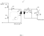
  • FIG. 1 illustrates a converter 1 in accordance with the present disclosure.
  • Technically, the converter 1 comprises a resonant hybrid flyback converter 1 for a light source 2, which may comprise at least one light-emitting diode (LED).
  • A resonant hybrid flyback converter as used herein may refer to a combination of a flyback converter (wherein a square-wave voltage is applied to a primary-side inductance of a transformer) and a resonant converter (wherein the square-wave voltage is applied to a resonant tank circuit), wherein the resonant tank circuit includes the primary-side inductance.
  • In the non-limiting example of FIG. 1, the converter 1 and the light source 2 form part of a luminaire 1, 2.
  • The converter 1 comprises a transformer 101, 102, including a primary-side inductance 101, Lp and a secondary-side inductance 102, Ls. The primary-side inductance 101, Lp may in turn comprise a main inductance 101', Lm and a leakage inductance (not shown).
  • The converter 1 further comprises a high-side switch 103 and a low-side switch 104, connected in series between an input electric potential and a primary-side ground electric potential of the converter 1. The switches 103, 104 may form part of a switching half-bridge (HB) as shown in FIG. 1 or a full bridge (FB), for example.
  • The converter 1 further comprises a resonant tank circuit 101, 105, connected in series between a common electric potential of the switches 103, 104 and the primary-side ground electric potential.
  • The resonant tank circuit 101, 105 comprises an LLC resonant tank including a resonance capacitance 105, Cres in series with the primary-side inductance 101, Lp or more precisely, its main inductance 101', Lm and leakage inductance (not shown).
  • In the non-binding example of FIG. 1, the converter 1 further comprises a half-wave rectifying and smoothing circuit including an output diode D and an output capacitance Cout and connected in parallel to the secondary-side inductance 102, Ls.
  • The converter 1 further comprises a first sensing circuit 110-113 and a second sensing circuit 120-125 (see FIGs. 3, 4).
  • The first sensing circuit 110-113 may comprise a shunt resistance 110, Rshunt (or sense transformer), connected in series to the primary-side inductance 101, Lp. whereas the second sensing circuit 120-125 may comprise an integration resistance 120, Rint in series with an integration capacitance 121, Cint, connected in parallel to the primary-side inductance 101, Lp.
  • The converter 1 further comprises a control circuit 130 (see FIGs. 3, 4), such as an application-specific integrated circuit (ASIC) or the like.
  • As will be explained in more detail below, the control circuit 130 is configured to sense, via the first sensing circuit 110-113, a first voltage 140 being indicative of a resonant current 141, Ires (indicated in FIG. 1 by a circular arrow on a primary side of the transformer 101, 102) through the primary-side inductance 101, Lp.
  • The control circuit 130 is further configured to sense, via the second sensing circuit 120-125, a second voltage 142 being indicative of a magnetizing current 143, Imag (indicated in FIG. 1 by an arrow across the primary-side inductance 101, Lp) through the primary-side inductance 101, Lp.
  • As such, the measurement of the resonant current 141, Ires is done in aid of a shunt, located in the resonant tank, and the measurement of the magnetizing current 143, Imag is done by integration of the voltage across the primary-side inductance 101, Lp of the transformer 101, 102 in aid of an analog integration circuit connected in parallel to the primary-side inductance 101, Lp. Alternatively, the voltage across the primary-side inductance 101, Lp may be measured by an auxiliary winding of the transformer 101, 102 (if any) and an integration by an operational amplifier.
  • To get the same signal amplitudes, the shunt resistance 110, Rshunt, the integration resistance 120, Rint, the integration capacitance 121, Cint and a main inductance 101', Lm of the primary-side inductance 101, Lp may be designed to satisfy Rshunt = Lm / Rint × Cint.
  • The control circuit 130 is further configured to estimate a current 146, ILEDest through the light source 2 in accordance with the first voltage 140 and the second voltage 142.
  • The control circuit 130 is further configured to regulate the current 148, ILED through the light source 2 in accordance with a setpoint value 147, ILEDref and the estimated current 146, ILEDest through the light source 2.
  • Regulation based on the estimated current 146, ILEDest through the light source 2 rather than the actual/measured current 148, ILED through the light source 2 avoids a sensing of the latter and an associated expensive signal transfer across a SELV barrier of the converter 1.
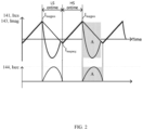
  • FIG. 2 illustrates electrical quantities of the converter 1 of FIG. 1 over the course of time.
  • An upper section shows the resonant current 141, Ires and the magnetizing current 143, Imag through the primary-side inductance 101, Lp, whereas a lower section depicts a current 144, Isec (indicated in FIG. 1 by an arrow on a secondary side of the transformer 101, 102) through the secondary-side inductance 102, Ls.
  • Note the fundamental characteristic of the resonant hybrid flyback converter of the linear increase of the resonant current 141, Ires and the magnetizing current 143, Imag during an on-time of the high-side switch 103. This is different from conventional resonant converters such as LLC converters, for instance. A resonant swing occurs only during an off-time of the high-side switch 103.
  • Further note that resonant hybrid flyback converters differ from conventional resonant converters in a mode of operation of their switches. The latter converters are typically frequency-modulated, wherein both switches are driven alternatingly by a symmetric control signal. The former converters typically involve different control signals. For example, an on-time (conduction time duration) of a control signal of the high-side switch 103 may be regulated in accordance with a load current, whereas a control signal of the low-side switch 104 may depend on a voltage in the resonant tank circuit 101, 105 and/or an instantaneous clocking of the high-side switch 103.
  • An average of the current 144, Isec through the secondary-side inductance 102, Ls corresponds to the current 148, ILED through the light source 2 (i.e., load / LED current).
  • Note that the hatched areas respectively designated as 'A' correspond to one another in terms of size/area. It may thus be concluded that: I sec = I mag I res
    Figure imgb0001
  • In other words, an amount of energy transferred to the light source 2 is determined by a difference of the magnetizing current 143, Imag and the resonant current 141, Ires through the primary-side inductance 101, Lp.
  • Note that the resonant current 141, Ires and the magnetizing current 143, Imag through the primary-side inductance 101, Lp are actually in alignment with one another in terms of their peak currents.
  • FIG. 3 illustrates a converter 1 in accordance with an implementation of the present disclosure.
  • It has been observed that the first voltage 140 and the second voltage 142 differ, due to an impact of the reflected secondary side current during the integration.
  • The observed difference is not constant and depends on the amount of energy transferred to the light source 2. In other words, the estimated current 146, ILEDest through the light source 2 depends on the observed difference.
  • In the implementation of FIG. 3, a common electrical potential of the primary-side inductance 101, Lp and the shunt resistance 110, Rshunt may be connected to a first sensing terminal 131, Sense1 of the control circuit 130.
  • The control circuit 130 may further be configured to sense the first voltage 140 by sampling the first sensing terminal 131, Sense1 for sensing, via the first sensing circuit 110, the first voltage 140 being indicative of the resonant current 141, Ires through the primary-side inductance 101, Lp.
  • Furthermore, a common electric potential of the integration resistance 120, Rint and the integration capacitance 121, Cint may be connected to a second sensing terminal 132, Sense2 of the control circuit 130.
  • The control circuit 130 may further be configured to sense the second voltage 142 by sampling the second sensing terminal 132, Sense2 for sensing, via the second sensing circuit 120-121, the second voltage 142 being indicative of the magnetizing current 143, Imag through the primary-side inductance 101, Lp.
  • In particular, the first voltage 140, VSense1 and the second voltage 142, VSense2 may respectively be sensed using sample and hold (S&H) or track and hold (T&H) circuits.
  • For estimating the current 146, ILEDst through the light source 2 in accordance with the first voltage 140 and the second voltage 142, the control circuit 130 may further be configured to determine a difference 145, dV of the sensed first voltage 140, VSense1 and the sensed second voltage 142, VSense2. dV = V Sense 1 V Sense 2
    Figure imgb0002
  • This differential measurement may take place at any point in time during an on-time of the high-side switch 103.
  • Alternatively, a ground related measurement may be implemented, which has to be done at a zero crossing of the magnetizing current during the on-time of the high-side switch 103. To this end, the control circuit 130 may further be configured to determine the difference 145, dV of the sensed first voltage 140, VSense1 and the sensed second voltage 142, VSense2 by sampling the sensed first voltage 140, VSense1 upon a zero-crossing of the sensed second voltage 142, VSense2 to positive values: dV = V Sense 1 0
    Figure imgb0003
  • The control circuit 130 may further be configured to divide the difference 145, dV by the shunt resistance 110, Rshunt for a conversion from voltage to current; and to multiply a resulting quotient by a turns ratio N of the transformer 101, 102 for a conversion from the primary-side to the secondary-side: I LED = N dV R
    Figure imgb0004
  • FIG. 4 illustrates a converter 1 in accordance with an alternative implementation of the present disclosure, and FIG. 5 illustrates a signal processing in accordance with the implementation of FIG. 4.
  • As previously mentioned, the observed difference the first voltage 140 and the second voltage 142 is not constant and depends on the amount of energy transferred to the light source 2.
  • To calculate the difference between magnetizing current and resonant current, the first voltage 140 and the second voltage 142 may be matched and the required compensation be sensed.
  • In the implementation of FIG. 4, the first sensing circuit 110-113 may further comprise a first offset resistance 111, Roffset1, connected between the common electrical potential of the primary-side inductance 101, Lp and the shunt resistance 110, Rshunt, and a constant current source 133 of the control circuit 130.
  • The first sensing circuit 110-113 may further comprise a first filter resistance 112, Rfilter1 and a first filter capacitance 113, Cfilter1, connected in series between a common electric potential of the first offset resistance 111, Roffset1 and the constant current source 133, and the primary-side ground electric potential.
  • A common electric potential of the first filter resistance 112, Rfilter1 and the first filter capacitance 113, Cfilter1 may be connected to a first sensing terminal 131, Sense1 of the control circuit 130.
  • The second sensing circuit 120-125 may further comprise a second offset resistance 122, Roffset2 and a third offset resistance 123, Roffset3, connected in series between a controllable voltage source 134, DAC of the control circuit 130 and the primary-side ground electric potential.
  • A common electric potential of the second offset resistance 122, Roffset2 and the third offset resistance 123, Roffset3 may be connected to the common electric potential of the integration resistance 120, Rint and the integration capacitance 121, Cint.
  • The second sensing circuit 120-125 may further comprise a second filter resistance 124, Rfilter2 and a second filter capacitance 125, Cfilter2, connected in series between the common electric potential of the second offset resistance 122, Roffset2 and the third offset resistance 123, Roffset3, and the primary-side ground electric potential.
  • The common electric potential of the second filter resistance 124, Rfilter2 and the second filter capacitance 125, Cfilter2 may be connected to a second sensing terminal 132, Sense2 of the control circuit 130.
  • For sensing, via the first sensing circuit 110, the first voltage 140 being indicative of the resonant current 141, Ires through the primary-side inductance 101, Lp, the control circuit 130 may further be configured to sense the first voltage 140 by sampling the first sensing terminal 131, Sense1.
  • For sensing, via the second sensing circuit 120-121, the second voltage 142 being indicative of the magnetizing current 143, Imag through the primary-side inductance 101, Lp, the control circuit 130 may further be configured to sense the second voltage 142 by sampling the second sensing terminal 132, Sense2.
  • This corresponds to a first signal processing phase shown in FIG. 5 wherein the raw the first and second voltages 140, 142 are available.
  • For sensing, via the first sensing circuit 110-113, the first voltage 140 being indicative of the resonant current 141, Ires through the primary-side inductance 101, Lp, the control circuit 130 may further be configured to offset the first voltage 140 to a positive value range by sending a constant current of the current source through the first offset resistance 111, Roffset1; and may further be configured to sense the first voltage 140 by sampling the first sensing terminal 131, Sense1.
  • This corresponds to a second signal processing phase shown in FIG. 5 wherein a default positive shift is applied to first voltages 140.
  • For sensing, via the second sensing circuit 120-125, the second voltage 142 being indicative of the magnetizing current 143, Imag through the primary-side inductance 101, Lp, the control circuit 130 may further be configured to offset the second voltage 142 to correspond to the first voltage 140 in terms of positive peak values by applying a controllable voltage of the controllable voltage source 134, DAC across the second offset resistance 122, Roffset2 and the third offset resistance 123, Roffset3; and sense the second voltage 142 by sampling the second sensing terminal 132, Sense2.
  • This corresponds to a third signal processing phase shown in FIG. 5 wherein the difference between the first and second voltages 140, 142 is actively regulated such that, the difference vanishes and the signals match.
  • For estimating the current 146, ILEDest through the light source 2 in accordance with the first voltage 140 and the second voltage 142, the control circuit 130 may further be configured to average the sensed first voltage 140; average the sensed second voltage 142; and determine a difference 145, dV of the averaged second voltage 142, VSense2 and the averaged first voltage 140, VSense1 by subtracting the latter from the former: dV = V Sense 2 V Sense 1
    Figure imgb0005
  • This corresponds to a fourth signal processing phase shown in FIG. 5.
  • For estimating the current 146, ILEDest through the light source 2 in accordance with the first voltage 140 and the second voltage 142, the control circuit 130 may further be configured to divide the difference 145, dV by the shunt resistance 110, Rshunt, and multiply a resulting quotient by a turns ratio N of the transformer 101, 102: I LED = N dV R
    Figure imgb0006
  • This corresponds to a fifth and last signal processing phase shown in FIG. 5.
  • The present disclosure has been described in conjunction with various implementations as examples. However, other variations can be understood and effected by those persons skilled in the art and practicing the claimed matter, from the studies of the drawings, this disclosure and the independent claims. In the claims as well as in the description the word "comprising" does not exclude other elements or steps and the indefinite article "a" or "an" does not exclude a plurality. A single element or other unit may fulfill the functions of several entities or items recited in the claims. The mere fact that certain measures are recited in the mutual different dependent claims does not indicate that a combination of these measures cannot be used in an advantageous implementation. A computer program may be stored/distributed on a suitable medium, such as an optical storage medium or a solid-state medium supplied together with or as part of other hardware, but may also be distributed in other forms, such as via the Internet or other wired or wireless telecommunication systems.

Claims (13)

  1. A resonant hybrid flyback converter (1) for a light source (2), the converter (1) comprising
    a transformer (101, 102), comprising a primary-side inductance (101, Lp) and a secondary-side inductance (102, Ls);
    a high-side switch (103) and a low-side switch (104), connected in series between an input electric potential and a primary-side ground electric potential of the converter (1);
    a resonant tank circuit (101, 105), connected in series between a common electric potential of the switches (103, 104) and the primary-side ground electric potential, the resonant tank circuit (101, 105) comprising the primary-side inductance (101, Lp);
    a first sensing circuit (110-113);
    a second sensing circuit (120-125); and
    a control circuit (130), configured to
    - sense, via the first sensing circuit (110-113), a first voltage (140) being indicative of a resonant current (141, Ires) through the primary-side inductance (101, Lp);
    - sense, via the second sensing circuit (120-125), a second voltage (142) being indicative of a magnetizing current (143, Imag) through the primary-side inductance (101, Lp);
    - estimate a current (146, ILEDest) through the light source (2) in accordance with the first voltage (140) and the second voltage (142); and
    - regulate the current (148, ILED) through the light source (2) in accordance with a setpoint value (147, ILEDref) and the estimated current (146, ILEDest) through the light source (2).
  2. The converter (1) of claim 1,
    the first sensing circuit (110-113) comprising
    a shunt resistance (110, Rshunt), connected in series to the primary-side inductance (101, Lp).
  3. The converter (1) of claim 2,
    the second sensing circuit (120-125) comprising
    an integration resistance (120, Rint) in series with an integration capacitance (121, Cint), connected in parallel to the primary-side inductance (101, Lp).
  4. The converter (1) of claim 3,
    the shunt resistance (110, Rshunt), the integration resistance (120, Rint), the integration capacitance (121, Cint) and a main inductance (101', Lm) of the primary-side inductance (101, Lp) being designed to satisfy Rshunt = Lm / (Rint × Cint).
  5. The converter (1) of any one of claims 1 - 4,
    a common electrical potential of the primary-side inductance (101, Lp) and the shunt resistance (110, Rshunt) connected to a first sensing terminal (131, Sense1) of the control circuit (130);
    wherein for sensing, via the first sensing circuit (110), the first voltage (140) being indicative of the resonant current (141, Ires) through the primary-side inductance (101, Lp), the control circuit (130) is further configured to
    - sense the first voltage (140) by sampling the first sensing terminal (131, Sense1).
  6. The converter (1) of claim 5,
    a common electric potential of the integration resistance (120, Rint) and the integration capacitance (121, Cint) connected to a second sensing terminal (132, Sense2) of the control circuit (130);
    wherein for sensing, via the second sensing circuit (120-121), the second voltage (142) being indicative of the magnetizing current (143, Imag) through the primary-side inductance (101, Lp), the control circuit (130) is further configured to
    - sense the second voltage (142) by sampling the second sensing terminal (132, Sense2).
  7. The converter (1) of claim 6,
    wherein for estimating the current (146, ILEDest) through the light source (2) in accordance with the first voltage (140) and the second voltage (142), the control circuit (130) is further configured to
    - determine a difference (145, dV) of the sensed first voltage (140) and the sensed second voltage (142) by sampling the sensed first voltage (140) upon a zero-crossing of the sensed second voltage (142) to positive values.
  8. The converter (1) of any one of claims 1 - 4,
    the first sensing circuit (110-113) further comprising
    a first offset resistance (111, Roffset1), connected between the common electrical potential of the primary-side inductance (101, Lp) and the shunt resistance (110, Rshunt), and a constant current source (133) of the control circuit (130); and
    a first filter resistance (112, Rfilter1) and a first filter capacitance (113, Cfilter1), connected in series between a common electric potential of the first offset resistance (111, Roffset1) and the constant current source (133), and the primary-side ground electric potential; a common electric potential of the first filter resistance (112, Rfilter1) and the first filter capacitance (113, Cfilter1) connected to a first sensing terminal (131, Sense1) of the control circuit (130);
    wherein for sensing, via the first sensing circuit (110-113), the first voltage (140) being indicative of the resonant current (141, Ires) through the primary-side inductance (101, Lp), the control circuit (130) is further configured to
    - offset the first voltage (140) to a positive value range by sending a constant current of the current source through the first offset resistance (111, Roffset1); and
    - sense the first voltage (140) by sampling the first sensing terminal (131, Sense1).
  9. The converter (1) of claim 8,
    the second sensing circuit (120-125) further comprising
    a second offset resistance (122, Roffset2) and a third offset resistance (123, Roffset1), connected in series between a controllable voltage source (134, DAC) of the control circuit (130) and the primary-side ground electric potential, a common electric potential of the second offset resistance (122, Roffset2) and the third offset resistance (123, Roffset2) connected to the common electric potential of the integration resistance (120, Rint) and the integration capacitance (121, Cint);
    a second filter resistance (124, Rfilter2) and a second filter capacitance (125, Cfilter2), connected in series between the common electric potential of the second offset resistance (122, Roffset2) and the third offset resistance (123, Roffset1), and the primary-side ground electric potential, the common electric potential of the second filter resistance (124, Rfilter2) and the second filter capacitance (125, Cfilter2) connected to a second sensing terminal (132, Sense2) of the control circuit (130);
    wherein for sensing, via the second sensing circuit (120-125), the second voltage (142) being indicative of the magnetizing current (143, Imag) through the primary-side inductance (101, Lp), the control circuit (130) is further configured to
    - offset the second voltage (142) to correspond to the first voltage (140) in terms of positive peak values by applying a controllable voltage of the controllable voltage source (134, DAC) across the second offset resistance (122, Roffset2) and the third offset resistance (123, Roffset3); and
    - sense the second voltage (142) by sampling the second sensing terminal (132, Sense2).
  10. The converter (1) of claim 9,
    wherein for estimating the current (146, ILEDest) through the light source (2) in accordance with the first voltage (140) and the second voltage (142), the control circuit (130) is further configured to
    - average the sensed first voltage (140);
    - average the sensed second voltage (142); and
    - determine a difference (145, dV) of the averaged first voltage (140) and the averaged second voltage (142) by subtracting the latter from the former.
  11. The converter (1) of claim 7 or claim 10,
    wherein for estimating the current (146, ILEDest) through the light source (2) in accordance with the first voltage (140) and the second voltage (142), the control circuit (130) is further configured to
    - divide the difference (145, dV) by the shunt resistance (110, Rshunt); and
    - multiply a resulting quotient by a turns ratio (N) of the transformer (101, 102).
  12. A luminaire (1, 2), comprising
    a light source (2); and
    a resonant hybrid flyback converter (1) of any one of claims 1 - 11 for the light source (2).
  13. The luminaire (1, 2) of claim 12,
    the light source (2) comprising at least one light-emitting diode, LED.
EP23202323.4A 2023-10-09 2023-10-09 Resonant hybrid flyback converter for a light source, and luminaire Pending EP4539324A1 (en)

Priority Applications (2)

Application Number Priority Date Filing Date Title
EP23202323.4A EP4539324A1 (en) 2023-10-09 2023-10-09 Resonant hybrid flyback converter for a light source, and luminaire
PCT/EP2024/078187 WO2025078321A1 (en) 2023-10-09 2024-10-08 Resonant hybrid flyback converter for a light source, and luminaire

Applications Claiming Priority (1)

Application Number Priority Date Filing Date Title
EP23202323.4A EP4539324A1 (en) 2023-10-09 2023-10-09 Resonant hybrid flyback converter for a light source, and luminaire

Publications (1)

Publication Number Publication Date
EP4539324A1 true EP4539324A1 (en) 2025-04-16

Family

ID=88297022

Family Applications (1)

Application Number Title Priority Date Filing Date
EP23202323.4A Pending EP4539324A1 (en) 2023-10-09 2023-10-09 Resonant hybrid flyback converter for a light source, and luminaire

Country Status (2)

Country Link
EP (1) EP4539324A1 (en)
WO (1) WO2025078321A1 (en)

Citations (5)

* Cited by examiner, † Cited by third party
Publication number Priority date Publication date Assignee Title
US8199534B2 (en) * 2007-02-27 2012-06-12 Nxp B.V. Load current detection in electrical power converters
WO2015103659A2 (en) * 2014-01-13 2015-07-16 Tridonic Gmbh & Co Kg Driver circuit for lighting means, particularly leds
WO2018104087A1 (en) * 2016-12-07 2018-06-14 Tridonic Gmbh & Co Kg Circuit assembly and method for operating a lighting means
US20200021200A1 (en) * 2018-07-12 2020-01-16 Infineon Technologies Austria Ag Flyback converter controller, flyback converter and method of operating the flyback converter
WO2023144037A1 (en) * 2022-01-26 2023-08-03 Tridonic Gmbh & Co Kg A switched converter

Patent Citations (5)

* Cited by examiner, † Cited by third party
Publication number Priority date Publication date Assignee Title
US8199534B2 (en) * 2007-02-27 2012-06-12 Nxp B.V. Load current detection in electrical power converters
WO2015103659A2 (en) * 2014-01-13 2015-07-16 Tridonic Gmbh & Co Kg Driver circuit for lighting means, particularly leds
WO2018104087A1 (en) * 2016-12-07 2018-06-14 Tridonic Gmbh & Co Kg Circuit assembly and method for operating a lighting means
US20200021200A1 (en) * 2018-07-12 2020-01-16 Infineon Technologies Austria Ag Flyback converter controller, flyback converter and method of operating the flyback converter
WO2023144037A1 (en) * 2022-01-26 2023-08-03 Tridonic Gmbh & Co Kg A switched converter

Also Published As

Publication number Publication date
WO2025078321A1 (en) 2025-04-17

Similar Documents

Publication Publication Date Title
US10326377B1 (en) Circuit and method for indirect primary-side load current sensing in an isolated power supply
US8044643B1 (en) Power supply switching circuit for a halogen lamp
US9923409B2 (en) Rectification and regulation circuit for a wireless power receiver
US6751107B2 (en) DC power supply device with constant power output level
US7994736B2 (en) Cold cathode fluorescent lamp inverter apparatus
US6549436B1 (en) Integrated magnetic converter circuit and method with improved filtering
US9787195B1 (en) Primary current sensing method for isolated LED driver
KR20060083162A (en) Multi-Output DC-DC Converters
EP0658968A1 (en) Switching regulator
JPH07298636A (en) Self-excited inverter
US10658932B2 (en) Power control circuit
US20070274105A1 (en) Switching Power Supply Apparatus
TWI516007B (en) DC power supply unit
JP2012170218A (en) Switching power supply device
EP4539324A1 (en) Resonant hybrid flyback converter for a light source, and luminaire
US20250158515A1 (en) Llc voltage converter
EP4535632A1 (en) Resonant hybrid flyback converter for a light source, and luminaire
WO2025078338A1 (en) Resonant hybrid flyback converter for a light source, and luminaire
JP4720514B2 (en) Current detection method in resonant converter
JP3463278B2 (en) Power supply
US5434769A (en) Multi-phase adaptable AC-DC converter
EP1313203A2 (en) Half-bridge converters
EP3967110B1 (en) Led converter
WO2020255720A1 (en) Isolated dc-dc converter
JP2677738B2 (en) Switching regulator

Legal Events

Date Code Title Description
PUAI Public reference made under article 153(3) epc to a published international application that has entered the european phase

Free format text: ORIGINAL CODE: 0009012

STAA Information on the status of an ep patent application or granted ep patent

Free format text: STATUS: THE APPLICATION HAS BEEN PUBLISHED

AK Designated contracting states

Kind code of ref document: A1

Designated state(s): AL AT BE BG CH CY CZ DE DK EE ES FI FR GB GR HR HU IE IS IT LI LT LU LV MC ME MK MT NL NO PL PT RO RS SE SI SK SM TR

STAA Information on the status of an ep patent application or granted ep patent

Free format text: STATUS: REQUEST FOR EXAMINATION WAS MADE

17P Request for examination filed

Effective date: 20250811

STAA Information on the status of an ep patent application or granted ep patent

Free format text: STATUS: EXAMINATION IS IN PROGRESS

17Q First examination report despatched

Effective date: 20251209
