CROSS-REFERENCE TO RELATED APPLICATION
-
This application claims the benefit of Chinese Patent Application No.
CN202311330105.9 filed on October 13, 2023 in the State Intellectual Property Office of China, the whole disclosure of which is incorporated herein by reference.
BACKGROUND OF THE INVENTION
Field of the Invention
-
The present invention relates to a connector terminal, a method for manufacturing the connector terminal, and a connector comprising the connector terminal.
Description of the Related Art
-
In the prior art, in order to improve the electrical contact performance of the connector terminal, it is usually necessary to form an electroplating layer on the entire or local surface of the connector terminal, which can be a copper electroplating layer, a silver-electroplating layer, or a gold electroplating layer. When the connector terminal is in electrical contact with the mating connector terminal, the electroplating layer on the connector terminal is in electrical contact with the electroplating layer on the mating connector terminal, thereby improving the electrical contact performance between the connector terminal and the mating connector terminal. In the prior art, as the electroplating layer is directly formed on the connector terminal, each connector terminal needs to be separately electroplated, which greatly reduces manufacturing efficiency and increases manufacturing costs.
SUMMARY OF THE INVENTION
-
The present invention has been made to overcome or alleviate at least one aspect of the above mentioned disadvantages.
-
According to an aspect of the present invention, there is provided a connector terminal. The connector terminal comprises a terminal body and an electroplated component. The electroplated component includes: a substrate layer which has a first and second surface opposite to each other in its thickness direction, wherein the first surface of the substrate layer is attached to a local area of the terminal body; and an electroplating layer which is formed on the second surface of the substrate layer for electrical contact with a mating terminal.
-
According to an exemplary embodiment of the present invention, the substrate layer of the electroplated component is welded, riveted, or crimped onto the local area of the terminal body.
-
According to another exemplary embodiment of the present invention, the terminal body is flat and has a pair of surfaces opposite to each other in its thickness direction, and the electroplated component is sheet-like and attached to the surface of the terminal body.
-
According to another exemplary embodiment of the present invention, the terminal body is cylindrical, and the electroplated component is hollow cylindrical and is sheathed on the terminal body; the inner peripheral surface of the substrate layer of the electroplated component is attached to the outer peripheral surface of the terminal body, and the electroplating layer is formed on the outer peripheral surface of the substrate layer of the electroplated component.
-
According to another exemplary embodiment of the present invention, the terminal body is in a hollow cylindrical shape, and the electroplated component is in a ring shape and inserted into an inner cavity of the terminal body; the outer peripheral surface of the substrate layer of the electroplated component is attached to the inner peripheral surface of the terminal body, and the electroplating layer is formed on the inner peripheral surface of the substrate layer of the electroplated component.
-
According to another exemplary embodiment of the present invention, the terminal body is in a flat shape, comprising a pair of surfaces opposite to each other in its thickness direction and two ends opposite to each other in its longitudinal direction; the substrate layer of the electroplated component is U-shaped, comprising a pair of flat plate parts and a bent part connected between the pair of flat plate parts, and the electroplating layer is formed on the outer surface of the substrate layer of the electroplated component; one end of the terminal body is inserted into the electroplated component, and the inner surfaces of the pair of flat plate parts of the electroplated component are respectively attached to the pair of surfaces of the terminal body, the inner surface of the bent part of the electroplated component is attached to an end face of the terminal body.
-
According to another exemplary embodiment of the present invention, the terminal body is in a flat shape, comprising a pair of surfaces opposite to each other in its thickness direction and two opposite sides in its transverse direction; the substrate layer of the electroplated component is U-shaped, comprising a pair of flat plate parts and a bent part connected between the pair of flat plate parts, and the electroplating layer is formed on the outer surface of the substrate layer of the electroplated component; the terminal body is inserted into the electroplated component along its transverse direction, and the inner surfaces of the pair of flat plate parts of the electroplated component are respectively attached to the pair of surfaces of the terminal body, and the inner surface of the bent part of the electroplated component is attached to one side of the terminal body.
-
According to another exemplary embodiment of the present invention, the terminal body is block shaped and formed with a slot that allows for the insertion of a mating terminal, and the electroplated component is sheet shaped and attached to the inner surface of the slot of the terminal body.
-
According to another exemplary embodiment of the present invention, the connector terminal comprises two electroplated components, which are respectively attached to the two inner sides of the slot of the terminal body to make electrical contact with both sides of the mating terminal inserted into the slot.
-
According to another exemplary embodiment of the present invention, a recess is formed on the terminal body suitable for mating with the electroplated component, and the electroplated component is embedded in the recess of the terminal body.
-
According to another aspect of the present invention, there is provided a connector. The connector comprises: a housing; and the above connector terminal which is provided in the housing.
-
According to another aspect of the present invention, there is provided a method for manufacturing a connector terminal. The method comprises following steps of:
- S 100: manufacturing a terminal body and an electroplated component separately; and
- S200: attaching the electroplated component to a local area of the terminal body.
-
According to an exemplary embodiment of the present invention, manufacturing the electroplated component comprises the following steps of:
- S110: providing a substrate plate;
- S120: forming an electroplating layer on one surface of the substrate plate; and
- S130: stamping the substrate plate on which the electroplating layer has been formed to obtain one or more electroplated component.
-
In the aforementioned exemplary embodiments of the present invention, the electroplating layer for electrical contact is formed on the electroplated component separated from the terminal body, thus eliminating the need for electroplating on the terminal body, improving manufacturing efficiency and reducing manufacturing costs.
BRIEF DESCRIPTION OF THE DRAWINGS
-
The above and other features of the present invention will become more apparent by describing in detail exemplary embodiments thereof with reference to the accompanying drawings, in which:
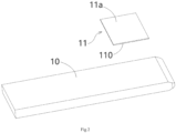
- Figure 1 shows an illustrative perspective view of a connector terminal according to the first embodiment of the present invention;
- Figure 2 shows an illustrative exploded view of the connector terminals according to the first embodiment of the present invention;
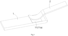
- Figure 3 shows an illustrative view of the electrical contact between the connector terminal and the mating terminal according to the first embodiment of the present invention;
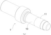
- Figure 4 shows an illustrative perspective view of a connector terminal according to a second embodiment of the present invention;
- Figure 5 shows an illustrative exploded view of the connector terminals according to the second embodiment of the present invention;
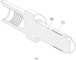
- Figure 6 shows a longitudinal sectional view of a connector terminal according to a second embodiment of the present invention;
- Figure 7 shows an illustrative perspective view of a connector terminal according to a third embodiment of the present invention;
- Figure 8 shows an illustrative exploded view of the connector terminals according to the third embodiment of the present invention;
- Figure 9 shows an illustrative perspective view of a connector terminal according to a fourth embodiment of the present invention;
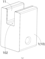
- Figure 10 shows an illustrative exploded view of the connector terminals according to the fourth embodiment of the present invention;
- Figure 11 shows an illustrative perspective view of a connector terminal according to a fifth embodiment of the present invention;
- Figure 12 shows an illustrative exploded view of the connector terminals according to the fifth embodiment of the present invention;
- Figure 13 shows an illustrative perspective view of a connector terminal according to a sixth embodiment of the present invention; and
- Figure 14 shows an illustrative exploded view of the connector terminals according to the sixth embodiment of the present invention.
DETAILED DESCRIPTION OF PREFERRED EMBODIMENTS OF THE IVENTION
-
Exemplary embodiments of the present disclosure will be described hereinafter in detail with reference to the attached drawings, wherein the like reference numerals refer to the like elements. The present disclosure may, however, be embodied in many different forms and should not be construed as being limited to the embodiment set forth herein; rather, these embodiments are provided so that the present disclosure will be thorough and complete, and will fully convey the concept of the disclosure to those skilled in the art.
-
In the following detailed description, for purposes of explanation, numerous specific details are set forth in order to provide a thorough understanding of the disclosed embodiments. It will be apparent, however, that one or more embodiments may be practiced without these specific details. In other instances, well-known structures and devices are schematically shown in order to simplify the drawing.
-
According to a general concept of the present invention, there is provided a connector terminal. The connector terminal comprises a terminal body and an electroplated component. The electroplated component includes: a substrate layer which has a first and second surface opposite to each other in its thickness direction, wherein the first surface of the substrate layer is attached to a local area of the terminal body; and an electroplating layer which is formed on the second surface of the substrate layer for electrical contact with a mating terminal.
-
According to another general concept of the present invention, there is provided a connector. The connector comprises: a housing; and the above connector terminal which is provided in the housing.
-
According to another general concept of the present invention, there is provided a method for manufacturing a connector terminal. The method comprises of manufacturing a terminal body and an electroplated component separately; and attaching the electroplated component to a local area of the terminal body.
First Embodiment
-
Figures 1 to 3 show a connector terminal 1 according to the first embodiment of the present invention. Among them, Figure 1 shows an illustrative perspective view of connector terminal 1 according to the first embodiment of the present invention; Figure 2 shows an illustrative exploded view of connector terminal 1 according to the first embodiment of the present invention; Figure 3 shows an illustrative view of electrical contact between connector terminal 1 and mating terminal 2 according to the first embodiment of the present invention.
-
As shown in Figures 1 to 3, in an exemplary embodiment of the present invention, a connector terminal 1 is disclosed. The connector terminal 1 includes: a terminal body 10 and an electroplated component 11. The electroplated component 11 includes a substrate layer 110 and an electroplating layer 11a. The substrate layer 110 has a first surface and a second surface opposite to each other in its thickness direction, and the first surface of the substrate layer 110 is attached to a local area of the terminal body 10. The electroplating layer 11a is formed on the second surface of the substrate layer 110 for electrical contact with a mating terminal 2.
-
As shown in Figures 1 to 3, in the illustrated embodiments, the conductivity of the electroplating layer 11a of the electroplated component 11 is superior to that of the substrate layer 110 of the electroplated component 11 and the terminal body 10.
-
As shown in Figures 1 to 3, in an exemplary embodiment of the present invention, the substrate layer 110 of the electroplated component 11 and the terminal body 10 may be made of the same or different materials. For example, in order to reduce manufacturing costs, the substrate layer 110 of the electroplated component 11 and the terminal body 10 can both be made of aluminum, and the electroplating layer 11a of electroplated component 11 can be a copper electroplating layer, a silver electroplating layer, or a gold electroplating layer.
-
As shown in Figures 1 to 3, in the illustrated embodiments, the substrate layer 110 of the electroplated component 11 can be welded, riveted, or crimped onto a local area of the terminal body 10. For example, the substrate layer 110 of electroplated component 11 can be welded to a local area of the terminal body 10 using ultrasonic welding technology.
-
As shown in Figures 1 to 3, in the illustrated embodiments, the terminal body 10 is flat and has a pair of surfaces opposite to each other in its thickness direction, and the electroplated component 11 is sheet-like and attached to the surface of the terminal body 10.
-
Although not illustrated, in the illustrated embodiment, a recess suitable for fitting with the electroplated component 11 can be formed on the terminal body 10, and the electroplated component 11 is embedded in the recess of the terminal body 10.
-
As shown in Figures 1 to 3, in another exemplary embodiment of the present invention, a connector is also disclosed. The connector includes a housing (not shown) and the connector terminal 1. The connector terminal 1 is provided in the housing.
-
As shown in Figures 1 to 3, in another exemplary embodiment of the present invention, a method for manufacturing a connector terminal is also disclosed. This method mainly includes the following steps of:
- S 100: manufacturing a terminal body 10 and an electroplated component 11 separately; and
- S200: attaching the electroplated component 11 to a local area of the terminal body 10.
-
As shown in Figures 1 to 3, in the illustrated embodiments, manufacturing the electroplated component 11 comprises the following steps of:
- S110: providing a substrate plate;
- S120: forming an electroplating layer 11a on one surface of the substrate plate; and
- S130: stamping the substrate plate on which the electroplating layer 11a has been formed to obtain one or more electroplated component 11.
Second Embodiment
-
Figures 4 to 6 show a connector terminal according to a second embodiment of the present invention. Among them, Figure 4 shows an illustrative perspective view of a connector terminal according to the second embodiment of the present invention; Figure 5 shows an illustrative exploded view of the connector terminals according to the second embodiment of the present invention; Figure 6 shows a longitudinal sectional view of a connector terminal according to a second embodiment of the present invention.
-
As shown in Figures 4 to 6, in an exemplary embodiment of the present invention, a connector terminal 1 is disclosed. The connector terminal 1 includes: a terminal body 10 and an electroplated component 11. The electroplated component 11 includes a substrate layer 110 and an electroplating layer 11a. The substrate layer 110 has a first surface and a second surface opposite to each other in its thickness direction, and the first surface of the substrate layer 110 is attached to a local area of the terminal body 10. The electroplating layer 11a is formed on the second surface of the substrate layer 110 for electrical contact with a mating terminal (not shown).
-
As shown in Figures 4 to 6, in the illustrated embodiments, the conductivity of the electroplating layer 11a of the electroplated component 11 is superior to that of the substrate layer 110 of the electroplated component 11 and the terminal body 10.
-
As shown in Figures 4 to 6, in an exemplary embodiment of the present invention, the substrate layer 110 of the electroplated component 11 and the terminal body 10 may be made of the same or different materials. For example, in order to reduce manufacturing costs, the substrate layer 110 of the electroplated component 11 and the terminal body 10 can both be made of aluminum, and the electroplating layer 11a of the electroplated component 11 can be a copper electroplating layer, a silver electroplating layer, or a gold electroplating layer.
-
As shown in Figures 4 to 6, in the illustrated embodiments, the substrate layer 110 of the electroplated component 11 can be welded, riveted, or crimped onto a local area of the terminal body 10. For example, the substrate layer 110 of electroplated component 11 can be welded to a local area of the terminal body 10 using ultrasonic welding technology.
-
As shown in Figures 4 to 6, in the illustrated embodiments, the terminal body 10 is cylindrical, and the electroplated component 11 is hollow cylindrical and is mounted on the terminal body 10. The inner surface of the substrate layer 110 of the electroplated component 11 is attached to the outer surface of the terminal body 10, and the electroplating layer 11a is formed on the outer surface of the substrate layer 110 of the electroplated component 11.
-
As shown in Figures 4 to 6, in the illustrated embodiments, a recess 101 suitable for mating with the electroplated component 11 is formed on the outer surface of the terminal body 10, and the electroplated component 11 is embedded in the recess 101 of the terminal body 10.
-
As shown in Figures 4 to 6, in another exemplary embodiment of the present invention, a connector is also disclosed. The connector includes a housing (not shown) and the connector terminal 1. The connector terminal 1 is provided in the housing.
-
As shown in Figures 4 to 6, in another exemplary embodiment of the present invention, a method for manufacturing the connector terminal is also disclosed. This method mainly includes the following steps of:
- S100: manufacturing a terminal body 10 and an electroplated component 11 separately; and
- S200: attaching the electroplated component 11 to a local area of the terminal body 10.
-
As shown in Figures 4 to 6, in the illustrated embodiments, manufacturing the electroplated component 11 comprises the following steps of:
- S110: providing a substrate plate;
- S120: forming an electroplating layer 11a on one surface of the substrate plate; and
- S130: stamping the substrate plate on which the electroplating layer 11a has been formed to obtain one or more electroplated component 11.
Third Embodiment
-
Figures 7 and 8 show connector terminals according to a third embodiment of the present invention. Among them, Figure 7 shows an illustrative perspective view of a connector terminal according to the third embodiment of the present invention; Figure 8 shows an illustrative exploded view of the connector terminals according to the third embodiment of the present invention.
-
As shown in Figures 7 and 8, in an exemplary embodiment of the present invention, a connector terminal 1 is disclosed. The connector terminal 1 includes: a terminal body 10 and an electroplated component 11. The electroplated component 11 includes a substrate layer 110 and an electroplating layer 11a. The substrate layer 110 has a first surface and a second surface opposite to each other in its thickness direction, and the first surface of the substrate layer 110 is attached to a local area of the terminal body 10. The electroplating layer 11a is formed on the second surface of the substrate layer 110 for electrical contact with a mating terminal (not shown).
-
As shown in Figures 7 and 8, in the illustrated embodiments, the conductivity of the electroplating layer 11a of the electroplated component 11 is superior to that of the substrate layer 110 of the electroplated component 11 and the terminal body 10.
-
As shown in Figures 7 and 8, in an exemplary embodiment of the present invention, the substrate layer 110 of the electroplated component 11 and the terminal body 10 may be made of the same or different materials. For example, in order to reduce manufacturing costs, the substrate layer 110 of the electroplated component 11 and the terminal body 10 can both be made of aluminum, and the electroplating layer 11a of electroplated component 11 can be a copper electroplating layer, a silver electroplating layer, or a gold electroplating layer.
-
As shown in Figures 7 and 8, in the illustrated embodiments, the substrate layer 110 of the electroplated component 11 can be welded, riveted, or crimped onto a local area of the terminal body 10. For example, the substrate layer 110 of electroplated component 11 can be welded to a local area of the terminal body 10 using ultrasonic welding technology.
-
As shown in Figures 7 and 8, in the illustrated embodiments, the terminal body 10 is in a flat shape, comprising a pair of opposite surfaces in its thickness direction and two opposite ends in its longitudinal direction. The substrate layer 110 of electroplated component 11 is U-shaped, including a pair of flat plate parts 111 and a bent part 112 connected between the pair of flat plate parts 111. The electroplating layer 11a is formed on the outer surface of the substrate layer 110 of the electroplated component 11. One end of the terminal body 10 is inserted into the electroplated component 11, and the inner surfaces of the pair of flat plate parts 111 of the electroplated component 11 are respectively attached to the pair of surfaces of the terminal body 10. The inner surfaces of the bending part 112 of the electroplated component 11 are attached to an end face of the terminal body 10.
-
Although not illustrated, in the illustrated embodiment, a recess suitable for fitting with the electroplated component 11 can be formed on the terminal body 10, and the electroplated component 11 is embedded in the recess of the terminal body 10.
-
As shown in Figures 7 and 8, in another exemplary embodiment of the present invention, a connector is also disclosed. The connector includes a housing (not shown) and the connector terminal 1. The connector terminal 1 is provided in the housing.
-
As shown in Figures 7 and 8, in another exemplary embodiment of the present invention, a method for manufacturing the connector terminal is also disclosed. This method mainly includes the following steps of:
- S100: manufacturing a terminal body 10 and an electroplated component 11 separately; and
- S200: attaching the electroplated component 11 to a local area of the terminal body 10.
-
As shown in Figures 7 and 8, in the illustrated embodiments, manufacturing the electroplated component 11 comprises the following steps of:
- S110: providing a substrate plate;
- S120: forming an electroplating layer 11a on one surface of the substrate plate; and
- S130: stamping the substrate plate on which the electroplating layer 11a has been formed to obtain one or more electroplated component 11.
Fourth Embodiment
-
Figures 9 and 10 show the connector terminals according to the fourth embodiment of the present invention. Among them, Figure 9 shows an illustrative perspective view of a connector terminal according to the fourth embodiment of the present invention; Figure 10 shows an illustrative exploded view of the connector terminals according to the fourth embodiment of the present invention.
-
As shown in Figures 9 and 10, in an exemplary embodiment of the present invention, a connector terminal 1 is disclosed. The connector terminal 1 includes: a terminal body 10 and an electroplated component 11. The electroplated component 11 includes a substrate layer 110 and an electroplating layer 11a. The substrate layer 110 has a first surface and a second surface opposite to each other in its thickness direction, and the first surface of the substrate layer 110 is attached to a local area of the terminal body 10. The electroplating layer 11a is formed on the second surface of the substrate layer 110 for electrical contact with a mating terminal (not shown).
-
As shown in Figures 9 and 10, in the illustrated embodiments, the conductivity of the electroplating layer 11a of the electroplated component 11 is superior to that of the substrate layer 110 of the electroplated component 11 and the terminal body 10.
-
As shown in Figures 9 and 10, in an exemplary embodiment of the present invention, the substrate layer 110 of the electroplated component 11 and the terminal body 10 may be made of the same or different materials. For example, in order to reduce manufacturing costs, the substrate layer 110 of the electroplated component 11 and the terminal body 10 can both be made of aluminum, and the electroplating layer 11a of electroplated component 11 can be a copper electroplating layer, a silver electroplating layer, or a gold electroplating layer.
-
As shown in Figures 9 and 10, in the illustrated embodiments, the substrate layer 110 of the electroplated component 11 can be welded, riveted, or crimped onto a local area of the terminal body 10. For example, the substrate layer 110 of electroplated component 11 can be welded to a local area of the terminal body 10 using ultrasonic welding technology.
-
As shown in Figures 9 and 10, in the illustrated embodiments, the terminal body 10 is in a block shape and formed with a slot 102 that allows for the insertion of a mating terminal (not shown), and the electroplated component 11 is in a sheet shape and attached to the inner surface of the slot 102 of the terminal body 10.
-
As shown in Figures 9 and 10, in the illustrated embodiment, the connector terminal 1 comprises two electroplated component 11, which are respectively attached to the two inner sides of the slot 102 of the terminal body 10 to make electrical contact with both sides of the mating terminal (not shown) inserted into the slot 102.
-
Although not illustrated, in the illustrated embodiment, a recess suitable for fitting with the electroplated component 11 can be formed on the terminal body 10, and the electroplated component 11 is embedded in the recess of the terminal body 10.
-
As shown in Figures 9 and 10, in another exemplary embodiment of the present invention, a connector is also disclosed. The connector includes a housing (not shown) and the connector terminal 1. The connector terminal 1 is provided in the housing.
-
As shown in Figures 9 and 10, in another exemplary embodiment of the present invention, a method for manufacturing the connector terminal is also disclosed. This method mainly includes the following steps of:
- S100: manufacturing a terminal body 10 and an electroplated component 11 separately; and
- S200: attaching the electroplated component 11 to a local area of the terminal body 10.
-
As shown in Figures 9 and 10, in the illustrated embodiments, manufacturing the electroplated component 11 comprises the following steps:
- S110: providing a substrate plate;
- S120: forming an electroplating layer 11a on one surface of the substrate plate; and
- S130: stamping the substrate plate on which the electroplating layer 11a has been formed to obtain one or more electroplated component 11.
Fifth Embodiment
-
Figures 11 and 12 show connector terminals according to a fifth embodiment of the present invention. Among them, Figure 11 shows an illustrative perspective view of a connector terminal according to the fifth embodiment of the present invention; Figure 12 shows an illustrative exploded view of the connector terminals according to the fifth embodiment of the present invention.
-
As shown in Figures 11 and 12, in an exemplary embodiment of the present invention, a connector terminal 1 is disclosed. The connector terminal 1 includes: a terminal body 10 and an electroplated component 11. The electroplated component 11 includes a substrate layer 110 and an electroplating layer 11a. The substrate layer 110 has a first surface and a second surface opposite to each other in its thickness direction, and the first surface of the substrate layer 110 is attached to a local area of the terminal body 10. The electroplating layer 11a is formed on the second surface of the substrate layer 110 for electrical contact with a mating terminal (not shown).
-
As shown in Figures 11 and 12, in the illustrated embodiments, the conductivity of the electroplating layer 11a of the electroplated component 11 is superior to that of the substrate layer 110 of the electroplated component 11 and the terminal body 10.
-
As shown in Figures 11 and 12, in an exemplary embodiment of the present invention, the substrate layer 110 of the electroplated component 11 and the terminal body 10 may be made of the same or different materials. For example, in order to reduce manufacturing costs, the substrate layer 110 of the electroplated component 11 and the terminal body 10 can both be made of aluminum, and the electroplating layer 11a of electroplated component 11 can be a copper electroplating layer, a silver electroplating layer, or a gold electroplating layer.
-
As shown in Figures 11 and 12, in the illustrated embodiments, the substrate layer 110 of the electroplated component 11 can be welded, riveted, or crimped onto a local area of the terminal body 10. For example, the substrate layer 110 of electroplated component 11 can be welded to a local area of the terminal body 10 using ultrasonic welding technology.
-
As shown in Figures 11 and 12, in the illustrated embodiments, the terminal body 10 is in a flat shape, comprising a pair of opposite surfaces in its thickness direction and two opposite sides in its transverse direction. The substrate layer 110 of electroplated component 11 is U-shaped, including a pair of flat plate parts 111 and a bent part 112 connected between the pair of flat plate parts 111. The electroplating layer 11a is formed on the outer surface of the substrate layer 110 of the electroplated component 11. The terminal body 10 is inserted into the electroplated component 11 along the transverse direction, and the inner surfaces of the pair of flat plate parts 111 of the electroplated component 11 are respectively attached to the pair of surfaces of the terminal body 10. The inner surfaces of the bending part 112 of the electroplated component 11 are attached to one side of the terminal body 10.
-
Although not illustrated, in the illustrated embodiment, a recess suitable for fitting with the electroplated component 11 can be formed on the terminal body 10, and the electroplated component 11 is embedded in the recess of the terminal body 10.
-
As shown in Figures 11 and 12, in another exemplary embodiment of the present invention, a connector is also disclosed. The connector includes a housing (not shown) and the connector terminal 1. The connector terminal 1 is provided in the housing.
-
As shown in Figures 11 and 12, in another exemplary embodiment of the present invention, a method for manufacturing the connector terminal is also disclosed. This method mainly includes the following steps of:
- S100: manufacturing a terminal body 10 and an electroplated component 11 separately; and
- S200: attaching the electroplated component 11 to a local area of terminal body 10.
-
As shown in Figures 11 and 12, in the illustrated embodiments, manufacturing the electroplated component 11 comprises the following steps of:
- S110: providing a substrate plate;
- S120: forming an electroplating layer 11a on one surface of the substrate plate; and
- S130: stamping a substrate plate on which the electroplating layer 11a has been formed to obtain one or more electroplated component 11.
Sixth Embodiment
-
Figures 13 and 14 show connector terminals according to a sixth embodiment of the present invention. Among them, Figure 13 shows an illustrative perspective view of a connector terminal according to the sixth embodiment of the present invention; Figure 5 shows an illustrative exploded view of the connector terminals according to the sixth embodiment of the present invention.
-
As shown in Figures 13 and 14, in an exemplary embodiment of the present invention, a connector terminal 1 is disclosed. The connector terminal 1 includes: a terminal body 10 and an electroplated component 11. The electroplated component 11 includes a substrate layer 110 and an electroplating layer 11a. The substrate layer 110 has a first surface and a second surface opposite to each other in its thickness direction, and the first surface of the substrate layer 110 is attached to a local area of the terminal body 10. The electroplating layer 11a is formed on the second surface of the substrate layer 110 for electrical contact with a mating terminal (not shown).
-
As shown in Figures 13 and 14, in the illustrated embodiments, the conductivity of the electroplating layer 11a of the electroplated component 11 is superior to that of the substrate layer 110 of the electroplated component 11 and the terminal body 10.
-
As shown in Figures 13 and 14, in an exemplary embodiment of the present invention, the substrate layer 110 of the electroplated component 11 and the terminal body 10 may be made of the same or different materials. For example, in order to reduce manufacturing costs, the substrate layer 110 of the electroplated component 11 and the terminal body 10 can both be made of aluminum, and the electroplating layer 11a of electroplated component 11 can be a copper electroplating layer, a silver electroplating layer, or a gold electroplating layer.
-
As shown in Figures 13 and 14, in the illustrated embodiments, the substrate layer 110 of the electroplated component 11 can be welded, riveted, or crimped onto a local area of the terminal body 10. For example, the substrate layer 110 of electroplated component 11 can be welded to a local area of the terminal body 10 using ultrasonic welding technology.
-
As shown in Figures 13 and 14, in the illustrated embodiments, the terminal body 10 is in a hollow cylindrical shape, and the electroplated component 11 is in a ring shape and inserted into the inner cavity 103 of the terminal body 10. The outer peripheral surface of the substrate layer 110 of the electroplated component 11 is attached to the inner peripheral surface of the terminal body 10, and the electroplating layer 11a is formed on the inner peripheral surface of the substrate layer 110 of the electroplated component 11.
-
Although not shown, a recess suitable for fitting with the electroplated component 11 can be formed on the inner surface of the terminal body 10, and the electroplated component 11 is embedded in the recess of the terminal body 10.
-
As shown in Figures 13 and 14, in another exemplary embodiment of the present invention, a connector is also disclosed. The connector includes a housing (not shown) and the connector terminal 1. The connector terminal 1 is provided in the housing.
-
As shown in Figures 13 and 14, in another exemplary embodiment of the present invention, a method for manufacturing the connector terminal is also disclosed. This method mainly includes the following steps of:
- S100: manufacturing a terminal body 10 and an electroplated component 11 separately; and
- S200: attaching the electroplated component 11 to a local area of the terminal body 10.
-
As shown in Figures 13 and 14, in the illustrated embodiments, manufacturing the electroplated component 11 comprises the following steps of:
- S110: providing a substrate plate;
- S120: forming an electroplating layer 11a on one surface of the substrate plate; and
- S130: stamping the substrate plate on which the electroplating layer 11a has been formed to obtain one or more electroplated component 11.
-
It should be appreciated for those skilled in this art that the above embodiments are intended to be illustrated, and not restrictive. For example, many modifications may be made to the above embodiments by those skilled in this art, and various features described in different embodiments may be freely combined with each other without conflicting in configuration or principle.
-
Although several exemplary embodiments have been shown and described, it would be appreciated by those skilled in the art that various changes or modifications may be made in these embodiments without departing from the principles and spirit of the disclosure, the scope of which is defined in the claims and their equivalents.
-
As used herein, an element recited in the singular and proceeded with the word "a" or "an" should be understood as not excluding plural of said elements or steps, unless such exclusion is explicitly stated. Furthermore, references to "one embodiment" of the present invention are not intended to be interpreted as excluding the existence of additional embodiments that also incorporate the recited features. Moreover, unless explicitly stated to the contrary, embodiments "comprising" or "having" an element or a plurality of elements having a particular property may include additional such elements not having that property.