EP4539105A1 - Silicon carbide single crystal substrate processing method, and silicon carbide single crystal substrate processing system - Google Patents
Silicon carbide single crystal substrate processing method, and silicon carbide single crystal substrate processing system Download PDFInfo
- Publication number
- EP4539105A1 EP4539105A1 EP23831306.8A EP23831306A EP4539105A1 EP 4539105 A1 EP4539105 A1 EP 4539105A1 EP 23831306 A EP23831306 A EP 23831306A EP 4539105 A1 EP4539105 A1 EP 4539105A1
- Authority
- EP
- European Patent Office
- Prior art keywords
- single crystal
- crystal substrate
- silicon carbide
- carbide single
- treating
- Prior art date
- Legal status (The legal status is an assumption and is not a legal conclusion. Google has not performed a legal analysis and makes no representation as to the accuracy of the status listed.)
- Pending
Links
Images


Classifications
-
- C—CHEMISTRY; METALLURGY
- C30—CRYSTAL GROWTH
- C30B—SINGLE-CRYSTAL GROWTH; UNIDIRECTIONAL SOLIDIFICATION OF EUTECTIC MATERIAL OR UNIDIRECTIONAL DEMIXING OF EUTECTOID MATERIAL; REFINING BY ZONE-MELTING OF MATERIAL; PRODUCTION OF A HOMOGENEOUS POLYCRYSTALLINE MATERIAL WITH DEFINED STRUCTURE; SINGLE CRYSTALS OR HOMOGENEOUS POLYCRYSTALLINE MATERIAL WITH DEFINED STRUCTURE; AFTER-TREATMENT OF SINGLE CRYSTALS OR A HOMOGENEOUS POLYCRYSTALLINE MATERIAL WITH DEFINED STRUCTURE; APPARATUS THEREFOR
- C30B33/00—After-treatment of single crystals or homogeneous polycrystalline material with defined structure
- C30B33/005—Oxydation
-
- H—ELECTRICITY
- H10—SEMICONDUCTOR DEVICES; ELECTRIC SOLID-STATE DEVICES NOT OTHERWISE PROVIDED FOR
- H10P—GENERIC PROCESSES OR APPARATUS FOR THE MANUFACTURE OR TREATMENT OF DEVICES COVERED BY CLASS H10
- H10P50/00—Etching of wafers, substrates or parts of devices
- H10P50/60—Wet etching
- H10P50/64—Wet etching of semiconductor materials
- H10P50/642—Chemical etching
-
- C—CHEMISTRY; METALLURGY
- C25—ELECTROLYTIC OR ELECTROPHORETIC PROCESSES; APPARATUS THEREFOR
- C25D—PROCESSES FOR THE ELECTROLYTIC OR ELECTROPHORETIC PRODUCTION OF COATINGS; ELECTROFORMING; APPARATUS THEREFOR
- C25D11/00—Electrolytic coating by surface reaction, i.e. forming conversion layers
- C25D11/02—Anodisation
- C25D11/32—Anodisation of semiconducting materials
-
- C—CHEMISTRY; METALLURGY
- C30—CRYSTAL GROWTH
- C30B—SINGLE-CRYSTAL GROWTH; UNIDIRECTIONAL SOLIDIFICATION OF EUTECTIC MATERIAL OR UNIDIRECTIONAL DEMIXING OF EUTECTOID MATERIAL; REFINING BY ZONE-MELTING OF MATERIAL; PRODUCTION OF A HOMOGENEOUS POLYCRYSTALLINE MATERIAL WITH DEFINED STRUCTURE; SINGLE CRYSTALS OR HOMOGENEOUS POLYCRYSTALLINE MATERIAL WITH DEFINED STRUCTURE; AFTER-TREATMENT OF SINGLE CRYSTALS OR A HOMOGENEOUS POLYCRYSTALLINE MATERIAL WITH DEFINED STRUCTURE; APPARATUS THEREFOR
- C30B29/00—Single crystals or homogeneous polycrystalline material with defined structure characterised by the material or by their shape
- C30B29/10—Inorganic compounds or compositions
- C30B29/36—Carbides
-
- C—CHEMISTRY; METALLURGY
- C30—CRYSTAL GROWTH
- C30B—SINGLE-CRYSTAL GROWTH; UNIDIRECTIONAL SOLIDIFICATION OF EUTECTIC MATERIAL OR UNIDIRECTIONAL DEMIXING OF EUTECTOID MATERIAL; REFINING BY ZONE-MELTING OF MATERIAL; PRODUCTION OF A HOMOGENEOUS POLYCRYSTALLINE MATERIAL WITH DEFINED STRUCTURE; SINGLE CRYSTALS OR HOMOGENEOUS POLYCRYSTALLINE MATERIAL WITH DEFINED STRUCTURE; AFTER-TREATMENT OF SINGLE CRYSTALS OR A HOMOGENEOUS POLYCRYSTALLINE MATERIAL WITH DEFINED STRUCTURE; APPARATUS THEREFOR
- C30B33/00—After-treatment of single crystals or homogeneous polycrystalline material with defined structure
- C30B33/08—Etching
-
- H—ELECTRICITY
- H10—SEMICONDUCTOR DEVICES; ELECTRIC SOLID-STATE DEVICES NOT OTHERWISE PROVIDED FOR
- H10P—GENERIC PROCESSES OR APPARATUS FOR THE MANUFACTURE OR TREATMENT OF DEVICES COVERED BY CLASS H10
- H10P14/00—Formation of materials, e.g. in the shape of layers or pillars
- H10P14/60—Formation of materials, e.g. in the shape of layers or pillars of insulating materials
- H10P14/63—Formation of materials, e.g. in the shape of layers or pillars of insulating materials characterised by the formation processes
- H10P14/6302—Non-deposition formation processes
- H10P14/6304—Formation by oxidation, e.g. oxidation of the substrate
- H10P14/6306—Formation by oxidation, e.g. oxidation of the substrate of the semiconductor materials
- H10P14/6308—Formation by oxidation, e.g. oxidation of the substrate of the semiconductor materials of Group IV semiconductors
-
- H—ELECTRICITY
- H10—SEMICONDUCTOR DEVICES; ELECTRIC SOLID-STATE DEVICES NOT OTHERWISE PROVIDED FOR
- H10P—GENERIC PROCESSES OR APPARATUS FOR THE MANUFACTURE OR TREATMENT OF DEVICES COVERED BY CLASS H10
- H10P14/00—Formation of materials, e.g. in the shape of layers or pillars
- H10P14/60—Formation of materials, e.g. in the shape of layers or pillars of insulating materials
- H10P14/63—Formation of materials, e.g. in the shape of layers or pillars of insulating materials characterised by the formation processes
- H10P14/6302—Non-deposition formation processes
- H10P14/6324—Formation by anodic treatments, e.g. anodic oxidation
-
- H—ELECTRICITY
- H10—SEMICONDUCTOR DEVICES; ELECTRIC SOLID-STATE DEVICES NOT OTHERWISE PROVIDED FOR
- H10P—GENERIC PROCESSES OR APPARATUS FOR THE MANUFACTURE OR TREATMENT OF DEVICES COVERED BY CLASS H10
- H10P14/00—Formation of materials, e.g. in the shape of layers or pillars
- H10P14/60—Formation of materials, e.g. in the shape of layers or pillars of insulating materials
- H10P14/69—Inorganic materials
- H10P14/692—Inorganic materials composed of oxides, glassy oxides or oxide-based glasses
- H10P14/6921—Inorganic materials composed of oxides, glassy oxides or oxide-based glasses containing silicon
- H10P14/6922—Inorganic materials composed of oxides, glassy oxides or oxide-based glasses containing silicon the material containing Si, O and at least one of H, N, C, F or other non-metal elements, e.g. SiOC, SiOC:H or SiONC
-
- H—ELECTRICITY
- H10—SEMICONDUCTOR DEVICES; ELECTRIC SOLID-STATE DEVICES NOT OTHERWISE PROVIDED FOR
- H10P—GENERIC PROCESSES OR APPARATUS FOR THE MANUFACTURE OR TREATMENT OF DEVICES COVERED BY CLASS H10
- H10P50/00—Etching of wafers, substrates or parts of devices
- H10P50/20—Dry etching; Plasma etching; Reactive-ion etching
- H10P50/24—Dry etching; Plasma etching; Reactive-ion etching of semiconductor materials
- H10P50/242—Dry etching; Plasma etching; Reactive-ion etching of semiconductor materials of Group IV materials
-
- H—ELECTRICITY
- H10—SEMICONDUCTOR DEVICES; ELECTRIC SOLID-STATE DEVICES NOT OTHERWISE PROVIDED FOR
- H10P—GENERIC PROCESSES OR APPARATUS FOR THE MANUFACTURE OR TREATMENT OF DEVICES COVERED BY CLASS H10
- H10P50/00—Etching of wafers, substrates or parts of devices
- H10P50/20—Dry etching; Plasma etching; Reactive-ion etching
- H10P50/28—Dry etching; Plasma etching; Reactive-ion etching of insulating materials
- H10P50/282—Dry etching; Plasma etching; Reactive-ion etching of insulating materials of inorganic materials
- H10P50/283—Dry etching; Plasma etching; Reactive-ion etching of insulating materials of inorganic materials by chemical means
-
- H—ELECTRICITY
- H10—SEMICONDUCTOR DEVICES; ELECTRIC SOLID-STATE DEVICES NOT OTHERWISE PROVIDED FOR
- H10P—GENERIC PROCESSES OR APPARATUS FOR THE MANUFACTURE OR TREATMENT OF DEVICES COVERED BY CLASS H10
- H10P52/00—Grinding, lapping or polishing of wafers, substrates or parts of devices
- H10P52/40—Chemomechanical polishing [CMP]
- H10P52/402—Chemomechanical polishing [CMP] of semiconductor materials
-
- H—ELECTRICITY
- H10—SEMICONDUCTOR DEVICES; ELECTRIC SOLID-STATE DEVICES NOT OTHERWISE PROVIDED FOR
- H10P—GENERIC PROCESSES OR APPARATUS FOR THE MANUFACTURE OR TREATMENT OF DEVICES COVERED BY CLASS H10
- H10P90/00—Preparation of wafers not covered by a single main group of this subclass, e.g. wafer reinforcement
- H10P90/12—Preparing bulk and homogeneous wafers
- H10P90/126—Preparing bulk and homogeneous wafers by chemical etching
-
- H—ELECTRICITY
- H10—SEMICONDUCTOR DEVICES; ELECTRIC SOLID-STATE DEVICES NOT OTHERWISE PROVIDED FOR
- H10P—GENERIC PROCESSES OR APPARATUS FOR THE MANUFACTURE OR TREATMENT OF DEVICES COVERED BY CLASS H10
- H10P95/00—Generic processes or apparatus for manufacture or treatments not covered by the other groups of this subclass
- H10P95/06—Planarisation of inorganic insulating materials
- H10P95/062—Planarisation of inorganic insulating materials involving a dielectric removal step
Definitions
- the present invention relates to a silicon carbide single crystal substrate treating method and a silicon carbide single crystal substrate treating system.
- SiC silicon carbide
- Si silicon carbide
- a smooth semiconductor substrate having a desired thickness is required.
- Such a substrate is manufactured by a process such as polishing or etching.
- Silicon carbide single crystal substrates for such applications are required to have high treating accuracy in terms of flatness of the substrate, smoothness of the substrate surface, and the like.
- silicon carbide is generally high in hardness and excellent in corrosion resistance, the processability when such a substrate is manufactured is poor. It is, thus, difficult to obtain a silicon carbide single crystal substrate having high processing accuracy.
- Patent Document 1 proposes a method of treating a silicon carbide single crystal substrate by electrolytic etching using hydrofluoric acid (HF) as an electrolyte solution.
- Patent Document 2 proposes a method of treating a silicon carbide single crystal substrate by electrochemical etching or photoelectrochemical etching using an etchant containing hydrofluoric acid, nitric acid, and a surfactant.
- HF hydrofluoric acid
- Patent Document 3 proposes a method of treating a silicon carbide single crystal substrate by photoelectrochemical etching while irradiating light of a specific wavelength and a specific intensity using an etchant containing hydrofluoric acid and nitric acid.
- the present invention has been made in view of the above circumstances, and an object of the present invention is to provide a silicon carbide single crystal substrate treating method, the method being capable of controlling film thickness of a desired surface of the silicon carbide single crystal substrate in a short time under mild conditions such as room temperature, and a silicon carbide single crystal substrate treating system applicable to the treating method.
- the present invention adopts the following configuration.
- a silicon carbide single crystal substrate treating method capable of controlling film thickness of a desired surface of the silicon carbide single crystal substrate in a short time under a mild condition such as room temperature, and a silicon carbide single crystal substrate treating system applicable to the treating method.
- the method for treating a silicon carbide single crystal substrate includes a step (A) of forming an oxidized film on at least one main surface of the silicon carbide single crystal substrate by anodization using the silicon carbide single crystal substrate as an anode and by applying a voltage while bringing the at least one main surface of the silicon carbide single crystal substrate into contact with an electrolyte solution free of a fluorine anion.
- the "main surface” refers to a main surface of the substrate, and the substrate preferably has a first main surface and a second main surface (for example, a back surface).
- At least one main surface of the SiC single crystal substrate as an anode is brought into contact with an electrolyte solution free of a fluorine anion, and a surface (a surface other than a liquid contact surface) of the SiC single crystal substrate that is not in contact with the electrolyte solution and a cathode are electrically connected to each other with a DC power source device interposed therebetween.
- a voltage is applied between the single crystal SiC substrate and the cathode by using a DC power source device, whereby an anodization treatment is performed across the entire main surface of the single crystal SiC substrate in an in-plane uniform manner to form an oxidized film on the main surface.
- the anodization treatment may be performed in an in-plane uniform manner across both the entire main surfaces of the SiC single crystal substrate, one side at a time.
- reaction products carbon dioxide and hydrogen are desorbed as gas from the interface between the silicon carbide single crystal substrate and the electrolyte solution.
- silicon dioxide is formed on the surface of at least one main surface of the silicon carbide single crystal substrate as the reaction proceeds at the anode, and an oxidized film is formed on the at least one main surface.
- the voltage to be applied for anodization is not particularly limited, but is preferably 1 to 60 V, more preferably 3 to 30 V, and still more preferably 5 to 20 V.
- the applied voltage is within the above preferable range, it is easy to form an oxidized film having a desired film thickness on the first main surface.
- the component (E2) at least one selected from the group consisting of a carboxylic acid free of a fluorine atom, a percarboxylic acid free of a fluorine atom, a sulfonic acid free of a fluorine atom, a phosphonic acid free of a fluorine atom, an inorganic acid free of a fluorine atom, and hydrogen peroxide is preferable.
- a carboxylic acid free of a fluorine atom formic acid, citric acid, malonic acid, acetic acid, benzoic acid, lactic acid, malic acid, propionic acid, butyric acid, and valeric acid are preferable, and citric acid and acetic acid are more preferable.
- percarboxylic acid free of a fluorine atom peracetic acid, perbenzoic acid, perlactic acid, performic acid, and perpropionic acid are preferable, and peracetic acid is more preferable.
- sulfonic acid free of a fluorine atom sulfuric acid, methanesulfonic acid, ethanesulfonic acid, benzenesulfonic acid, and p-toluenesulfonic acid are preferable, and an aqueous solution of sulfuric acid or methanesulfonic acid is more preferable.
- phosphoric acid free of a fluorine atom phosphoric acid, polyphosphoric acid, butylphosphonic acid, propylphosphonic acid, hexylphosphonic acid, and phenylphosphonic acid are preferable, and phosphoric acid and polyphosphoric acid are more preferable.
- inorganic acid free of a fluorine atom sulfuric acid, phosphoric acid, polyphosphoric acid, nitric acid, nitrous acid, sulfurous acid, phosphorous acid, hydrochloric acid, chloric acid, and perchloric acid are preferable, and sulfuric acid, phosphoric acid, and nitric acid are more preferable.
- citric acid, acetic acid, peracetic acid, sulfuric acid, phosphoric acid, nitric acid, and hydrogen peroxide are preferable, and sulfuric acid and phosphoric acid are more preferable.
- At least one selected from the group consisting of a quaternary ammonium hydroxide salt free of a fluorine atom, a tertiary amine free of a fluorine atom, a secondary amine free of a fluorine atom, a primary amine free of a fluorine atom, and ammonia is preferable.
- Examples of the quaternary ammonium hydroxide salt free of a fluorine atom include tetraethylammonium hydroxide (TEAH), tetramethylammonium hydroxide (TMAH), tetrapropylammonium hydroxide (TPAH), dimethylbis(2-hydroxyethyl)ammonium hydroxide (DMEMAH), tetrabutylammonium hydroxide (TBAH), tetrapropylammonium hydroxide (TPAH), tris(2-hydroxyethyl)methylammonium hydroxide (THEMAH), choline, dimethyldiethylammonium hydroxide, tetraethanolammonium hydroxide, benzyltrimethylammonium hydroxide, benzyltriethylammonium hydroxide, benzyltributylammonium hydroxide are preferable, and tetramethylammonium hydroxide (TMAH) is more preferable.
- TMAH
- tertiary amine free of a fluorine atom examples include alkylamines such as trimethylamine, triethylamine, tripropylamine, tributylamine, triisobutylamine, dimethylethylamine, dimethylpropylamine, allyldiethylamine, dimethyl-n-butylamine, and diethylisopropylamine; cycloalkylamines such as tricyclopentylamine and tricyclohexylamine and the like, 4-dimethylaminopyridine, N,N,N',N'-tetramethylethylenediamine, N,N,N',N'-tetraethylethylenediamine, N,N,N',N'-tetramethyl-1,3-diaminopropane, N,N,N',N'-tetramethyl-1,3-diaminopropane, N,N,N',N'-tetramethyl-1,
- Examples of the preferable secondary amine free of a fluorine atom include alkylamines such as dimethylamine, diethylamine, methylethylamine, dipropylamine, diisopropylamine, dibutylamine, diisobutylamine, and butylmethylamine; cycloalkylamines such as N,N-dicyclohexylamine, N-cyclopentylcyclohexanamine; alkoxyamines such as methoxy(methylamine) and N-(2-methoxyethyl)ethylamine; piperidine, 2-pipecolin, 3-pipecolin, 4-pipecolin, 2,6-dimethylpiperidine, 3,5-dimethylpiperidine, pyrrolidine, 2-methylpyrrolidine, 3-methylpyrrolidine, morpholine, 2-methylmorpholine, 3-methylmorpholine, 2-methylpiperazine, 2,3-dimethylpiperazine, 2,5-dimethylpiperazine, N,N'-dimethyl
- Examples of preferable primary amine free of a fluorine atom include alkylamines such as methylamine, ethylamine, propylamine, n-butylamine, isopropylamine, and tert-butylamine; cycloalkylamines such as cyclopentylamine, cyclohexylamine, and cyclohexanemethylamine; alkoxyamines such as methoxyethylamine, methoxypropylamine, methoxybutylamine, ethoxypropylamine, and propoxypropylamine, other hydroxylamines, 2-(2-aminoethylamino)ethanol, ethylenediamine, butane 1,4-diamine, 1,3-propanediamine, 1,6-hexanediamine, pentane-1,5-diamine, and monoethanolamine, and n-butylamine and monoethanolamine are more preferable.
- alkylamines such as methylamine,
- component (E3) examples include alkali metal salts such as potassium chloride. Among them, monoethanolamine and TMAH are preferable as the component (E3).
- the electrolyte solution may be used alone or in combination of two or more types thereof.
- the component (E1) or a combination of the component (E1) and at least one of the components (E2) to (E4) is preferable, and orthoperiodic acid or a combination of orthoperiodic acid and at least one of the components (E2) to (E4) is more preferable, from the viewpoint of forming an oxidized film having a desired film thickness at a low voltage in a short time.
- the organic solvent is preferably an alcohol solvent.
- the alcohol solvent include alcohols (monohydric alcohols) such as ethanol, 1-propanol, isopropanol, 1-butanol, 2-butanol, isobutanol, 3-methyl-1-butanol, tert-butyl alcohol, 1-pentanol, 2-pentanol, 1-hexanol, 1-heptanol, 1-octanol, 1-decanol, 2-hexanol, 2-heptanol, 2-octanol, 3-hexanol, 3-heptanol, 3-octanol, 4-octanol, 3-methyl-3-pentanol, cyclopentanol, 2,3-dimethyl-2-butanol, 3,3-dimethyl-2-butanol, 2-methyl-2-pentanol, 2-methyl-3-pentanol, 3-methyl-2-pentanol, 3-methyl-3-p
- nonionic surfactant examples include a polyalkylene oxide alkylphenyl ether-based surfactant, a polyalkylene oxide alkyl ether-based surfactant, a block polymer-based surfactant consisting of polyethylene oxide and polypropylene oxide, a polyoxyalkylene distyrened phenyl ether-based surfactant, a polyalkylene tribenzylphenyl ether-based surfactant, and an acetylene polyalkylene oxide-based surfactant.
- cationic surfactant examples include alkylpyridium-based surfactants and quaternary ammonium salt-based surfactants.
- amphoteric surfactant examples include a betaine surfactant, an amino acid surfactant, an imidazoline surfactant, and an amine oxide surfactant.
- a gas containing halogen atoms examples include CF 4 , CHF 3 , and SF 6 gas.
- a gas containing a chlorine atom examples include Cl 2 gas and BCl 3 gas.
- the method for treating a SiC single crystal substrate according to the present embodiment may or may not include a step (C) of replenishing the electrolyte solution with a replenishing liquid having a higher electrolyte concentration than the electrolyte solution.
- the electrolyte solution may be replenished with a replenishing liquid having a higher electrolyte concentration than the electrolyte solution.
- the timing of performing the step (C) is not particularly limited, but when the concentration of the electrolyte solution becomes lower than before the anodization is started, the replenishing liquid may be added to the electrolyte solution.
- the electrolyte is an acid
- the concentration of hydrogen ions in the replenishing liquid is made higher than that in the electrolyte solution.
- the method for treating a SiC single crystal substrate of the present embodiment can eliminate a treatment such as light irradiation during the anodization, it is possible to simplify manufacturing equipment. Therefore, according to the method for treating a SiC single crystal substrate of the present embodiment, it is possible to decrease cost of the entire manufacturing process and increase the yield.
- treatment conditions for the anodization are the same as those for the anodization in the above-described method for treating a silicon carbide single crystal substrate.
- the silicon carbide single crystal substrate treating system of the present embodiment it is possible to control film thickness of a desired surface of a SiC single crystal substrate in a short time under mild conditions such as room temperature.
- a metal-free high-purity solution having high stability that can be used in semiconductors can be used.
- the silicon carbide single crystal substrate treating system of the present embodiment can eliminate a treatment such as light irradiation during the anodization, it is possible to simplify manufacturing equipment. Therefore, according to the silicon carbide single crystal substrate treating system of the present embodiment, it is possible to decrease cost of the entire manufacturing process and increase the yield.
- the SiC single crystal substrate obtained by the silicon carbide single crystal substrate treating system according to the present embodiment can be subjected to a high accuracy processing treatment of the oxidized film by the etching of the step (B) in the above-described silicon carbide single crystal substrate treating method.
- the embodiment shown in FIG. 1 is explained by exemplifying the configuration in which the anodization is carried out by horizontally disposing the SiC single crystal substrate (anode 1) on the bottom surface of the electrolysis bath 5, but the silicon carbide single crystal substrate treating system according to the present embodiment is not limited thereto.
- the anodization treatment may be carried out by providing a substrate holding mechanism, while holding the SiC single crystal substrates so that only a surface to be treated of each SiC single crystal substrate comes into contact with the electrolyte solution 4.
- the anodization treatment may be performed, by disposing the SiC single crystal substrate perpendicular to the bottom surface of the electrolysis bath 5.
- potentiostat R600+ manufactured by GAMRY
- a SiC wafer having a silicon carbide semiconductor layer epitaxially grown on the first main surface, manufactured by Showa Denko
- an Ag/AgCl electrode was used as a reference electrode (22)
- a Pt electrode was used as a negative electrode (23) ( FIG. 2A ).
- 1 ml of an electrolyte solution (24) of each Test Example was added to a cell (25) with a radius of 4 mm as shown in FIG. 2B .
- a voltage shown in Table 1 was applied to a wetted part and/or a voltage application unit (A) at room temperature (23°C) for a treatment time shown in Table 1 using chronocoulometry to perform anodization of the SiC.
- the thickness (nm) of an oxidized film (SiO 2 film) formed by the voltage application was observed by X-SEM along a portion (B) wetted with the electrolyte.
- the SiC substrate on which the oxidized film had been formed was immersed in a 5% HF (hydrofluoric acid) solution in a beaker for 10 minutes to remove the oxidized film, and cross-sectional observation was performed by X-SEM.
- each oxidized film formed on the SiC substrate by the method of the present invention could be satisfactorily removed by any of wet etching, dry etching, or ashing.
- a SiC wafer as an anode and Pt as a cathode were immersed in a 1% periodic acid (H 5 IO 6 ) solution, and a voltage of 7 V was applied at room temperature for 3 minutes. Subsequently, the SiC wafer was washed with water for 30 seconds in a beaker and dried by a N 2 blow, and then the surface of the SiC wafer was subjected to XPS measurement using K-Alpha (manufactured by Thermo Scientific). The results of qualitative analysis by the XPS measurement are shown in Table 4. XPS spectra of Si, C and O are shown in FIGs. 3 to 5 .
- a SiC wafer as an anode and Pt as a cathode were immersed in a 1% periodic acid (H 5 IO 6 ) solution, and a voltage of 7 V was applied at room temperature for 3 minutes. Subsequently, the SiC wafer was washed with water in a beaker for 30 seconds, and then immersed in 5% HF at room temperature for 10 minutes to remove the oxidized film. After the oxidized film removal treatment, the SiC wafer was washed with water for 30 seconds in a beaker and dried by a N 2 blow, and then the surface of the SiC wafer was subjected to XPS measurement using K-Alpha (manufactured by Thermo Scientific).
- Test Example 48 As is clear from the results shown in Table 4 and FIGs. 3 to 5 , it can be seen that an oxidized film was formed in Test Example 48. In addition, since the component ratios of Test Example 49, which had been subjected to the porous film removal treatment, were the same as Si, C, and O component ratios of an untreated SiC substrate, it can be seen that the oxidized film had been removed.
Landscapes
- Chemical & Material Sciences (AREA)
- Engineering & Computer Science (AREA)
- Materials Engineering (AREA)
- Metallurgy (AREA)
- Organic Chemistry (AREA)
- Crystallography & Structural Chemistry (AREA)
- Chemical Kinetics & Catalysis (AREA)
- Electrochemistry (AREA)
- Inorganic Chemistry (AREA)
- Weting (AREA)
- General Chemical & Material Sciences (AREA)
- Crystals, And After-Treatments Of Crystals (AREA)
Abstract
Description
- The present invention relates to a silicon carbide single crystal substrate treating method and a silicon carbide single crystal substrate treating system.
- Since SiC (silicon carbide), a semiconductor material, has a wider band gap than Si (silicon), and is widely used as a substrate for devices at present, studies have been conducted to manufacture power devices, high-frequency devices, high-temperature operating devices, and the like by using a silicon carbide single crystal substrate.
- In order to manufacture semiconductor elements (transistors and the like), a smooth semiconductor substrate having a desired thickness is required. Such a substrate is manufactured by a process such as polishing or etching. Silicon carbide single crystal substrates for such applications are required to have high treating accuracy in terms of flatness of the substrate, smoothness of the substrate surface, and the like. However, since silicon carbide is generally high in hardness and excellent in corrosion resistance, the processability when such a substrate is manufactured is poor. It is, thus, difficult to obtain a silicon carbide single crystal substrate having high processing accuracy. Therefore, conventionally, a method of oxidizing both surfaces of a silicon carbide single crystal substrate by thermal oxidation in a batch at 800 to 1200°C for 1 to 5 hours, a method of oxidizing a silicon carbide single crystal substrate by O2 plasma treatment at 100 to 300°C, and the like have been studied.
- Because of its chemical stability, silicon carbide single crystal substrates are poorly soluble in ordinary acids, alkali aqueous solutions, and the like.
Patent Document 1 proposes a method of treating a silicon carbide single crystal substrate by electrolytic etching using hydrofluoric acid (HF) as an electrolyte solution.Patent Document 2 proposes a method of treating a silicon carbide single crystal substrate by electrochemical etching or photoelectrochemical etching using an etchant containing hydrofluoric acid, nitric acid, and a surfactant.Patent Document 3 proposes a method of treating a silicon carbide single crystal substrate by photoelectrochemical etching while irradiating light of a specific wavelength and a specific intensity using an etchant containing hydrofluoric acid and nitric acid. -
- Patent Document 1:
Japanese Patent No. 5560774 - Patent Document 2:
Japanese Unexamined Patent Application, Publication No. 2021-44271 - Patent Document 3:
Japanese Patent No. 6821948 - However, as a result of study by the present inventors, in a treating method such as electrolytic etching using an etchant containing fluorine anions as described in
Patent Documents 1 to 3, etching of a silicon carbide single crystal substrate was not sufficient in some cases. In addition, in a treating method such as electrolytic etching using an etchant containing fluorine anions as described inPatent Documents 1 to 3, it was sometimes difficult to form a flat surface on a desired surface of an etched SiC substrate, and there was room for improvement. - The present invention has been made in view of the above circumstances, and an object of the present invention is to provide a silicon carbide single crystal substrate treating method, the method being capable of controlling film thickness of a desired surface of the silicon carbide single crystal substrate in a short time under mild conditions such as room temperature, and a silicon carbide single crystal substrate treating system applicable to the treating method.
- In order to solve the above problems, the present invention adopts the following configuration.
- (1) A method for treating a silicon carbide single crystal substrate, including: a step (A) of forming an oxidized film on at least one main surface of the silicon carbide single crystal substrate by anodization using the silicon carbide single crystal substrate as an anode and applying a voltage while bringing the at least one main surface of the silicon carbide single crystal substrate into contact with an electrolyte solution free of a fluorine anion.
- (2) The method for treating a silicon carbide single crystal substrate as described in (1), in which the electrolyte solution has a final current density of 0.01 mA/cm2 or more, the final current density being a current density, a variation width of which is in a range of ±3 mA/cm2 continuously for 60 seconds after the voltage is applied in the step (A).
- (3) The method for treating a silicon carbide single crystal substrate as described in (1) or (2), further including a step (B) of removing the oxidized film by any of etching using at least one etchant selected from the group consisting of hydrofluoric acid and a mixture of hydrofluoric acid and ammonium fluoride, dry etching, ashing, or CMP.
- (4) The method for treating a silicon carbide single crystal substrate as described in (3), in which the dry etching or the ashing includes etching with a gas containing a halogen atom.
- (5) The method for treating a silicon carbide single crystal substrate as described in any one of (1) to (4), in which the electrolyte solution contains at least one selected from the group consisting of orthoperiodic acid, a periodate salt, iodic acid, and an iodate salt.
- (6) The method for treating a silicon carbide single crystal substrate as described in any one of (1) to (4), in which the electrolyte solution contains at least one selected from the group consisting of an acid free of a fluorine atom, a peracid free of a fluorine atom, and hydrogen peroxide.
- (7) The method for treating a silicon carbide single crystal substrate as described in (6), in which the electrolyte solution is at least one selected from the group consisting of a carboxylic acid free of a fluorine atom, a percarboxylic acid free of a fluorine atom, a sulfonic acid free of a fluorine atom, a phosphonic acid free of a fluorine atom, an inorganic acid free of a fluorine atom, and hydrogen peroxide.
- (8) The method for treating a silicon carbide single crystal substrate as described in (7), in which the sulfonic acid free of a fluorine atom contains at least one selected from the group consisting of sulfuric acid and methanesulfonic acid.
- (9) The method for treating a silicon carbide single crystal substrate as described in (7), in which the phosphonic acid free of a fluorine atom contains at least one selected from the group consisting of phosphoric acid and polyphosphoric acid.
- (10) The method for treating a silicon carbide single crystal substrate as described in any one of (1) to (4), in which the electrolyte solution contains an alkali free of a fluorine atom.
- (11) The method for treating a silicon carbide single crystal substrate as described in (10), in which the alkali is at least one selected from the group consisting of a quaternary ammonium hydroxide salt free of a fluorine atom, a tertiary amine free of a fluorine atom, a secondary amine free of a fluorine atom, a primary amine free of a fluorine atom, and ammonia.
- (12) The method for treating a silicon carbide single crystal substrate as described in any one of (1) to (4), in which the electrolyte solution contains an ammonium salt free of a fluorine atom.
- (13) The method for treating a silicon carbide single crystal substrate as described in any one of (1) to (12), in which the electrolyte solution contains at least one antifoaming agent selected from the group consisting of an organic solvent and a surfactant.
- (14) The method for treating a silicon carbide single crystal substrate as described in (13), in which the antifoaming agent contains an alcohol solvent.
- (15) The method for treating a silicon carbide single crystal substrate as described in any one of (1) to (14), in which the step (A) is performed at a liquid temperature of the electrolyte solution of 300°C or less.
- (16) A silicon carbide single crystal substrate treating system including: an anode that is a silicon carbide single crystal substrate; a cathode opposed to the silicon carbide single crystal substrate; an electrolyte solution interposed between the silicon carbide single crystal substrate and the cathode, being in contact with the anode and the cathode, and being free of a fluorine anion; and a power source device connected between the anode and the cathode and causing an anodization reaction at an interface of at least one main surface of the anode by application of a voltage.
- (17) A replenishing liquid for use in replenishing the electrolyte solution for use in the method for treating a silicon carbide single crystal substrate as described in any one of (1) to (15), in which the replenishing liquid has a higher electrolyte concentration than the electrolyte solution.
- According to the present invention, it is possible to provide a silicon carbide single crystal substrate treating method capable of controlling film thickness of a desired surface of the silicon carbide single crystal substrate in a short time under a mild condition such as room temperature, and a silicon carbide single crystal substrate treating system applicable to the treating method.
-
- [
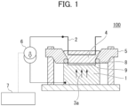
FIG. 1] FIG. 1 is a schematic diagram showing an example of a silicon carbide single crystal substrate treating system according to the present embodiment. - [
FIG. 2A] FIG. 2A is a schematic view of a silicon carbide single crystal substrate treating device used in Examples. - [
FIG. 2B] FIG. 2B is a top view of a cell of the silicon carbide single crystal substrate treating device used in Examples. - [
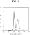
FIG. 3] FIG. 3 is an XPS spectrum of Si atoms (silicon atoms) of a SiC substrate subjected to an anodization treatment in Examples. - [
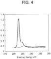
FIG. 4] FIG. 4 is an XPS spectrum of C atoms (carbon atoms) of a SiC substrate subjected to an anodization treatment in Example. - [
FIG. 5] FIG. 5 is an XPS spectrum of O atoms (oxygen atoms) of a SiC substrate subjected to an anodization treatment in Examples. - The method for treating a silicon carbide single crystal substrate according to the present embodiment includes a step (A) of forming an oxidized film on at least one main surface of the silicon carbide single crystal substrate by anodization using the silicon carbide single crystal substrate as an anode and by applying a voltage while bringing the at least one main surface of the silicon carbide single crystal substrate into contact with an electrolyte solution free of a fluorine anion. In the present embodiment, the "main surface" refers to a main surface of the substrate, and the substrate preferably has a first main surface and a second main surface (for example, a back surface). The present invention also relates to a method for forming an oxidized film including the method for treating a silicon carbide single crystal substrate according to the present embodiment, by including the step (A). The method for treating a silicon carbide single crystal substrate according to the present embodiment may further include a step (B) of etching the oxidized film by any of etching using at least one etchant selected from the group consisting of hydrofluoric acid and a mixture of hydrofluoric acid and ammonium fluoride, dry etching, ashing, or CMP. In the method for treating a silicon carbide single crystal substrate according to the present embodiment, the electrolyte solution does not contain fluorine anions, whereby it is possible to form an oxidized film on the silicon carbide single crystal substrate, the oxidized film allowing satisfactory removal not only by dry etching, ashing, or etching by CMP but also by wet etching using an etchant containing fluorine anions. Hereinafter, each step will be described.
- In the step (A), an oxidized film is formed on at least one main surface of a silicon carbide single crystal substrate (hereinafter also referred to as "SiC single crystal substrate") by anodization using the silicon carbide single crystal substrate as an anode and applying a voltage while contacting the silicon carbide single crystal substrate with an electrolyte solution free of a fluorine anion. Specifically, at least one main surface of the SiC single crystal substrate as an anode is brought into contact with an electrolyte solution free of a fluorine anion, and a surface (a surface other than a liquid contact surface) of the SiC single crystal substrate that is not in contact with the electrolyte solution and a cathode are electrically connected to each other with a DC power source device interposed therebetween. Then, a voltage is applied between the single crystal SiC substrate and the cathode by using a DC power source device, whereby an anodization treatment is performed across the entire main surface of the single crystal SiC substrate in an in-plane uniform manner to form an oxidized film on the main surface. The anodization treatment may be performed in an in-plane uniform manner across both the entire main surfaces of the SiC single crystal substrate, one side at a time.
- During the anodization treatment, the reactions occurring at the anode and cathode are presumed to be as follows.
- Anode: SiC + 4H2O → SiO2 + CO2 + 8H+ + 8e-
- Cathode: 8H+ + 8e- → 4H2
- Among the reaction products, carbon dioxide and hydrogen are desorbed as gas from the interface between the silicon carbide single crystal substrate and the electrolyte solution. On the other hand, silicon dioxide is formed on the surface of at least one main surface of the silicon carbide single crystal substrate as the reaction proceeds at the anode, and an oxidized film is formed on the at least one main surface.
- The SiC single crystal substrate in the step (A) is not particularly limited, and an industrially available SiC single crystal substrate may be used, or a SiC single crystal substrate having a silicon carbide semiconductor layer epitaxially grown on at least one main surface of the SiC substrate by a known method may be used. In the present embodiment, the SiC single crystal substrate may have a silicon carbide semiconductor layer epitaxially grown only on the first main surface, may have silicon carbide semiconductor layers epitaxially grown on both the first and second main surfaces, or may have no silicon carbide semiconductor layer epitaxially grown on either the first or second main surface.
- As the cathode in the step (A), a metal having a smaller ionization tendency than hydrogen can be used. Specifically, a metal such as copper, silver, palladium, platinum, or gold can be used as the cathode. Carbon that is stable in solutions can also be used as a cathode.
- In the step (A), the temperature of the electrolyte solution during the anodization is not particularly limited, but is preferably 300°C or less, more preferably 5 to 60°C, and still more preferably 10 to 40°C. When the treatment temperature of the anodization is within the above preferable range, a low boiling point solvent such as an aqueous solvent is easy to use, and the number of types of solvents that can be used is easy to increase. In addition, member selection of the device, safety measures and the like tend to be simple. In addition, it is easy to save power (cost) during manufacturing, and it is easy to shorten cooling time.
- In the step (A), the treatment time for anodization is not particularly limited, but is preferably 2 seconds to 30 minutes, more preferably 5 seconds to 20 minutes, and still more preferably 10 seconds to 10 minutes. When the treatment time of the anodization is within the above preferable range, it is easy to form an oxidized film having a desired film thickness on the first main surface with a high yield.
- In the step (A), the voltage to be applied for anodization is not particularly limited, but is preferably 1 to 60 V, more preferably 3 to 30 V, and still more preferably 5 to 20 V. When the applied voltage is within the above preferable range, it is easy to form an oxidized film having a desired film thickness on the first main surface.
- The electrolyte solution to be used in the step (A) is not particularly limited as long as it is free of a fluorine anion, but from the viewpoint of roughness, a stock solution of the electrolyte solution preferably has a viscosity of 1.0 mPa·s or more and 10 mPa·s or less at 20°C, and an aqueous solution preferably has a conductivity of 0.1 mS/cm or more and 900 mS/cm or less. Examples of the electrolyte solution include aqueous solutions containing any of the following components (E1) to (E4):
- component (E1): at least one selected from the group consisting of orthoperiodic acid, a periodate salt, iodic acid, and an iodate salt;
- component (E2): at least one selected from the group consisting of an acid free of a fluorine atom, a peracid free of a fluorine atom, and hydrogen peroxide;
- component (E3): an alkali free of a fluorine atom; and
- component (E4): an ammonium salt free of a fluorine atom.
- As the periodate salt of the component (E1), potassium periodate, sodium periodate, barium periodate, lithium periodate, and ammonium periodate are preferable, and sodium periodate is more preferable. As the iodate salt of the component (E1), orthoperiodic acid, sodium iodate, calcium iodate, or silver iodate is preferable. As the component (E1), orthoperiodic acid is preferable from the viewpoint of improving the pattern shape.
- As the component (E2), at least one selected from the group consisting of a carboxylic acid free of a fluorine atom, a percarboxylic acid free of a fluorine atom, a sulfonic acid free of a fluorine atom, a phosphonic acid free of a fluorine atom, an inorganic acid free of a fluorine atom, and hydrogen peroxide is preferable. As the carboxylic acid free of a fluorine atom, formic acid, citric acid, malonic acid, acetic acid, benzoic acid, lactic acid, malic acid, propionic acid, butyric acid, and valeric acid are preferable, and citric acid and acetic acid are more preferable. As the percarboxylic acid free of a fluorine atom, peracetic acid, perbenzoic acid, perlactic acid, performic acid, and perpropionic acid are preferable, and peracetic acid is more preferable. As the sulfonic acid free of a fluorine atom, sulfuric acid, methanesulfonic acid, ethanesulfonic acid, benzenesulfonic acid, and p-toluenesulfonic acid are preferable, and an aqueous solution of sulfuric acid or methanesulfonic acid is more preferable. As the phosphonic acid free of a fluorine atom, phosphoric acid, polyphosphoric acid, butylphosphonic acid, propylphosphonic acid, hexylphosphonic acid, and phenylphosphonic acid are preferable, and phosphoric acid and polyphosphoric acid are more preferable. As the inorganic acid free of a fluorine atom, sulfuric acid, phosphoric acid, polyphosphoric acid, nitric acid, nitrous acid, sulfurous acid, phosphorous acid, hydrochloric acid, chloric acid, and perchloric acid are preferable, and sulfuric acid, phosphoric acid, and nitric acid are more preferable.
- Among these, as the component (E2), citric acid, acetic acid, peracetic acid, sulfuric acid, phosphoric acid, nitric acid, and hydrogen peroxide are preferable, and sulfuric acid and phosphoric acid are more preferable.
- As the component (E3), at least one selected from the group consisting of a quaternary ammonium hydroxide salt free of a fluorine atom, a tertiary amine free of a fluorine atom, a secondary amine free of a fluorine atom, a primary amine free of a fluorine atom, and ammonia is preferable.
- Examples of the quaternary ammonium hydroxide salt free of a fluorine atom include tetraethylammonium hydroxide (TEAH), tetramethylammonium hydroxide (TMAH), tetrapropylammonium hydroxide (TPAH), dimethylbis(2-hydroxyethyl)ammonium hydroxide (DMEMAH), tetrabutylammonium hydroxide (TBAH), tetrapropylammonium hydroxide (TPAH), tris(2-hydroxyethyl)methylammonium hydroxide (THEMAH), choline, dimethyldiethylammonium hydroxide, tetraethanolammonium hydroxide, benzyltrimethylammonium hydroxide, benzyltriethylammonium hydroxide, benzyltributylammonium hydroxide are preferable, and tetramethylammonium hydroxide (TMAH) is more preferable.
- Examples of the tertiary amine free of a fluorine atom include alkylamines such as trimethylamine, triethylamine, tripropylamine, tributylamine, triisobutylamine, dimethylethylamine, dimethylpropylamine, allyldiethylamine, dimethyl-n-butylamine, and diethylisopropylamine; cycloalkylamines such as tricyclopentylamine and tricyclohexylamine and the like, 4-dimethylaminopyridine, N,N,N',N'-tetramethylethylenediamine, N,N,N',N'-tetraethylethylenediamine, N,N,N',N'-tetramethyl-1,3-diaminopropane, N,N,N',N'-tetramethyl-1,3-diaminobutane, N',N'-tetramethyl-1,4-diaminobutane, N,N,N',N'-tetramethylphenylenediamine, 1,2-dipiperidinoethane, N-methylpiperidine, N-methylpyrrolidine, and N-methylmorpholine are preferable, and tributylamine is more preferable.
- Examples of the preferable secondary amine free of a fluorine atom include alkylamines such as dimethylamine, diethylamine, methylethylamine, dipropylamine, diisopropylamine, dibutylamine, diisobutylamine, and butylmethylamine; cycloalkylamines such as N,N-dicyclohexylamine, N-cyclopentylcyclohexanamine; alkoxyamines such as methoxy(methylamine) and N-(2-methoxyethyl)ethylamine; piperidine, 2-pipecolin, 3-pipecolin, 4-pipecolin, 2,6-dimethylpiperidine, 3,5-dimethylpiperidine, pyrrolidine, 2-methylpyrrolidine, 3-methylpyrrolidine, morpholine, 2-methylmorpholine, 3-methylmorpholine, 2-methylpiperazine, 2,3-dimethylpiperazine, 2,5-dimethylpiperazine, N,N'-dimethylethanediamine, N,N'-dimethylpropanediamine, N,N'-diethylethylenediamine, N,N'-diethylpropanediamine, and N,N'-diisopropylethylenediamine and dibutylamine is more preferable.
- Examples of preferable primary amine free of a fluorine atom include alkylamines such as methylamine, ethylamine, propylamine, n-butylamine, isopropylamine, and tert-butylamine; cycloalkylamines such as cyclopentylamine, cyclohexylamine, and cyclohexanemethylamine; alkoxyamines such as methoxyethylamine, methoxypropylamine, methoxybutylamine, ethoxypropylamine, and propoxypropylamine, other hydroxylamines, 2-(2-aminoethylamino)ethanol, ethylenediamine,
butane 1,4-diamine, 1,3-propanediamine, 1,6-hexanediamine, pentane-1,5-diamine, and monoethanolamine, and n-butylamine and monoethanolamine are more preferable. - Examples of the component (E3) include alkali metal salts such as potassium chloride. Among them, monoethanolamine and TMAH are preferable as the component (E3).
- As the component (E4), an ammonium salt of an organic carboxylic acid is preferable, and triammonium citrate, ammonium acetate, triammonium citrate, ammonium acetate, ammonium propionate, ammonium butyrate, and ammonium oxalate are more preferable. Among them, triammonium citrate and ammonium acetate are preferable as the component (E4).
- The electrolyte solution may be used alone or in combination of two or more types thereof. Among them, as the electrolyte solution, the component (E1) or a combination of the component (E1) and at least one of the components (E2) to (E4) is preferable, and orthoperiodic acid or a combination of orthoperiodic acid and at least one of the components (E2) to (E4) is more preferable, from the viewpoint of forming an oxidized film having a desired film thickness at a low voltage in a short time.
- The concentration of the electrolyte solution is not particularly limited as long as it is an aqueous solution containing any of the components (E1) to (E4), but is preferably 0.0001 to 99.99% by mass, more preferably 0.001 to 90% by mass, and still more preferably 0.002 to 50% by mass. The electrolyte solution (aqueous solution) having a concentration within the above preferable range is easy to form an oxidized film having a desired film thickness on the main surface of the single crystal SiC substrate.
- In the present embodiment, the electrolyte solution may contain at least one antifoaming agent selected from the group consisting of an organic solvent and a surfactant.
- The organic solvent is preferably an alcohol solvent. Examples of the alcohol solvent include alcohols (monohydric alcohols) such as ethanol, 1-propanol, isopropanol, 1-butanol, 2-butanol, isobutanol, 3-methyl-1-butanol, tert-butyl alcohol, 1-pentanol, 2-pentanol, 1-hexanol, 1-heptanol, 1-octanol, 1-decanol, 2-hexanol, 2-heptanol, 2-octanol, 3-hexanol, 3-heptanol, 3-octanol, 4-octanol, 3-methyl-3-pentanol, cyclopentanol, 2,3-dimethyl-2-butanol, 3,3-dimethyl-2-butanol, 2-methyl-2-pentanol, 2-methyl-3-pentanol, 3-methyl-2-pentanol, 3-methyl-3-pentanol, 4-methyl-2-pentanol, 4-methyl-3-pentanol, cyclohexanol, 5-methyl-2-hexanol, 4-methyl-2-hexanol, 4,5-dimethyl-2-hexanol, 6-methyl-2-heptanol, 7-methyl-2-octanol, 8-methyl-2-nonal, 9-methyl-2-decanol, 3-methoxy-1-butanol, and 3-methoxy-3-methyl-1-butanol; glycol-based solvents such as ethylene glycol, diethylene glycol, propylene glycol and triethylene glycol; polyhydric alcohol solvents such as glycerin; glycol ether solvents containing a hydroxyl group such as ethylene glycol monomethyl ether, propylene glycol monomethyl ether (PGME; also known as 1-methoxy-2-propanol), diethylene glycol monomethyl ether, triethylene glycol monoethyl ether, methoxymethyl butanol, ethylene glycol monoethyl ether, ethylene glycol monopropyl ether, ethylene glycol monobutyl ether, propylene glycol monoethyl ether, propylene glycol monopropyl ether, propylene glycol monobutyl ether, propylene glycol monophenyl ether, and dipropylene glycol dimethyl ether.
- Examples of the organic solvent other than the alcohol solvent include propylene glycol monomethyl ether acetate (PEGEMA), acetic acid, ethyl acetate, propyl acetate, isopropyl acetate, butyl acetate, cyclohexanone, DMAC, DMSO, NMP, 2-pyrrolidone, sulfolane, propylene carbonate, acetone, cyclohexanone, and N-methylmorpholine-N-oxide.
- Examples of the surfactant include a nonionic surfactant, an anionic surfactant, a cationic surfactant, and an amphoteric surfactant.
- Examples of the nonionic surfactant include a polyalkylene oxide alkylphenyl ether-based surfactant, a polyalkylene oxide alkyl ether-based surfactant, a block polymer-based surfactant consisting of polyethylene oxide and polypropylene oxide, a polyoxyalkylene distyrened phenyl ether-based surfactant, a polyalkylene tribenzylphenyl ether-based surfactant, and an acetylene polyalkylene oxide-based surfactant.
- Examples of the anionic surfactant include alkyl sulfonic acid, alkyl benzene sulfonic acid, alkyl naphthalene sulfonic acid, alkyl diphenyl ether sulfonic acid, fatty acid amide sulfonic acid, polyoxyethylene alkyl ether carboxylic acid, polyoxyethylene alkyl ether acetic acid, polyoxyethylene alkyl ether propionic acid, alkyl phosphonic acid, and salts of fatty acids. Examples of the "salt" include an ammonium salt, a sodium salt, a potassium salt, and a tetramethylammonium salt.
- Examples of the cationic surfactant include alkylpyridium-based surfactants and quaternary ammonium salt-based surfactants.
- Examples of the amphoteric surfactant include a betaine surfactant, an amino acid surfactant, an imidazoline surfactant, and an amine oxide surfactant.
- The antifoaming agents may be used alone or in combination of two or more types thereof. The content of the antifoaming agent is not particularly limited, but is preferably 0.0001% by mass to 50% by mass, more preferably 0.0002% by mass to 10% by mass, still more preferably 0.002% by mass to 1% by mass, and particularly preferably 0.002% by mass to 0.2% by mass based on the total amount of the electrolyte solution. When the content of the antifoaming agent is within the above preferable range, it is easy to prevent bubble formation on the surface of the SiC single crystal substrate after anodization. Thus, an oxidized film having a desired film thickness can be easily formed in an in-plane uniform manner across the main surface.
- In the present embodiment, the electrolyte solution preferably has a final current density of 0.01 mA/cm2 or more, more preferably 0.1 mA/cm2 or more, and still more preferably 0.3 mA/cm2 or more, the final current density being a current density a variation width of which is in a range of ±3 mA/cm2 continuously for 60 seconds after the voltage is applied in the step (A). The upper limit of the final current density is not particularly limited, and examples thereof include 20 mA/cm2 or less, 15 mA/cm2 or less, and 12 mA/cm2 or less. When the final current density is within the above preferable range, the formation of an oxidized film more preferentially occurs than the oxidation reaction of the electrolyte solution.
- The thickness of the oxidized film formed in the step (A) is not particularly limited, and can be appropriately adjusted according to the purpose. In the present embodiment, for example, an oxidized film having a film thickness of 1 to 2,000 nm can be formed. The thickness of the oxidized film is preferably 10 to 1,800 nm, and more preferably 20 to 1,500 nm.
- In the step (B), the oxidized film formed in the step (A) is removed by any one of etching (hereinafter simply referred to as "wet etching") using at least one etchant selected from the group consisting of hydrofluoric acid and a mixture of hydrofluoric acid and ammonium fluoride, dry etching, ashing, and CMP (chemical mechanical polishing). According to the present invention, it is possible to form, on a silicon carbide single crystal substrate, an oxidized film that can be satisfactorily removed not only by dry etching, ashing, or CMP but also by wet etching using an etchant containing a fluorine anion. Treatment conditions for removal are not particularly limited, and known treatment conditions can be employed.
- In the case of dry etching or ashing in the step (B), it is preferable to perform the etching treatment with a gas containing halogen atoms from the viewpoint of performing an etching treatment more efficiently. Examples of a gas containing a fluorine atom include CF4, CHF3, and SF6 gas. Examples of a gas containing a chlorine atom include Cl2 gas and BCl3 gas.
- The method for treating a SiC single crystal substrate according to the present embodiment may or may not include a step (C) of replenishing the electrolyte solution with a replenishing liquid having a higher electrolyte concentration than the electrolyte solution. In the step (C), the electrolyte solution may be replenished with a replenishing liquid having a higher electrolyte concentration than the electrolyte solution. The timing of performing the step (C) is not particularly limited, but when the concentration of the electrolyte solution becomes lower than before the anodization is started, the replenishing liquid may be added to the electrolyte solution. For example, when the electrolyte is an acid, the concentration of hydrogen ions in the replenishing liquid is made higher than that in the electrolyte solution. Further, when the electrolyte is an alkali, the concentration of hydroxide ions in the replenishing liquid is made higher than the concentration in the electrolyte solution. In the present embodiment, it is preferable to add the replenishing liquid to the electrolyte solution when the electrolyte concentration of the electrolyte solution becomes 3% or more lower than that before the start of anodization.
- According to the method for treating a SiC single crystal substrate of the present embodiment, it is possible to control film thickness of a desired surface of a SiC single crystal substrate in a short time under mild conditions such as room temperature. In addition, in the method for treating a SiC single crystal substrate according to the present embodiment, a metal-free high-purity solution having high stability that can be used in semiconductors can be used. In addition, an oxidized film having a desired film thickness can be formed in an in-plane uniform manner across the SiC surface, and by etching the oxidized film, it is possible to etch the SiC substrate while maintaining a smooth surface. In addition, the method for treating a SiC single crystal substrate of the present embodiment can eliminate a treatment such as light irradiation during the anodization, it is possible to simplify manufacturing equipment. Therefore, according to the method for treating a SiC single crystal substrate of the present embodiment, it is possible to decrease cost of the entire manufacturing process and increase the yield.
- A silicon carbide single-crystal substrate treating system according to the present embodiment includes an anode that is a silicon carbide single crystal substrate; a cathode opposed to the silicon carbide single crystal substrate; an electrolyte solution interposed between the silicon carbide single crystal substrate and the cathode, being in contact with the anode and the cathode, and being free of a fluorine anion; and a power source device connected between the anode and the cathode and causing anodization at an interface of at least one main surface of the anode by application of a voltage.
- Hereinafter, the silicon carbide single crystal substrate treating system according to the present embodiment will be described with reference to the drawings.
FIG. 1 is a schematic diagram showing an example of the silicon carbide single crystal substrate treating system according to the present embodiment. A silicon carbide single crystalsubstrate treating system 100 includes anelectrolysis bath 5 containing anelectrolyte solution 4, apower source 6 and apower source controller 7, a cathode (silver, palladium, platinum, gold, carbon, etc.) 2 connected to the power source and aworkpiece 1 to be subjected to anodization as an anode (in this case, the SiC single crystal substrate is an anode 1) connected to the power source, and theelectrolyte solution 4 interposed between theanode 1 and thecathode 2. In the case of this example, aseal 8 is provided between theelectrolysis bath 5 and theanode 1 so that theelectrolyte solution 4 does not leak out, but this is for preventing theelectrolyte solution 4 from being brought into contact with a surface other than the surface to be treated of theanode 1, and theseal 8 is not always necessary depending on the device configuration. When a current flows through the SiC single crystal substrate (anode 1) and thecathode 2 via thepower source controller 7, a current 3a flows toward the substrate surface to cause an anodization reaction, regardless of whether the SiC single crystal substrate is a p-type or n-type substrate. Anoxidized film 9 is formed on the SiC single crystal substrate by the anodization reaction. - In the present embodiment, the SiC single crystal substrate (anode 1) is the same as the SiC single crystal substrate in the method for treating a silicon carbide single crystal substrate described above.
- In the present embodiment, the
electrolyte solution 4 is free of a fluorine anion, and is the same as the electrolyte solution in the above-described method for treating a silicon carbide single crystal substrate. The concentration of theelectrolyte solution 4 may be adjusted immediately before theelectrolyte solution 4 is brought into contact with the SiC single crystal substrate (anode 1), or theelectrolyte solution 4 may be used by adding a chemical solution having a high concentration. Further, even when theelectrolyte solution 4 contains impurities such as a substance eluted from the SiC single crystal substrate, with which theelectrolyte solution 4 had come into contact, theelectrolyte solution 4 may be used as it is, or the impurities may be removed in the circulation process. When the electrolyte solution is used by adding a chemical solution having a high concentration, the replenishment is carried out using a replenishing liquid, which has an electrolyte concentration higher than the electrolyte solution. For example, when the electrolyte is an acid, the concentration of hydrogen ions in the replenishing liquid should be set higher than the concentration in the electrolyte solution. When the electrolyte is an alkali, the concentration of hydroxide ions in the replenishing liquid should be set higher than the concentration in the electrolyte solution. - In the present embodiment, treatment conditions for the anodization are the same as those for the anodization in the above-described method for treating a silicon carbide single crystal substrate.
- According to the silicon carbide single crystal substrate treating system of the present embodiment, it is possible to control film thickness of a desired surface of a SiC single crystal substrate in a short time under mild conditions such as room temperature. In addition, in the silicon carbide single crystal substrate treating system according to the present embodiment, a metal-free high-purity solution having high stability that can be used in semiconductors can be used. Further, the silicon carbide single crystal substrate treating system of the present embodiment can eliminate a treatment such as light irradiation during the anodization, it is possible to simplify manufacturing equipment. Therefore, according to the silicon carbide single crystal substrate treating system of the present embodiment, it is possible to decrease cost of the entire manufacturing process and increase the yield. In addition, the SiC single crystal substrate obtained by the silicon carbide single crystal substrate treating system according to the present embodiment can be subjected to a high accuracy processing treatment of the oxidized film by the etching of the step (B) in the above-described silicon carbide single crystal substrate treating method.
- The embodiment shown in
FIG. 1 is explained by exemplifying the configuration in which the anodization is carried out by horizontally disposing the SiC single crystal substrate (anode 1) on the bottom surface of theelectrolysis bath 5, but the silicon carbide single crystal substrate treating system according to the present embodiment is not limited thereto. For example, in a case where a plurality of SiC single crystal substrates are subjected to the anodization treatment at the same time, the anodization treatment may be carried out by providing a substrate holding mechanism, while holding the SiC single crystal substrates so that only a surface to be treated of each SiC single crystal substrate comes into contact with theelectrolyte solution 4. In another possible configuration, the anodization treatment may be performed, by disposing the SiC single crystal substrate perpendicular to the bottom surface of theelectrolysis bath 5. - Hereinafter, the present invention will be described in more detail with reference to Examples, but will not be limited thereto.
- In each Test Example, aqueous electrolyte solutions having compositions shown in Table 1 were prepared.
- In potentiostat R600+ (manufactured by GAMRY), a SiC wafer (having a silicon carbide semiconductor layer epitaxially grown on the first main surface, manufactured by Showa Denko) was used as an anode (21), an Ag/AgCl electrode was used as a reference electrode (22), and a Pt electrode was used as a negative electrode (23) (
FIG. 2A ). 1 ml of an electrolyte solution (24) of each Test Example was added to a cell (25) with a radius of 4 mm as shown inFIG. 2B . Then, a voltage shown in Table 1 was applied to a wetted part and/or a voltage application unit (A) at room temperature (23°C) for a treatment time shown in Table 1 using chronocoulometry to perform anodization of the SiC. The thickness (nm) of an oxidized film (SiO2 film) formed by the voltage application was observed by X-SEM along a portion (B) wetted with the electrolyte. Thereafter, the SiC substrate on which the oxidized film had been formed was immersed in a 5% HF (hydrofluoric acid) solution in a beaker for 10 minutes to remove the oxidized film, and cross-sectional observation was performed by X-SEM. A substrate from which the oxidized film had been removed was evaluated as "O" (good), and a substrate from which the oxidized film had not been removed was evaluated as "X" (poor). The results are shown in Table 1. In each Test Example, the maximum current density (mA/cm2) in the voltage application treatment and the final current density (mA/cm2) were measured, where the final current density is a current density, a variation width of which is in a range of ±3 mA/cm2 continuously for 60 seconds after the voltage is applied. The results are shown in Table 1. In Table 1 below, "%" indicates "% by mass". The same applies to Tables 2 and 3 described below.[Table 1] Test Example Electrolyte solution Voltage application SiO2 film formed by anodization Oxidized film removal evaluation Maximum current density (mA/cm2 ) Final current density (mA/cm2) Voltage (V) Treatment time (min) 1 0.001%H5IO6 7 3 300 ○ 0.562 0.188 2 0.01%H5IO6 7 3 300 ○ 2.68 0.64 3 1% H5IO6 7 1 100 ○ 176 1.32 4 1% H5IO6 7 3 300 ○ 62.36 0.88 5 1% H5IO6 7 10 300 ○ 2.048 0.2798 6 1% H5IO6 4 3 100 ○ 17.2 0.4 7 1% H5IO6 5 3 300 ○ 2.45 0.42 8 1% H5IO6 10 3 600 ○ 80.49 0.88 9 20% H5IO6 7 3 230 ○ 2.048 0.86 10 1% HIO3 7 3 300 ○ 2.26 0.84 11 1% H2SO4 7 3 240 ○ 3.266 0.832 12 1% H3PO4 7 3 240 ○ 2.306 0.768 13 1% Citric acid 7 3 300 ○ 1.473 0.946 14 1% Acetic acid 7 3 300 ○ 1.472 0.94 15 1% Peracetic acid 7 3 200 ○ 1.21 0.65 16 1% H2O2 7 3 210 ○ 52.47 0.97 17 1% HNO3 7 3 240 ○ 222.53 0.44 18 1% NH4OH 7 3 240 ○ 18.05 0.80 19 1% TMAH 7 3 150 ○ 165.21 0.66 20 1% n-butylamine 7 3 200 ○ 2.146 0.555 21 1% Dibutylamine 7 3 200 ○ 3.13 0.47 22 1% Tributylamine 7 3 200 ○ 2.68 0.55 23 1% Monoethanolamine 7 3 200 ○ 1.46 0.622 24 1% Triammonium citrate 7 3 230 ○ 59.71 0.88 25 1% Ammonium acetate 7 3 240 ○ 36.82 0.84 26 1% H5IO6+1%Acetic acid 7 3 100 ○ 1.946 0.886 27 1% H5IO6+10%Acetic acid 7 3 230 ○ 40.25 0.80 28 1% H5IO6+1% H2SO4 7 3 230 ○ 12.42 0.714 29 1% NaOI4 7 3 200 ○ 1.98 0.794 30 7.4%KCI(0.1mol/I) 7 3 300 ○ 2.378 0.7512 31 1%HF 7 3 840 × 131.37 11.06 32 1%NH4F 7 3 880 × 39.03 8.07 33 1% H5IO6 +200ppmSurfactant 7 3 300 ○ 25.42 0.92 34 1% H5IO6 +50%Acetic acid 7 3 300 ○ 27.86 8.666 35 1% H2O2 +200ppmSurfactant 7 3 210 ○ 28.34 0.83 36 1% H2O2 +10%Glycerin 7 3 150 ○ 28.41 0.86 37 3%Citric acid 9 3 250 ○ 3.556 1.577 38 30%Citric acid 9 3 260 ○ 10.222 0.835 39 100ppmSulfuric acid 9 3 160 ○ 10.77 2.222 40 0.1%Sulfuric acid 9 3 530 ○ 49.34 2.222 41 1%Sulfuric acid 9 3 490 ○ 275.6 4.444 42 20%Sulfuric acid 9 3 490 ○ 10013.4 3.668 43 20%Sulfuric acid 9 10 1200 ○ 131.12 1.5996 44 20%Methanesulfonic acid 9 3 240 ○ 252 2.306 45 1%Phosphoric acid 9 3 680 ○ 65.78 2.444 46 20%Phosphoric acid 9 3 290 ○ 243.2 5.546 47 20%Polyphosphoric acid 9 3 280 ○ 218.28 5.22 - As is clear from the results shown in Table 1, in each of Test Examples 1 to 47, an oxidized film could be formed on a desired surface of the silicon carbide single crystal substrate in a short time under mild conditions such as room temperature. It can be said that both oxidized films formed in Test Examples 31 and 32 containing fluorine anions in the electrolyte solution were poor in etching removability.
- An anodization treatment of SiC substrates was performed by using a 1% H5IO6 electrolyte solution in the same manner as in [Treatment (1) of SiC Substrate: Formation of Oxidized Film by Anodization] described above. Thereafter, the SiC substrate on which the oxidized film had been formed was treated under the conditions shown in Table 2 to remove the oxidized films. Cross-section observation was performed by X-SEM, and a sample from which the oxidized film had been removed was evaluated as "O" (good), and a sample from which the oxidized film had not been removed was evaluated as "X" (poor). The results are shown in Table 2.
[Table 2] Conditions for oxidized film removal treatment Oxidized film removal evaluation Treatment method Treatment conditions Treatment temperature (°C) Treatment time (min) Device Wet etching 5 %HF 23 10 Beaker evaluation ○ BHF (1%HF+20%NH4F) 23 10 Beaker evaluation ○ Dry etching CF4/O2=90/10sccm, RF=1200W, Bias 200W 23 3 Evaluation device for experiments ○ Ashing CF4/O2=50/100sccm, RF=600W 80 3 TCA3822 (manufactured by Tokyo Ohka Kogyo) ○ - As is clear from the results shown in Table 2, it can be seen that each oxidized film formed on the SiC substrate by the method of the present invention could be satisfactorily removed by any of wet etching, dry etching, or ashing.
- Similarly to [Treatment (1) of SiC Substrate: Formation of Oxidized Film by Anodization] described above, a SiC wafer (having a silicon carbide semiconductor layer epitaxially grown on the first main surface, manufactured by Showa Denko) was used as an anode, an Ag/AgCl electrode was used as a reference electrode, and a Pt electrode was used as a negative electrode. The electrolyte solutions of Test Examples 4, 16, 33, 34, 35 or 36 were each placed in a beaker, and the SiC substrate was subjected to an anodization treatment at room temperature (23°C) under conditions of a voltage of 7 V and a treatment time of 3 minutes. After the anodization treatment, the presence or absence of bubble formation on each SiC substrate was visually evaluated, and a sample without bubble formation was evaluated as "O" (good), and a sample with bubble formation was evaluated as "X" (poor). The results are shown in Table 3.
[Table 3] Test Example Electrolyte solution Voltage application Foaming evaluation Oxidized film removal evaluation Voltage (V) Treatment time (min) 4 1% H5IO6 7 3 × ○ 16 1% H2O2 7 3 × ○ 33 1% H5IO6 + 200ppmSurfactant 7 3 ○ ○ 34 1% H5IO6 +50% Acetic acid 7 3 ○ ○ 35 1% H2O2 + 200ppmSurfactant 7 3 ○ ○ 36 1% H2O2 +10 %Glycerin 7 3 ○ ○ - As is clear from the results shown in Table 3, bubble formation occurred in Test Examples 4 and 16 in which the electrolyte solution did not contain an antifoaming agent. On the other hand, in Test Examples 33 to 36 in which the electrolyte solution contained an antifoaming agent, bubble formation could be suppressed.
- A SiC wafer as an anode and Pt as a cathode were immersed in a 1% periodic acid (H5IO6) solution, and a voltage of 7 V was applied at room temperature for 3 minutes. Subsequently, the SiC wafer was washed with water for 30 seconds in a beaker and dried by a N2 blow, and then the surface of the SiC wafer was subjected to XPS measurement using K-Alpha (manufactured by Thermo Scientific). The results of qualitative analysis by the XPS measurement are shown in Table 4. XPS spectra of Si, C and O are shown in
FIGs. 3 to 5 . - A SiC wafer as an anode and Pt as a cathode were immersed in a 1% periodic acid (H5IO6) solution, and a voltage of 7 V was applied at room temperature for 3 minutes. Subsequently, the SiC wafer was washed with water in a beaker for 30 seconds, and then immersed in 5% HF at room temperature for 10 minutes to remove the oxidized film. After the oxidized film removal treatment, the SiC wafer was washed with water for 30 seconds in a beaker and dried by a N2 blow, and then the surface of the SiC wafer was subjected to XPS measurement using K-Alpha (manufactured by Thermo Scientific). The results of qualitative analysis by the XPS measurement are shown in Table 4. XPS spectra of Si, C and O are shown in
FIGs. 3 to 5 .[Table 4] Si(%) C(%) O(%) Ref(Untreated) 49.2 49.2 1.6 Test Example48 33.5 1.0 65.5 Test Example49 49.4 49.4 1.2 - As is clear from the results shown in Table 4 and
FIGs. 3 to 5 , it can be seen that an oxidized film was formed in Test Example 48. In addition, since the component ratios of Test Example 49, which had been subjected to the porous film removal treatment, were the same as Si, C, and O component ratios of an untreated SiC substrate, it can be seen that the oxidized film had been removed. -
- 1 Anode
- 2 Cathode
- 4 Electrolyte solution
- 5 Electrolysis bath
- 6 Power source
- 7 Power source controller
- 8 Seal
- 9 Oxidized film
- 100 Silicon carbide single crystal substrate treating system
Claims (17)
- A method for treating a silicon carbide single crystal substrate, comprising: a step (A) of forming an oxidized film on at least one main surface of the silicon carbide single crystal substrate by anodization using the silicon carbide single crystal substrate as an anode and applying a voltage while bringing the at least one main surface of the silicon carbide single crystal substrate into contact with an electrolyte solution free of a fluorine anion.
- The method for treating a silicon carbide single crystal substrate according to claim 1, wherein the electrolyte solution has a final current density of 0.01 mA/cm2 or more, the final current density being a current density, a variation width of which is in a range of ±3 mA/cm2 continuously for 60 seconds after the voltage is applied in the step (A).
- The method for treating a silicon carbide single crystal substrate according to claim 1, further comprising a step (B) of removing the oxidized film by any of etching using at least one etchant selected from the group consisting of hydrofluoric acid and a mixture of hydrofluoric acid and ammonium fluoride, dry etching, ashing, or CMP.
- The method for treating a silicon carbide single crystal substrate according to claim 3, wherein the dry etching or the ashing comprises etching with a gas comprising a halogen atom.
- The method for treating a silicon carbide single crystal substrate according to claim 1, wherein the electrolyte solution comprises at least one selected from the group consisting of orthoperiodic acid, a periodate salt, iodic acid, and an iodate salt.
- The method for treating a silicon carbide single crystal substrate according to claim 1, wherein the electrolyte solution comprises at least one selected from the group consisting of an acid free of a fluorine atom, a peracid free of a fluorine atom, and hydrogen peroxide.
- The method for treating a silicon carbide single crystal substrate according to claim 6, wherein the electrolyte solution is at least one selected from the group consisting of a carboxylic acid free of a fluorine atom, a percarboxylic acid free of a fluorine atom, a sulfonic acid free of a fluorine atom, a phosphonic acid free of a fluorine atom, an inorganic acid free of a fluorine atom, and hydrogen peroxide.
- The method for treating a silicon carbide single crystal substrate according to claim 7, wherein the sulfonic acid free of a fluorine atom comprises at least one selected from the group consisting of sulfuric acid and methanesulfonic acid.
- The method for treating a silicon carbide single crystal substrate according to claim 7, wherein the phosphonic acid free of a fluorine atom comprises at least one selected from the group consisting of phosphoric acid and polyphosphoric acid.
- The method for treating a silicon carbide single crystal substrate according to claim 1, wherein the electrolyte solution comprises an alkali free of a fluorine atom.
- The method for treating a silicon carbide single crystal substrate according to claim 10, wherein the alkali is at least one selected from the group consisting of a quaternary ammonium hydroxide salt free of a fluorine atom, a tertiary amine free of a fluorine atom, a secondary amine free of a fluorine atom, a primary amine free of a fluorine atom, and ammonia.
- The method for treating a silicon carbide single crystal substrate according to claim 1, wherein the electrolyte solution comprises an ammonium salt free of a fluorine atom.
- The method for treating a silicon carbide single crystal substrate according to claim 1, wherein the electrolyte solution comprises at least one antifoaming agent selected from the group consisting of an organic solvent and a surfactant.
- The method for treating a silicon carbide single crystal substrate according to claim 13, wherein the antifoaming agent comprises an alcohol solvent.
- The method for treating a silicon carbide single crystal substrate according to any one of claims 1 to 12, wherein the step (A) is performed at a liquid temperature of the electrolyte solution of 300°C or less.
- A silicon carbide single crystal substrate treating system comprising:an anode that is a silicon carbide single crystal substrate;a cathode opposed to the silicon carbide single crystal substrate;an electrolyte solution interposed between the silicon carbide single crystal substrate and the cathode, being in contact with the anode and the cathode, and being free of a fluorine anion; anda power source device connected between the anode and the cathode and causing anodization at an interface of at least one main surface of the anode by application of a voltage.
- A replenishing liquid for replenishing the electrolyte solution for use in the method for treating a silicon carbide single crystal substrate according to claim 1, wherein the replenishing liquid has a higher electrolyte concentration than the electrolyte solution.
Applications Claiming Priority (2)
| Application Number | Priority Date | Filing Date | Title |
|---|---|---|---|
| JP2022106470 | 2022-06-30 | ||
| PCT/JP2023/023362 WO2024004864A1 (en) | 2022-06-30 | 2023-06-23 | Silicon carbide single crystal substrate processing method, and silicon carbide single crystal substrate processing system |
Publications (2)
| Publication Number | Publication Date |
|---|---|
| EP4539105A1 true EP4539105A1 (en) | 2025-04-16 |
| EP4539105A4 EP4539105A4 (en) | 2025-10-29 |
Family
ID=89382971
Family Applications (1)
| Application Number | Title | Priority Date | Filing Date |
|---|---|---|---|
| EP23831306.8A Pending EP4539105A4 (en) | 2022-06-30 | 2023-06-23 | METHOD FOR PROCESSING A SILICIUM CARBIDE SINGLE CRYSTAL SUBSTRATE AND SYSTEM FOR PROCESSING A SILICIUM CARBIDE SINGLE CRYSTAL SUBSTRATE |
Country Status (5)
| Country | Link |
|---|---|
| US (1) | US20250382724A1 (en) |
| EP (1) | EP4539105A4 (en) |
| JP (1) | JPWO2024004864A1 (en) |
| KR (1) | KR20250026771A (en) |
| WO (1) | WO2024004864A1 (en) |
Family Cites Families (12)
| Publication number | Priority date | Publication date | Assignee | Title |
|---|---|---|---|---|
| JPS586294Y2 (en) | 1978-10-20 | 1983-02-03 | ダイワ精工株式会社 | Braking device for spinning reel |
| JPH06104436A (en) * | 1992-09-18 | 1994-04-15 | Fujitsu Ltd | Method of manufacturing thin film transistor |
| JP2934115B2 (en) * | 1993-03-03 | 1999-08-16 | シャープ株式会社 | Thin film element and method of manufacturing the same |
| JP2003133308A (en) * | 2001-10-23 | 2003-05-09 | Nagoya Industrial Science Research Inst | Method for manufacturing oxide film of silicon carbide, apparatus for manufacturing oxide film, and method for manufacturing semiconductor element using oxide film |
| JP5035796B2 (en) * | 2007-07-09 | 2012-09-26 | 東海カーボン株式会社 | Cleaning method of plasma etching electrode plate |
| JP5560774B2 (en) | 2010-03-03 | 2014-07-30 | 日立金属株式会社 | Method for manufacturing silicon carbide single crystal substrate |
| JP6143283B2 (en) * | 2013-03-22 | 2017-06-07 | 国立大学法人大阪大学 | Shape creation etching method and high precision shape creation method using anodization |
| US9472395B2 (en) * | 2015-01-12 | 2016-10-18 | Infineon Technologies Ag | Semiconductor arrangement including buried anodic oxide and manufacturing method |
| JP6821948B2 (en) | 2016-05-23 | 2021-01-27 | 株式会社豊田中央研究所 | Etching Solution, Etching Equipment, and Etching Method Used for Photoelectrochemical Etching of Silicon Carbide (SiC) Substrate |
| JP7628677B2 (en) * | 2019-08-05 | 2025-02-12 | 国立大学法人大阪大学 | Anodizing-assisted polishing method |
| JP7226200B2 (en) | 2019-09-06 | 2023-02-21 | 株式会社デンソー | Etching solution and etching method |
| JP7670277B2 (en) * | 2019-11-18 | 2025-04-30 | 富士電機株式会社 | Silicon carbide semiconductor device and method for manufacturing silicon carbide semiconductor device |
-
2023
- 2023-06-23 KR KR1020247041840A patent/KR20250026771A/en active Pending
- 2023-06-23 WO PCT/JP2023/023362 patent/WO2024004864A1/en not_active Ceased
- 2023-06-23 JP JP2024530775A patent/JPWO2024004864A1/ja active Pending
- 2023-06-23 EP EP23831306.8A patent/EP4539105A4/en active Pending
- 2023-06-23 US US18/874,924 patent/US20250382724A1/en active Pending
Also Published As
| Publication number | Publication date |
|---|---|
| WO2024004864A1 (en) | 2024-01-04 |
| US20250382724A1 (en) | 2025-12-18 |
| KR20250026771A (en) | 2025-02-25 |
| JPWO2024004864A1 (en) | 2024-01-04 |
| EP4539105A4 (en) | 2025-10-29 |
Similar Documents
| Publication | Publication Date | Title |
|---|---|---|
| CN110777381B (en) | Composition for TiN hardmask removal and etch residue cleaning | |
| EP2798669B1 (en) | Compositions and methods for selectively etching titanium nitride | |
| EP1988567B1 (en) | Method for reducing microroughness of semiconductor surface | |
| US9678430B2 (en) | Composition and process for stripping photoresist from a surface including titanium nitride | |
| US9222018B1 (en) | Titanium nitride hard mask and etch residue removal | |
| AU2024205104B2 (en) | Branched amino acid surfactants for electronics products | |
| CN115044375A (en) | Etching composition | |
| US6802911B2 (en) | Method for cleaning damaged layers and polymer residue from semiconductor device | |
| CN109423290B (en) | Etching solution for selectively removing tantalum nitride relative to titanium nitride in manufacturing semiconductor device | |
| JP2015122496A (en) | Composition for titanium nitride hard mask and removal of etching residue | |
| JP3679216B2 (en) | Semiconductor substrate cleaning liquid and cleaning method using the same | |
| US20120273010A1 (en) | Composition and Method to Remove Excess Material During Manufacturing of Semiconductor Devices | |
| KR20050085663A (en) | Methods for polishing and/or cleaning copper interconnects and/or film and compositions therefor | |
| EP2437284A2 (en) | Cleaning agent for semiconductor substrate, cleaning method using the cleaning agent, and method for producing semiconductor element | |
| JP2014057039A (en) | Process of manufacturing semiconductor substrate product and etchant | |
| CN101313391A (en) | Semiconductor surface treating agent | |
| JP5548224B2 (en) | Semiconductor substrate product manufacturing method and etching solution | |
| US20250382724A1 (en) | Silicon carbide single crystal substrate processing method, and silicon carbide single crystal substrate processing system | |
| EP4539106A1 (en) | Processing method for silicon carbide single crystal substrate, silicon carbide single crystal substrate processing system, and replenishing liquid | |
| KR102397090B1 (en) | Composition for removal of Ni and TiN | |
| TWI415184B (en) | Method for thinning and homogenizing a thickness of a semiconductor layer on a surface of an electrically insulating material | |
| JP3751255B2 (en) | Insulating film etchant | |
| TWI532834B (en) | Method for cleaning semiconductor substrate and detergent for two-component semiconductor substrate | |
| TW201938480A (en) | Protective fluid for alumina, protection method, and production method for semiconductor substrate having alumina layer using same | |
| KR102092352B1 (en) | Manufacturing method of an array substrate for liquid crystal display |
Legal Events
| Date | Code | Title | Description |
|---|---|---|---|
| STAA | Information on the status of an ep patent application or granted ep patent |
Free format text: STATUS: THE INTERNATIONAL PUBLICATION HAS BEEN MADE |
|
| PUAI | Public reference made under article 153(3) epc to a published international application that has entered the european phase |
Free format text: ORIGINAL CODE: 0009012 |
|
| STAA | Information on the status of an ep patent application or granted ep patent |
Free format text: STATUS: REQUEST FOR EXAMINATION WAS MADE |
|
| 17P | Request for examination filed |
Effective date: 20250110 |
|
| AK | Designated contracting states |
Kind code of ref document: A1 Designated state(s): AL AT BE BG CH CY CZ DE DK EE ES FI FR GB GR HR HU IE IS IT LI LT LU LV MC ME MK MT NL NO PL PT RO RS SE SI SK SM TR |
|
| REG | Reference to a national code |
Ref country code: DE Ref legal event code: R079 Free format text: PREVIOUS MAIN CLASS: H01L0021316000 Ipc: H01L0021020000 |
|
| DAV | Request for validation of the european patent (deleted) | ||
| DAX | Request for extension of the european patent (deleted) | ||
| A4 | Supplementary search report drawn up and despatched |
Effective date: 20250926 |
|
| RIC1 | Information provided on ipc code assigned before grant |
Ipc: H01L 21/02 20060101AFI20250922BHEP Ipc: H01L 21/316 20060101ALI20250922BHEP Ipc: H01L 21/306 20060101ALI20250922BHEP Ipc: H01L 21/3065 20060101ALI20250922BHEP Ipc: C25D 11/32 20060101ALI20250922BHEP Ipc: C30B 29/36 20060101ALI20250922BHEP Ipc: C30B 33/00 20060101ALI20250922BHEP |