EP4539028A1 - Compensation circuit, control chip and display apparatus - Google Patents
Compensation circuit, control chip and display apparatus Download PDFInfo
- Publication number
- EP4539028A1 EP4539028A1 EP22945629.8A EP22945629A EP4539028A1 EP 4539028 A1 EP4539028 A1 EP 4539028A1 EP 22945629 A EP22945629 A EP 22945629A EP 4539028 A1 EP4539028 A1 EP 4539028A1
- Authority
- EP
- European Patent Office
- Prior art keywords
- thin film
- film transistor
- electrode
- compensation circuit
- control
- Prior art date
- Legal status (The legal status is an assumption and is not a legal conclusion. Google has not performed a legal analysis and makes no representation as to the accuracy of the status listed.)
- Pending
Links
Images


Classifications
-
- G—PHYSICS
- G09—EDUCATION; CRYPTOGRAPHY; DISPLAY; ADVERTISING; SEALS
- G09G—ARRANGEMENTS OR CIRCUITS FOR CONTROL OF INDICATING DEVICES USING STATIC MEANS TO PRESENT VARIABLE INFORMATION
- G09G3/00—Control arrangements or circuits, of interest only in connection with visual indicators other than cathode-ray tubes
- G09G3/20—Control arrangements or circuits, of interest only in connection with visual indicators other than cathode-ray tubes for presentation of an assembly of a number of characters, e.g. a page, by composing the assembly by combination of individual elements arranged in a matrix no fixed position being assigned to or needed to be assigned to the individual characters or partial characters
- G09G3/22—Control arrangements or circuits, of interest only in connection with visual indicators other than cathode-ray tubes for presentation of an assembly of a number of characters, e.g. a page, by composing the assembly by combination of individual elements arranged in a matrix no fixed position being assigned to or needed to be assigned to the individual characters or partial characters using controlled light sources
- G09G3/30—Control arrangements or circuits, of interest only in connection with visual indicators other than cathode-ray tubes for presentation of an assembly of a number of characters, e.g. a page, by composing the assembly by combination of individual elements arranged in a matrix no fixed position being assigned to or needed to be assigned to the individual characters or partial characters using controlled light sources using electroluminescent panels
- G09G3/32—Control arrangements or circuits, of interest only in connection with visual indicators other than cathode-ray tubes for presentation of an assembly of a number of characters, e.g. a page, by composing the assembly by combination of individual elements arranged in a matrix no fixed position being assigned to or needed to be assigned to the individual characters or partial characters using controlled light sources using electroluminescent panels semiconductive, e.g. using light-emitting diodes [LED]
- G09G3/3208—Control arrangements or circuits, of interest only in connection with visual indicators other than cathode-ray tubes for presentation of an assembly of a number of characters, e.g. a page, by composing the assembly by combination of individual elements arranged in a matrix no fixed position being assigned to or needed to be assigned to the individual characters or partial characters using controlled light sources using electroluminescent panels semiconductive, e.g. using light-emitting diodes [LED] organic, e.g. using organic light-emitting diodes [OLED]
- G09G3/3225—Control arrangements or circuits, of interest only in connection with visual indicators other than cathode-ray tubes for presentation of an assembly of a number of characters, e.g. a page, by composing the assembly by combination of individual elements arranged in a matrix no fixed position being assigned to or needed to be assigned to the individual characters or partial characters using controlled light sources using electroluminescent panels semiconductive, e.g. using light-emitting diodes [LED] organic, e.g. using organic light-emitting diodes [OLED] using an active matrix
-
- G—PHYSICS
- G09—EDUCATION; CRYPTOGRAPHY; DISPLAY; ADVERTISING; SEALS
- G09G—ARRANGEMENTS OR CIRCUITS FOR CONTROL OF INDICATING DEVICES USING STATIC MEANS TO PRESENT VARIABLE INFORMATION
- G09G3/00—Control arrangements or circuits, of interest only in connection with visual indicators other than cathode-ray tubes
- G09G3/20—Control arrangements or circuits, of interest only in connection with visual indicators other than cathode-ray tubes for presentation of an assembly of a number of characters, e.g. a page, by composing the assembly by combination of individual elements arranged in a matrix no fixed position being assigned to or needed to be assigned to the individual characters or partial characters
- G09G3/22—Control arrangements or circuits, of interest only in connection with visual indicators other than cathode-ray tubes for presentation of an assembly of a number of characters, e.g. a page, by composing the assembly by combination of individual elements arranged in a matrix no fixed position being assigned to or needed to be assigned to the individual characters or partial characters using controlled light sources
- G09G3/30—Control arrangements or circuits, of interest only in connection with visual indicators other than cathode-ray tubes for presentation of an assembly of a number of characters, e.g. a page, by composing the assembly by combination of individual elements arranged in a matrix no fixed position being assigned to or needed to be assigned to the individual characters or partial characters using controlled light sources using electroluminescent panels
- G09G3/32—Control arrangements or circuits, of interest only in connection with visual indicators other than cathode-ray tubes for presentation of an assembly of a number of characters, e.g. a page, by composing the assembly by combination of individual elements arranged in a matrix no fixed position being assigned to or needed to be assigned to the individual characters or partial characters using controlled light sources using electroluminescent panels semiconductive, e.g. using light-emitting diodes [LED]
- G09G3/3208—Control arrangements or circuits, of interest only in connection with visual indicators other than cathode-ray tubes for presentation of an assembly of a number of characters, e.g. a page, by composing the assembly by combination of individual elements arranged in a matrix no fixed position being assigned to or needed to be assigned to the individual characters or partial characters using controlled light sources using electroluminescent panels semiconductive, e.g. using light-emitting diodes [LED] organic, e.g. using organic light-emitting diodes [OLED]
- G09G3/3225—Control arrangements or circuits, of interest only in connection with visual indicators other than cathode-ray tubes for presentation of an assembly of a number of characters, e.g. a page, by composing the assembly by combination of individual elements arranged in a matrix no fixed position being assigned to or needed to be assigned to the individual characters or partial characters using controlled light sources using electroluminescent panels semiconductive, e.g. using light-emitting diodes [LED] organic, e.g. using organic light-emitting diodes [OLED] using an active matrix
- G09G3/3233—Control arrangements or circuits, of interest only in connection with visual indicators other than cathode-ray tubes for presentation of an assembly of a number of characters, e.g. a page, by composing the assembly by combination of individual elements arranged in a matrix no fixed position being assigned to or needed to be assigned to the individual characters or partial characters using controlled light sources using electroluminescent panels semiconductive, e.g. using light-emitting diodes [LED] organic, e.g. using organic light-emitting diodes [OLED] using an active matrix with pixel circuitry controlling the current through the light-emitting element
-
- G—PHYSICS
- G09—EDUCATION; CRYPTOGRAPHY; DISPLAY; ADVERTISING; SEALS
- G09G—ARRANGEMENTS OR CIRCUITS FOR CONTROL OF INDICATING DEVICES USING STATIC MEANS TO PRESENT VARIABLE INFORMATION
- G09G3/00—Control arrangements or circuits, of interest only in connection with visual indicators other than cathode-ray tubes
- G09G3/20—Control arrangements or circuits, of interest only in connection with visual indicators other than cathode-ray tubes for presentation of an assembly of a number of characters, e.g. a page, by composing the assembly by combination of individual elements arranged in a matrix no fixed position being assigned to or needed to be assigned to the individual characters or partial characters
- G09G3/22—Control arrangements or circuits, of interest only in connection with visual indicators other than cathode-ray tubes for presentation of an assembly of a number of characters, e.g. a page, by composing the assembly by combination of individual elements arranged in a matrix no fixed position being assigned to or needed to be assigned to the individual characters or partial characters using controlled light sources
- G09G3/30—Control arrangements or circuits, of interest only in connection with visual indicators other than cathode-ray tubes for presentation of an assembly of a number of characters, e.g. a page, by composing the assembly by combination of individual elements arranged in a matrix no fixed position being assigned to or needed to be assigned to the individual characters or partial characters using controlled light sources using electroluminescent panels
- G09G3/32—Control arrangements or circuits, of interest only in connection with visual indicators other than cathode-ray tubes for presentation of an assembly of a number of characters, e.g. a page, by composing the assembly by combination of individual elements arranged in a matrix no fixed position being assigned to or needed to be assigned to the individual characters or partial characters using controlled light sources using electroluminescent panels semiconductive, e.g. using light-emitting diodes [LED]
- G09G3/3208—Control arrangements or circuits, of interest only in connection with visual indicators other than cathode-ray tubes for presentation of an assembly of a number of characters, e.g. a page, by composing the assembly by combination of individual elements arranged in a matrix no fixed position being assigned to or needed to be assigned to the individual characters or partial characters using controlled light sources using electroluminescent panels semiconductive, e.g. using light-emitting diodes [LED] organic, e.g. using organic light-emitting diodes [OLED]
-
- H—ELECTRICITY
- H10—SEMICONDUCTOR DEVICES; ELECTRIC SOLID-STATE DEVICES NOT OTHERWISE PROVIDED FOR
- H10D—INORGANIC ELECTRIC SEMICONDUCTOR DEVICES
- H10D30/00—Field-effect transistors [FET]
- H10D30/60—Insulated-gate field-effect transistors [IGFET]
- H10D30/67—Thin-film transistors [TFT]
- H10D30/674—Thin-film transistors [TFT] characterised by the active materials
- H10D30/6755—Oxide semiconductors, e.g. zinc oxide, copper aluminium oxide or cadmium stannate
-
- G—PHYSICS
- G09—EDUCATION; CRYPTOGRAPHY; DISPLAY; ADVERTISING; SEALS
- G09G—ARRANGEMENTS OR CIRCUITS FOR CONTROL OF INDICATING DEVICES USING STATIC MEANS TO PRESENT VARIABLE INFORMATION
- G09G2300/00—Aspects of the constitution of display devices
- G09G2300/04—Structural and physical details of display devices
- G09G2300/0421—Structural details of the set of electrodes
- G09G2300/0426—Layout of electrodes and connections
-
- G—PHYSICS
- G09—EDUCATION; CRYPTOGRAPHY; DISPLAY; ADVERTISING; SEALS
- G09G—ARRANGEMENTS OR CIRCUITS FOR CONTROL OF INDICATING DEVICES USING STATIC MEANS TO PRESENT VARIABLE INFORMATION
- G09G2300/00—Aspects of the constitution of display devices
- G09G2300/08—Active matrix structure, i.e. with use of active elements, inclusive of non-linear two terminal elements, in the pixels together with light emitting or modulating elements
- G09G2300/0809—Several active elements per pixel in active matrix panels
- G09G2300/0819—Several active elements per pixel in active matrix panels used for counteracting undesired variations, e.g. feedback or autozeroing
-
- G—PHYSICS
- G09—EDUCATION; CRYPTOGRAPHY; DISPLAY; ADVERTISING; SEALS
- G09G—ARRANGEMENTS OR CIRCUITS FOR CONTROL OF INDICATING DEVICES USING STATIC MEANS TO PRESENT VARIABLE INFORMATION
- G09G2300/00—Aspects of the constitution of display devices
- G09G2300/08—Active matrix structure, i.e. with use of active elements, inclusive of non-linear two terminal elements, in the pixels together with light emitting or modulating elements
- G09G2300/0809—Several active elements per pixel in active matrix panels
- G09G2300/0833—Several active elements per pixel in active matrix panels forming a linear amplifier or follower
-
- G—PHYSICS
- G09—EDUCATION; CRYPTOGRAPHY; DISPLAY; ADVERTISING; SEALS
- G09G—ARRANGEMENTS OR CIRCUITS FOR CONTROL OF INDICATING DEVICES USING STATIC MEANS TO PRESENT VARIABLE INFORMATION
- G09G2300/00—Aspects of the constitution of display devices
- G09G2300/08—Active matrix structure, i.e. with use of active elements, inclusive of non-linear two terminal elements, in the pixels together with light emitting or modulating elements
- G09G2300/0809—Several active elements per pixel in active matrix panels
- G09G2300/0842—Several active elements per pixel in active matrix panels forming a memory circuit, e.g. a dynamic memory with one capacitor
-
- G—PHYSICS
- G09—EDUCATION; CRYPTOGRAPHY; DISPLAY; ADVERTISING; SEALS
- G09G—ARRANGEMENTS OR CIRCUITS FOR CONTROL OF INDICATING DEVICES USING STATIC MEANS TO PRESENT VARIABLE INFORMATION
- G09G2300/00—Aspects of the constitution of display devices
- G09G2300/08—Active matrix structure, i.e. with use of active elements, inclusive of non-linear two terminal elements, in the pixels together with light emitting or modulating elements
- G09G2300/0809—Several active elements per pixel in active matrix panels
- G09G2300/0842—Several active elements per pixel in active matrix panels forming a memory circuit, e.g. a dynamic memory with one capacitor
- G09G2300/0857—Static memory circuit, e.g. flip-flop
-
- G—PHYSICS
- G09—EDUCATION; CRYPTOGRAPHY; DISPLAY; ADVERTISING; SEALS
- G09G—ARRANGEMENTS OR CIRCUITS FOR CONTROL OF INDICATING DEVICES USING STATIC MEANS TO PRESENT VARIABLE INFORMATION
- G09G2310/00—Command of the display device
- G09G2310/02—Addressing, scanning or driving the display screen or processing steps related thereto
- G09G2310/0202—Addressing of scan or signal lines
-
- G—PHYSICS
- G09—EDUCATION; CRYPTOGRAPHY; DISPLAY; ADVERTISING; SEALS
- G09G—ARRANGEMENTS OR CIRCUITS FOR CONTROL OF INDICATING DEVICES USING STATIC MEANS TO PRESENT VARIABLE INFORMATION
- G09G2310/00—Command of the display device
- G09G2310/02—Addressing, scanning or driving the display screen or processing steps related thereto
- G09G2310/0243—Details of the generation of driving signals
- G09G2310/0251—Precharge or discharge of pixel before applying new pixel voltage
-
- G—PHYSICS
- G09—EDUCATION; CRYPTOGRAPHY; DISPLAY; ADVERTISING; SEALS
- G09G—ARRANGEMENTS OR CIRCUITS FOR CONTROL OF INDICATING DEVICES USING STATIC MEANS TO PRESENT VARIABLE INFORMATION
- G09G2310/00—Command of the display device
- G09G2310/02—Addressing, scanning or driving the display screen or processing steps related thereto
- G09G2310/0262—The addressing of the pixel, in a display other than an active matrix LCD, involving the control of two or more scan electrodes or two or more data electrodes, e.g. pixel voltage dependent on signals of two data electrodes
-
- G—PHYSICS
- G09—EDUCATION; CRYPTOGRAPHY; DISPLAY; ADVERTISING; SEALS
- G09G—ARRANGEMENTS OR CIRCUITS FOR CONTROL OF INDICATING DEVICES USING STATIC MEANS TO PRESENT VARIABLE INFORMATION
- G09G2310/00—Command of the display device
- G09G2310/02—Addressing, scanning or driving the display screen or processing steps related thereto
- G09G2310/0264—Details of driving circuits
- G09G2310/0275—Details of drivers for data electrodes, other than drivers for liquid crystal, plasma or OLED displays, not related to handling digital grey scale data or to communication of data to the pixels by means of a current
-
- G—PHYSICS
- G09—EDUCATION; CRYPTOGRAPHY; DISPLAY; ADVERTISING; SEALS
- G09G—ARRANGEMENTS OR CIRCUITS FOR CONTROL OF INDICATING DEVICES USING STATIC MEANS TO PRESENT VARIABLE INFORMATION
- G09G2320/00—Control of display operating conditions
- G09G2320/02—Improving the quality of display appearance
- G09G2320/029—Improving the quality of display appearance by monitoring one or more pixels in the display panel, e.g. by monitoring a fixed reference pixel
- G09G2320/0295—Improving the quality of display appearance by monitoring one or more pixels in the display panel, e.g. by monitoring a fixed reference pixel by monitoring each display pixel
-
- G—PHYSICS
- G09—EDUCATION; CRYPTOGRAPHY; DISPLAY; ADVERTISING; SEALS
- G09G—ARRANGEMENTS OR CIRCUITS FOR CONTROL OF INDICATING DEVICES USING STATIC MEANS TO PRESENT VARIABLE INFORMATION
- G09G2320/00—Control of display operating conditions
- G09G2320/04—Maintaining the quality of display appearance
- G09G2320/043—Preventing or counteracting the effects of ageing
- G09G2320/045—Compensation of drifts in the characteristics of light emitting or modulating elements
-
- G—PHYSICS
- G09—EDUCATION; CRYPTOGRAPHY; DISPLAY; ADVERTISING; SEALS
- G09G—ARRANGEMENTS OR CIRCUITS FOR CONTROL OF INDICATING DEVICES USING STATIC MEANS TO PRESENT VARIABLE INFORMATION
- G09G3/00—Control arrangements or circuits, of interest only in connection with visual indicators other than cathode-ray tubes
- G09G3/20—Control arrangements or circuits, of interest only in connection with visual indicators other than cathode-ray tubes for presentation of an assembly of a number of characters, e.g. a page, by composing the assembly by combination of individual elements arranged in a matrix no fixed position being assigned to or needed to be assigned to the individual characters or partial characters
- G09G3/22—Control arrangements or circuits, of interest only in connection with visual indicators other than cathode-ray tubes for presentation of an assembly of a number of characters, e.g. a page, by composing the assembly by combination of individual elements arranged in a matrix no fixed position being assigned to or needed to be assigned to the individual characters or partial characters using controlled light sources
- G09G3/30—Control arrangements or circuits, of interest only in connection with visual indicators other than cathode-ray tubes for presentation of an assembly of a number of characters, e.g. a page, by composing the assembly by combination of individual elements arranged in a matrix no fixed position being assigned to or needed to be assigned to the individual characters or partial characters using controlled light sources using electroluminescent panels
- G09G3/32—Control arrangements or circuits, of interest only in connection with visual indicators other than cathode-ray tubes for presentation of an assembly of a number of characters, e.g. a page, by composing the assembly by combination of individual elements arranged in a matrix no fixed position being assigned to or needed to be assigned to the individual characters or partial characters using controlled light sources using electroluminescent panels semiconductive, e.g. using light-emitting diodes [LED]
- G09G3/3208—Control arrangements or circuits, of interest only in connection with visual indicators other than cathode-ray tubes for presentation of an assembly of a number of characters, e.g. a page, by composing the assembly by combination of individual elements arranged in a matrix no fixed position being assigned to or needed to be assigned to the individual characters or partial characters using controlled light sources using electroluminescent panels semiconductive, e.g. using light-emitting diodes [LED] organic, e.g. using organic light-emitting diodes [OLED]
- G09G3/3275—Details of drivers for data electrodes
-
- Y—GENERAL TAGGING OF NEW TECHNOLOGICAL DEVELOPMENTS; GENERAL TAGGING OF CROSS-SECTIONAL TECHNOLOGIES SPANNING OVER SEVERAL SECTIONS OF THE IPC; TECHNICAL SUBJECTS COVERED BY FORMER USPC CROSS-REFERENCE ART COLLECTIONS [XRACs] AND DIGESTS
- Y02—TECHNOLOGIES OR APPLICATIONS FOR MITIGATION OR ADAPTATION AGAINST CLIMATE CHANGE
- Y02B—CLIMATE CHANGE MITIGATION TECHNOLOGIES RELATED TO BUILDINGS, e.g. HOUSING, HOUSE APPLIANCES OR RELATED END-USER APPLICATIONS
- Y02B20/00—Energy efficient lighting technologies, e.g. halogen lamps or gas discharge lamps
- Y02B20/30—Semiconductor lamps, e.g. solid state lamps [SSL] light emitting diodes [LED] or organic LED [OLED]
Definitions
- the present application relates to the field of display technologies, and in particular, to a compensation circuit, a control chip and a display device.
- One of the objectives of the present application is to provide a compensation circuit, a control chip and a display device to ensure a luminosity factor of an OLED panel.
- a compensation circuit is provided.
- the compensation circuit is applied to a drive circuit, the drive circuit includes a first thin film transistor (TFT), a second thin film transistor, an organic light-emitting diode (OLED) and a capacitance.
- TFT thin film transistor
- OLED organic light-emitting diode
- the compensation circuit in a processing of inputting high level signals into the drive circuit twice through the scanning line Scan, when the scanning line Scan in the drive circuit receives the high-level signal for the first time, the first TFT is switched on, the data line charges the capacitance and exerts a voltage on the control electrode of the second TFT respectively, so that the second TFT is switched on. After the second TFT is switched on, the OLED is enabled to emit light. Moreover, the second electrode of the second TFT exerts a voltage (i.e., VDD) on the control electrode of the third TFT to enable the third TFT to be switched on.
- VDD voltage
- a control electrode T1a of the first TFT T1 is connected with a scanning line Scan, a first electrode T1b of the first TFT T1 is connected with a data line Data, a second electrode T1c of the first TFT T1 is connected with a control electrode T2a of the second TFT T2, a second electrode T2c of the second TFT T2 is connected with a positive pole of the OLED, a first electrode T2b of the second TFT T2 is connected with a terminal VDD (i.e., a power terminal), and a negative pole of the OLED is grounded.
- One end of the capacitance C is connected with the second electrode T1c of the first TFT T2, and the other end of the capacitance C is connected with the negative pole of the OLED.
- the first TFT T1 When the scanning line Scan in the drive circuit 1 receives a high-level signal for the first time, the first TFT T1 is turned on, and the data line Data may charge the capacitance C and exert a voltage on the control electrode T2a of the second TFT T2. After the control electrode T2a of the second TFT T2 receives the voltage of the data line Data, the second TFT T2 is turned on, and the second electrode T2 of the second TFT T2 exerts a voltage on a positive pole of the OLED to enable the OLED to emit light.
- the capacitance C2 When the scanning line receives a low level, the capacitance C2 performs voltage compensation on the capacitance C1 to avoid the threshold voltage from being drifted, which affects the luminescence of the OLED. In this way, a plurality of transistors, scanning lines, and capacitances need to be arranged on the display panel. It can be seen from the FIG. 2 that, the circuit configuration is complex, the circuit arrangement of the display panel is greatly increased, so that an area of one single OLED is increased, and thus the OLED is not attractive in appearance.
- the first electrode T3b of the third TFT T3 collects a gate voltage Vth of the control electrode T2a of the second TFT T2, and transmits the gate voltage Vth to the detection module 201 through the second electrode T3c of the third TFT T3.
- the detection module 201 is turned on after receiving the gate voltage Vth and transmits the gate voltage Vth to the data line Data.
- the scanning line Scan in the drive circuit 1 receives the high level signal for the second time
- the first TFT T1 is switched on
- the data line Data charges the data voltage Vdata and the gate voltage Vth into the capacitance C, and exerts a voltage on the control electrode T2a of the second TFT T2, so that the second TFT T2 is switched on.
- the second electrode T2c of the second TFT T2 may exert a voltage on the control electrode T3a of the third TFT to enable the third TFT to be switched on.
- the first electrode T3b of the third TFT T3 collects the gate voltage Vth of the control electrode T2a of the second TFT T2, and transmits the gate voltage Vth to the detection module 201 through the second electrode T3c of the third TFT T3.
- the detection module 201 is turned off and does not exert voltage on the data line Data.
- the compensation circuit 2 always exerts a gate voltage Vth on the data line Data, so that the compensated gate voltage Vth is always increasing. Finally, a fault of the OLED panel is caused.
- the first control module 202 may include a comparator shown in FIG. 7 (i.e., the circuit component B shown in FIG. 7 ), a D flip-flop, an inverter (i.e., the circuit component E shown in FIG. 5 ), a first metal oxide semiconductor field effect transistor (Metal Oxide Semiconductor Field Effect Transistor, MOSFET) M1 and a second MOSFET M2.
- a non-inverting input of the comparator B is connected with the second electrode T2c of the second TFT T2, an inverting input (the terminal "-" of the circuit component B shown in FIG. 7 ) is grounded, an output of the comparator B is connected with the control electrode T3a of the third TFT T3.
Landscapes
- Engineering & Computer Science (AREA)
- Physics & Mathematics (AREA)
- Computer Hardware Design (AREA)
- General Physics & Mathematics (AREA)
- Theoretical Computer Science (AREA)
- Control Of Indicators Other Than Cathode Ray Tubes (AREA)
- Electroluminescent Light Sources (AREA)
- Control Of El Displays (AREA)
Abstract
Description
- This application claims priority to
Chinese Patent Application No. 202210645866.2 filed with CNIPA on June 9, 2022 - The present application relates to the field of display technologies, and in particular, to a compensation circuit, a control chip and a display device.
- Organic light-emitting diode (Organic Light-Emitting Diode, OLED) display devices are used as new generation of display devices, and are widely promoted due to their advantages of spontaneous luminescence and quick response, and the like. Currently, thin film transistors (TFTs) are commonly used as important electronic devices in the OLED. However, in the using process, a TFT has a problem, that is, a threshold voltage of the TFT is drifted under long-time gate electrode bias voltage, and the luminance of the OLED is determined by the voltage of the TFT. Thus, the drifting of the threshold voltage of the TFT can reduce the luminance of the OLED, thereby shortening the service life of the OLED.
- One of the objectives of the present application is to provide a compensation circuit, a control chip and a display device to ensure a luminosity factor of an OLED panel.
- According to the first aspect of the embodiments of the present application, a compensation circuit is provided. The compensation circuit is applied to a drive circuit, the drive circuit includes a first thin film transistor (TFT), a second thin film transistor, an organic light-emitting diode (OLED) and a capacitance. A control electrode of the first thin film transistor is connected with a scanning line, a first electrode of the first thin film transistor is connected with a data line, a second electrode of the first thin film transistor is connected with a control electrode of the second thin film transistor, a second electrode of the second thin film transistor is connected with a positive pole of the organic light-emitting diode, a first electrode of the second thin film transistor is connected with a power terminal, and a negative pole of the organic light-emitting diode is grounded. One end of the capacitance is connected with the second electrode of the first TFT, and the other end of the capacitance is connected with the negative pole of the organic light-emitting diode, where the compensation circuit includes a third thin film transistor and a detection module.
- A control electrode of the third thin film transistor is configured to be connected with the second electrode of the second thin film transistor, a first electrode of the third thin film transistor is configured to be connected with the control electrode of the second thin film transistor, the detection module is connected with the second electrode of the third thin film transistor, the scanning line and the data line respectively. The detection module is configured to be turned off and turned on respectively when receiving two continuous voltage signals output from the second electrode of the third thin film transistor.
- According to the compensation circuit provided in the embodiments of the present application, in a processing of inputting high level signals into the drive circuit twice through the scanning line Scan, when the scanning line Scan in the drive circuit receives the high-level signal for the first time, the first TFT is switched on, the data line charges the capacitance and exerts a voltage on the control electrode of the second TFT respectively, so that the second TFT is switched on. After the second TFT is switched on, the OLED is enabled to emit light. Moreover, the second electrode of the second TFT exerts a voltage (i.e., VDD) on the control electrode of the third TFT to enable the third TFT to be switched on. At this time, the first electrode of the third TFT collects a gate voltage Vth of the control electrode of the second TFT, and transmits the gate voltage Vth to the detection module through the second electrode of the third TFT. The detection module is turned on after receiving the voltage signal (i.e., the gate voltage Vth) transmitted from the second electrode of the third thin film transistor and transmits the gate voltage Vth to the data line. The circuit configuration of the compensation circuit is simple, and the luminosity factor of the OLED panel is ensured.
- According to the second aspect of the embodiments of the present application, a control chip is provided. The control chip is connected with a scanning line in a display panel and is configured to input a scanning signal to the scanning line. The control chip includes the compensation circuit according to any one of the optional embodiments.
- According to the third aspect of the embodiments of the present application, a display device is provided, the display device includes the control chip according to any one of the optional embodiments.
-
-
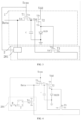
FIG. 1 illustrates a schematic circuit configuration of a drive circuit according to one embodiment of the present application; -
FIG. 2 illustrates a schematic circuit configuration of a compensation circuit in the related art; -
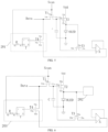
FIG. 3 is one schematic circuit configuration of a compensation circuit according to one embodiment of the present application; -
FIG. 4 is another schematic circuit configuration of the compensation circuit according to one embodiment of the present application; -
FIG. 5 is yet another schematic circuit configuration of the compensation circuit according to one embodiment of the present application; -
FIG. 6 is yet another schematic circuit configuration of the compensation circuit according to one embodiment of the present application; -
FIG. 7 is yet another schematic circuit configuration of the compensation circuit according to one embodiment of the present application; -
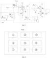
FIG. 8 is a schematic structural diagram of a display panel according to one embodiment of the present application. - In the following descriptions, in order to describe but not intended to limit the present application, concrete details including specific system structure and technique are proposed, so that a comprehensive understanding of the embodiments of the present application is facilitated. However, a person of ordinarily skill in the art should understand that, the present application can also be implemented in some other embodiments from which these concrete details are excluded. In other conditions, detailed explanations of method, circuit, device and system well known to the public are omitted, so that unnecessary details which are disadvantageous to understanding of the description of the present application may be avoided.
- A drive circuit with a model of 2T1C is often used to control an OLED to emit light in an OLED panel. The drive circuit with the model of 2T1C generally includes two thin film transistors (TFTs), a capacitance, and an OLED. For example, as shown in
FIG. 1 , thedrive circuit 1 may include a first TFT T1, a second TFT T2, an OLED and a capacitance C. A control electrode T1a of the first TFT T1 is connected with a scanning line Scan, a first electrode T1b of the first TFT T1 is connected with a data line Data, a second electrode T1c of the first TFT T1 is connected with a control electrode T2a of the second TFT T2, a second electrode T2c of the second TFT T2 is connected with a positive pole of the OLED, a first electrode T2b of the second TFT T2 is connected with a terminal VDD (i.e., a power terminal), and a negative pole of the OLED is grounded. One end of the capacitance C is connected with the second electrode T1c of the first TFT T2, and the other end of the capacitance C is connected with the negative pole of the OLED. - When the scanning line Scan in the
drive circuit 1 receives a high-level signal for the first time, the first TFT T1 is turned on, and the data line Data may charge the capacitance C and exert a voltage on the control electrode T2a of the second TFT T2. After the control electrode T2a of the second TFT T2 receives the voltage of the data line Data, the second TFT T2 is turned on, and the second electrode T2 of the second TFT T2 exerts a voltage on a positive pole of the OLED to enable the OLED to emit light. - When the scanning line Scan receives a low level signal for the first time, the first TFT T1 is turned off, the data line Data cannot exert a voltage on the control electrode T2a of the second TFT T2. At this time, the capacitance C discharges, and the capacitance C supplies a voltage to the control electrode T2a of the second TFT T2 (to keep the second TFT T2 to be switched on), such that the OLED can emit light.
- Due to the fact that the threshold voltage of the TFT is drifted under a long-time bias voltage of gate electrode, however, when the capacitance is discharged, the voltage exerted on the control electrode T2a of the second TFT T2 may be lower than the drifted threshold voltage, the luminance of the OLED is reduced, and the display effect of the OLED is further affected.
- It should be understood that, the circuit configuration of the
drive circuit 1 is not limited in the present application, as long as thedrive circuit 1 includes the first TFT, the second TFT, the OLED, and the capacitance. For example, thedrive circuit 1 is a p-type circuit (i.e., consisting of two TFTs and one capacitance) having a model of 2T1C. - In the related art, a technical solution is existed, that is, a
compensation circuit 2 connected with thedrive circuit 1 is provided in the display panel. As shown inFIG. 2 , thiscompensation circuit 2 includes a first TFT T1-1, a second TFT T1-2, a third TFT T1-3, and a capacitance C2. A control electrode of the first TFT T1-1, a second TFT T1-2, and a third TFT T1-3 are respectively connected with a first scanning line Scan 1(n), a second scanning line Scan 2(n) and a third scanning line Scan 3(n). A first electrode of the first TFT T1-1 is grounded, a second electrode of the first TFT T1-1 is connected with one end of the capacitance C2, a first electrode of the third TFT T1-3 is grounded, a second electrode of the third TFT T1-3 is connected with the other end of the capacitance C2. A first electrode of the second TFT T1-2 is connected with aninternal drive circuit 1, and a second electrode of the second TFT T1-2 is connected with the other end of the capacitance C2. When the scanning line receives the high level signal, the capacitance C1 and the capacitance C2 are charged. When the scanning line receives a low level, the capacitance C2 performs voltage compensation on the capacitance C1 to avoid the threshold voltage from being drifted, which affects the luminescence of the OLED. In this way, a plurality of transistors, scanning lines, and capacitances need to be arranged on the display panel. It can be seen from theFIG. 2 that, the circuit configuration is complex, the circuit arrangement of the display panel is greatly increased, so that an area of one single OLED is increased, and thus the OLED is not attractive in appearance. - A compensation circuit is provided in the present application, the compensation circuit is applied to the
drive circuit 1 and may be arranged on a peripheral chip, the circuit configuration is simple, and the problem that the OLED panel has a low luminance due to the drifting of threshold voltage of the OLED panel is solved, the luminosity factor of the OLED panel is guaranteed. - The
compensation circuit 2 provided in the present application is described with reference to the accompanying drawings. - The
drive circuit 1 shown inFIG. 1 is taken as an example, based onFIG. 1 , as shown inFIG. 3 , thecompensation circuit 2 includes a third TFT T3 and adetection module 201, a control electrode T3a of the third TFT T3 is configured to be connected with the second electrode T2c of the second TFT T2, a first electrode T3b of the third TFT T3 is configured to be connected with the control electrode T2a of the second TFT T2, thedetection module 201 is connected with the second electrode T3c of the third TFT T3, the scan line Scan and the data line Data respectively. Thedetection module 201 is configured to be turned off and turned on respectively when receiving two continuous voltage signals. - When the scanning line Scan in the
drive circuit 1 receives the high-level signal for the first time, the first TFT T1 is switched on, the data line Data charges the capacitance C and exerts a voltage on the control electrode T2a of the second TFT T2 respectively, so that the second TFT T2 is switched on. After the second TFT T2 is switched on, the OLED is enabled to emit light. Moreover, the second electrode T2c of the second TFT T2 exerts a voltage (i.e., Vdd) on the control electrode T3a of the third TFT T3 to enable the third TFT T3 to be switched on. At this time, the first electrode T3b of the third TFT T3 collects a gate voltage Vth of the control electrode T2a of the second TFT T2, and transmits the gate voltage Vth to thedetection module 201 through the second electrode T3c of the third TFT T3. Thedetection module 201 is turned on after receiving the gate voltage Vth and transmits the gate voltage Vth to the data line Data. - When the scanning line Scan in the
drive circuit 1 receives the low level signal for the first time, the first TFT T1 is switched off, and the capacitance C supplies voltage to the control electrode T2a of the second TFT T2 by discharging, so that the second TFT T2 is kept at a switched on state, and the luminance of the OLED is maintained accordingly. - Then, when the scanning line Scan in the
drive circuit 1 receives the high level signal for the second time, the first TFT T1 is switched on, the data line Data charges the data voltage Vdata and the gate voltage Vth into the capacitance C, and exerts a voltage on the control electrode T2a of the second TFT T2, so that the second TFT T2 is switched on. Moreover, the second electrode T2c of the second TFT T2 may exert a voltage on the control electrode T3a of the third TFT to enable the third TFT to be switched on. At this time, the first electrode T3b of the third TFT T3 collects the gate voltage Vth of the control electrode T2a of the second TFT T2, and transmits the gate voltage Vth to thedetection module 201 through the second electrode T3c of the third TFT T3. After receiving the gate electrode Vth, thedetection module 201 is turned off and does not exert voltage on the data line Data. - When the scanning line Scan receives the low level signal for the second time, the first TFT T1 is turned off, the capacitance C is discharged, since the data voltage and the gate voltage Vth for compensating the data voltage Vdata is stored in the capacitance C, such that the second TFT T2 can also enable the OLED to provide excellent luminance at the high level signal under the low level signal, the luminance of the OLED is ensured accordingly. In this way, in the condition of switching between the high level signal and the low level signal, a problem of drifting of the threshold voltage caused due to long-time gate electrode bias voltage is solved, and the luminance of the OLED is ensured under the low-level signal.
- When the scanning line Scan receives the third high-level signal, the
detection module 201 is turned on and outputs the threshold voltage to the data line Data. When receiving two continuous high-level signals, thedetection module 201 is turned off and turned on, respectively, and this process is repeatedly performed. - In one example, in the present application, the detection module may be detected based on a T flip-flop. For example, as shown in
FIG. 4 , the detection module may include a resistor R, a T flip-flop, and a fourth TFT T4. One end of the resistor R (i.e., the end R1 shown inFIG. 4 ) is connected with a clock signal receiving terminal (i.e., the end C1 as shown inFIG. 4 ), the other end (i.e., the end R2 as shown inFIG. 4 ) of the resistor R is connected with the scanning line Scan, a second data signal input (i.e., the terminal T as shown inFIG. 4 ) of the T flip-flop is configured to output a digital signal. When a digital signal "0" is received at the second data signal input, a non-inverting output (i.e., the terminal Q as shown inFIG. 4 ) of the T flip-flop outputs a low level signal. When a digital signal "1" is received at the second data signal input, the terminal Q of the T flip-flop outputs a high level signal. The terminal Q of the T flip-flop is connected with a control electrode T4a of the fourth TFT T4, a second electrode T4b of the fourth TFT T4 is connected with the second electrode T3c of the third TFT T3, and the first electrode T4c of the fourth TFT T4 is connected with the data line Data. - As an example, the T flip-flop may be a falling edge T flip-flop, and a T-terminal of the falling edge T flip-flop in this embodiment of the present application is always at a high level. When a C1 end of the falling edge T flip-flop detects two continuous falling edge signals, the T flip-flop is turned off and turned on respectively, so that the fourth TFT T4 is turned off and turned on correspondingly.
- For example, when the scanning line Scan receives the high-level signal for the first time, the
detection module 201 receives the high-level signal (i.e., the clock control signal) output by the scanning line Scan. When the digital signal "1" is received at the T terminal, the falling edge T flip-flop outputs a high level to enable the fourth TFT T4 to be switched on, so that thedetection module 201 outputs the gate voltage Vth to the data line Data. - When the scanning line Scan in the
drive circuit 1 receives the low level signal for the first time, the first TFT T1 is turned off, and the capacitance C supplies electricity to the control electrode T2a of the second TFT T2 to enable the OLED to emit light. - When the scanning line Scan in the
drive circuit 1 receives the high-level signal for the second time, the terminal C1 of the T flip-flop receives the clock control signal. When the digital signal "1" is received at the terminal T, the terminal Q of the falling edge T flip-flop output a low level signal. After the control electrode T4a of the fourth TFT receives the low level signal, the fourth TFT T4 is turned off, such that the first electrode T4b of the fourth TFT T4 cannot output voltage to the data line Data. Thus, thedetection module 201 can turn off and turn on the fourth TFT T4 respectively when receiving two continuous high-level signals, thereby controlling the compensated gate voltage Vth. - If not, when the scanning line Scan frequently receives high-level signals, the
compensation circuit 2 always exerts a gate voltage Vth on the data line Data, so that the compensated gate voltage Vth is always increasing. Finally, a fault of the OLED panel is caused. - It can be understood that when the threshold voltage changes due to the change of the external environment, the gate voltage Vth detected in the present application is also changed.
- In one example, as shown in
FIG. 5 , thecompensation circuit 2 may further include a voltage follower (i.e., the circuit component A shown inFIG. 5 ), the voltage follower is connected in series between the third TFT T3 and thedetection module 201, a non-inverting input of the voltage follower A (i.e., the terminal "+" of the voltage follower A inFIG. 5 ) is connected with a second electrode T3c of the third TFT T3, an output of the voltage follower A is respectively connected with thedetection module 201 and an inverting input of the voltage follower (i.e., the terminal "-" of the voltage follower A inFIG. 5 ). The voltage follower A is arranged in thecompensation circuit 2, so that a load capacity of thecompensation circuit 2 can be improved, and a problem of loss of gate voltage in a transmission process is alleviated. - In one example, as shown in
FIG. 6 , thecompensation circuit 2 further includes afirst control module 202, thefirst control module 202 is connected with the second electrode T2c of the second TFT T2 and the second control module, respectively, and thefirst control module 202 is configured to control the second control module to output a high level signal and a low level signal alternately according to a signal output by the second electrode T2c of the second TFT T2. The second control module is configured to input the high level signal and the low level signal to the scanning line Scan alternately. In this way, it is unnecessary to additionally arrange pull-up resistors and pull-down resistors for respectively controlling the conversion of the high level signal and low level signal. The conversion of the high level signal and the low level signal can be realized through onesingle control module 202. - For example, the
first control module 202 may include a comparator shown inFIG. 7 (i.e., the circuit component B shown inFIG. 7 ), a D flip-flop, an inverter (i.e., the circuit component E shown inFIG. 5 ), a first metal oxide semiconductor field effect transistor (Metal Oxide Semiconductor Field Effect Transistor, MOSFET) M1 and a second MOSFET M2. A non-inverting input of the comparator B is connected with the second electrode T2c of the second TFT T2, an inverting input (the terminal "-" of the circuit component B shown inFIG. 7 ) is grounded, an output of the comparator B is connected with the control electrode T3a of the third TFT T3. A clock signal receiving terminal (the terminal C1 shown inFIG. 7 ) of the D flip-flop is connected with an output of the comparator B, a data signal input (i.e., the terminal D shown inFIG. 7 ) of the D flip-flop is connected with an output of the inverter E, a non-inverting signal output (i.e., the terminal Q shown inFIG. 7 ) of the D flip-flop is connected with the input of the inverter E, a control electrode M1a of the first MOSFET M1 and a control electrode M2a of the second MOSFET M2, respectively. A second electrode M1c of the first MOSFET M1 and a second electrode M2c of the second MOSFET M2 are connected with the second control module respectively. - In some embodiments, the comparator may be a zero-crossing voltage comparator.
- In some embodiments, the D flip-flop may be a rising edge D flip-flop.
- For example, when the scanning line Scan receives the high level signal for the first time, the first TFT T1 is switched on, and the data line Data charges the capacitance C and exerts a voltage on the control electrode T2a of the second TFT T2 respectively, so that the second TFT T2 is switched on. After the second TFT T2 is switched on, the OLED is enabled to emit light. Moreover, the second electrode T2c of the second TFT T2 exerts a voltage on the non-inverting input (+) of the comparator B, at this time, this voltage is greater than the voltage when the inverting input (-) of the comparator B is grounded, the output of the comparator B outputs a high level, and the comparator B exerts a voltage on the control electrode T3a of the third TFT T3 to enable the third TFT T3 to be switched on. After the signal output from the output of the comparator B is received at the clock signal receiving terminal of the D flip-flop, the data signal input of the D flip-flop is at a high level, such that the non-inverting signal output of the D flip-flop is enabled to output a high level signal. When the inverting signal output of the D flip-flop outputs a high level signal, the high level signal is received at the control terminal M1a of the first MOSFET, the first MOSFET is switched on, the second MOSFET is switched off, so that the first MOSFET M1 output a high level signal to the
second control module 203, and thesecond control module 203 is enabled to output a high level signal to the scanning line Scan. However, since the data signal input of the D flip-flop is connected with the output of the inverter E, and the non-inverting signal output of the D flip-flop is connected with the input of the inverter E, the control electrode M1a of the first MOSFET M1 and the control electrode M2a of the second MOSFET M2, respectively. Thus, after the non-inverting signal output of the D flip-flop outputs a high level signal, the high level enables a digital signal "0" to be input to the data signal input of the D flip-flop through the inverter E, so that the non-inverting signal output of the D flip-flop outputs a low level signal, the high level signal is received at the control electrode M2a of the second MOSFET M2, the second MOSFET M2 is switched on, the first MOSFET M1 is turned off. Thus, the second MOSFET M2 is enabled to output a low level signal to thesecond control module 203 to control the scanning line Scan. Therefore, the D flip-flop can be always kept in a switching mode of receiving a data signal "0" and a data signal "1", thereby achieving the conversion of high level and low level through one signalfirst control module 202. - In one example, in order to avoid variations of circuit characteristics due to the variations of the transistors, the first TFT T1, the second TFT T2, the third TFT T3, and the fourth TFT T4 provided in this embodiment of the present application may be the same transistor.
- Exemplarily, an oxide thin-film transistor (oxide thin-film transistor, Oxide TFT) may be selected. The Oxide TFT is provided with high carrier mobility, low preparation temperature and good electricity homogeneity.
- A control chip is further provided in the second embodiment of the present application. The control chip is connected with the scanning lines of the display panel and is configured to input scanning signals to the scanning lines, and the control chip includes a
compensation circuit 2 provided in the first embodiment. - Where, the control chip may be provided with one
compensation circuit 2, and the first electrode T3b of the third TFT T3 in thecompensation circuit 2 is respectively connected with the control electrodes T2a of the second TFTs T2 of thedrive circuits 1 corresponding to the plurality of OLEDs in the display panel, thereby performing a threshold voltage compensation on the display panel entirely. - In some embodiments, the control chip may be provided with a plurality of
compensation circuits 2, and each of the plurality ofcompensation circuits 2 corresponds to one display area of the display panel. For example, as shown inFIG. 8 , the display panel is divided into 9 display areas, the control chip may be provided with 9compensation circuits 2, and the first electrodes T3b of the third TFTs T3 of the 9compensation circuits 2 are respectively connected with the control electrodes T2a of the second TFTs T2 of thedrive circuits 1 corresponding to the plurality of OLEDs in the 9 display areas, thereby performing the threshold voltage compensation on the corresponding display areas. - In some embodiments,
compensation circuits 2 of the drive circuits corresponding to the plurality of OLEDs in the display panel may also be designed in the control chip, that is, each of the plurality of OLEDs is divided into one display area. - It can be understood that, the more the number of display areas that the display panel are divided into, the more fine the compensation of the gate voltage Vth for each of the display areas is, and the better the display effect of the OLED panel is. The detail of compensation mode may be determined according to the actual requirement.
- Based on the control chip, a display device is further provided in the third embodiment of the present application. The display device includes the control chip provided in the second embodiment.
- It should be understood that, when a term "comprise/include" is used in the description and annexed claims, the term "comprise/include" indicates existence of the described characteristics, integer, steps, operations, elements and/or components, but not exclude existence or adding of one or more other characteristics, integer, steps, operations, elements, components and/or combination thereof.
- It should be further understood that, terms "and/or" used in the description and the annexed claims of the present application are referred to as any combination of one or a plurality of listed item(s) associated with each other and all possible items, and including these combinations.
- Moreover, in the description of the specification and the annexed claims of the present application, terms such as "first" and "second", "third", etc., are only intended to be distinguished in description, but shouldn't be interpreted as indicating or implying a relative importance.
- The descriptions of "referring to one embodiment" and "referring to some embodiments", and the like as described in the specification of the present application means that a specific feature, structure, or characters which are described with reference to this embodiment are included in one embodiment or some embodiments of the present application. Thus, the sentences of "in one embodiment", "in some embodiments", "in some other embodiments", "in other embodiments", and the like in this specification are not necessarily referring to the same embodiment, but instead indicate "one or more embodiments instead of all embodiments", unless otherwise a special emphasis is provided in other manner. The terms "comprising", "including", "having" and their variations mean "including but is not limited to", unless there is a special emphasis in other manner otherwise.
- The aforesaid embodiments are only intended to explain but not to limit the technical solutions of the present application. Although the present application has been described in detail with reference to these embodiments, a person of ordinary skilled in the art should understand that, the technical solutions disclosed in the embodiments may also be amended, some technical features in the technical solutions may also be equivalently replaced. The amendments or the equivalent replacements don't cause the essence of the corresponding technical solutions to be deviated from the spirit and the scope of the technical solutions in the embodiments of the present application, and thus should all be included in the protection scope of the present application.
Claims (15)
- A compensation circuit, being applied to a drive circuit, the drive circuit comprises a first thin film transistor, a second thin film transistor, an organic light-emitting diode and a capacitance;characterized in that, a control electrode of the first thin film transistor is connected with a scanning line, a first electrode of the first thin film transistor is connected with a data line, a second electrode of the first thin film transistor is connected with a control electrode of the second thin film transistor, a second electrode of the second thin film transistor is connected with a positive pole of the organic light-emitting diode, a first electrode of the second thin film transistor is connected with a power terminal, and a negative pole of the organic light-emitting diode is grounded; one end of the capacitance is connected with the second electrode of the first thin film transistor, and the other end of the capacitance is connected with the negative pole of the organic light-emitting diode; the compensation circuit comprises a third thin film transistor and a detection module;a control electrode of the third thin film transistor is configured to be connected with the second electrode of the second thin film transistor, a first electrode of the third thin film transistor is configured to be connected with the control electrode of the second thin film transistor, the detection module is connected with the second electrode of the third thin film transistor, the scanning line and the data line respectively; and the detection module is configured to be turned off and turned on respectively when receiving two continuous voltage signals output from the second electrode of the third thin film transistor.
- The compensation circuit according to claim 1, wherein the detection module comprises a resistor, a T flip-flop, and a fourth thin film transistor;
one end of the resistor is connected with a clock signal receiving terminal of the T flip-flop, the other end of the resistor is connected with the scanning line, a non-inverting signal output of the T flip-flop is connected with a control electrode of the fourth thin film transistor, a second electrode of the fourth thin film transistor is connected with the second electrode of the third thin film transistor, and a first electrode of the fourth thin film transistor is connected with the data line. - The compensation circuit according to claim 2, wherein the first thin film transistor, the second thin film transistor, the third thin film transistor and the fourth thin film transistor are oxide thin film transistors.
- The compensation circuit according to claim 2, wherein the T flip-flop is a falling edge T flip-flop.
- The compensation circuit according to claim 4, wherein a second data signal input of the T flip-flop is high level.
- The compensation circuit according to claim 1, further comprising a voltage follower connected in series between the third thin film transistor and the detection module, wherein a non-inverting input of the voltage follower is connected with the second electrode of the third thin film transistor, and an output of the voltage follower is connected with the detection module and an inverting input of the voltage follower, respectively.
- The compensation circuit according to claim 1, further comprising a first control module, the first control module is respectively connected with the second electrode of the second thin film transistor and a second control module, the first control module is configured to control the second control module to output a high-level signal and a low-level signal alternatively according to a signal output by the second electrode of the second thin-film transistor, the second control module is configured to input the high-level signal and the low-level signal to the scanning line alternatively.
- The compensation circuit according to claim 7, wherein the first control module comprises a comparator, a data flip-flop, an inverter, a first metal oxide semiconductor field effect transistor and a second metal oxide semiconductor field effect transistor;
wherein a non-inverting input of the comparator is connected with the second electrode of the second thin film transistor, an inverting input of the comparator is grounded, an output of the comparator is connected with the control electrode of the third thin film transistor; a clock signal receiving terminal of the D flip-flop is connected with the output of the comparator, a data signal input of the D flip-flop is connected with an output of the inverter, a non-inverting signal output of the D flip-flop is connected with an input of the inverter, a control electrode of the first metal oxide semiconductor field effect transistor, and a control electrode of the second metal oxide semiconductor field effect transistor respectively, a second electrode of the first metal oxide semiconductor field effect transistor and a second electrode of the second metal oxide semiconductor field effect transistor are connected with the second control module, respectively. - The compensation circuit according to claim 8, wherein the comparator is a zero-crossing voltage comparator.
- The compensation circuit according to claim 8, wherein the data flip-flop is a rising edge data flip-flop.
- A control chip, which is connected with a scanning line in a display panel and is configured to input a scanning signal to the scanning line; the control chip comprises a compensation circuit;the compensation circuit is applied to a drive circuit, the drive circuit comprises a first thin film transistor, a second thin film transistor, an organic light-emitting diode and a capacitance; a control electrode of the first thin film transistor is connected with the scanning line, a first electrode of the first thin film transistor is connected with a data line, a second electrode of the first thin film transistor is connected with a control electrode of the second thin film transistor, a second electrode of the second thin film transistor is connected with a positive pole of the organic light-emitting diode, a first electrode of the second thin film transistor is connected with a power terminal, and a negative pole of the organic light-emitting diode is grounded; one end of the capacitance is connected with the second electrode of the first thin film transistor, and the other end of the capacitance is connected with the negative pole of the organic light-emitting diode; the compensation circuit comprises a third thin film transistor and a detection module;a control electrode of the third thin film transistor is configured to be connected with the second electrode of the second thin film transistor, a first electrode of the third thin film transistor is configured to be connected with the control electrode of the second thin film transistor, the detection module is connected with the second electrode of the third thin film transistor, the scanning line and the data line respectively; and the detection module is configured to be turned off and turned on respectively when receiving two continuous voltage signals output from the second electrode of the third thin film transistor.
- The control chip according to claim 11, wherein the control chip comprises one compensation circuit, the first electrode of the third thin film transistor of the compensation circuit is respectively connected to second thin film transistors of the drive circuit corresponding to the various light emitting diodes in the display panel.
- The control chip according to claim 11, wherein the control chip comprises at least one compensation circuit, each compensation circuit corresponds to one display area in the display panel, the first electrode of the third thin film transistor of each compensation circuit is respectively connected to second thin film transistors in the drive circuit corresponding to the various light-emitting diodes in the corresponding display area.
- The control chip according to claim 11, wherein the control chip comprises at least one compensation circuit, the at least one compensation circuit correspond to the light-emitting diodes in the display panel respectively, each of the light-emitting diodes corresponds to one display area.
- A display device, which comprises a control chip;the control chip is connected to a scan line in the display panel, and is configured to input a scan signal to the scan line, the control chip is connected to a scan line in the display panel, and is configured to input a scan signal to the scan line; the control chip comprises a compensation circuit;the compensation circuit is applied to a drive circuit, the drive circuit comprises a first thin film transistor, a second thin film transistor, an organic light-emitting diode (OLED) and a capacitance; wherein a control electrode of the first thin film transistor is connected with a scanning line, a first electrode of the first thin film transistor is connected with a data line, a second electrode of the first thin film transistor is connected with a control electrode of the second thin film transistor, a second electrode of the second thin film transistor is connected with a positive pole of the organic light-emitting diode, a first electrode of the second thin film transistor is connected with a power terminal, and a negative pole of the organic light-emitting diode is grounded; one end of the capacitance is connected with the second electrode of the first thin film transistor, and the other end of the capacitance is connected with the negative pole of the organic light-emitting diode; the compensation circuit comprises a third thin film transistor and a detection module;a control electrode of the third thin film transistor is configured to be connected with the second electrode of the second thin film transistor, a first electrode of the third thin film transistor is configured to be connected with the control electrode of the second thin film transistor, the detection module is connected with the second electrode of the third thin film transistor, the scanning line and the data line respectively; and the detection module is configured to be turned off and turned on respectively when receiving two continuous voltage signals output from the second electrode of the third thin film transistor.
Applications Claiming Priority (2)
| Application Number | Priority Date | Filing Date | Title |
|---|---|---|---|
| CN202210645866.2A CN114743501B (en) | 2022-06-09 | 2022-06-09 | Compensation circuit, control chip and display device |
| PCT/CN2022/140830 WO2023236501A1 (en) | 2022-06-09 | 2022-12-21 | Compensation circuit, control chip and display apparatus |
Publications (2)
| Publication Number | Publication Date |
|---|---|
| EP4539028A1 true EP4539028A1 (en) | 2025-04-16 |
| EP4539028A4 EP4539028A4 (en) | 2026-03-04 |
Family
ID=82288059
Family Applications (1)
| Application Number | Title | Priority Date | Filing Date |
|---|---|---|---|
| EP22945629.8A Pending EP4539028A4 (en) | 2022-06-09 | 2022-12-21 | Compensation circuit, control chip and display apparatus |
Country Status (6)
| Country | Link |
|---|---|
| US (1) | US11961467B2 (en) |
| EP (1) | EP4539028A4 (en) |
| JP (1) | JP7683168B2 (en) |
| KR (1) | KR102768800B1 (en) |
| CN (1) | CN114743501B (en) |
| WO (1) | WO2023236501A1 (en) |
Families Citing this family (8)
| Publication number | Priority date | Publication date | Assignee | Title |
|---|---|---|---|---|
| CN114743501B (en) * | 2022-06-09 | 2022-08-23 | 惠科股份有限公司 | Compensation circuit, control chip and display device |
| CN115019729B (en) * | 2022-08-04 | 2022-11-25 | 惠科股份有限公司 | Pixel driving circuit, display panel and control method thereof |
| CN115312001B (en) | 2022-10-12 | 2022-12-09 | 惠科股份有限公司 | Pixel driving circuit, driving method thereof, and display device |
| CN116741101A (en) * | 2023-06-30 | 2023-09-12 | 惠科股份有限公司 | Pixel driving circuit, display panel and display device |
| CN117153098B (en) * | 2023-08-30 | 2026-05-01 | 惠科股份有限公司 | Pixel circuit and display panel |
| CN117095641A (en) * | 2023-09-04 | 2023-11-21 | 维沃移动通信有限公司 | Display module, detection method and electronic equipment |
| CN119007684B (en) * | 2024-09-30 | 2025-08-15 | 惠科股份有限公司 | Transistor compensation circuit, transistor compensation method and display panel |
| CN120220597B (en) * | 2025-05-28 | 2025-12-26 | 惠科股份有限公司 | Display driving circuit and display panel |
Family Cites Families (25)
| Publication number | Priority date | Publication date | Assignee | Title |
|---|---|---|---|---|
| JPH0775079B2 (en) * | 1986-10-16 | 1995-08-09 | パイオニア株式会社 | Truck jump control device |
| AU1908788A (en) * | 1987-07-17 | 1989-01-19 | Nutronics Corporation | Method and apparatus for managing alternator loads on engines |
| JP4573544B2 (en) * | 2004-03-09 | 2010-11-04 | 三菱電機株式会社 | Display device |
| KR101171188B1 (en) * | 2005-11-22 | 2012-08-06 | 삼성전자주식회사 | Display device and driving method thereof |
| CN102044212B (en) * | 2009-10-21 | 2013-03-20 | 京东方科技集团股份有限公司 | Voltage driving pixel circuit, driving method thereof and organic lighting emitting display (OLED) |
| CN103198793B (en) * | 2013-03-29 | 2015-04-29 | 京东方科技集团股份有限公司 | Pixel circuit, drive method and display device thereof |
| KR101603300B1 (en) * | 2013-11-25 | 2016-03-14 | 엘지디스플레이 주식회사 | Organic light emitting display device and display panel |
| JP6832634B2 (en) | 2015-05-29 | 2021-02-24 | 株式会社半導体エネルギー研究所 | Semiconductor device |
| US10360827B2 (en) * | 2015-10-09 | 2019-07-23 | Apple Inc. | Systems and methods for indirect threshold voltage sensing in an electronic display |
| CN106504707B (en) | 2016-10-14 | 2018-06-01 | 深圳市华星光电技术有限公司 | OLED pixel mixed compensation circuit and mixed compensation method |
| CN106328061B (en) | 2016-10-14 | 2019-03-12 | 深圳市华星光电技术有限公司 | OLED pixel mixed compensation circuit and mixed compensation method |
| CN106409225B (en) * | 2016-12-09 | 2019-03-01 | 上海天马有机发光显示技术有限公司 | Organic light-emitting pixel compensation circuit, organic light-emitting display panel and driving method |
| CN106782330B (en) * | 2016-12-20 | 2019-03-12 | 上海天马有机发光显示技术有限公司 | Organic light-emitting pixel driving circuit, driving method and organic light-emitting display panel |
| KR102636683B1 (en) | 2016-12-30 | 2024-02-14 | 엘지디스플레이 주식회사 | Orgainc emitting diode display device |
| CN106548753B (en) * | 2017-01-20 | 2018-06-01 | 深圳市华星光电技术有限公司 | AMOLED pixel drivers system and AMOLED image element driving methods |
| CN106935192B (en) * | 2017-05-12 | 2019-04-02 | 京东方科技集团股份有限公司 | Pixel circuit and driving method thereof, and display device |
| US11462144B2 (en) | 2018-09-28 | 2022-10-04 | Sharp Kabushiki Kaisha | Display device and driving method therefor |
| CN109119026B (en) * | 2018-09-29 | 2020-06-23 | 京东方科技集团股份有限公司 | A pixel circuit data signal compensation method, device and display panel |
| CN110827763B (en) | 2019-11-07 | 2021-07-06 | 深圳市华星光电半导体显示技术有限公司 | Pixel circuit, driving method thereof and display device |
| EP4068360B1 (en) * | 2019-11-29 | 2026-04-15 | BOE Technology Group Co., Ltd. | Display substrate, manufacturing method therefor, and display device |
| CN111063302A (en) | 2019-12-17 | 2020-04-24 | 深圳市华星光电半导体显示技术有限公司 | Pixel hybrid compensation circuit and pixel hybrid compensation method |
| CN111402789B (en) * | 2020-04-08 | 2021-03-16 | 深圳市华星光电半导体显示技术有限公司 | Pixel driving circuit and display panel |
| KR102801691B1 (en) * | 2020-06-12 | 2025-04-30 | 삼성디스플레이 주식회사 | Pixel circuit and organic light emitting display |
| CN114550656B (en) * | 2022-03-02 | 2022-12-02 | 绵阳惠科光电科技有限公司 | Drive circuit, drive device, and display device |
| CN114743501B (en) | 2022-06-09 | 2022-08-23 | 惠科股份有限公司 | Compensation circuit, control chip and display device |
-
2022
- 2022-06-09 CN CN202210645866.2A patent/CN114743501B/en active Active
- 2022-12-21 WO PCT/CN2022/140830 patent/WO2023236501A1/en not_active Ceased
- 2022-12-21 US US18/069,429 patent/US11961467B2/en active Active
- 2022-12-21 KR KR1020237024614A patent/KR102768800B1/en active Active
- 2022-12-21 EP EP22945629.8A patent/EP4539028A4/en active Pending
- 2022-12-21 JP JP2023556898A patent/JP7683168B2/en active Active
Also Published As
| Publication number | Publication date |
|---|---|
| WO2023236501A1 (en) | 2023-12-14 |
| US11961467B2 (en) | 2024-04-16 |
| KR102768800B1 (en) | 2025-02-18 |
| EP4539028A4 (en) | 2026-03-04 |
| US20230402004A1 (en) | 2023-12-14 |
| JP7683168B2 (en) | 2025-05-27 |
| CN114743501B (en) | 2022-08-23 |
| KR20230170640A (en) | 2023-12-19 |
| CN114743501A (en) | 2022-07-12 |
| JP2024526510A (en) | 2024-07-19 |
Similar Documents
| Publication | Publication Date | Title |
|---|---|---|
| US11961467B2 (en) | Compensation circuit, control chip and display device | |
| US10991307B2 (en) | Pixel circuit and driving method thereof, display device | |
| US9589505B2 (en) | OLED pixel circuit, driving method of the same, and display device | |
| US11735115B2 (en) | Pixel driving circuit having two data signals to compensate for threshold voltage and driving method | |
| US20210217341A1 (en) | Gate drive circuit and drive method thereof, display device and control method thereof | |
| US10878734B1 (en) | Driving circuit, tiled electronic device, and test method | |
| US20200380910A1 (en) | Pixel circuit, drive method thereof and display panel | |
| US11257423B2 (en) | Pixel driving circuit and driving method thereof, and display panel | |
| US20220301510A1 (en) | Shift register and control method therefor, gate driving circuit, and display panel | |
| US10649509B2 (en) | Display device capable of detecting whether a power cable is abnormally connected | |
| CN113270067B (en) | Pixel circuit and display panel | |
| CN111243498B (en) | Pixel circuit and driving method thereof, and display device | |
| US11244623B2 (en) | Pixel circuit and driving method thereof | |
| US7982704B2 (en) | Data driving circuit and electroluminescent display using the same | |
| CN107731143B (en) | Test circuit and test method of AMOLED display and AMOLED display | |
| US20150317936A1 (en) | Shift register unit, gate driving apparatus and display device | |
| US20200168140A1 (en) | Display panel | |
| US11322076B2 (en) | Pixel driving chip and driving method therefor, and display apparatus | |
| CN114299847A (en) | Light emitting device driving circuit and display panel | |
| KR102727501B1 (en) | Display device and driving method thereof | |
| US12494167B2 (en) | Pixel drive circuit and drive method thereof, and display apparatus | |
| US20210358389A1 (en) | Pixel driving circuit, pixel driving method and display device | |
| CN113763872B (en) | Pixel circuit, driving method thereof and display device | |
| US9805655B2 (en) | Pixel circuit and driving method thereof, display device | |
| CN110070830B (en) | Pixel driving circuit and display panel |
Legal Events
| Date | Code | Title | Description |
|---|---|---|---|
| STAA | Information on the status of an ep patent application or granted ep patent |
Free format text: STATUS: THE INTERNATIONAL PUBLICATION HAS BEEN MADE |
|
| PUAI | Public reference made under article 153(3) epc to a published international application that has entered the european phase |
Free format text: ORIGINAL CODE: 0009012 |
|
| STAA | Information on the status of an ep patent application or granted ep patent |
Free format text: STATUS: REQUEST FOR EXAMINATION WAS MADE |
|
| 17P | Request for examination filed |
Effective date: 20240326 |
|
| AK | Designated contracting states |
Kind code of ref document: A1 Designated state(s): AL AT BE BG CH CY CZ DE DK EE ES FI FR GB GR HR HU IE IS IT LI LT LU LV MC ME MK MT NL NO PL PT RO RS SE SI SK SM TR |
|
| DAV | Request for validation of the european patent (deleted) | ||
| DAX | Request for extension of the european patent (deleted) | ||
| A4 | Supplementary search report drawn up and despatched |
Effective date: 20260129 |
|
| RIC1 | Information provided on ipc code assigned before grant |
Ipc: G09G 3/3208 20160101AFI20260123BHEP Ipc: G09G 3/32 20160101ALI20260123BHEP Ipc: G09G 3/3225 20160101ALI20260123BHEP |