EP4538760A1 - Optical communication device using conformal coating layer as optical waveguide - Google Patents
Optical communication device using conformal coating layer as optical waveguide Download PDFInfo
- Publication number
- EP4538760A1 EP4538760A1 EP23865680.5A EP23865680A EP4538760A1 EP 4538760 A1 EP4538760 A1 EP 4538760A1 EP 23865680 A EP23865680 A EP 23865680A EP 4538760 A1 EP4538760 A1 EP 4538760A1
- Authority
- EP
- European Patent Office
- Prior art keywords
- optical
- coating layer
- optical element
- conformal coating
- pcb
- Prior art date
- Legal status (The legal status is an assumption and is not a legal conclusion. Google has not performed a legal analysis and makes no representation as to the accuracy of the status listed.)
- Pending
Links
Images





Classifications
-
- G—PHYSICS
- G02—OPTICS
- G02B—OPTICAL ELEMENTS, SYSTEMS OR APPARATUS
- G02B6/00—Light guides; Structural details of arrangements comprising light guides and other optical elements, e.g. couplings
- G02B6/10—Light guides; Structural details of arrangements comprising light guides and other optical elements, e.g. couplings of the optical waveguide type
- G02B6/12—Light guides; Structural details of arrangements comprising light guides and other optical elements, e.g. couplings of the optical waveguide type of the integrated circuit kind
- G02B6/122—Basic optical elements, e.g. light-guiding paths
-
- G—PHYSICS
- G02—OPTICS
- G02B—OPTICAL ELEMENTS, SYSTEMS OR APPARATUS
- G02B6/00—Light guides; Structural details of arrangements comprising light guides and other optical elements, e.g. couplings
- G02B6/24—Coupling light guides
- G02B6/42—Coupling light guides with opto-electronic elements
- G02B6/4201—Packages, e.g. shape, construction, internal or external details
- G02B6/4274—Electrical aspects
- G02B6/428—Electrical aspects containing printed circuit boards [PCB]
-
- G—PHYSICS
- G02—OPTICS
- G02B—OPTICAL ELEMENTS, SYSTEMS OR APPARATUS
- G02B6/00—Light guides; Structural details of arrangements comprising light guides and other optical elements, e.g. couplings
- G02B6/10—Light guides; Structural details of arrangements comprising light guides and other optical elements, e.g. couplings of the optical waveguide type
- G02B6/12—Light guides; Structural details of arrangements comprising light guides and other optical elements, e.g. couplings of the optical waveguide type of the integrated circuit kind
- G02B6/122—Basic optical elements, e.g. light-guiding paths
- G02B6/1221—Basic optical elements, e.g. light-guiding paths made from organic materials
-
- H—ELECTRICITY
- H05—ELECTRIC TECHNIQUES NOT OTHERWISE PROVIDED FOR
- H05K—PRINTED CIRCUITS; CASINGS OR CONSTRUCTIONAL DETAILS OF ELECTRIC APPARATUS; MANUFACTURE OF ASSEMBLAGES OF ELECTRICAL COMPONENTS
- H05K1/00—Printed circuits
- H05K1/02—Details
-
- H—ELECTRICITY
- H05—ELECTRIC TECHNIQUES NOT OTHERWISE PROVIDED FOR
- H05K—PRINTED CIRCUITS; CASINGS OR CONSTRUCTIONAL DETAILS OF ELECTRIC APPARATUS; MANUFACTURE OF ASSEMBLAGES OF ELECTRICAL COMPONENTS
- H05K1/00—Printed circuits
- H05K1/02—Details
- H05K1/0274—Optical details, e.g. printed circuits comprising integral optical means
-
- H—ELECTRICITY
- H05—ELECTRIC TECHNIQUES NOT OTHERWISE PROVIDED FOR
- H05K—PRINTED CIRCUITS; CASINGS OR CONSTRUCTIONAL DETAILS OF ELECTRIC APPARATUS; MANUFACTURE OF ASSEMBLAGES OF ELECTRICAL COMPONENTS
- H05K3/00—Apparatus or processes for manufacturing printed circuits
- H05K3/22—Secondary treatment of printed circuits
- H05K3/28—Applying non-metallic protective coatings
-
- H—ELECTRICITY
- H05—ELECTRIC TECHNIQUES NOT OTHERWISE PROVIDED FOR
- H05K—PRINTED CIRCUITS; CASINGS OR CONSTRUCTIONAL DETAILS OF ELECTRIC APPARATUS; MANUFACTURE OF ASSEMBLAGES OF ELECTRICAL COMPONENTS
- H05K3/00—Apparatus or processes for manufacturing printed circuits
- H05K3/22—Secondary treatment of printed circuits
- H05K3/28—Applying non-metallic protective coatings
- H05K3/284—Applying non-metallic protective coatings for encapsulating mounted components
-
- H—ELECTRICITY
- H05—ELECTRIC TECHNIQUES NOT OTHERWISE PROVIDED FOR
- H05K—PRINTED CIRCUITS; CASINGS OR CONSTRUCTIONAL DETAILS OF ELECTRIC APPARATUS; MANUFACTURE OF ASSEMBLAGES OF ELECTRICAL COMPONENTS
- H05K3/00—Apparatus or processes for manufacturing printed circuits
- H05K3/22—Secondary treatment of printed circuits
- H05K3/28—Applying non-metallic protective coatings
- H05K3/285—Permanent coating compositions
-
- G—PHYSICS
- G02—OPTICS
- G02B—OPTICAL ELEMENTS, SYSTEMS OR APPARATUS
- G02B6/00—Light guides; Structural details of arrangements comprising light guides and other optical elements, e.g. couplings
- G02B6/10—Light guides; Structural details of arrangements comprising light guides and other optical elements, e.g. couplings of the optical waveguide type
- G02B6/12—Light guides; Structural details of arrangements comprising light guides and other optical elements, e.g. couplings of the optical waveguide type of the integrated circuit kind
- G02B6/122—Basic optical elements, e.g. light-guiding paths
- G02B6/125—Bends, branchings or intersections
-
- G—PHYSICS
- G02—OPTICS
- G02B—OPTICAL ELEMENTS, SYSTEMS OR APPARATUS
- G02B6/00—Light guides; Structural details of arrangements comprising light guides and other optical elements, e.g. couplings
- G02B6/24—Coupling light guides
- G02B6/42—Coupling light guides with opto-electronic elements
- G02B6/4201—Packages, e.g. shape, construction, internal or external details
- G02B6/4246—Bidirectionally operating package structures
-
- G—PHYSICS
- G02—OPTICS
- G02B—OPTICAL ELEMENTS, SYSTEMS OR APPARATUS
- G02B6/00—Light guides; Structural details of arrangements comprising light guides and other optical elements, e.g. couplings
- G02B6/24—Coupling light guides
- G02B6/42—Coupling light guides with opto-electronic elements
- G02B6/4201—Packages, e.g. shape, construction, internal or external details
- G02B6/4251—Sealed packages
- G02B6/4253—Sealed packages by embedding housing components in an adhesive or a polymer material
-
- G—PHYSICS
- G02—OPTICS
- G02B—OPTICAL ELEMENTS, SYSTEMS OR APPARATUS
- G02B6/00—Light guides; Structural details of arrangements comprising light guides and other optical elements, e.g. couplings
- G02B6/24—Coupling light guides
- G02B6/42—Coupling light guides with opto-electronic elements
- G02B6/43—Arrangements comprising a plurality of opto-electronic elements and associated optical interconnections
Definitions
- optical communication technology which is a means for quick signal transmission between components of an electronic device
- signal transmission may be performed at higher speeds, and disadvantages of existing signal transmission methods, such as high resistance, high heat generation, and parasitic capacitance, may be alleviated.
- Embodiments disclosed herein aim to provide an optical communication device that uses, as an optical waveguide for optical communication, a conformal coating layer of a printed circuit board (PCB) where optical elements are arranged.
- PCB printed circuit board
- the first conformal coating layer may be configured to contact an optical signal input/output unit of the first optical element and an optical signal input/output unit of the second optical element.
- the first conformal coating layer may be configured to avoid contacting optical elements other than the first optical element and the second optical element among a plurality of optical elements arranged on the PCB.
- the second surface may include a third surface where the first conformal coating layer contacts the first optical element, a fourth surface where the first conformal coating layer contacts the second optical element, and a fifth surface except for the third surface and the fourth surface.
- the second conformal coating layer may be configured to contact the entire fifth surface.
- a refractive index of the first conformal coating layer may be greater than a refractive index of the PCB and a refractive index of the second conformal coating layer.
- optical communication between optical elements where a line of sight (LoS) is not secured may be enabled.
- LiS line of sight
- FIG. 1 is a block diagram showing a configuration of an optical communication device according to an embodiment.
- the PCB 110 may have mounted thereon components of the optical communication device 100 (e.g., the first optical element 120 and/or the second optical element 130).
- the PCB 110 may be a metal-core PCB (MPCB) based on metal having good thermal conductivity.
- the PCB 110 may be based on an insulating substrate material.
- the PCB 110 may be implemented as various types and structures.
- FIG. 3 is a plan view and a cross-sectional view showing an arrangement state of a PCB, a first optical element, a second optical element, and a conformal coating layer of an optical communication device, according to an embodiment.
- the conformal coating layer 300 may transmit the optical signal by using total reflection characteristics of light.
- the conformal coating layer 300 may include a material that allows an optical signal traveling therein to be totally reflected from a surface thereof.
- the conformal coating layer 300 may include a material having a greater refractive index than a refractive index of a material contacting the surface thereof.
- the first optical element 120 may perform an optical signal input/output unit 121 or 131.
- the optical signal input/output unit 121 or 131 may include an optical signal output unit TX for outputting an optical signal and an optical signal input unit RX for receiving an optical signal.
- the first optical element 120 (or the second optical element 130) may output an optical signal through the optical signal output unit TX and receive an optical signal through the optical signal input unit RX.
- the conformal coating layer 400 may transmit the optical signal by using total reflection characteristics of light.
- the conformal coating layer 400 may include a material that allows an optical signal traveling therein to be totally reflected from a surface thereof.
- the conformal coating layer 400 may include a material having a greater refractive index than a refractive index of a material contacting the surface thereof.
- FIG. 5 is a plan view showing an arrangement state of a PCB, a first optical element, a second optical element, a third optical element, and a conformal coating layer of an optical communication device, according to an embodiment.
- the conformal coating layer 510 may be coated onto at least a part of the surface of the PCB 110.
- the conformal coating layer 300 may be formed of a polymer material.
- the conformal coating layer 510 may not contact the third optical element 520 to prevent an optical signal traveling therein from being input to the third optical element 520.
- the conformal coating layer 510 may be used as an optical waveguide in optical communication between the first optical element 120 and the second optical element 130. According to an embodiment, the conformal coating layer 510 may transmit the optical signal output from the first optical element 120 (or the second optical element 130) to the second optical element 130 (or the first optical element 120). To this end, the conformal coating layer 510 may contact the optical signal input/output unit 121 or 131 of the first optical element 120 and the second optical element 130.
- the conformal coating layer 510 may transmit the optical signal by using total reflection characteristics of light.
- the conformal coating layer 510 may include a material that allows an optical signal traveling therein to be totally reflected from a surface thereof.
- the conformal coating layer 510 may include a material having a greater refractive index than a refractive index of a material contacting the surface thereof.
- optical communication may be possible through the conformal coating layer 510 used as an optical waveguide.
- FIG. 6 is a plan view showing an arrangement state of a PCB, a first optical element, a second optical element, and a conformal coating layer of an optical communication device, according to an embodiment.
- FIGS. 7A and 7B are a plan view and a cross-sectional view showing an arrangement state of a PCB, a first optical element, a second optical element, a first conformal coating layer, and a second conformal coating layer of an optical communication device, according to an embodiment.
- the second surface of the first conformal coating layer 710 may include a third surface contacting the first optical element 120, a fourth surface contacting the second optical element 130, and a fifth surface except for the third surface and the fourth surface.
- the second conformal coating layer 720 may be coated onto the entire fifth surface of the second surface of the first conformal coating layer 710.
- the first conformal coating layer 710 may include a material having a greater refractive index than a refractive index of the PCB 110 contacting the surface thereof and a refractive index of the second conformal coating layer 720.
- FIGS. 8A and 8B are a plan view and a cross-sectional view showing an arrangement state of a PCB, a first optical element, a second optical element, a third optical element, a first conformal coating layer, and a second conformal coating layer of an optical communication device, according to an embodiment.
- FIG. 8B is a cross-sectional view cut from a plan view of FIG. 8A along a line C1-C2.
- the first optical element 120 may perform an optical signal input/output unit 121 or 131.
- the optical signal input/output unit 121 or 131 may include an optical signal output unit TX for outputting an optical signal and an optical signal input unit RX for receiving an optical signal.
- the first optical element 120 (or the second optical element 130) may output an optical signal through the optical signal output unit TX and receive an optical signal through the optical signal input unit RX.
- the first conformal coating layer 810 may be used as an optical waveguide in optical communication between the first optical element 120 and the second optical element 130. According to an embodiment, the first conformal coating layer 810 may transmit the optical signal output from the first optical element 120 (or the second optical element 130) to the second optical element 130 (or the first optical element 120). To this end, the first conformal coating layer 810 may contact the optical signal input/output units 121 and 131 of the first optical element 120 and the second optical element 130.
- a corner portion of the first conformal coating layer 810 may have a designated curvature such that an optical signal incident from the first optical element 120 (or the second optical element 130) is totally reflected and thus travels to the second optical element 130 (or the first optical element 120).
- the second surface of the first conformal coating layer 810 may include a third surface contacting the first optical element 120, a fourth surface contacting the second optical element 130, and a fifth surface except for the third surface and the fourth surface.
- the second conformal coating layer 820 may be coated onto the entire fifth surface of the second surface of the first conformal coating layer 810.
- the first conformal coating layer 810 may include a material having a greater refractive index than a refractive index of the PCB 110 contacting the surface thereof and a refractive index of the second conformal coating layer 820.
- optical communication may be possible through the first conformal coating layer 810 used as an optical waveguide.
Landscapes
- Engineering & Computer Science (AREA)
- Microelectronics & Electronic Packaging (AREA)
- Physics & Mathematics (AREA)
- Manufacturing & Machinery (AREA)
- General Physics & Mathematics (AREA)
- Optics & Photonics (AREA)
- Optical Couplings Of Light Guides (AREA)
- Optical Integrated Circuits (AREA)
- Non-Metallic Protective Coatings For Printed Circuits (AREA)
Abstract
Description
- This application claims priority to and the benefit of
Korean Patent Application No. 10-2022-0117485 filed in the Korean Intellectual Property Office on September 16, 2022 - Embodiments disclosed herein relate to an optical communication device using a conformal coating layer as an optical waveguide.
- With the recent advancement of autonomous driving and advanced driver assistance systems (ADAS), bandwidth increase and integrity of data are required and data integrity and electromagnetic compatibility (EMC) issues are encountered. Consequently, optical communication technology has been introduced, which is capable of replacing standards such as a local interconnect network (LIN), a controller area network (CAN), a controller area network flexible data-rate (CAN FD), and FlexRay, etc., conventionally used for vehicle communication.
- When the optical communication technology, which is a means for quick signal transmission between components of an electronic device, is applied to the electronic device, signal transmission may be performed at higher speeds, and disadvantages of existing signal transmission methods, such as high resistance, high heat generation, and parasitic capacitance, may be alleviated.
- Conventionally, optical cables have been used as optical waveguides for optical communication. However, for the optical cables, due to their high cost and flexibility, it is not free to secure a line of sight (LoS) of a component for transmitting and receiving an optical communication signal, resulting in limitations in use for short-range communication inside vehicles.
- Embodiments disclosed herein aim to provide an optical communication device that uses, as an optical waveguide for optical communication, a conformal coating layer of a printed circuit board (PCB) where optical elements are arranged.
- Technical problems of the embodiments disclosed herein are not limited to the above-described technical problems, and other unmentioned technical problems would be clearly understood by one of ordinary skill in the art from the following description.
- An optical communication device according to an embodiment disclosed herein includes a first optical element, a second optical element capable of performing optical communication with the first optical element, a printed circuit board (PCB) where the first optical element and the second optical element are arranged, and a first conformal coating layer of a polymer material, coated onto at least a part of a surface of the PCB, in which the optical communication is performed using the first conformal coating layer as an optical waveguide.
- In the optical communication device according to an embodiment disclosed herein, the first conformal coating layer may be configured to contact an optical signal input/output unit of the first optical element and an optical signal input/output unit of the second optical element.
- In the optical communication device according to an embodiment disclosed herein, the first conformal coating layer may be configured to avoid contacting optical elements other than the first optical element and the second optical element among a plurality of optical elements arranged on the PCB.
- In the optical communication device according to an embodiment disclosed herein, the first conformal coating layer may include a material that allows an optical signal traveling inside the first conformal coating layer to be totally reflected from a surface of the first conformal coating layer.
- In the optical communication device according to an embodiment disclosed herein, a refractive index of the first conformal coating layer may be greater than a refractive index of the PCB.
- The optical communication device according to an embodiment disclosed herein may further include a second conformal coating layer of a polymer material, coated onto at least a part of a second surface that is different from a first surface contacting the PCB among surfaces of the first conformal coating layer.
- In the optical communication device according to an embodiment disclosed herein, the second surface may include a third surface where the first conformal coating layer contacts the first optical element, a fourth surface where the first conformal coating layer contacts the second optical element, and a fifth surface except for the third surface and the fourth surface.
- In the optical communication device according to an embodiment disclosed herein, the second conformal coating layer may be configured to contact the entire fifth surface.
- In the optical communication device according to an embodiment disclosed herein, a refractive index of the first conformal coating layer may be greater than a refractive index of the PCB and a refractive index of the second conformal coating layer.
- According to embodiments disclosed herein, a conformal coating layer of a PCB may perform optical communication between optical elements by using a conformal coating layer of a PCB as an optical waveguide, without adding a separate component (e.g., an optical cable, a connector, etc.).
- According to embodiments disclosed herein, optical communication between optical elements where a line of sight (LoS) is not secured may be enabled.
- Moreover, various effects recognized directly or indirectly from the disclosure may be provided.
-
-
FIG. 1 is a block diagram showing a configuration of an optical communication device according to an embodiment. -
FIG. 2 is a view for describing a method where an optical waveguide transmits an optical signal by using total reflection characteristics of light. -
FIG. 3 is a plan view showing an arrangement state of a PCB, a first optical element, a second optical element, and a conformal coating layer of an optical communication device, according to an embodiment. -
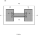
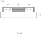
FIGS. 4A and4B are a plan view and a cross-sectional view showing an arrangement state of a PCB, a first optical element, a second optical element, and a conformal coating layer of an optical communication device, according to an embodiment. -
FIG. 5 is a plan view showing an arrangement state of a PCB, a first optical element, a second optical element, a third optical element, and a conformal coating layer of an optical communication device, according to an embodiment. -
FIG. 6 is a plan view showing an arrangement state of a PCB, a first optical element, a second optical element, and a conformal coating layer of an optical communication device, according to an embodiment. -
FIGS. 7A and7B are a plan view and a cross-sectional view showing an arrangement state of a PCB, a first optical element, a second optical element, a first conformal coating layer, and a second conformal coating layer of an optical communication device, according to an embodiment. -
FIGS. 8A and8B are a plan view and a cross-sectional view showing an arrangement state of a PCB, a first optical element, a second optical element, a third optical element, a first conformal coating layer, and a second conformal coating layer of an optical communication device, according to an embodiment. - Hereinafter, various embodiments of the present disclosure will be disclosed with reference to the accompanying drawings. However, the description is not intended to limit the present disclosure to particular embodiments, and it should be construed as including various modifications, equivalents, and/or alternatives according to the embodiments of the present disclosure.
- It should be appreciated that various embodiments of the present document and the terms used therein are not intended to limit the technological features set forth herein to particular embodiments and include various changes, equivalents, or replacements for a corresponding embodiment. With regard to the description of the drawings, similar reference numerals may be used to refer to similar or related elements. It is to be understood that a singular form of a noun corresponding to an item may include one or more of the things, unless the relevant context clearly indicates otherwise.
- As used herein, each of such phrases as "A or B," "at least one of A and B," "at least one of A or B," "A, B, or C," "at least one of A, B, and C," and "at least one of A, B, or C," may include any one of, or all possible combinations of the items enumerated together in a corresponding one of the phrases. Such terms as "1st", "2nd," "first", "second", "A", "B", "(a)", or "(b)" may be used to simply distinguish a corresponding component from another, and does not limit the components in other aspect (e.g., importance or order), unless mentioned otherwise.
- Herein, it is to be understood that when an element (e.g., a first element) is referred to, with or without the term "operatively" or "communicatively", as "connected with", "coupled with", or "linked with", or "coupled to" or "connected to" to another element (e.g., a second element), it means that the element may be connected with the other element directly (e.g., wiredly), wirelessly, or via a third element.
- According to an embodiment of the disclosure, a method according to various embodiments of the disclosure disclosed herein may be included and provided in a computer program product. The computer program product may be traded as a product between a seller and a buyer. The computer program product may be distributed in the form of a machine-readable storage medium (e.g., compact disc read only memory (CD-ROM)), or be distributed (e.g., downloaded or uploaded) online via an application store, or between two user devices directly. If distributed online, at least part of the computer program product may be temporarily generated or at least temporarily stored in the machine-readable storage medium, such as memory of the manufacturer's server, a server of the application store, or a relay server.
- According to various embodiments, each component (e.g., an element or a program) of the above-described components may include a single entity or multiple entities, and some of the multiple entities may be separately disposed in different components. According to various embodiments, one or more of the above-described components may be omitted, or one or more other components may be added. Alternatively or additionally, a plurality of components (e.g., elements or programs) may be integrated into a single component. In such a case, according to various embodiments, the integrated component may still perform one or more functions of each of the plurality of components in the same or similar manner as they are performed by a corresponding one of the plurality of components before the integration. According to various embodiments, operations performed by the element, the program, or another component may be carried out sequentially, in parallel, repeatedly, or heuristically, or one or more of the operations may be executed in a different order or omitted, or one or more other operations may be added.
-
FIG. 1 is a block diagram showing a configuration of an optical communication device according to an embodiment. - Referring to
FIG. 1 , anoptical communication device 100 may include a printed circuit board (PCB) 110, a firstoptical element 120, a secondoptical element 130, and anoptical waveguide 140. - The PCB 110 may have mounted thereon components of the optical communication device 100 (e.g., the first
optical element 120 and/or the second optical element 130). According to an embodiment, the PCB 110 may be a metal-core PCB (MPCB) based on metal having good thermal conductivity. According to another embodiment, the PCB 110 may be based on an insulating substrate material. However, without being limited to these examples, the PCB 110 may be implemented as various types and structures. - The first optical element 120 (or the second optical element 130) may perform optical communication with the second optical element 130 (or the first optical element 120). According to an embodiment, the first
optical element 120 and the secondoptical element 130 may transmit and receive optical signals to and from each other by using anoptical waveguide 140. The first optical element 120 (or the second optical element 130) may transmit an optical signal to the second optical element 130 (or the first optical element 120) by using theoptical waveguide 140 or receive the optical signal from the second optical element 130 (or the first optical element 120). - The
optical waveguide 140 may transmit the optical signal output from the first optical element 120 (or the second optical element 130) to the second optical element 130 (or the first optical element 120). According to an embodiment, theoptical waveguide 140 may transmit the optical signal by using total reflection characteristics of light. To this end, theoptical waveguide 140 may include a material that allows an optical signal traveling inside theoptical waveguide 140 to be totally reflected from a surface of theoptical waveguide 140. For example, theoptical waveguide 140 may include a material having a greater refractive index than a refractive index of a material contacting the surface thereof. According to an embodiment, theoptical waveguide 140 may be implemented using a conformal coating layer of a polymer material coated onto at least a part of a surface of thePCB 110. -
FIG. 2 is a view for describing a method where an optical waveguide transmits an optical signal by using total reflection characteristics of light.FIG. 2 will be described using components ofFIG. 1 . - Referring to
FIG. 2 , anoptical waveguide module 200 may include acore layer 210, alower cladding layer 220, and anupper cladding layer 230. According to an embodiment, thecore layer 210 may contact thelower cladding layer 220 and theupper cladding layer 230. - According to an embodiment, the
optical waveguide module 200 may transmit an optical signal by using characteristics where an optical signal incident to thecore layer 210 operating as an optical waveguide (e.g., theoptical waveguide 140 ofFIG. 1 ) is totally reflected from a surface of thecore layer 210. To this end, thecore layer 210 may include a material having a refractive index n1 greater than a refractive index n2 of thelower cladding layer 220 and a refractive index n3 of theupper cladding layer 230. - According to an embodiment, the
core layer 210 may be implemented using a conformal coating layer of a polymer material coated onto at least a part of the surface of thePCB 110. In this case, thelower cladding layer 220 is implemented with thePCB 110, but theupper cladding layer 230 may be implemented with air or a conformal coating layer of a material different from that of thecore layer 210. - For example, when the surface of the
PCB 110 is conformally coated with a single material, thecore layer 210 operating as the optical waveguide may be implemented with a conformal coating layer and theupper cladding layer 230 may be implemented with air. In this case, the conformal coating layer may include a material having the refractive index n1 greater than the refractive index n2 of thePCB 110 and the refractive index n3 of air. - In another example, when the surface of the
PCB 110 is conformally coated with dual materials, thecore layer 210 operating as the optical waveguide may be implemented with a first conformal coating layer and theupper cladding layer 230 may be implemented with a second conformal coating layer including a material that is different from that of the first conformal coating layer. In this case, the first conformal coating layer may include a material having the refractive index n1 greater than the refractive index n2 of thePCB 110 and the refractive index n3 of the second conformal coating layer. -
FIG. 3 is a plan view and a cross-sectional view showing an arrangement state of a PCB, a first optical element, a second optical element, and a conformal coating layer of an optical communication device, according to an embodiment. - Referring to
FIG. 3 , theoptical communication device 100 may include thePCB 110, the firstoptical element 120, the secondoptical element 130, and aconformal coating layer 300. - The first optical element 120 (or the second optical element 130) may perform an optical signal input/
output unit output unit - The
conformal coating layer 300 may be coated onto at least a part of the surface of thePCB 110. Herein, theconformal coating layer 300 may be formed of a polymer material. - According to an embodiment, the
conformal coating layer 300 may be used as an optical waveguide in optical communication between the firstoptical element 120 and the secondoptical element 130. According to an embodiment, theconformal coating layer 300 may transmit the optical signal output from the first optical element 120 (or the second optical element 130) to the second optical element 130 (or the first optical element 120). To this end, theconformal coating layer 300 may contact the optical signal input/output unit optical element 120 and the secondoptical element 130. For example, theconformal coating layer 300 may include a first coating layer that contacts the optical signal output unit TX of the firstoptical element 120 and the optical signal input unit RX of the secondoptical element 130 and a second coating layer that contacts the optical signal input unit RX of the firstoptical element 120 and the optical signal output unit TX of the secondoptical element 130 and does not contact the first coating layer. In another example, theconformal coating layer 300 may include one coating layer that contacts the optical signal input/output unit 121 of the firstoptical element 120 and the optical signal input/output unit 131 of the secondoptical element 130. - According to an embodiment, the
conformal coating layer 300 may transmit the optical signal by using total reflection characteristics of light. To this end, theconformal coating layer 300 may include a material that allows an optical signal traveling therein to be totally reflected from a surface thereof. For example, theconformal coating layer 300 may include a material having a greater refractive index than a refractive index of a material contacting the surface thereof. -
FIGS. 4A and4B are a plan view and a cross-sectional view showing an arrangement state of a PCB, a first optical element, a second optical element, and a conformal coating layer of an optical communication device, according to an embodiment. - In particular,
FIG. 4B is a cross-sectional view cut from a plan view ofFIG. 4A along a line A1-A2. - Referring to
FIGS. 4A and4B , theoptical communication device 100 may include thePCB 110, the firstoptical element 120, the secondoptical element 130, and aconformal coating layer 400. - The first optical element 120 (or the second optical element 130) may perform an optical signal input/
output unit output unit - The
conformal coating layer 400 may be coated onto at least a part of the surface of thePCB 110, and may be coated onto the entire surface that does not contact thePCB 110 among surfaces of the firstoptical element 120 and the secondoptical element 130. Herein, theconformal coating layer 400 may be formed of a polymer material. - According to an embodiment, the
conformal coating layer 400 may be used as an optical waveguide in optical communication between the firstoptical element 120 and the secondoptical element 130. According to an embodiment, theconformal coating layer 400 may transmit the optical signal output from the first optical element 120 (or the second optical element 130) to the second optical element 130 (or the first optical element 120). To this end, theconformal coating layer 400 may contact the optical signal input/output unit optical element 120 and the secondoptical element 130. - According to an embodiment, the
conformal coating layer 400 may transmit the optical signal by using total reflection characteristics of light. To this end, theconformal coating layer 400 may include a material that allows an optical signal traveling therein to be totally reflected from a surface thereof. For example, theconformal coating layer 400 may include a material having a greater refractive index than a refractive index of a material contacting the surface thereof. -
FIG. 5 is a plan view showing an arrangement state of a PCB, a first optical element, a second optical element, a third optical element, and a conformal coating layer of an optical communication device, according to an embodiment. - Referring to
FIG. 5 , theoptical communication device 100 may include thePCB 110, the firstoptical element 120, the secondoptical element 130, a thirdoptical element 520, and aconformal coating layer 510. - The first optical element 120 (or the second optical element 130) may perform an optical signal input/
output unit output unit - The
conformal coating layer 510 may be coated onto at least a part of the surface of thePCB 110. Herein, theconformal coating layer 300 may be formed of a polymer material. According to an embodiment, theconformal coating layer 510 may not contact the thirdoptical element 520 to prevent an optical signal traveling therein from being input to the thirdoptical element 520. - According to an embodiment, the
conformal coating layer 510 may be used as an optical waveguide in optical communication between the firstoptical element 120 and the secondoptical element 130. According to an embodiment, theconformal coating layer 510 may transmit the optical signal output from the first optical element 120 (or the second optical element 130) to the second optical element 130 (or the first optical element 120). To this end, theconformal coating layer 510 may contact the optical signal input/output unit optical element 120 and the secondoptical element 130. - According to an embodiment, the
conformal coating layer 510 may transmit the optical signal by using total reflection characteristics of light. To this end, theconformal coating layer 510 may include a material that allows an optical signal traveling therein to be totally reflected from a surface thereof. For example, theconformal coating layer 510 may include a material having a greater refractive index than a refractive index of a material contacting the surface thereof. - According to an embodiment, a corner portion of the
conformal coating layer 510 may have a designated curvature such that an optical signal incident from the first optical element 120 (or the second optical element 130) is totally reflected and thus travels to the second optical element 130 (or the first optical element 120). - Referring to
FIG. 5 , even when an LoS is not secured between optical signal input/output units of the firstoptical element 120 and the secondoptical element 130 that transmit and receive optical signals therebetween through optical communication, optical communication may be possible through theconformal coating layer 510 used as an optical waveguide. -
FIG. 6 is a plan view showing an arrangement state of a PCB, a first optical element, a second optical element, and a conformal coating layer of an optical communication device, according to an embodiment. - Referring to
FIG. 6 , theoptical communication device 100 may include thePCB 110, the firstoptical element 120, the secondoptical element 130, and aconformal coating layer 600. - The first optical element 120 (or the second optical element 130) may perform an optical signal input/
output unit output unit - The
conformal coating layer 600 may be coated onto at least a part of the surface of thePCB 110. Herein, theconformal coating layer 600 may be formed of a polymer material. - According to an embodiment, the
conformal coating layer 600 may be used as an optical waveguide in optical communication between the firstoptical element 120 and the secondoptical element 130. According to an embodiment, theconformal coating layer 600 may transmit the optical signal output from the first optical element 120 (or the second optical element 130) to the second optical element 130 (or the first optical element 120). To this end, theconformal coating layer 600 may contact the optical signal input/output unit optical element 120 and the secondoptical element 130. - According to an embodiment, the
conformal coating layer 600 may transmit the optical signal by using total reflection characteristics of light. To this end, theconformal coating layer 600 may include a material that allows an optical signal traveling therein to be totally reflected from a surface thereof. For example, theconformal coating layer 600 may include a material having a greater refractive index than a refractive index of a material contacting the surface thereof. - According to an embodiment, a corner portion of the
conformal coating layer 600 may have a designated curvature such that an optical signal incident from the first optical element 120 (or the second optical element 130) is totally reflected and thus travels to the second optical element 130 (or the first optical element 120). - Referring to
FIG. 6 , even when an LoS is not secured between optical signal input/output units of the firstoptical element 120 and the secondoptical element 130 that transmit and receive optical signals therebetween through optical communication, optical communication may be possible through theconformal coating layer 600 used as an optical waveguide. -
FIGS. 7A and7B are a plan view and a cross-sectional view showing an arrangement state of a PCB, a first optical element, a second optical element, a first conformal coating layer, and a second conformal coating layer of an optical communication device, according to an embodiment. - In particular,
FIG. 7B is a cross-sectional view cut from a plan view ofFIG. 7A along a line B1-B2. - Referring to
FIGS. 7A and7B , theoptical communication device 100 may include thePCB 110, the firstoptical element 120, the secondoptical element 130, a firstconformal coating layer 710, and a secondconformal coating layer 720. - The first optical element 120 (or the second optical element 130) may perform an optical signal input/
output unit output unit - The first
conformal coating layer 710 may be coated onto at least a part of the surface of thePCB 110. Herein, the firstconformal coating layer 710 may be formed of a polymer material. - According to an embodiment, the first
conformal coating layer 710 may be used as an optical waveguide in optical communication between the firstoptical element 120 and the secondoptical element 130. According to an embodiment, the firstconformal coating layer 710 may transmit the optical signal output from the first optical element 120 (or the second optical element 130) to the second optical element 130 (or the first optical element 120). To this end, the firstconformal coating layer 710 may contact the optical signal input/output unit optical element 120 and the secondoptical element 130. - According to an embodiment, the first
conformal coating layer 710 may transmit the optical signal by using total reflection characteristics of light. To this end, the firstconformal coating layer 710 may include a material that allows an optical signal traveling therein to be totally reflected from a surface thereof. For example, the firstconformal coating layer 710 may include a material having a greater refractive index than a refractive index of a material contacting the surface thereof. - According to an embodiment, the second
conformal coating layer 720 may be coated onto at least a part of a second surface that is different from a first surface contacting thePCB 110 among the surfaces of the firstconformal coating layer 710. Herein, the secondconformal coating layer 720 may be formed of a polymer material. - Referring to
FIGS. 7A and7B , the second surface of the firstconformal coating layer 710 may include a third surface contacting the firstoptical element 120, a fourth surface contacting the secondoptical element 130, and a fifth surface except for the third surface and the fourth surface. According to an embodiment, the secondconformal coating layer 720 may be coated onto the entire fifth surface of the second surface of the firstconformal coating layer 710. In this case, the firstconformal coating layer 710 may include a material having a greater refractive index than a refractive index of thePCB 110 contacting the surface thereof and a refractive index of the secondconformal coating layer 720. -
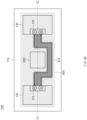
FIGS. 8A and8B are a plan view and a cross-sectional view showing an arrangement state of a PCB, a first optical element, a second optical element, a third optical element, a first conformal coating layer, and a second conformal coating layer of an optical communication device, according to an embodiment. - In particular,
FIG. 8B is a cross-sectional view cut from a plan view ofFIG. 8A along a line C1-C2. - Referring to
FIGS. 8A and8B , theoptical communication device 100 may include thePCB 110, the firstoptical element 120, the secondoptical element 130, a thirdoptical element 830, a firstconformal coating layer 810, and a secondconformal coating layer 820. - The first optical element 120 (or the second optical element 130) may perform an optical signal input/
output unit output unit - The first
conformal coating layer 810 may be coated onto at least a part of the surface of thePCB 110. Herein, the firstconformal coating layer 810 may be formed of a polymer material. According to an embodiment, the firstconformal coating layer 810 may not contact the thirdoptical element 830 to prevent an optical signal traveling therein from being input to the thirdoptical element 830. - According to an embodiment, the first
conformal coating layer 810 may be used as an optical waveguide in optical communication between the firstoptical element 120 and the secondoptical element 130. According to an embodiment, the firstconformal coating layer 810 may transmit the optical signal output from the first optical element 120 (or the second optical element 130) to the second optical element 130 (or the first optical element 120). To this end, the firstconformal coating layer 810 may contact the optical signal input/output units optical element 120 and the secondoptical element 130. - According to an embodiment, the first
conformal coating layer 810 may transmit the optical signal by using total reflection characteristics of light. To this end, the firstconformal coating layer 810 may include a material that allows an optical signal traveling therein to be totally reflected from a surface thereof. For example, the firstconformal coating layer 810 may include a material having a greater refractive index than a refractive index of a material contacting the surface thereof. - According to an embodiment, a corner portion of the first
conformal coating layer 810 may have a designated curvature such that an optical signal incident from the first optical element 120 (or the second optical element 130) is totally reflected and thus travels to the second optical element 130 (or the first optical element 120). - According to an embodiment, the second
conformal coating layer 820 may be coated onto at least a part of a second surface that is different from a first surface contacting thePCB 110 among the surfaces of the firstconformal coating layer 810. Herein, the secondconformal coating layer 820 may be formed of a polymer material. - Referring to
FIGS. 8A and8B , the second surface of the firstconformal coating layer 810 may include a third surface contacting the firstoptical element 120, a fourth surface contacting the secondoptical element 130, and a fifth surface except for the third surface and the fourth surface. According to an embodiment, the secondconformal coating layer 820 may be coated onto the entire fifth surface of the second surface of the firstconformal coating layer 810. In this case, the firstconformal coating layer 810 may include a material having a greater refractive index than a refractive index of thePCB 110 contacting the surface thereof and a refractive index of the secondconformal coating layer 820. - Referring to
FIGS. 8A and8B , even when an LoS is not secured between optical signal input/output units of the firstoptical element 120 and the secondoptical element 130 that transmit and receive optical signals therebetween through optical communication, optical communication may be possible through the firstconformal coating layer 810 used as an optical waveguide. - Terms such as "include", "constitute" or "have" described above may mean that the corresponding component may be inherent unless otherwise stated, and thus should be construed as further including other components rather than excluding other components. All terms including technical or scientific terms have the same meanings as those generally understood by those of ordinary skill in the art to which the embodiments disclosed herein pertain, unless defined otherwise. The terms used generally like terms defined in dictionaries should be interpreted as having meanings that are the same as the contextual meanings of the relevant technology and should not be interpreted as having ideal or excessively formal meanings unless they are clearly defined in the present document.
Claims (9)
- An optical communication device comprising:a first optical element;a second optical element configured to perform optical communication with the first optical element;a printed circuit board (PCB) where the first optical element and the second optical element are arranged; anda first conformal coating layer of a polymer material, coated onto at least a part of a surface of the PCB,wherein the optical communication is performed using the first conformal coating layer as an optical waveguide.
- The optical communication device of claim 1, wherein the first conformal coating layer is configured to contact an optical signal input/output unit of the first optical element and an optical signal input/output unit of the second optical element.
- The optical communication device of claim 1, wherein the first conformal coating layer is configured to avoid contacting optical elements other than the first optical element and the second optical element among a plurality of optical elements arranged on the PCB.
- The optical communication device of claim 1, wherein the first conformal coating layer comprises a material that allows an optical signal traveling inside the first conformal coating layer to totally reflect from a surface of the first conformal coating layer.
- The optical communication device of claim 4, wherein a refractive index of the first conformal coating layer is greater than a refractive index of the PCB.
- The optical communication device of claim 1, further comprising a second conformal coating layer of a polymer material, coated onto at least a part of a second surface that is different from a first surface contacting the PCB among surfaces of the first conformal coating layer.
- The optical communication device of claim 6, wherein the second surface comprises a third surface where the first conformal coating layer contacts the first optical element, a fourth surface where the first conformal coating layer contacts the second optical element, and a fifth surface that is not the third surface and the fourth surface.
- The optical communication device of claim 7, wherein the second conformal coating layer is configured to contact an entirety of the fifth surface.
- The optical communication device of claim 6, wherein a refractive index of the first conformal coating layer is greater than a refractive index of the PCB and a refractive index of the second conformal coating layer.
Applications Claiming Priority (2)
| Application Number | Priority Date | Filing Date | Title |
|---|---|---|---|
| KR1020220117485A KR20240038513A (en) | 2022-09-16 | 2022-09-16 | Optical communiation apparatus using conformal coating layer as optical waveguide |
| PCT/KR2023/009173 WO2024058376A1 (en) | 2022-09-16 | 2023-06-29 | Optical communication device using conformal coating layer as optical waveguide |
Publications (2)
| Publication Number | Publication Date |
|---|---|
| EP4538760A1 true EP4538760A1 (en) | 2025-04-16 |
| EP4538760A4 EP4538760A4 (en) | 2025-10-15 |
Family
ID=90275445
Family Applications (1)
| Application Number | Title | Priority Date | Filing Date |
|---|---|---|---|
| EP23865680.5A Pending EP4538760A4 (en) | 2022-09-16 | 2023-06-29 | OPTICAL COMMUNICATION DEVICE USING CONFORMAL COATING LAYER AS OPTICAL WAVEGUIDE |
Country Status (5)
| Country | Link |
|---|---|
| EP (1) | EP4538760A4 (en) |
| JP (1) | JP2025523660A (en) |
| KR (1) | KR20240038513A (en) |
| CN (1) | CN119452281A (en) |
| WO (1) | WO2024058376A1 (en) |
Family Cites Families (11)
| Publication number | Priority date | Publication date | Assignee | Title |
|---|---|---|---|---|
| JPS5749288A (en) * | 1980-09-09 | 1982-03-23 | Toshiba Corp | Photo hybrid integrated circuit |
| CA2095652C (en) * | 1992-05-07 | 1997-03-25 | Susan L. Oldham | Molded metallized plastic microwave components and processes for manufacture |
| US8529993B2 (en) * | 2006-05-01 | 2013-09-10 | Zetta Research andDevelopment LLC—RPO Series | Low volatility polymers for two-stage deposition processes |
| KR20130064647A (en) * | 2011-12-08 | 2013-06-18 | 엘지이노텍 주식회사 | Optical printed circuit board and fabricating method of the same |
| JP5877749B2 (en) * | 2012-03-29 | 2016-03-08 | 日東電工株式会社 | Manufacturing method of opto-electric hybrid board |
| US9696490B2 (en) * | 2014-04-09 | 2017-07-04 | Texas Instuments Incorporated | Matching impedance of a dielectric waveguide to a launching mechanism |
| KR102082905B1 (en) * | 2016-08-31 | 2020-02-28 | 주식회사 엘지화학 | Conformal coating method for Printed Circuit Board assembly |
| KR20210010120A (en) * | 2019-07-19 | 2021-01-27 | 주식회사 지엠에스아이엔씨 | Generating method for board image for confomal coating |
| EP4040515A4 (en) * | 2019-09-30 | 2023-10-25 | Kyocera Corporation | Optical waveguide package and light emitting device |
| JP7660859B2 (en) * | 2020-04-30 | 2025-04-14 | ウニフェルジテイト・ヘント | Colloidal quantum dot emitters and detectors |
| KR102569564B1 (en) | 2021-02-17 | 2023-08-22 | 한국화학연구원 | Nano-silica-epoxy resin, nano-silica-containing organic/inorganic composite resin, and a method for producing the same. |
-
2022
- 2022-09-16 KR KR1020220117485A patent/KR20240038513A/en active Pending
-
2023
- 2023-06-29 EP EP23865680.5A patent/EP4538760A4/en active Pending
- 2023-06-29 JP JP2025500936A patent/JP2025523660A/en active Pending
- 2023-06-29 WO PCT/KR2023/009173 patent/WO2024058376A1/en not_active Ceased
- 2023-06-29 CN CN202380050323.9A patent/CN119452281A/en active Pending
Also Published As
| Publication number | Publication date |
|---|---|
| KR20240038513A (en) | 2024-03-25 |
| EP4538760A4 (en) | 2025-10-15 |
| JP2025523660A (en) | 2025-07-23 |
| WO2024058376A1 (en) | 2024-03-21 |
| CN119452281A (en) | 2025-02-14 |
Similar Documents
| Publication | Publication Date | Title |
|---|---|---|
| US7477809B1 (en) | Photonic guiding device | |
| CN103814314B (en) | Optical module | |
| CN108376847B (en) | Hybrid cable-to-board connector | |
| EP2972533B1 (en) | Circuit board assemblies employing optical interfaces optically connected to surface-accessible, planar-shaped, inter-board optical fiber traces, and related methods | |
| EP2666044B1 (en) | An optical communication module, and a method for mounting an optical communications system | |
| US20050135742A1 (en) | Coupler assembly for an optical backplane system | |
| WO2009017768A1 (en) | System and methods for routing optical signals | |
| US6259840B1 (en) | Printed circuit board having fluid-linked optical pathways for coupling surface mounted optoelectric semiconductor devices | |
| US20100142881A1 (en) | Optical link circuit and method of making same | |
| KR20060111639A (en) | Low delay optical memory bus | |
| CN102213805A (en) | Opto-electronic transceiver module with castellated electrical turn | |
| CN110311733A (en) | Single-Wavelength Bidirectional Transceiver with Integrated Fiber Coupler | |
| JPWO2018042984A1 (en) | Optical connection structure | |
| US8861917B2 (en) | Opto-electric circuit board including metal-slotted optical waveguide and opto-electric simultaneous communication system | |
| WO2007080932A1 (en) | Optical cable module and apparatus employing it | |
| Immonen et al. | Development of electro-optical PCBs with embedded waveguides for data center and high performance computing applications | |
| CN119452281A (en) | Optical communication devices using conformal coatings as optical waveguides | |
| JP2012503784A (en) | Polarization-maintaining large core hollow waveguide | |
| JP7436416B2 (en) | Multimode waveguide systems and connectors for optical integrated circuits | |
| US6396968B2 (en) | Optical signal transmission device | |
| EP4741897A1 (en) | Active electro-optical cable assembly for high-density data transmission systems | |
| Shiraishi et al. | 24-ch microlens-integrated no-polish connector for optical interconnection with polymer waveguides | |
| Griese et al. | Optical interconnection technology on the printed circuit board level | |
| WO2010149445A1 (en) | Optical module and installation method | |
| US20060165415A1 (en) | Communication cable |
Legal Events
| Date | Code | Title | Description |
|---|---|---|---|
| STAA | Information on the status of an ep patent application or granted ep patent |
Free format text: STATUS: THE INTERNATIONAL PUBLICATION HAS BEEN MADE |
|
| PUAI | Public reference made under article 153(3) epc to a published international application that has entered the european phase |
Free format text: ORIGINAL CODE: 0009012 |
|
| STAA | Information on the status of an ep patent application or granted ep patent |
Free format text: STATUS: REQUEST FOR EXAMINATION WAS MADE |
|
| 17P | Request for examination filed |
Effective date: 20250110 |
|
| AK | Designated contracting states |
Kind code of ref document: A1 Designated state(s): AL AT BE BG CH CY CZ DE DK EE ES FI FR GB GR HR HU IE IS IT LI LT LU LV MC ME MK MT NL NO PL PT RO RS SE SI SK SM TR |
|
| A4 | Supplementary search report drawn up and despatched |
Effective date: 20250917 |
|
| RIC1 | Information provided on ipc code assigned before grant |
Ipc: G02B 6/122 20060101AFI20250911BHEP Ipc: G02B 6/42 20060101ALI20250911BHEP Ipc: H05K 1/02 20060101ALI20250911BHEP Ipc: H05K 3/28 20060101ALI20250911BHEP Ipc: G02B 6/125 20060101ALN20250911BHEP Ipc: G02B 6/43 20060101ALN20250911BHEP |
|
| DAV | Request for validation of the european patent (deleted) | ||
| DAX | Request for extension of the european patent (deleted) | ||
| STAA | Information on the status of an ep patent application or granted ep patent |
Free format text: STATUS: EXAMINATION IS IN PROGRESS |
|
| 17Q | First examination report despatched |
Effective date: 20260401 |