EP4538232A1 - Perovskite compound and photoelectric conversion element - Google Patents
Perovskite compound and photoelectric conversion element Download PDFInfo
- Publication number
- EP4538232A1 EP4538232A1 EP23819838.6A EP23819838A EP4538232A1 EP 4538232 A1 EP4538232 A1 EP 4538232A1 EP 23819838 A EP23819838 A EP 23819838A EP 4538232 A1 EP4538232 A1 EP 4538232A1
- Authority
- EP
- European Patent Office
- Prior art keywords
- perovskite
- layer
- photoelectric conversion
- type compound
- conversion element
- Prior art date
- Legal status (The legal status is an assumption and is not a legal conclusion. Google has not performed a legal analysis and makes no representation as to the accuracy of the status listed.)
- Pending
Links
Images


Classifications
-
- C—CHEMISTRY; METALLURGY
- C01—INORGANIC CHEMISTRY
- C01G—COMPOUNDS CONTAINING METALS NOT COVERED BY SUBCLASSES C01D OR C01F
- C01G21/00—Compounds of lead
- C01G21/006—Compounds containing lead, with or without oxygen or hydrogen, and containing two or more other elements
-
- C—CHEMISTRY; METALLURGY
- C03—GLASS; MINERAL OR SLAG WOOL
- C03C—CHEMICAL COMPOSITION OF GLASSES, GLAZES OR VITREOUS ENAMELS; SURFACE TREATMENT OF GLASS; SURFACE TREATMENT OF FIBRES OR FILAMENTS MADE FROM GLASS, MINERALS OR SLAGS; JOINING GLASS TO GLASS OR OTHER MATERIALS
- C03C17/00—Surface treatment of glass, not in the form of fibres or filaments, by coating
- C03C17/22—Surface treatment of glass, not in the form of fibres or filaments, by coating with other inorganic material
-
- C—CHEMISTRY; METALLURGY
- C01—INORGANIC CHEMISTRY
- C01P—INDEXING SCHEME RELATING TO STRUCTURAL AND PHYSICAL ASPECTS OF SOLID INORGANIC COMPOUNDS
- C01P2002/00—Crystal-structural characteristics
- C01P2002/30—Three-dimensional structures
- C01P2002/34—Three-dimensional structures perovskite-type (ABO3)
-
- Y—GENERAL TAGGING OF NEW TECHNOLOGICAL DEVELOPMENTS; GENERAL TAGGING OF CROSS-SECTIONAL TECHNOLOGIES SPANNING OVER SEVERAL SECTIONS OF THE IPC; TECHNICAL SUBJECTS COVERED BY FORMER USPC CROSS-REFERENCE ART COLLECTIONS [XRACs] AND DIGESTS
- Y02—TECHNOLOGIES OR APPLICATIONS FOR MITIGATION OR ADAPTATION AGAINST CLIMATE CHANGE
- Y02E—REDUCTION OF GREENHOUSE GAS [GHG] EMISSIONS, RELATED TO ENERGY GENERATION, TRANSMISSION OR DISTRIBUTION
- Y02E10/00—Energy generation through renewable energy sources
- Y02E10/50—Photovoltaic [PV] energy
- Y02E10/549—Organic PV cells
Definitions
- the present invention relates to a perovskite-type compound and a photoelectric conversion element.
- the perovskite solar cell has a so-called p-i-n type laminated structure in which a hole transport layer made of a p-type semiconductor, a perovskite layer, and an electron transport layer made of an n-type semiconductor are arranged in this order from the light-receiving side.
- the perovskite layer contains a compound having a perovskite type crystal structure.
- the compound having the perovskite-type crystal structure is represented by the general formula A-B-X 3 .
- Non Patent Literature 1 Non Patent Literature 2, and Non Patent Literature 3
- translucency means that 10% or more of light having any wavelength of 200 nm to 2000 nm is transmitted.
- the first conductive layer 12, the electron transport layer 13, the light absorbing layer 14, the hole transport layer 15, the second conductive layer 16, and the third conductive layer 17 are described later.
- Fig. 2 is a thickness direction cross-sectional view illustrating another example of the photoelectric conversion element according to the embodiment.
- the photoelectric conversion element shown in Fig. 2 may be a perovskite-type solar cell including a light absorbing layer that comprises a compound having a perovskite structure.
- the photoelectric conversion element illustrated in Fig. 2 is a so-called multi-junction photoelectric conversion element.
- a multi-junction photoelectric conversion element includes a plurality of photoelectric conversion cells laminated on each other. That is, the multi-junction photoelectric conversion element may include a plurality of light absorbing layers.
- the photoelectric conversion element 10A has a laminated structure in which a top cell TC and a bottom cell BC are laminated on each other.
- light enters the photoelectric conversion element 10A from the top cell TC side (upper side in the drawing).
- the top cell TC side upper side in the drawing.
- the incident light light on a short wavelength side is photoelectrically converted by the top cell TC.
- the bottom cell BC light on the long wavelength side that has passed through the top cell TC is photoelectrically converted by the bottom cell BC.
- the bottom cell BC may include a substrate 20, a first electrode layer 21, a photoelectric conversion layer (light absorbing layer) 22, a buffer layer 23, and a second electrode layer 24.
- the first electrode layer 21 may be provided on the substrate 20.
- the photoelectric conversion layer 22 may be provided on the first electrode layer 21.
- the buffer layer 23 may be provided on the photoelectric conversion layer 22.
- the second electrode layer 24 may be provided on the buffer layer 23.
- the bottom cell BC for example, a configuration of a known photoelectric conversion element (for example, a solar cell) such as a compound photoelectric conversion element such as a CZTS photoelectric conversion element, a CIGS photoelectric conversion element, a CdTe photoelectric conversion element, or a GaAs photoelectric conversion element, or a silicon photoelectric conversion element or an organic photoelectric conversion element can be applied. Therefore, any explanation regarding the configuration of the bottom cell BC is omitted.
- the buffer layer 23 of the bottom cell BC may be omitted.
- the photoelectric conversion element 10A illustrated in Fig. 2 has a so-called four-terminal tandem structure including four terminals including two positive electrodes and two negative electrodes.
- the photoelectric conversion element 10A may have an intermediate layer 19 between the top cell TC and the bottom cell BC.
- the intermediate layer 19 may be a transparent insulating layer.
- the photoelectric conversion element may have a two-terminal tandem structure.
- the photoelectric conversion element may not include at least the second conductive layer 16, the third conductive layer 17, and the second electrode layer 24 illustrated in Fig. 2 .
- the first conductive layer 12, the electron transport layer 13, the light absorbing layer 14, the hole transport layer 15, the second conductive layer 16, and the third conductive layer 17 described above are described in detail.
- the first conductive layer 12 may be a layer that acts as an anode of the photoelectric conversion element.
- Examples of the material of the first conductive layer 12 include: conductive transparent materials such as copper iodide (CuI), indium tin oxide (ITO), tin oxide (SnO 2 ), fluorine doped tin oxide (FTO), aluminum doped zinc oxide (AZO), indium zinc oxide (IZO), and gallium doped zinc oxide (GZO); metal sodium; a sodium-potassium alloy; metal lithium; metal magnesium; metal aluminum; a magnesium-silver mixture; a magnesium-indium mixture; an aluminum-lithium alloy; an aluminum-aluminum oxide (Al/Al 2 O 3 ) mixture; and an aluminum-lithium fluoride (Al/LiF) mixture.
- the above materials may be used singly or as a mixture of two or more kinds thereof.
- the electron transport layer 13 has a function of transporting electrons generated by photoexcitation of the light absorbing layer 14 to the first conductive layer 12. Therefore, the electron transport layer 13 is preferably formed of a material having characteristics in which electrons generated in the light absorbing layer 14 can easily move to the electron transport layer 13 and in which electrons of the electron transport layer 13 can easily move to the first conductive layer 12.
- the dense layer 13a has a denser structure than the porous layer 13b. In other words, the number of voids in the dense layer 13a is smaller than the number of voids in the porous layer 13b.
- the dense layer 13a is a layer in which a solution or the like used for forming the light absorbing layer 14 hardly infiltrates.
- the dense layer 13a has a function of preventing contact between the first conductive layer 12 and the second conductive layer 16 and has a function of preventing contact between the first conductive layer 12 and the hole transport layer 15, the contacts causing a decrease in photovoltaic power. Therefore, reduction in photovoltaic power can be suppressed by the dense layer 13a.
- the porous layer 13b can be formed by the following method. First, for example, a coating liquid containing titanium oxide particles is prepared, and the coating liquid is coated onto the dense layer 13a by a film forming method such as a spin coating method, a screen printing method, a spray pyrolysis method, or an aerosol deposition method. Thereafter, the porous layer 13b containing titanium oxide is formed by firing. Although not particularly limited, when the porous layer 13b is formed of titanium oxide, anatase type titanium oxide particles are preferably used.
- the hole transport layer 15 is positioned between the light absorbing layer 14 and the second conductive layer 16.
- the hole transport layer 15 has a function of capturing holes generated in the light absorbing layer 14 and has a function of moving the holes to the second conductive layer 16 as a cathode.
- the hole transport layer 15 may contain a matrix component composed of, for example, 2,2',7,7'-tetrakis-(N,N-di-p-methoxyphenylamine)9,9'-spirobifluorene (Spiro-OMeTAD) or poly[bis(4-phenyl) (2,4,6-trimethylphenyl)amine] (PTAA), or may contain an organic low molecular weight thin film that preferentially captures holes such as [2-(9Hcarbazol-9-yl)ethyl] phosphonic acid (2PACz).
- a passivate layer (not illustrated) made of a metal oxide or an organic thin film may be provided between the light absorbing layer 14 and the hole transport layer 15.
- the thickness of the hole transport layer 15 is preferably in a range of 1 nm to 500 nm, and more preferably in a range of 1 nm or more and 130 nm or less.
- the hole transport layer 15 may be an amorphous layer.
- the hole transport layer 15 may contain an organic binder resin or a plasticizer, and the like.
- the hole transport layer 15 can be formed by, for example, the following manufacturing method. First, a compound of said matrix component is dissolved in an organic solvent to prepare a coating liquid, and the coating liquid is coated onto the light absorbing layer 14 (or the passivate layer). Thereafter, the organic solvent is removed to form the hole transport layer 15.
- the organic solvent used for forming the hole transport layer 15 is preferably a solvent that does not disturb the crystal structure of the organic-inorganic hybrid compound because the organic solvent is coated onto the light absorbing layer 14. Examples of the solvent include chlorobenzene, toluene and isopropanol, and so on.
- the coating method of the coating liquid is not particularly limited, and examples thereof include a spin coating method, a screen printing method, and a dip coating method.
- the second conductive layer 16 is a transparent conductive layer having translucency, and acts as an cathode of the photoelectric conversion element.
- the second conductive layer 16 is formed on the hole transport layer 15 and is in contact with the hole transport layer 15.
- any conductive transparent material can be used.
- the material of the second conductive layer 16 is preferably a metal oxide containing, for example, any of indium, zinc and tin.
- Examples of the material of the second conductive layer 16 include conductive transparent materials and conductive transparent polymers such as copper iodide (CuI), indium tin oxide (ITO), tin oxide (SnO 2 ), fluorine-doped tin oxide (FTO), aluminum-doped zinc oxide (AZO), indium zinc oxide (IZO), and gallium-doped zinc oxide (GZO).
- a buffer layer (not illustrated) may be formed between the second conductive layer 16 and the hole transport layer 15.
- the buffer layer may be formed of, for example, molybdenum oxide or the like.
- the third conductive layer 17 is an auxiliary electrode layer laminated on the second conductive layer 16.
- the third conductive layer 17 has a function of reducing electric resistance of a whole cathode.
- the third conductive layer 17 may be a transparent electrode or a collecting electrode such as a metal grid.
- the material thereof may be the same as the material of the second conductive layer 16 or different from the material of the second conductive layer 16.
- Examples of the material of the third conductive layer 17 include: metal materials such as gold, silver, copper, aluminum and nickel; conductive transparent materials; and conductive transparent polymers such as copper iodide (CuI), indium tin oxide (ITO), tin oxide (SnO 2 ), fluorine-doped tin oxide (FTO), aluminum-doped zinc oxide (AZO), indium zinc oxide (IZO), and gallium-doped zinc oxide (GZO).
- CuI copper iodide
- ITO indium tin oxide
- SnO 2 tin oxide
- FTO fluorine-doped tin oxide
- AZO aluminum-doped zinc oxide
- IZO indium zinc oxide
- GZO gallium-doped zinc oxide
- the third conductive layer 17 can be produced, for example, by forming a film of an anode material on the second conductive layer 16 by a method such as vapor deposition or printing.
- the third conductive layer 17 may be formed in a mesh shape or a grid shape using a vapor deposition mask or the like.
- the light absorbing layer 14 contains a compound having a perovskite structure (perovskite-type compound), and has a function of generating electrons and holes by absorption of incident light.
- perovskite-type compound a compound having a perovskite structure
- the light absorbing layer 14 low-energy electrons in a substance constituting the light absorbing layer are photoexcited by incident light, and higher-energy electrons and holes are generated. Electrons generated by photoexcitation move to the electron transport layer 13, and holes generated by photoexcitation move to the hole transport layer 15.
- the perovskite-type compound is represented by the composition formula A-B-X 3 .
- the element A is disposed at each vertex of the unit cell.
- the element B is disposed near each body center of the unit cell.
- the element X is disposed near each face center of the unit cell.
- x in the composition formula is a real number of 0 or more and 1 or less.
- y in the composition formula is a real number of 0 or more and 3 or less. A more specific range of x and y is described later. Since the perovskite-type compound having the present composition formula does not contain organic molecules, the perovskite-type compound tends to have high heat resistance.
- x and y in the composition formula are as follows. In a range where "0.0 ⁇ x ⁇ 0.0125" is satisfied, "1.8 ⁇ y ⁇ 3.0" is preferably satisfied, and "2.0 ⁇ y ⁇ 3.0" is more preferably satisfied.
- y is preferably 0.8 or more, more preferably 0.9 or more, and still preferably 1.0 or more. In a range where "0.5 ⁇ x ⁇ 0.7" is satisfied, y is preferably 2.6 or less, more preferably 2.4 or less, still preferably 2.2 or less, and still more preferably 1.8 or less. Furthermore, in a range where "0.5 ⁇ x ⁇ 0.7" is satisfied, y may be 1.5 or less.
- y is preferably 0.8 or more, more preferably 0.9 or more, and still preferably 1.0 or more. In a range where "0.7 ⁇ x ⁇ 0.8" is satisfied, y is preferably 1.7 or less, more preferably 1.6 or less, and still preferably 1.5 or less.
- Each line drawn in the diagram means a location where the energy gap (Eg) of the perovskite-type compound corresponds to 1.4 eV, 1.5 eV, 1.6 eV, 1.7 eV, 1.8 eV, 1.9 eV, 2.0 eV, 2.1 eV or 2.2 eV, respectively.
- the energy gap illustrated in Fig. 3 can be calculated by using an absorption coefficient ⁇ measured by ultraviolet-visible spectroscopy.
- the absorption coefficient ⁇ can be measured and calculated by ultraviolet-visible spectroscopy, for example, by a method in accordance with JISK0115:2020.
- the absorption coefficient ⁇ actually measured by ultraviolet-visible spectroscopy may vary depending on the frequency ⁇ of light.
- the value of "(h ⁇ ) 1/2 " increases little by little or is maintained almost unchanged as the energy hv of the incident light increases, and draws an ascending curve that sharply increases in the vicinity of the band gap.
- the value of the energy hv at the intersection of the tangent passing through the inflection point of the steep rising curve and the baseline of the Tauc plot is the band gap Eg.
- the baseline can be determined by a known method.
- the baseline may be defined by an approximate straight line obtained by a least squares method from a plurality of measurement points on a sufficiently lower energy side than a sharp rising curve in the vicinity of the band gap.
- the perovskite-type compound was produced by the following procedure.
- a CsPbI 3 solution at a concentration of 0.4M (molar), a CsPbBr 3 solution at the same concentration, a CsSnI 3 solution at the same concentration, and a CsSnBr 3 solution at the same concentration were prepared.
- the solvent is dimethyl sulfoxide (DMSO).
- the solution coated onto the glass substrate was sintered to form a thin film of the perovskite-type compound.
- the sintering was performed at a temperature of 300°C for 2 minutes.
- Table 1 thin films of a large number of perovskite-type compounds in which the combination of x and y in the composition formula was changed were produced.
- the thin film of the perovskite-type compound was placed on the heater together with the glass substrate, and was heated at 150°C for 500 hours under a nitrogen atmosphere. Then, an X-ray diffraction experiment was performed on the thin film of the perovskite-type compound after heating, and the position of the X-ray diffraction peak of the perovskite-type compound was measured.
- Fig. 5 is a graph showing results of X-ray diffraction experiments for some perovskite-type compounds.
- the result of the X-ray diffraction experiment on the perovskite-type compound before heating is indicated by a broken line.
- the result of the X-ray diffraction experiment on the perovskite-type compound after heating is shown by a solid line. From the graph shown in Fig. 5 , it can be seen that in some compounds, an X-ray diffraction peak derived from a perovskite structure in which a diffraction angle 2 ⁇ is observed at 13 to 16° from a state before heating is not observed.
- the corresponding composition (corresponding to specific values of x and y) is very unstable, and the perovskite structure cannot be maintained at room temperature.
- the position of the X-ray diffraction peak derived from the perovskite structure in which the diffraction angle 2 ⁇ is found to be 13 to 16° varies before and after heating. This is considered to be because the perovskite compound having the corresponding composition was decomposed or phase-separated by heating.
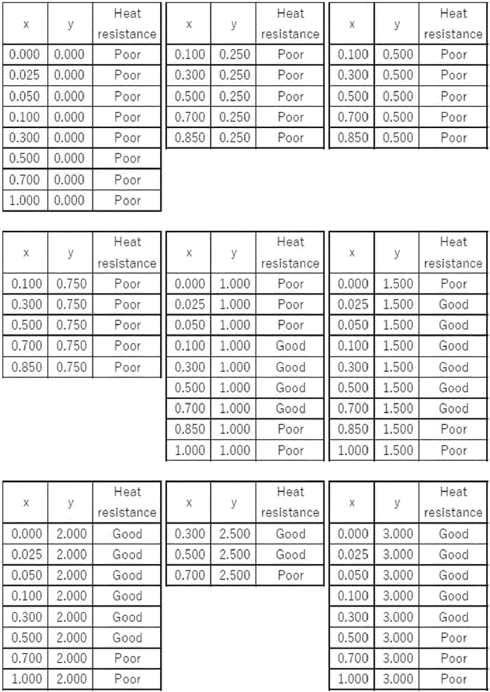
- Table 1 below is a plot showing experimental results of heat resistance in some perovskite-type compounds.
- the evaluation of the heat resistance is clearly indicated for each composition of the perovskite-type compound (values of x and y).
- the evaluation of "good” in heat resistance is defined by the fact that a perovskite structure is confirmed before heating in the X-ray diffraction peak described above, and the deviation ( ⁇ 2 ⁇ ) of peak positions before heating and after heating is 0.05° or less.
- the evaluation of "poor” in heat resistance is defined by the fact that a perovskite structure is not confirmed in the X-ray diffraction peak before heating, or the deviation ( ⁇ 2 ⁇ ) of the peak position of the X-ray diffraction peak before and after heating is larger than 0.05°.
- Fig. 6 is a plot showing experimental results of heat resistance in some perovskite-type compounds.
- Fig. 6 is a diagram showing the experimental results shown in Table 1.
- the horizontal axis represents the value of x in the composition formula
- the vertical axis represents the value of y in the composition formula.
- the evaluation "good” in the heat resistance is indicated by " ⁇ ”
- the evaluation "poor” in the heat resistance is indicated by " ⁇ ”.
- the region having high heat resistance extends from a region where x is approximately middle and y is middle to a region where x is small and y is large.
- y is preferably a desired value or more and 3 or less.
- the value of y is also preferably middle. As x is larger than a middle value, the range of values that y can take is narrower.
- a perovskite-type compound having higher heat resistance can be obtained more reliably, when x and y preferably belong to any of the following ranges (1) to (5).
Landscapes
- Chemical & Material Sciences (AREA)
- Organic Chemistry (AREA)
- Life Sciences & Earth Sciences (AREA)
- Engineering & Computer Science (AREA)
- Chemical Kinetics & Catalysis (AREA)
- General Chemical & Material Sciences (AREA)
- Geochemistry & Mineralogy (AREA)
- Materials Engineering (AREA)
- Inorganic Chemistry (AREA)
- Photovoltaic Devices (AREA)
Abstract
Provided is a perovskite-type compound having high heat resistance. The perovskite-type compound comprising a composition represented by A(Pb1-xSnx)I3-yBry. The element A is one kind or two or more kinds of elements selected from the group consisting of Li, Na, K, Rb and Cs. In the composition formula, x and y belong to any of ranges (1) to (6) below: (1) 0.0 ≤ x < 0.0125 and 1.6 ≤ y ≤ 3.0; (2) 0.0125 ≤ x < 0.1 and 1.1 ≤ y ≤ 3.0; (3) 0.1 ≤ x < 0.3 and 0.8 ≤ y ≤ 3.0; (4) 0.3 ≤ x < 0.5 and 0.8 ≤ y ≤ 3.0; (5) 0.5 ≤ x < 0.7 and 0.8 ≤ y ≤ 2.8; and (6) 0.7 ≤ x ≤ 0.8 and 0.8 ≤ y ≤ 1.8.
Description
- The present invention relates to a perovskite-type compound and a photoelectric conversion element.
- In recent years, as one of next-generation solar cells, a photoelectric conversion element (for example, a perovskite solar cell) containing a compound having a perovskite structure (perovskite-type compound) has attracted attention. As an example, the perovskite solar cell has a so-called n-i-p type laminated structure in which an electron transport layer made of an n-type semiconductor, a perovskite layer (light absorbing layer), and a hole transport layer made of a p-type semiconductor are arranged in this order from the light-receiving side. As another example, the perovskite solar cell has a so-called p-i-n type laminated structure in which a hole transport layer made of a p-type semiconductor, a perovskite layer, and an electron transport layer made of an n-type semiconductor are arranged in this order from the light-receiving side.
- The perovskite layer contains a compound having a perovskite type crystal structure. The compound having the perovskite-type crystal structure is represented by the general formula A-B-X3.
- It is known that a wide variety of elements or molecules can be applied as the elements or molecules A, B, and X constituting the perovskite-type compound (
Non Patent Literature 1,Non Patent Literature 2, and Non Patent Literature 3). -
- Non Patent Literature 1: Liang, J., et al., J. Am. Chem. Soc. 139, 14009-14012 (2017)
- Non Patent Literature 2: Fang, Z., et al., Nano Energy 61, 389-396 (2019)
- Non Patent Literature 3: Wang, Z., et al., Adv. Sci. 2019, 6, 1801704
- However, it is known that many perovskite-type compounds applied to photoelectric conversion elements have problems in terms of heat resistance. In particular, in the case of being used for a space such as a satellite under an environment that can be exposed to high temperatures, a perovskite-type compound that can withstand higher temperatures than those used on the ground is required.
- From such a viewpoint, a perovskite-type compound and a photoelectric conversion element having high heat resistance are desired.
- In one aspect, a perovskite-type compound comprises a composition represented by A(Pb1-xSnx)I3-yBry. The element A is one kind or two or more kinds of elements selected from the group consisting of Li, Na, K, Rb and Cs. x and y in the composition formula belong to any of ranges (1) to (6) below:


- In one aspect, a photoelectric conversion element comprises a light absorbing layer including the above-mentioned perovskite-type compound.
-
-
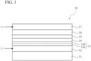
Fig. 1 is a thickness direction cross-sectional view illustrating an example of a photoelectric conversion element according to an embodiment. -
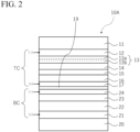
Fig. 2 is a thickness direction cross-sectional view illustrating another example of the photoelectric conversion element according to the embodiment. -
Fig. 3 is a diagram showing a band gap of a perovskite-type compound comprising a composition represented by Cs(Pb1-xSnx)I3-yBry. -
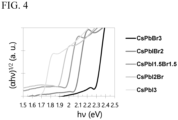
Fig. 4 is a Tauc plot of absorption coefficients in some perovskite-type compounds. -
Fig. 5 is a graph showing results of X-ray diffraction experiments for some perovskite-type compounds. -
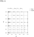
Fig. 6 is a plot showing experimental results of heat resistance in some perovskite-type compounds. - Hereinafter, embodiments will be described with reference to the drawings. In the following drawings, the same or similar parts are denoted by the same or similar reference numerals. However, it should be noted that the drawings are schematic, and ratios of dimensions and the like may be different from actual ones.
-
Fig. 1 is a thickness direction cross-sectional view illustrating an example of a photoelectric conversion element according to an embodiment. The photoelectric conversion element shown inFig. 1 may be a perovskite-type solar cell including a light absorbing layer that comprises a compound having a perovskite structure. The photoelectric conversion element illustrated inFig. 1 is a so-called single-junction photoelectric conversion element. - The
photoelectric conversion element 10 may include asubstrate 11, a firstconductive layer 12, anelectron transport layer 13, alight absorbing layer 14, ahole transport layer 15, a secondconductive layer 16, and a thirdconductive layer 17. The firstconductive layer 12 is provided on thesubstrate 11. Theelectron transport layer 13 is provided on the firstconductive layer 12. Thelight absorbing layer 14 is provided on theelectron transport layer 13. Thehole transport layer 15 is provided on thelight absorbing layer 14. The secondconductive layer 16 is provided on thehole transport layer 15. The thirdconductive layer 17 is provided on the secondconductive layer 16. - The
substrate 11 is a base for laminating the firstconductive layer 12, theelectron transport layer 13, thelight absorbing layer 14, thehole transport layer 15, the secondconductive layer 16 and the thirdconductive layer 17. Thesubstrate 11 can be selected from a transparent glass substrate such as soda-lime glass or alkali-free glass, a resin substrate, a metal substrate, a ceramic substrate, and the like. Thesubstrate 11 may be either a substrate having no translucency or a substrate having translucency. Thesubstrate 11 may be a flexible substrate. - In the present specification, "translucency" means that 10% or more of light having any wavelength of 200 nm to 2000 nm is transmitted.
- When the
substrate 11 has translucency, light may enter toward thephotoelectric conversion element 10 from thesubstrate 11 side (lower side in the drawing) or from the thirdconductive layer 17 side (upper side in the drawing). On the other hand, when thesubstrate 11 does not have translucency, light enters thephotoelectric conversion element 10 from the thirdconductive layer 17 side (upper side in the drawing). - Details of the first
conductive layer 12, theelectron transport layer 13, thelight absorbing layer 14, thehole transport layer 15, the secondconductive layer 16, and the thirdconductive layer 17 are described later. -
Fig. 2 is a thickness direction cross-sectional view illustrating another example of the photoelectric conversion element according to the embodiment. The photoelectric conversion element shown inFig. 2 may be a perovskite-type solar cell including a light absorbing layer that comprises a compound having a perovskite structure. The photoelectric conversion element illustrated inFig. 2 is a so-called multi-junction photoelectric conversion element. A multi-junction photoelectric conversion element includes a plurality of photoelectric conversion cells laminated on each other. That is, the multi-junction photoelectric conversion element may include a plurality of light absorbing layers. - In
Fig. 2 , thephotoelectric conversion element 10A has a laminated structure in which a top cell TC and a bottom cell BC are laminated on each other. In the configuration ofFig. 2 , light enters thephotoelectric conversion element 10A from the top cell TC side (upper side in the drawing). Among the incident light, light on a short wavelength side is photoelectrically converted by the top cell TC. Further, among the incident light, light on the long wavelength side that has passed through the top cell TC is photoelectrically converted by the bottom cell BC. - The top cell TC may have the same configuration as the perovskite-type photoelectric conversion element shown in
Fig. 1 . Therefore, the top cell TC may include thesubstrate 11, the firstconductive layer 12, theelectron transport layer 13, thelight absorbing layer 14, thehole transport layer 15, the secondconductive layer 16, and the thirdconductive layer 17. The firstconductive layer 12 is provided on thesubstrate 11. Theelectron transport layer 13 is provided on the firstconductive layer 12. Thelight absorbing layer 14 is provided on theelectron transport layer 13. Thehole transport layer 15 is provided on thelight absorbing layer 14. The secondconductive layer 16 is provided on thehole transport layer 15. The thirdconductive layer 17 is provided on the secondconductive layer 16. Here, thesubstrate 11 is a substrate having translucency. - The bottom cell BC may include a
substrate 20, afirst electrode layer 21, a photoelectric conversion layer (light absorbing layer) 22, abuffer layer 23, and asecond electrode layer 24. Thefirst electrode layer 21 may be provided on thesubstrate 20. Thephotoelectric conversion layer 22 may be provided on thefirst electrode layer 21. Thebuffer layer 23 may be provided on thephotoelectric conversion layer 22. Thesecond electrode layer 24 may be provided on thebuffer layer 23. - As the bottom cell BC, for example, a configuration of a known photoelectric conversion element (for example, a solar cell) such as a compound photoelectric conversion element such as a CZTS photoelectric conversion element, a CIGS photoelectric conversion element, a CdTe photoelectric conversion element, or a GaAs photoelectric conversion element, or a silicon photoelectric conversion element or an organic photoelectric conversion element can be applied. Therefore, any explanation regarding the configuration of the bottom cell BC is omitted. The
buffer layer 23 of the bottom cell BC may be omitted. - The
photoelectric conversion element 10A illustrated inFig. 2 has a so-called four-terminal tandem structure including four terminals including two positive electrodes and two negative electrodes. In this case, thephotoelectric conversion element 10A may have anintermediate layer 19 between the top cell TC and the bottom cell BC. Theintermediate layer 19 may be a transparent insulating layer. - Instead of the four-terminal tandem structure illustrated in
Fig. 2 , the photoelectric conversion element may have a two-terminal tandem structure. In this case, the photoelectric conversion element may not include at least the secondconductive layer 16, the thirdconductive layer 17, and thesecond electrode layer 24 illustrated inFig. 2 . - Next, the first
conductive layer 12, theelectron transport layer 13, thelight absorbing layer 14, thehole transport layer 15, the secondconductive layer 16, and the thirdconductive layer 17 described above are described in detail. - The first
conductive layer 12 may be a layer that acts as an anode of the photoelectric conversion element. Examples of the material of the firstconductive layer 12 include: conductive transparent materials such as copper iodide (CuI), indium tin oxide (ITO), tin oxide (SnO2), fluorine doped tin oxide (FTO), aluminum doped zinc oxide (AZO), indium zinc oxide (IZO), and gallium doped zinc oxide (GZO); metal sodium; a sodium-potassium alloy; metal lithium; metal magnesium; metal aluminum; a magnesium-silver mixture; a magnesium-indium mixture; an aluminum-lithium alloy; an aluminum-aluminum oxide (Al/Al2O3) mixture; and an aluminum-lithium fluoride (Al/LiF) mixture. The above materials may be used singly or as a mixture of two or more kinds thereof. - The first
conductive layer 12 preferably has translucency. However, when light enters the photoelectric conversion element from the thirdconductive layer 17 side, the firstconductive layer 12 may not have translucency. - The first
conductive layer 12 can be formed by, for example, a film forming method such as a vapor deposition method or a sputtering method. Although not particularly limited, the thickness of the firstconductive layer 12 is preferably 0.1 µm or more. Accordingly, sufficient conductivity can be maintained in the firstconductive layer 12. Although not particularly limited, the thickness of the firstconductive layer 12 is preferably 5.0 µm or less. This makes it easy to maintain the light transmittance of the firstconductive layer 12 relatively high. - The
electron transport layer 13 has a function of transporting electrons generated by photoexcitation of thelight absorbing layer 14 to the firstconductive layer 12. Therefore, theelectron transport layer 13 is preferably formed of a material having characteristics in which electrons generated in thelight absorbing layer 14 can easily move to theelectron transport layer 13 and in which electrons of theelectron transport layer 13 can easily move to the firstconductive layer 12. - Examples of the material of the
electron transport layer 13 include inorganic materials such as titanium oxide (TiO2), tungsten oxide (WO2, WO3, W2O3, etc.), zinc oxide (ZnO), niobium oxide (Nb2O5 and the like), tantalum oxide (Ta2O5 and the like), yttrium oxide (Y2O3 and the like), strontium titanate (SrTiO3 and the like) and tin oxide (SnO2), and organic materials such as fullerene (C60, C70, etc.) and derivatives thereof (PC60BM, PC70BM, ICBA, Hydrogenated C60, Hydroxylated C60, etc.). The above materials may be used alone, or may be a mixture of two or more kinds. - The
electron transport layer 13 may have a single layer structure or a laminated structure including a plurality of layers. InFigs. 1 and2 , theelectron transport layer 13 includes adense layer 13a having a dense structure and aporous layer 13b having a porous structure. Thedense layer 13a is positioned between the firstconductive layer 12 and theporous layer 13b, and theporous layer 13b is positioned between thedense layer 13a and thelight absorbing layer 14. - The
dense layer 13a has a denser structure than theporous layer 13b. In other words, the number of voids in thedense layer 13a is smaller than the number of voids in theporous layer 13b. Thedense layer 13a is a layer in which a solution or the like used for forming thelight absorbing layer 14 hardly infiltrates. Thedense layer 13a has a function of preventing contact between the firstconductive layer 12 and the secondconductive layer 16 and has a function of preventing contact between the firstconductive layer 12 and thehole transport layer 15, the contacts causing a decrease in photovoltaic power. Therefore, reduction in photovoltaic power can be suppressed by thedense layer 13a. - The thickness of the
dense layer 13a is, for example, preferably in the range of 5 nm to 200 nm, and more preferably in the range of 10 nm to 100 nm. - As an example, when the
electron transport layer 13 is titanium oxide, thedense layer 13a can be formed by the following method. First, a coating liquid containing a titanium chelate compound is prepared, and the coating liquid is coated onto the firstconductive layer 12 by a film forming method such as a spin coating method, a screen printing method, a spray pyrolysis method, or an aerosol deposition method. Thereafter, thedense layer 13a containing titanium oxide is formed by firing. After the firing, thedense layer 13a containing titanium oxide may be immersed in an aqueous solution of titanium tetrachloride. Thus, the denseness of thedense layer 13a can be increased. The titanium chelate compound used for forming thedense layer 13a containing titanium oxide is preferably a compound having an acetoacetic acid ester chelate group, a compound having a β-diketone chelate group, or the like. - On the other hand, the
porous layer 13b has larger voids than thedense layer 13a, and is a layer into which a solution or the like used for forming thelight absorbing layer 14 infiltrates. The material of thelight absorbing layer 14 can be filled in and held in the pores of theporous layer 13b. Therefore, theporous layer 13b has a function of expanding a contact area between theelectron transport layer 13 and thelight absorbing layer 14 and has a function of efficiently transferring electrons generated by photoexcitation in thelight absorbing layer 14 to theelectron transport layer 13. As a result, electrons generated by photoexcitation in thelight absorbing layer 14 can be efficiently charge separated by theporous layer 13b, and recombination of electrons and holes can be suppressed. As a result, the photoelectric conversion efficiency of the solar cell can be improved. - The thickness of the
porous layer 13b is, for example, preferably in a range of 10 nm to 2000 nm, and more preferably in a range of 20 nm to 500 nm. - As an example, when the
electron transport layer 13 is formed of titanium oxide, theporous layer 13b can be formed by the following method. First, for example, a coating liquid containing titanium oxide particles is prepared, and the coating liquid is coated onto thedense layer 13a by a film forming method such as a spin coating method, a screen printing method, a spray pyrolysis method, or an aerosol deposition method. Thereafter, theporous layer 13b containing titanium oxide is formed by firing. Although not particularly limited, when theporous layer 13b is formed of titanium oxide, anatase type titanium oxide particles are preferably used. - The
hole transport layer 15 is positioned between the light absorbinglayer 14 and the secondconductive layer 16. Thehole transport layer 15 has a function of capturing holes generated in thelight absorbing layer 14 and has a function of moving the holes to the secondconductive layer 16 as a cathode. Thehole transport layer 15 may contain a matrix component composed of, for example, 2,2',7,7'-tetrakis-(N,N-di-p-methoxyphenylamine)9,9'-spirobifluorene (Spiro-OMeTAD) or poly[bis(4-phenyl) (2,4,6-trimethylphenyl)amine] (PTAA), or may contain an organic low molecular weight thin film that preferentially captures holes such as [2-(9Hcarbazol-9-yl)ethyl] phosphonic acid (2PACz). Optionally, in order to suppress recombination of holes and electrons, a passivate layer (not illustrated) made of a metal oxide or an organic thin film may be provided between the light absorbinglayer 14 and thehole transport layer 15. - The
hole transport layer 15 may contain an additive that increases the carrier density. As an example, lithium(fluorosulfonyl) (trifluoromethyl)imide (LiTFSI) can be applied as the additive. - The thickness of the
hole transport layer 15 is preferably in a range of 1 nm to 500 nm, and more preferably in a range of 1 nm or more and 130 nm or less. - The
hole transport layer 15 may be an amorphous layer. In addition, thehole transport layer 15 may contain an organic binder resin or a plasticizer, and the like. - The
hole transport layer 15 can be formed by, for example, the following manufacturing method. First, a compound of said matrix component is dissolved in an organic solvent to prepare a coating liquid, and the coating liquid is coated onto the light absorbing layer 14 (or the passivate layer). Thereafter, the organic solvent is removed to form thehole transport layer 15. The organic solvent used for forming thehole transport layer 15 is preferably a solvent that does not disturb the crystal structure of the organic-inorganic hybrid compound because the organic solvent is coated onto thelight absorbing layer 14. Examples of the solvent include chlorobenzene, toluene and isopropanol, and so on. The coating method of the coating liquid is not particularly limited, and examples thereof include a spin coating method, a screen printing method, and a dip coating method. - The second
conductive layer 16 is a transparent conductive layer having translucency, and acts as an cathode of the photoelectric conversion element. The secondconductive layer 16 is formed on thehole transport layer 15 and is in contact with thehole transport layer 15. - As the material of the second
conductive layer 16, any conductive transparent material can be used. The material of the secondconductive layer 16 is preferably a metal oxide containing, for example, any of indium, zinc and tin. Examples of the material of the secondconductive layer 16 include conductive transparent materials and conductive transparent polymers such as copper iodide (CuI), indium tin oxide (ITO), tin oxide (SnO2), fluorine-doped tin oxide (FTO), aluminum-doped zinc oxide (AZO), indium zinc oxide (IZO), and gallium-doped zinc oxide (GZO). - Optionally, a buffer layer (not illustrated) may be formed between the second
conductive layer 16 and thehole transport layer 15. The buffer layer may be formed of, for example, molybdenum oxide or the like. - The third
conductive layer 17 is an auxiliary electrode layer laminated on the secondconductive layer 16. The thirdconductive layer 17 has a function of reducing electric resistance of a whole cathode. The thirdconductive layer 17 may be a transparent electrode or a collecting electrode such as a metal grid. When the thirdconductive layer 17 is a transparent electrode, the material thereof may be the same as the material of the secondconductive layer 16 or different from the material of the secondconductive layer 16. - Examples of the material of the third
conductive layer 17 include: metal materials such as gold, silver, copper, aluminum and nickel; conductive transparent materials; and conductive transparent polymers such as copper iodide (CuI), indium tin oxide (ITO), tin oxide (SnO2), fluorine-doped tin oxide (FTO), aluminum-doped zinc oxide (AZO), indium zinc oxide (IZO), and gallium-doped zinc oxide (GZO). The above materials may be used singly or as a mixture of two or more kinds thereof. - The third
conductive layer 17 can be produced, for example, by forming a film of an anode material on the secondconductive layer 16 by a method such as vapor deposition or printing. In addition, the thirdconductive layer 17 may be formed in a mesh shape or a grid shape using a vapor deposition mask or the like. - The
light absorbing layer 14 contains a compound having a perovskite structure (perovskite-type compound), and has a function of generating electrons and holes by absorption of incident light. In thelight absorbing layer 14, low-energy electrons in a substance constituting the light absorbing layer are photoexcited by incident light, and higher-energy electrons and holes are generated. Electrons generated by photoexcitation move to theelectron transport layer 13, and holes generated by photoexcitation move to thehole transport layer 15. - The perovskite-type compound is represented by the composition formula A-B-X3. The element A is disposed at each vertex of the unit cell. The element B is disposed near each body center of the unit cell. The element X is disposed near each face center of the unit cell.
- The element A in the composition formula is one kind or two or more kinds of elements selected from the group consisting of lithium (Li), sodium (Na), potassium (K), rubidium (Rb) and cesium (Cs). Preferably, the element A is cesium.
- In the present embodiment, the element B in the composition formula contains lead (Pb) or tin (Sn), or both of lead and tin. The element X in the composition formula is iodine (I) or both iodine (I) and bromine (Br). Therefore, in the present embodiment, the perovskite-type compound has the following composition formula: A(Pb1-x Snx)I3-yBry.
- x in the composition formula is a real number of 0 or more and 1 or less. y in the composition formula is a real number of 0 or more and 3 or less. A more specific range of x and y is described later. Since the perovskite-type compound having the present composition formula does not contain organic molecules, the perovskite-type compound tends to have high heat resistance.
- The perovskite-type compound can be formed by coating a perovskite precursor solution and firing the solution. Here, the perovskite precursor solution may be a mixture obtained by mixing the A-Pb-I3 solution, the A-Pb-Br3 solution, the A-Sn-I3 solution and the A-Sn-Br3 solution in desired amounts. By changing the mixing ratio of these solutions, the values of x and y in the composition formula of the perovskite-type compound described above can be appropriately set. The method for coating the perovskite precursor solution is not particularly limited, but a spin coating method, a screen printing method, a dip coating method, or the like can be coated.
- In the present embodiment, from the viewpoint of the heat resistance of the perovskite-type compound, x and y in the composition formula belong to any one of the following ranges (1) to (6).


- From the viewpoint of the heat resistance of the perovskite-type compound, more preferable ranges of x and y in the composition formula are as follows. In a range where "0.0 ≤ x < 0.0125" is satisfied, "1.8 ≤ y ≤ 3.0" is preferably satisfied, and "2.0 ≤ y ≤ 3.0" is more preferably satisfied.
- In a range where "0.125 ≤ x < 0.1" is satisfied, "1.2 ≤ y ≤ 3.0" is preferably satisfied, "1.3 ≤ y ≤ 3.0" is more preferably satisfied, "1.4 ≤ y ≤ 3.0" is still preferably satisfied, and "1.5 ≤ y ≤ 3.0" is still more preferably satisfied.
- In a range where "0.1 ≤ x < 0.3" is satisfied, "0.9 ≤ y ≤ 3.0" is preferably satisfied, and "1.0 ≤ y ≤ 3.0" is more preferably satisfied.
- In a range where "0.3 ≤ x < 0.5" is satisfied, y is preferably 0.8 or more, more preferably 0.9 or more, and still preferably 1.0 or more. In a range where "0.3 ≤ x < 0.5" is satisfied, y is preferably 2.8 or less, more preferably 2.7 or less, still preferably 2.6 or less, and still more preferably 2.5 or less.
- In a range where "0.5 ≤ x < 0.7" is satisfied, y is preferably 0.8 or more, more preferably 0.9 or more, and still preferably 1.0 or more. In a range where "0.5 ≤ x < 0.7" is satisfied, y is preferably 2.6 or less, more preferably 2.4 or less, still preferably 2.2 or less, and still more preferably 1.8 or less. Furthermore, in a range where "0.5 ≤ x < 0.7" is satisfied, y may be 1.5 or less.
- In a range where "0.7 ≤ x ≤ 0.8" is satisfied, y is preferably 0.8 or more, more preferably 0.9 or more, and still preferably 1.0 or more. In a range where "0.7 ≤ x ≤ 0.8" is satisfied, y is preferably 1.7 or less, more preferably 1.6 or less, and still preferably 1.5 or less.
- In a preferred embodiment, from the viewpoint of the heat resistance of the perovskite-type compound, x and y in the composition formula belong to any of the following ranges (1) to (5).



- It is considered that the perovskite-type compound has high heat resistance in the above ranges of x and y. Specifically, the X-ray diffraction experiment was performed before heating the perovskite-type compound and after heating the perovskite-type compound at 150°C. In the X-ray diffraction pattern of the perovskite-type compound in the above range of x and y, the peak of a diffraction angle (2θ) of 13 to 16° that indicates the perovskite-type compound hardly changes before and after heating. This suggests that the perovskite-type compound can withstand a high temperature of 150°C.
- Preferably, the position of the X-ray diffraction peak at which the diffraction angle 2θ of the perovskite-type compound after being heated for 500 hours under a nitrogen atmosphere at 150°C is found to be 13 to 16° is positioned within a range of 0.05° from the position of the X-ray diffraction peak of the perovskite-type compound before being heated. In this case, the crystal structure of the perovskite-type compound is maintained for a long time under a high temperature condition of 150°C.
- From the viewpoint of the efficiency of pair generation of electrons and holes by sunlight, the band gap (Eg) between the valence band and the conduction band in the perovskite-type compound is desirably smaller than a desired value. From this viewpoint, the band gap is preferably 1.9 eV or less, and more preferably 1.8 eV or less.
- Similarly, from the viewpoint of efficiency in photoelectric conversion, the band gap between the valence band and the conduction band in the perovskite-type compound is preferably 1.5 eV or more, more preferably 1.6 eV or more, and still more preferably 1.7 eV or more. The perovskite-type compound having these band gaps is suitably used as a light absorbing layer of a photoelectric conversion element.
- In particular, in the case of the multi-junction photoelectric conversion element described above, the band gap of the light absorbing layer of the top cell is preferably 1.6 eV to 1.9 eV, and more preferably 1.7 eV to 1.8 eV. In this case, it is known that the photoelectric conversion efficiency of the entire multi-junction photoelectric conversion element is extremely high (see Non Patent Literature 3). Therefore, the band gap of the perovskite-type compound according to the present embodiment is preferably 1.6 eV to 1.9 eV, more preferably 1.7 eV to 1.8 eV.
-
Fig. 3 is a diagram showing a band gap (energy gap) of a perovskite-type compound having a composition formula represented by Cs(Pb1-xSnx)I3-yBry. InFig. 3 , the horizontal axis represents the value of x in the composition formula, and the vertical axis represents the value of y in the composition formula. - Each line drawn in the diagram means a location where the energy gap (Eg) of the perovskite-type compound corresponds to 1.4 eV, 1.5 eV, 1.6 eV, 1.7 eV, 1.8 eV, 1.9 eV, 2.0 eV, 2.1 eV or 2.2 eV, respectively. The region between adjacent lines corresponds to a region having an energy gap of value between the values of the two energy gaps indicated by the respective lines. Therefore, the region between the line labeled as "Eg = 1.7 eV" and the line labeled as "Eg = 1.8 eV" means that the energy gap is in the range of 1.7 eV to 1.8 eV.
- The energy gap illustrated in
Fig. 3 can be calculated by using an absorption coefficient α measured by ultraviolet-visible spectroscopy. The absorption coefficient α can be measured and calculated by ultraviolet-visible spectroscopy, for example, by a method in accordance with JISK0115:2020. The absorption coefficient α actually measured by ultraviolet-visible spectroscopy may vary depending on the frequency ν of light. - To calculate the energy gap, Tauc plot is generated from the measured extinction absorption coefficient α. The Tauc plot shows the absorption coefficient α with the vertical axis as (hνα)1/n and the horizontal axis as hv (see also
Fig. 4 ). InFig. 4 , Tauc plot of the extinction absorption coefficient α measured by ultraviolet-visible spectroscopy is shown for some perovskite-type compounds. - The band gap Eg of the semiconductor is calculated from the measured absorption coefficient α on the basis of the following relational expression "(hνα)1/n=k(hν-Eg)". "h" is the Planck constant. "v" is the frequency of the emitted light. Since the transition in Cs(Pb1-xSnx)I3-yBry is considered to be a directly permissive transition, "n = 1/2". "k" is a proportional constant.
- In
Fig. 4 , the value of "(hνα)1/2" increases little by little or is maintained almost unchanged as the energy hv of the incident light increases, and draws an ascending curve that sharply increases in the vicinity of the band gap. The value of the energy hv at the intersection of the tangent passing through the inflection point of the steep rising curve and the baseline of the Tauc plot is the band gap Eg. Here, the baseline can be determined by a known method. For example, the baseline may be defined by an approximate straight line obtained by a least squares method from a plurality of measurement points on a sufficiently lower energy side than a sharp rising curve in the vicinity of the band gap. - In this way, the band gap of the perovskite-type compound can be determined. In the present specification, the band gap may be calculated by the above method.
- Referring to
Fig. 3 , in Cs(Pb1-xSnx)I3-yBry, a region having an energy gap of 1.9 eV or less roughly corresponds to a region satisfying "y ≤ 5.0x + 1.0". Therefore, from the viewpoint of photoelectric conversion efficiency in addition to the heat resistance conditions described above, Cs(Pb1-xSnx)I3-yBry more preferably satisfies "y ≤ 5.0x + 1.0". - Further, referring to
Fig. 3 , it is found that the energy gap is 1.6 eV or more when "2.5x + 0.25 ≤ y". Therefore, from the viewpoint of photoelectric conversion efficiency in addition to the heat resistance conditions described above, Cs(Pb1-xSnx)I3-yBry more preferably satisfies "2.5x + 0.25 ≤ y". - Next, experimental results on the heat resistance of the perovskite-type compound of the above embodiment are described. In the experimental example, the perovskite-type compound was produced by the following procedure.
- First, a CsPbI3 solution at a concentration of 0.4M (molar), a CsPbBr3 solution at the same concentration, a CsSnI3 solution at the same concentration, and a CsSnBr3 solution at the same concentration were prepared. The solvent is dimethyl sulfoxide (DMSO).
- Next, some or all of the CsPbI3 solution, the CsPbBr3 solution, the CsSnI3 solution and the CsSnBr3 solution were mixed in a desired ratio as necessary according to the composition ratio of the elements constituting the perovskite-type compound to be produced. Thereby, Cs(Pb1-x Snx)I3-yBry solution having desired values of x and y was prepared.
- Next, Cs(Pb1-xSnx)I3-yBry solution was coated onto the glass substrate cleaned in advance by a spin coating method in a nitrogen atmosphere. The spin coating was performed under the conditions of 0 rpm for the first 10 seconds, 500 rpm for the next 10 seconds, and 2000 rpm for the next 80 seconds. When 80 seconds had elapsed from the start of spin coating, 0.15 ml of toluene was used as a poor solvent.
- Next, the solution coated onto the glass substrate was sintered to form a thin film of the perovskite-type compound. The sintering was performed at a temperature of 300°C for 2 minutes. As shown in Table 1 below, thin films of a large number of perovskite-type compounds in which the combination of x and y in the composition formula was changed were produced.
- An experiment on heat resistance was conducted for the thin film of the perovskite-type compound produced. First, an X-ray diffraction experiment was performed on the thin film of the perovskite-type compound (before heating at 150°C) to measure the position (2θ) of the X-ray diffraction peak of the perovskite-type compound. The position of the X-ray diffraction peak is defined by the position of the local maximum value of the intensity.
- Next, the thin film of the perovskite-type compound was placed on the heater together with the glass substrate, and was heated at 150°C for 500 hours under a nitrogen atmosphere. Then, an X-ray diffraction experiment was performed on the thin film of the perovskite-type compound after heating, and the position of the X-ray diffraction peak of the perovskite-type compound was measured.
-
Fig. 5 is a graph showing results of X-ray diffraction experiments for some perovskite-type compounds. InFig. 5 , the result of the X-ray diffraction experiment on the perovskite-type compound before heating is indicated by a broken line. InFig. 5 , the result of the X-ray diffraction experiment on the perovskite-type compound after heating is shown by a solid line. From the graph shown inFig. 5 , it can be seen that in some compounds, an X-ray diffraction peak derived from a perovskite structure in which a diffraction angle 2θ is observed at 13 to 16° from a state before heating is not observed. This is considered to be because the corresponding composition (corresponding to specific values of x and y) is very unstable, and the perovskite structure cannot be maintained at room temperature. In some perovskite-type compounds, the position of the X-ray diffraction peak derived from the perovskite structure in which the diffraction angle 2θ is found to be 13 to 16° varies before and after heating. This is considered to be because the perovskite compound having the corresponding composition was decomposed or phase-separated by heating. In other words, when there is an X-ray diffraction peak derived from the perovskite structure in which the diffraction angle 2θ is found to be 13 to 16° before heating, and when the peak position hardly varies before and after heating, it can be said that the perovskite-type compound has heat resistance of 150°C. - Table 1 below is a plot showing experimental results of heat resistance in some perovskite-type compounds. In the following Table 1, the evaluation of the heat resistance is clearly indicated for each composition of the perovskite-type compound (values of x and y). Here, the evaluation of "good" in heat resistance is defined by the fact that a perovskite structure is confirmed before heating in the X-ray diffraction peak described above, and the deviation (Δ2θ) of peak positions before heating and after heating is 0.05° or less. The evaluation of "poor" in heat resistance is defined by the fact that a perovskite structure is not confirmed in the X-ray diffraction peak before heating, or the deviation (Δ2θ) of the peak position of the X-ray diffraction peak before and after heating is larger than 0.05°.

-
Fig. 6 is a plot showing experimental results of heat resistance in some perovskite-type compounds.Fig. 6 is a diagram showing the experimental results shown in Table 1. InFig. 6 , the horizontal axis represents the value of x in the composition formula, and the vertical axis represents the value of y in the composition formula. InFig. 6 , the evaluation "good" in the heat resistance is indicated by "∘", and the evaluation "poor" in the heat resistance is indicated by "×". - Referring to
Fig. 6 , the region having high heat resistance extends from a region where x is approximately middle and y is middle to a region where x is small and y is large. Specifically, in a section where x is small, y is preferably a desired value or more and 3 or less. In a section where x is middle, the value of y is also preferably middle. As x is larger than a middle value, the range of values that y can take is narrower. - More specifically, in Cs(Pb1-xSnx)I3-yBry, it is presumed from
Fig. 6 that a perovskite-type compound having high heat resistance is obtained, when x and y in the composition formula belong to any of the following ranges (1) to (6).





- It can be understood from
Fig. 6 that a perovskite-type compound having higher heat resistance can be obtained more reliably, when x and y preferably belong to any of the following ranges (1) to (5).


- The range represented by x and y can be a perovskite-type compound having heat resistance at a high temperature of 150°C. Such a perovskite-type compound having resistance to high temperature can be suitably used even when used in an environment that can be exposed to high temperature, for example, for a space such as a satellite.
- In the above embodiment, the configuration example of the perovskite-type solar cell has been described as an example of the photoelectric conversion element. However, the photoelectric conversion element of the present invention may be applied to, for example, a photodiode, an optical sensor, or the like.
- In the above embodiment, the configuration of a single-junction cell as one solar cell and the configuration of a multi-junction solar cell in which two layers of solar cells are laminated were described. However, the configuration of the photoelectric conversion element of the present invention can be similarly applied to a multi-junction solar cell in which three or more layers of solar cells are laminated. In this case, the configuration of the photoelectric conversion element of the present invention is not limited to the top cell, and can be applied to any cell.
- Each feature described in each of the foregoing embodiments may be applied to or replaced with another embodiment as much as possible. In the above embodiment, the thin-film photoelectric conversion element has been described as an example, but the present invention is not limited thereto, and can be applied to a crystalline photoelectric conversion element as much as possible.
- This application claims priority based on
Japanese Patent Application No. 2022-092813 filed on June 8, 2022
Claims (7)
- A perovskite-type compound comprising a composition represented by A(Pb1-x Snx)I3-yBry,wherein element A is one kind or two or more kinds of elements selected from the group consisting of Li, Na, K, Rb and Cs,x and y belong to any of ranges (1) to (6) below:





- The perovskite-type compound according to claim 1,
wherein x and y belong to any of ranges (1) to (5) below:


- The perovskite-type compound according to claim 1 or 2, wherein a band gap between a valence band and a conduction band is 1.9 eV or less.
- The perovskite-type compound according to any one of claims 1 to 3, wherein a band gap between a valence band and a conduction band is 1.5 eV or more.
- The perovskite-type compound according to any one of claims 1 to 4, wherein the element A is Cs.
- The perovskite-type compound according to claim 5, further satisfying "y ≤ 5.0x + 1.0".
- A photoelectric conversion element comprising a light absorbing layer including the perovskite-type compound according to any one of claims 1 to 6.
Applications Claiming Priority (2)
| Application Number | Priority Date | Filing Date | Title |
|---|---|---|---|
| JP2022092813A JP7865483B2 (en) | 2022-06-08 | 2022-06-08 | Perovskite-type compounds and photoelectric conversion elements |
| PCT/JP2023/020980 WO2023238858A1 (en) | 2022-06-08 | 2023-06-06 | Perovskite compound and photoelectric conversion element |
Publications (2)
| Publication Number | Publication Date |
|---|---|
| EP4538232A1 true EP4538232A1 (en) | 2025-04-16 |
| EP4538232A4 EP4538232A4 (en) | 2026-07-15 |
Family
ID=89118357
Family Applications (1)
| Application Number | Title | Priority Date | Filing Date |
|---|---|---|---|
| EP23819838.6A Pending EP4538232A4 (en) | 2022-06-08 | 2023-06-06 | PEROWSKIT CONNECTION AND PHOTOELECTRIC CONVERSION ELEMENT |
Country Status (4)
| Country | Link |
|---|---|
| EP (1) | EP4538232A4 (en) |
| JP (1) | JP7865483B2 (en) |
| CN (1) | CN119255966A (en) |
| WO (1) | WO2023238858A1 (en) |
Family Cites Families (6)
| Publication number | Priority date | Publication date | Assignee | Title |
|---|---|---|---|---|
| US20220277902A1 (en) | 2019-07-31 | 2022-09-01 | The Board Of Regents Of The University Of Oklahoma | Dichalcogenide composite electrode and solar cell and uses |
| KR102303840B1 (en) * | 2019-08-26 | 2021-09-17 | 중앙대학교 산학협력단 | Inorganic perovskite compound, manufacturing method thereof, and solar cell comprising the same |
| JP2021082726A (en) | 2019-11-20 | 2021-05-27 | 国立大学法人電気通信大学 | Quantum dot, optical devices using the same, and manufacturing method for quantum dot |
| CN111253942A (en) | 2020-03-04 | 2020-06-09 | 长春工业大学 | Upconversion nanoluminescent material with perovskite structure, preparation method and application thereof |
| KR102486603B1 (en) * | 2020-09-04 | 2023-01-10 | 경희대학교 산학협력단 | Methods of perovskite-polymer composite particles and perovskite-polymer composite particles prepared thereby |
| JP7590757B2 (en) | 2020-12-11 | 2024-11-27 | ユニパルス株式会社 | Distance measuring circuit, distance measuring device, measuring device and scanning control device |
-
2022
- 2022-06-08 JP JP2022092813A patent/JP7865483B2/en active Active
-
2023
- 2023-06-06 CN CN202380045626.1A patent/CN119255966A/en active Pending
- 2023-06-06 EP EP23819838.6A patent/EP4538232A4/en active Pending
- 2023-06-06 WO PCT/JP2023/020980 patent/WO2023238858A1/en not_active Ceased
Also Published As
| Publication number | Publication date |
|---|---|
| EP4538232A4 (en) | 2026-07-15 |
| JP2023179899A (en) | 2023-12-20 |
| CN119255966A (en) | 2025-01-03 |
| WO2023238858A1 (en) | 2023-12-14 |
| JP7865483B2 (en) | 2026-05-26 |
Similar Documents
| Publication | Publication Date | Title |
|---|---|---|
| Yang et al. | Highly efficient perovskite solar modules by scalable fabrication and interconnection optimization | |
| EP3347502B1 (en) | Formation of lead-free perovskite film | |
| EP3381070B1 (en) | Mixed cation perovskite | |
| Mali et al. | pin/nip type planar hybrid structure of highly efficient perovskite solar cells towards improved air stability: synthetic strategies and the role of p-type hole transport layer (HTL) and n-type electron transport layer (ETL) metal oxides | |
| Niu et al. | Oxygen doping in nickel oxide for highly efficient planar perovskite solar cells | |
| Lyu et al. | Counter electrodes for perovskite solar cells: materials, interfaces and device stability | |
| Liu et al. | Reduced open-circuit voltage loss for highly efficient low-bandgap perovskite solar cells via suppression of silver diffusion | |
| KR20210107529A (en) | Mexin-modified hybrid photoconverter | |
| US20180130913A1 (en) | Semiconductor Film and Semiconductor Element | |
| JP7429881B2 (en) | solar cells | |
| US12520652B2 (en) | Multilayer back contacts for perovskite photovoltaic devices | |
| US20250048822A1 (en) | Photoelectric conversion element and manufacturing method of photoelectric conversion element | |
| US20140060639A1 (en) | Copper oxide core/shell nanocrystals for use in photovoltaic cells | |
| JP7357247B2 (en) | solar cells | |
| Chang et al. | Preparation and characterization of MoSe2/CH3NH3PbI3/PMMA perovskite solar cells using polyethylene glycol solution | |
| EP4665124A1 (en) | Solar cell and preparation method therefor | |
| Jiang et al. | Recent advances of monolithic all‐perovskite tandem solar cells: from materials to devices | |
| Garg et al. | Performance of ZnF e 2 O 4 as a photoabsorber in solution-processed all-oxide planar photovoltaics | |
| Goje et al. | Advancements and challenges in lead-free flexible perovskite solar cells for sustainable energy solutions | |
| EP4084104A1 (en) | Solar cell | |
| WO2021131428A1 (en) | Solar cell | |
| JP7656838B2 (en) | Solar cells and photoelectric conversion elements | |
| WO2023238858A1 (en) | Perovskite compound and photoelectric conversion element | |
| Kartikay et al. | Hole transport layer free stable perovskite solar cell with low temperature processed carbon electrodes | |
| KR102919669B1 (en) | Tandem solar cell device and Manufacturing method thereof |
Legal Events
| Date | Code | Title | Description |
|---|---|---|---|
| STAA | Information on the status of an ep patent application or granted ep patent |
Free format text: STATUS: THE INTERNATIONAL PUBLICATION HAS BEEN MADE |
|
| PUAI | Public reference made under article 153(3) epc to a published international application that has entered the european phase |
Free format text: ORIGINAL CODE: 0009012 |
|
| STAA | Information on the status of an ep patent application or granted ep patent |
Free format text: STATUS: REQUEST FOR EXAMINATION WAS MADE |
|
| 17P | Request for examination filed |
Effective date: 20250107 |
|
| AK | Designated contracting states |
Kind code of ref document: A1 Designated state(s): AL AT BE BG CH CY CZ DE DK EE ES FI FR GB GR HR HU IE IS IT LI LT LU LV MC ME MK MT NL NO PL PT RO RS SE SI SK SM TR |
|
| DAV | Request for validation of the european patent (deleted) | ||
| DAX | Request for extension of the european patent (deleted) | ||
| A4 | Supplementary search report drawn up and despatched |
Effective date: 20260611 |