EP4535634A1 - Electronic control device, gate drive method for power semiconductor element - Google Patents
Electronic control device, gate drive method for power semiconductor element Download PDFInfo
- Publication number
- EP4535634A1 EP4535634A1 EP22943802.3A EP22943802A EP4535634A1 EP 4535634 A1 EP4535634 A1 EP 4535634A1 EP 22943802 A EP22943802 A EP 22943802A EP 4535634 A1 EP4535634 A1 EP 4535634A1
- Authority
- EP
- European Patent Office
- Prior art keywords
- semiconductor element
- power semiconductor
- switching
- voltage
- gate drive
- Prior art date
- Legal status (The legal status is an assumption and is not a legal conclusion. Google has not performed a legal analysis and makes no representation as to the accuracy of the status listed.)
- Pending
Links
Images



Classifications
-
- H—ELECTRICITY
- H02—GENERATION; CONVERSION OR DISTRIBUTION OF ELECTRIC POWER
- H02M—APPARATUS FOR CONVERSION BETWEEN AC AND AC, BETWEEN AC AND DC, OR BETWEEN DC AND DC, AND FOR USE WITH MAINS OR SIMILAR POWER SUPPLY SYSTEMS; CONVERSION OF DC OR AC INPUT POWER INTO SURGE OUTPUT POWER; CONTROL OR REGULATION THEREOF
- H02M1/00—Details of apparatus for conversion
- H02M1/08—Circuits specially adapted for the generation of control voltages for semiconductor devices incorporated in static converters
-
- H—ELECTRICITY
- H03—ELECTRONIC CIRCUITRY
- H03K—PULSE TECHNIQUE
- H03K3/00—Circuits for generating electric pulses; Monostable, bistable or multistable circuits
- H03K3/01—Details
- H03K3/012—Modifications of generator to improve response time or to decrease power consumption
-
- H—ELECTRICITY
- H03—ELECTRONIC CIRCUITRY
- H03K—PULSE TECHNIQUE
- H03K17/00—Electronic switching or gating, i.e. not by contact-making and –breaking
- H03K17/04—Modifications for accelerating switching
- H03K17/042—Modifications for accelerating switching by feedback from the output circuit to the control circuit
- H03K17/04206—Modifications for accelerating switching by feedback from the output circuit to the control circuit in field-effect transistor switches
-
- H—ELECTRICITY
- H03—ELECTRONIC CIRCUITRY
- H03K—PULSE TECHNIQUE
- H03K17/00—Electronic switching or gating, i.e. not by contact-making and –breaking
- H03K17/14—Modifications for compensating variations of physical values, e.g. of temperature
- H03K17/145—Modifications for compensating variations of physical values, e.g. of temperature in field-effect transistor switches
-
- H—ELECTRICITY
- H03—ELECTRONIC CIRCUITRY
- H03K—PULSE TECHNIQUE
- H03K17/00—Electronic switching or gating, i.e. not by contact-making and –breaking
- H03K17/16—Modifications for eliminating interference voltages or currents
- H03K17/161—Modifications for eliminating interference voltages or currents in field-effect transistor switches
- H03K17/165—Modifications for eliminating interference voltages or currents in field-effect transistor switches by feedback from the output circuit to the control circuit
-
- H—ELECTRICITY
- H03—ELECTRONIC CIRCUITRY
- H03K—PULSE TECHNIQUE
- H03K17/00—Electronic switching or gating, i.e. not by contact-making and –breaking
- H03K17/16—Modifications for eliminating interference voltages or currents
- H03K17/161—Modifications for eliminating interference voltages or currents in field-effect transistor switches
- H03K17/165—Modifications for eliminating interference voltages or currents in field-effect transistor switches by feedback from the output circuit to the control circuit
- H03K17/166—Soft switching
- H03K17/167—Soft switching using parallel switching arrangements
-
- H—ELECTRICITY
- H03—ELECTRONIC CIRCUITRY
- H03K—PULSE TECHNIQUE
- H03K17/00—Electronic switching or gating, i.e. not by contact-making and –breaking
- H03K17/51—Electronic switching or gating, i.e. not by contact-making and –breaking characterised by the components used
- H03K17/56—Electronic switching or gating, i.e. not by contact-making and –breaking characterised by the components used by the use, as active elements, of semiconductor devices
- H03K17/687—Electronic switching or gating, i.e. not by contact-making and –breaking characterised by the components used by the use, as active elements, of semiconductor devices the devices being field-effect transistors
Definitions
- the present invention relates to a configuration of an electronic control unit and control thereof, and more particularly to a gate drive circuit and a gate driving method of a power semiconductor element mounted on the electronic control unit.
- ECU electronice control units
- an input processing circuit that processes inputs of sensors and switches, an AD conversion circuit, a microcontroller, a power supply circuit, an output processing circuit, a power semiconductor element, and the like are generally mounted.
- ADAS advanced driver-assistance systems
- a direct current is converted into an alternating current by switching control of a power semiconductor element such as an insulated gate bipolar transistor (IGBT) or a SiC-power metal-oxide-semiconductor field-effect transistor (MOSFET).
- a power semiconductor element such as an insulated gate bipolar transistor (IGBT) or a SiC-power metal-oxide-semiconductor field-effect transistor (MOSFET).
- IGBT insulated gate bipolar transistor
- MOSFET SiC-power metal-oxide-semiconductor field-effect transistor
- PTL 1 discloses "a drive circuit that, during a main discharge period, monotonously increases and sets a command discharge current of a gate of a switching element and switches a switching element to an off state by controlling a gate discharge current to a preset command discharge current, and, during a main charge period, monotonously decreases and sets a command charge current of the gate of the switching element and switches the switching element to an on state by controlling a gate charge current to the preset command charge current.
- the drive circuit described in PTL 1 is characterized in that the drive circuit is driven by monotonically increasing the discharge current during the main discharge period, and monotonically decreasing the charge current during the main charge period.
- This gate drive system is a feedforward type, and is driven at a constant gate current value, which is recorded in a memory in advance, for monotonic increase or monotonic decrease and at a constant time of start or stop for increase or decrease.
- an object of the present invention is to provide a highly reliable and low-loss electronic control unit capable of performing a high-speed switching operation while suppressing a surge voltage during a switching operation of a power semiconductor element in an electronic control unit on which the power semiconductor element is mounted, and a gate driving method of the power semiconductor element.
- the present invention includes: a microcontroller; a power semiconductor element; and a gate drive circuit that generates a gate drive current of the power semiconductor element on the basis of a command from the microcontroller.
- the gate drive circuit detects a change in an output voltage of the power semiconductor element to detect start of on/off operation of switching, increases a gate drive current in a process of the switching in an on state and before reaching a peak voltage, and decreases the gate drive current in a process of the switching in an off state and before reaching the peak voltage.
- the present invention is a gate driving method of a power semiconductor element including: (a) a step of detecting a change in a voltage between a drain terminal and a source terminal of a power semiconductor element to detect start of an on/off operation of switching; (b) a step of increasing a gate drive current in a process of the switching when the power semiconductor element is in an on state and before reaching a peak voltage; and (c) a step of reducing the gate drive current in a process of the switching when the power semiconductor element is in an off state and before reaching the peak voltage.
- the electronic control unit on which the power semiconductor element is mounted it is possible to realize the highly reliable and low-loss electronic control unit capable of performing a high-speed switching operation while suppressing a surge voltage during a switching operation of the power semiconductor element, and a gate driving method of the power semiconductor element.
- the names of the terminals of the power semiconductor element are unified to a gate terminal, a drain terminal, and a source terminal, but in the case of the IGBT, the drain terminal can be read as a collector terminal, and the source terminal can be read as an emitter terminal.
- the IGBT or a SiC-power MOSFET is assumed as the power semiconductor element, it is possible to target all power devices that control switching between on and off by a gate voltage, and a Si-power MOSFET, a GaN-power MOSFET, or the like may be used.
- FIGS. 1 , 4 , and 5 An electronic control unit and a gate driving method of a power semiconductor element according to a first embodiment of the present invention will be described with reference to FIGS. 1 , 4 , and 5 .
- FIG. 1 is a schematic configuration diagram of the electronic control unit of the present embodiment, and mainly illustrates a configuration of a gate drive circuit 1.
- FIGS. 4 and 5 are timing charts at the time of an off operation and at the time of an on operation of the power semiconductor element 20, respectively.
- the electronic control unit of the present embodiment includes, as main components, a microcontroller 10, a power semiconductor element 20, and the gate drive circuit 1.
- a microcontroller 10 a microcontroller 10
- the gate drive circuit 1 an input processing circuit, an AD conversion circuit, a power supply circuit, an output processing circuit, and the like are provided, but are omitted in FIG. 1 .
- FIG. 1 illustrates a configuration diagram for one arm for driving the power semiconductor element 20.
- motor driving is performed by using three phases of upper and lower arms in which the configurations of one arm are connected vertically, and this case is configured by a gate drive circuit of six arms having the same configuration as in FIG. 1 and one microcontroller.
- the operation is the same as the operation of the single-phase arm, and thus, here, the embodiment of the present invention will be described as the operation of one arm.
- the microcontroller 10 outputs a PWM gate drive signal 11 to the gate drive circuit 1.
- the gate drive circuit 1 includes an on-drive current switching unit 32 and an off-drive current switching unit 33 that switch a gate drive current of the power semiconductor element 20, a gate-on drive unit 30 and a gate-off drive unit 31 that drive the power semiconductor element 20 with a set drive current, an output transmission unit 40 connected to a drain terminal 22 of the power semiconductor element 20, a constant voltage generation unit 41 that generates a constant voltage for output detection, an off-filter adjustment unit 43 and an on-filter adjustment unit 44 that filter the voltage of the output detection terminal 42, an output-off detection unit 45 and an output-on detection unit 46 that detect the off-start and the on-start of the power semiconductor element 20, respectively, on the basis of a signal after filtering, and an inter-insulation communication unit 12.
- a signal is transmitted by the inter-insulation communication unit 12 from a low-voltage unit (not illustrated) in which the microcontroller 10 is mounted to a high-voltage unit (not illustrated) in which the gate drive circuit 1 is mounted.
- the gate drive current having been supplied from the gate-on drive unit 30 is stopped. Thereafter, the gate-off drive unit 31 outputs the first off-drive current set from the off-drive current switching unit 33 to start the off-drive of the power semiconductor element 20.
- the voltage of the gate terminal 24 gradually decreases due to the start of the off-drive, and becomes constant near the threshold value of the power semiconductor element 20.
- a voltage hereinafter, referred to as "output voltage" between drain terminal 22 and source terminal 23, which is an output voltage, starts to increase, and switching in an off state is started.
- the output transmission unit 40 connected to the drain terminal 22 detects the increase in the output voltage as a change in the AC voltage.
- the constant voltage generation unit 41 generates a constant DC voltage (for example, 5 V) and biases the output detection terminal 42. As illustrated in FIG. 4 , due to the increase in the output voltage, the voltage of the output detection terminal 42 increases from, for example, 5 V of a constant voltage by AC detection of the increase in the output voltage.
- the off-filter adjustment unit 43 functions to prevent erroneous detection due to noise of the output voltage and to perform delay time adjustment (delay circuit) until switching to the second off-drive current, and filters the voltage of the output detection terminal 42 and transmits the voltage to the output-off detection unit 45.
- the output-off detection unit 45 performs a comparison operation on a reference voltage (for example, 6 V) higher than a constant voltage (for example, 5 V) of the voltage of the output detection terminal 42, and detects that off-switching has started when the voltage of the output detection terminal 42 exceeds 6 V.
- a reference voltage for example, 6 V
- a constant voltage for example, 5 V
- the off-switching is detected only once for each off command of the PWM gate drive signal 11, the result of one detection is latched during the period of one PWM and cleared by a next PWM signal. With this operation, a plurality of detections during one switching can be avoided, and an erroneous switching operation of the gate drive current due to erroneous detection due to switching noise or the like can be prevented.
- the off-switching start is transmitted to the off-drive current switching unit 33 by an off-detection signal 47, and in the off-drive current switching unit 33, the drive current is switched from the first off-drive current to the second off-drive current with a smaller current, and the power semiconductor element 20 is driven via the gate-off drive unit 31. That is, the gate drive current is decreased in the process of the switching in the off state and before reaching a peak voltage. By reducing the gate drive current to the second off-drive current during off-switching, an off-surge voltage can be reduced without changing the switching speed of the output voltage change.
- the off-surge voltage depends on a difference in the type and characteristics of the power semiconductor element 20, or various parameters such as a parasitic inductance and a parasitic capacitance of a bus bar or the like of a power module on which the power semiconductor element 20 is mounted. Therefore, the switching timing of the effective gate drive current reduction is often different for each electronic control unit.
- the off-filter adjustment unit 43 adjusting a time from the change in the output voltage to the switching of the gate drive current, it is possible to adjust the optimum timing of the suppression of the off-surge voltage by the switching of the gate drive current.
- the off-filter adjustment unit 43 may be arranged at any position on a path from the drain terminal 22 to the gate-off drive unit 31, the off-filter adjustment unit is arranged at a preceding stage of the output-off detection unit 45 in the present embodiment since the off-filter adjustment unit has a filter function for eliminating erroneous detection due to noise in signal delay adjustment and output voltage change.
- a signal is transmitted by the inter-insulation communication unit 12 from a low-voltage unit (not illustrated) in which the microcontroller 10 is mounted to a high-voltage unit (not illustrated) in which the gate drive circuit 1 is mounted.
- the gate drive circuit 1 When an on command is transmitted to the gate drive circuit 1, first, the gate drive current having been supplied from the gate-off drive unit 31 is stopped. Next, the first on-drive current set from the on-drive current switching unit 32 is output, and the on-drive of the power semiconductor element 20 is started.
- the voltage of the gate terminal 24 gradually increases due to the start of the on-drive, and becomes constant near the threshold value of the power semiconductor element 20. At this time, the output voltage starts to decrease, and switching in the on state is started.
- the output transmission unit 40 connected to the drain terminal 22 detects the decrease in the output voltage as a change in the AC voltage. As described above, the output transmission unit 40 can detect a change in the output voltage of both the on operation and the off operation of the power semiconductor element 20 in an AC manner.
- the gate drive circuit 1 that drives the power semiconductor element 20 operates at a voltage based on the voltage of the source terminal 23, but on the other hand, the voltage between the drain terminal 22 and the source terminal 22, which is the output voltage of the power semiconductor element 20, becomes a high voltage when the power semiconductor element 20 is off, and thus, a configuration with a high withstand voltage is required for the output transmission unit 40 connected to the drain terminal 22.
- a change in the output voltage of both the on operation and the off operation of the power semiconductor element 20 is transmitted as an AC signal to the output transmission unit 40 by using high withstand voltage capacitive coupling.
- the capacitive coupling an increase and a decrease in the output voltage can be transmitted as an AC signal.
- the output transmission unit 40 transmits a decrease in the output voltage as an AC signal.
- the constant voltage generation unit 41 generates a constant DC voltage (for example, 5 V) and biases the output detection terminal 42.
- the power semiconductor 20 starts the on operation, the output voltage starts to decrease, and the voltage of the output detection terminal 42 decreases from a constant voltage (for example, 5 V) by the output transmission unit 40.
- the on-filter adjustment unit 44 functions to prevent erroneous detection due to noise of the output voltage and to perform delay time adjustment (delay circuit) until switching to the second on-drive current, and filters the voltage of the output detection terminal 42 and transmits the voltage to the output-on detection unit 46.
- the off-filter adjustment unit 43 and the on-filter adjustment unit 44 can be made common.
- the output-on detection unit 46 performs a comparison operation on a reference voltage (for example, 4 V) lower than a constant voltage (for example, 5 V) of the voltage of the output detection terminal 42, and detects that on-switching has started when the voltage of the output detection terminal 42 falls below 4 V.
- a reference voltage for example, 4 V
- a constant voltage for example, 5 V
- the on-switching start When the on-switching start is detected by the output-on detection unit 46, the on-switching start it is transmitted to the on-drive current switching unit 32 by an on-detection signal 48, and in the on-drive current switching unit 32, the drive current is switched from the first on-drive current to the second on-drive current with a larger current, and the power semiconductor element 20 is driven via the gate-on drive unit 30. That is, the gate drive current is increased in the process of the switching in the on state and before reaching a peak voltage.
- the recovery surge voltage of the counter arm is generated by the recovery operation of a reflux diode 21 generated when the current flowing in a forward direction to the reflux diode 21 of the power semiconductor element 20 of the counter arm is turned off, and depends on a difference in characteristics of the reflux diode 21, or various parameters such as parasitic inductance and parasitic capacitance of the bus bar or the like of the power module on which the power semiconductor element 20 and the reflux diode 21 are mounted. Therefore, the switching timing of the effective gate drive current reduction is often different for each electronic control unit.
- the on-filter adjustment unit 44 may be arranged at any position on a path from the drain terminal 22 to the gate-on drive unit 30, the on-filter adjustment unit is arranged at a preceding stage of the output-on detection unit 46 in the present embodiment since the on-filter adjustment unit has a filter function for eliminating erroneous detection due to noise in signal delay adjustment and output voltage change.
- the output-off detection unit 45 and the output-on detection unit 46 detect the start of the off-switching and the start of the on-switching, respectively, and do not need to detect the start of the off-switching and the start of the on-switching at the same time, and thus can be integrated into one.
- the detection voltage is different between the on state and the off state, it is necessary to switch the detection voltage. Therefore, by integrating the gate drive circuit 1 of the present embodiment into one semiconductor integrated circuit, the area of the semiconductor chip can be reduced, which is effective in cost reduction.
- the output transmission unit 40 connected to the drain terminal 22 of the power semiconductor element 20, the constant voltage generation unit 41, the output-off detection unit 45, the output-on detection unit 46, the off-filter adjustment unit 43, and the on-filter adjustment unit 44 can detect the change in the output voltage to detect the start of the on-switching or the start of the off-switching.
- the off-drive current switching unit 33 switches and reduces the drive current from the first off-drive current to the second off-drive current, so that the off-surge voltage of the output voltage can be reduced.
- the off-surge voltage can be reduced, and thus as compared with a case where the present invention is not implemented, the first off-drive current can be increased, the off-switching of the power semiconductor element 20 can be speeded up, and the switching loss in the off-state can be reduced.
- the on-drive current switching unit 32 can increase the gate drive current from the first on-drive current to the second on-drive current. Accordingly, when the gate drive current is increased after the recovery surge voltage generated in the recovery operation of the reflux diode 21 of the counter arm is generated, the switching of the output voltage can be speeded up without increasing the recovery surge voltage, and the on-switching loss can be reduced.
- the present invention it is possible to reduce the switching loss by detecting a change in the output voltage of the power semiconductor element 20 and switching and driving the gate drive current with an excellent timing.
- the junction temperature of the power semiconductor element is lowered by the loss reduction, the chip area of the power semiconductor element can be reduced, and the cost can be reduced.
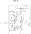
- FIG. 2 is a schematic configuration diagram of the electronic control unit of the present embodiment, and mainly illustrates a configuration of a gate drive circuit 2.
- the gate drive circuit 2 illustrated in FIG. 2 illustrates the configuration of the gate drive circuit 1 of FIG. 1 as a specific circuit example.
- a constant current drive system in which a gate is driven with a constant current
- a constant voltage drive system in which a gate drive current is generated with a drive voltage and a resistor.
- the present embodiment is an embodiment in a case where the present invention is applied to the constant current drive system.
- a command of the PWM gate drive signal 11 transmitted from the microcontroller 10 is transmitted by the inter-insulation communication unit 12 from a low-voltage unit (not illustrated) in which the microcontroller 10 is mounted to a high-voltage unit (not illustrated) in which the gate drive circuit 2 is mounted.
- an on-control switch 74 switches an on-control reference voltage 75 to a power supply voltage VCC 8. Accordingly, an on-control amplifier 73 drives a PMOS FET 66 to control an on-control amplifier negative feedback terminal 72 from the on-control reference voltage 75 to the power supply voltage VCC 8 in a negative feedback operation.
- the gate drive current in the on state determined by the on-control amplifier negative feedback terminal 72 and resistors 64 and 65 becomes 0, and the gate drive current on an on side is turned off.
- the inverter 76 controls an off-control switch 78 connected to the non-inverting input of an off-control amplifier 77, so that the non-inverting input of the off-control amplifier 77 is switched from a level of an off-reference voltage 70 to an off-control reference voltage 81.
- the off-control amplifier 77 drives an NMOS FET 67 to control an off-control amplifier negative feedback terminal 80 from the level of the off-reference voltage 70 to the same voltage as the off-control reference voltage 81 in the negative feedback operation.
- the off-control amplifier negative feedback terminal 80 switches the level of the off-reference voltage 70 to the off-control reference voltage 81, so that the gate drive current in the off-state flows.
- an off-current switching switch 79 is turned on, and an off-current switching switch 84 is turned off, and by the negative feedback control of the off-control amplifier 77, the first off-drive current illustrated in FIG. 4 becomes a current value obtained by dividing the on-control reference voltage 75 by the resistance value of the resistor 69.
- a constant voltage source 54 is a voltage source that outputs a constant voltage, and is assumed to output, for example, 5 V.
- the voltage between the drain terminal 22 and the source terminal 23, which is the output voltage of the power semiconductor element 20 is a constant voltage, so that the voltage of the output detection terminal 42 is the same as that of the constant voltage source 54, and in this case, is 5 V.
- the gate drive current in the off state flows at the timing illustrated in the timing chart of FIG. 4 , whereby the power semiconductor element 20 starts the off operation, and the output voltage of the power semiconductor element 20 increases.
- a capacitance 50 is connected to the drain terminal 22, and increases the voltage of the output detection terminal 42 as the output voltage increases.
- the capacitance 51 has an effect of attenuating the transmission of the output voltage to the output detection terminal 42, and can suppress an excessive voltage change of the output detection terminal 42 when the output voltage has an amplitude of high voltage.
- the increase in the output voltage in the off state is transmitted to the output detection terminal 42, and a delay time Doff for switching the signal to the second off-drive current is adjusted by a resistor 55 and a capacitance 57.
- the resistor 55 and the capacitance 57 also serve as a filter for preventing erroneous detection of noise of the output voltage.
- an off-detection comparator 61 detects an increase in the output voltage, and switches the off-current switching switch 79 from the on state to the off state and the off-current switching switch 84 from the off state to the on state.
- the drive current is switched and reduced from the first off-drive current to the second off-drive current, so that the off-surge voltage of the output voltage can be reduced.
- the off-surge voltage can be reduced, and thus as compared with a case where the present invention is not implemented, the first off-drive current can be increased, the off-switching of the power semiconductor element 20 can be speeded up, and the switching loss in the off-state can be reduced.
- the off-control switch 78 is switched to the off-reference voltage 70 side, so that the gate drive current in the off state is stopped by the negative feedback operation of the off-control amplifier 77.
- the on-control switch 74 is switched from the power supply voltage VCC 8 to the on-control reference voltage 75, and the on-control amplifier negative feedback terminal 72 is controlled to the same voltage as the on-control reference voltage 75 by the negative feedback operation of the on-control amplifier 73, so that the gate drive current on the on side flows.
- an on-current switching switch 63 is turned off, and the on-current switching switch 83 is turned on, and the first on-drive current illustrated in FIG. 5 becomes a current value obtained by dividing the on-control reference voltage 75 by the resistance values of the resistors 64 and 65.
- the power semiconductor element 20 starts the on operation, and the output voltage decreases. As illustrated in FIG. 5 , the decrease in the output voltage is transmitted as the voltage decrease of the output detection terminal 42 via the capacitance 50.
- a delay time Don for switching the signal to the second on-drive current is adjusted by a resistor 56 and a capacitance 58.
- the resistor 56 and the capacitance 58 also serve as a filter for preventing erroneous detection of noise of the output voltage.
- an on-detection comparator 62 detects a decrease in the output voltage, and switches the on-current switching switch 63 from the off state to the on state and switches the on-current switching switch 83 from the on state to the off state. Accordingly, the gate drive current in the on-state is switched to the second on-drive current obtained by dividing the on-control reference voltage 75 by the resistance values of the resistors 64 and 65.
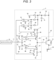
- FIG. 3 is a schematic configuration diagram of the electronic control unit of the present embodiment, and mainly illustrates a configuration of a gate drive circuit 3.
- the gate drive circuit 3 illustrated in FIG. 3 is a constant current drive system similarly to the second embodiment, and is different from the second embodiment in a method of switching between the first on-drive current and the second on-drive current, and the first off-drive current and the second off-drive current.
- Other configurations are similar to those of the second embodiment ( FIG. 2 ).
- the off-detection comparator 61 detects an increase in the output voltage of the power semiconductor element 20, and the off-current switching switch 95 is switched from the on state to the off state. Accordingly, the first off-drive current obtained by dividing the off-control reference voltage 81 by the resistance value of the parallel resistors of the resistors 93 and 94 can be switched to the second off-drive current obtained by dividing the off-control reference voltage 81 by the resistance value of the resistor 93.
- the on-detection comparator 62 detects a decrease in the output voltage of the power semiconductor element 20, and the on-current switching switch 92 is switched from the off state to the on state. Accordingly, the first on-drive current obtained by dividing the on-control reference voltage 75 by the resistance value of the resistor 90 can be switched to the second on-drive current obtained by dividing the on-control reference voltage 75 by the resistance value of the parallel resistors of the resistors 90 and 91.
- the loop of the negative feedback is not switched, and thus the stability of the amplifier is easily obtained.
- FIG. 6 is a schematic configuration diagram of the electronic control unit of the present embodiment, and mainly illustrates a configuration of a gate drive circuit 6.
- the present embodiment is an embodiment in a case where the present invention is applied to the gate drive circuit of the constant voltage drive system.
- a PMOS FET 105 connected to the power supply voltage VCC 8 is turned on, so that the gate drive current in the on state flows due to a differential voltage and a resistor 101 between the power supply voltage VCC 8 and the gate terminal 24.
- an NMOS FET 106 is turned on, so that the gate drive current in the off state flows due to a differential voltage and a resistor 102 between the gate terminal 24 and the off-reference voltage 70.
- the gate can be driven with a simple configuration in which the MOS FET is connected to the gate terminal 24 via the resistor to be turned on and off, and thus the constant voltage drive system is generally widely used.
- the PWM gate drive signal 11 output from the microcontroller 10 is an off command
- a signal is transmitted by the inter-insulation communication unit 12, passes through the inverter 109, and turns off the PMOS FET 105.
- a PMOS FET 104 is also turned off through a NAND 108. Accordingly, the gate drive current in the on state flowing through the PMOS FET 105 and the PMOS FET 104 is turned off.
- the NMOS FET 106 connected to the inverter 109 is turned on, and the NMOS FET 107 is also turned on through an AND 110. Accordingly, the first off-drive current starts to flow, and the off operation of the power semiconductor element 20 is started.
- the operation from the off operation of the power semiconductor element 20 to the off-detection comparator 61 is the same as the operation described in the second and third embodiments.
- the off-drive current is decreased and switched to the second off-drive current by turning off the NMOS FET 107 through the inverters 111 and the AND 110.
- the NMOS FET 106 and the NMOS FET 107 are turned off.
- the PMOS FET 105 is turned on, the first on-drive current determined by the differential voltage and the resistor 101 between the power supply voltage VCC 8 and the gate terminal 24 flows, and the power semiconductor element 20 starts the on operation.
- the operation from the on operation of the power semiconductor element 20 to the on-detection comparator 62 is the same as the operation described in the second and third embodiments.
- the on-detection comparator 62 detects a decrease in the output voltage of the power semiconductor element 20, in addition to the first on-drive current, the current from the PMOS FET 104 increases and the second on-drive current flows by turning on the PMOS FET 104 through the NAND 108.
- the switching loss in the on state can be reduced without increasing the recovery surge voltage of the counter arm, by increasing the gate drive current from the first on-drive current to the second on-drive current.
- FIG. 7 is a diagram illustrating a schematic configuration of the electronic control unit of the present embodiment, and illustrates an example of an inverter on which the gate drive circuit described in any one of the first to fourth embodiments is mounted.
- the electronic control unit is an inverter 126 that converts DC power from a high-voltage battery 120 into three-phase AC power, supplies the three-phase AC power to a motor 121, and performs drive control.
- a power semiconductor element 20B and a reflux diode 21B constituting the upper arm are connected in series to a power semiconductor element 20A and a reflux diode 21A constituting the lower arm, so as constitute a W-phase arm.
- the power semiconductor element 20B and the power semiconductor element 20A are driven and controlled by gate drive currents generated by the gate drive circuits 122B and 122A, respectively.
- the gate drive circuit described in any one of the first to fourth embodiments is used for the gate drive circuits 122B and 122A.
- the gate drive circuits 122B and 122A generate gate drive currents according to the on command and the off command of the PWM gate drive signals 11B and 11A from the microcontroller 10, respectively, and input the gate drive currents to the power semiconductor element 20B and the power semiconductor element 20A.
- arms are configured similarly to the W phase, and the inverter 126 is configured such that the respective arms of the U phase, the V phase, and the W phase are connected in parallel between the high-voltage battery 120 and the motor 121.
- a U-phase output terminal 125, a V-phase output terminal 124, and a W-phase output terminal 123 are connected between the upper and lower arms of the U phase, the V phase, and the W phase, respectively, and are connected to the motor 121.
- the inverter 126 of the present embodiment is configured as described above, and the switching loss of the power semiconductor element mounted inside can be reduced by the gate drive circuit of the present invention, which is effective in improvement of the conversion efficiency of the inverter and improvement of the maximum output power.
- the present invention is not limited to the above-described embodiments, and includes various modifications.
- the above-described embodiments have been described in detail for easy understanding of the present invention, and are not necessarily limited to those having all the described configurations.
- a part of the configuration of a certain embodiment can be replaced with the configuration of another embodiment, and the configuration of another embodiment can be added to the configuration of a certain embodiment.
Landscapes
- Engineering & Computer Science (AREA)
- Power Engineering (AREA)
- Power Conversion In General (AREA)
Abstract
Description
- The present invention relates to a configuration of an electronic control unit and control thereof, and more particularly to a gate drive circuit and a gate driving method of a power semiconductor element mounted on the electronic control unit.
- With the advance of electronic control technology, improvement of the performance of an automobile by electronic control has been achieved in various functions and devices including an engine. In a current automobile, 100 or more electronic control units (ECU) are mounted in many cases, and are important components that control various advanced technologies. These ECUs are required to be small in size and weight, low in cost, and high in efficiency.
- In a broad sense ECU including an ECU, an engine control unit, and an inverter utilized in advanced driver-assistance systems (ADAS), an input processing circuit that processes inputs of sensors and switches, an AD conversion circuit, a microcontroller, a power supply circuit, an output processing circuit, a power semiconductor element, and the like are generally mounted.
- For example, in the inverter, a direct current is converted into an alternating current by switching control of a power semiconductor element such as an insulated gate bipolar transistor (IGBT) or a SiC-power metal-oxide-semiconductor field-effect transistor (MOSFET). In order to improve the conversion efficiency of the inverter, it is effective to reduce the switching loss of the power semiconductor element, but since there is a trade-off relationship between the switching loss of the power semiconductor element and the surge voltage at the time of switching, a gate drive circuit and a gate driving method of a highly efficient power semiconductor element having small switching loss have been studied.
- As the background art of the present technical field, for example, there is a technology such as
PTL 1.PTL 1 discloses "a drive circuit that, during a main discharge period, monotonously increases and sets a command discharge current of a gate of a switching element and switches a switching element to an off state by controlling a gate discharge current to a preset command discharge current, and, during a main charge period, monotonously decreases and sets a command charge current of the gate of the switching element and switches the switching element to an on state by controlling a gate charge current to the preset command charge current". (Abstract ofPTL 1 or the like) - PTL 1:
JP 2016-174455 A - The drive circuit described in
PTL 1 is characterized in that the drive circuit is driven by monotonically increasing the discharge current during the main discharge period, and monotonically decreasing the charge current during the main charge period. This gate drive system is a feedforward type, and is driven at a constant gate current value, which is recorded in a memory in advance, for monotonic increase or monotonic decrease and at a constant time of start or stop for increase or decrease. - However, in the feedforward type of constant fixed driving, it is not optimal driving for characteristic variations of temperature dependency, threshold voltage or the like of the power semiconductor element to be driven, and thus there is room for improvement of switching characteristics of the power semiconductor element.
- In this regard, an object of the present invention is to provide a highly reliable and low-loss electronic control unit capable of performing a high-speed switching operation while suppressing a surge voltage during a switching operation of a power semiconductor element in an electronic control unit on which the power semiconductor element is mounted, and a gate driving method of the power semiconductor element.
- In order to solve the above problems, the present invention includes: a microcontroller; a power semiconductor element; and a gate drive circuit that generates a gate drive current of the power semiconductor element on the basis of a command from the microcontroller. The gate drive circuit detects a change in an output voltage of the power semiconductor element to detect start of on/off operation of switching, increases a gate drive current in a process of the switching in an on state and before reaching a peak voltage, and decreases the gate drive current in a process of the switching in an off state and before reaching the peak voltage.
- In addition, the present invention is a gate driving method of a power semiconductor element including: (a) a step of detecting a change in a voltage between a drain terminal and a source terminal of a power semiconductor element to detect start of an on/off operation of switching; (b) a step of increasing a gate drive current in a process of the switching when the power semiconductor element is in an on state and before reaching a peak voltage; and (c) a step of reducing the gate drive current in a process of the switching when the power semiconductor element is in an off state and before reaching the peak voltage.
- According to the present invention, in the electronic control unit on which the power semiconductor element is mounted, it is possible to realize the highly reliable and low-loss electronic control unit capable of performing a high-speed switching operation while suppressing a surge voltage during a switching operation of the power semiconductor element, and a gate driving method of the power semiconductor element.
- Problems, configurations, and effects other than those described above will be clarified by the following description of embodiments.
-
- [
FIG. 1] FIG. 1 is a diagram illustrating a schematic configuration of a gate drive circuit according to a first embodiment of the present invention. - [
FIG. 2] FIG. 2 is a diagram illustrating a schematic configuration of a gate drive circuit according to a second embodiment of the present invention. - [
FIG. 3] FIG. 3 is a diagram illustrating a schematic configuration of a gate drive circuit according to a third embodiment of the present invention. - [
FIG. 4] FIG. 4 is a timing chart at the time of an off operation of the power semiconductor element. - [
FIG. 5] FIG. 5 is a timing chart at the time of an on operation of the power semiconductor element. - [
FIG. 6] FIG. 6 is a diagram illustrating a schematic configuration of a gate drive circuit according to a fourth embodiment of the present invention. - [
FIG. 7] FIG. 7 is a diagram illustrating a schematic configuration of an electronic control unit according to a fifth embodiment of the present invention. - Hereinafter, embodiments of the present invention will be described with reference to the drawings. Note that in the drawings, the same components are denoted by the same reference numerals, and the detailed description of overlapping components is omitted.
- In addition, in each embodiment, the names of the terminals of the power semiconductor element are unified to a gate terminal, a drain terminal, and a source terminal, but in the case of the IGBT, the drain terminal can be read as a collector terminal, and the source terminal can be read as an emitter terminal. In addition, although an IGBT or a SiC-power MOSFET is assumed as the power semiconductor element, it is possible to target all power devices that control switching between on and off by a gate voltage, and a Si-power MOSFET, a GaN-power MOSFET, or the like may be used.
- An electronic control unit and a gate driving method of a power semiconductor element according to a first embodiment of the present invention will be described with reference to
FIGS. 1 ,4 , and5 . -
FIG. 1 is a schematic configuration diagram of the electronic control unit of the present embodiment, and mainly illustrates a configuration of agate drive circuit 1.FIGS. 4 and5 are timing charts at the time of an off operation and at the time of an on operation of thepower semiconductor element 20, respectively. - As illustrated in
FIG. 1 , the electronic control unit of the present embodiment includes, as main components, amicrocontroller 10, apower semiconductor element 20, and thegate drive circuit 1. In addition, an input processing circuit, an AD conversion circuit, a power supply circuit, an output processing circuit, and the like are provided, but are omitted inFIG. 1 . - Note that
FIG. 1 illustrates a configuration diagram for one arm for driving thepower semiconductor element 20. In general, in an inverter or the like, motor driving is performed by using three phases of upper and lower arms in which the configurations of one arm are connected vertically, and this case is configured by a gate drive circuit of six arms having the same configuration as inFIG. 1 and one microcontroller. Even in the case of being driven by a plurality of arms, the operation is the same as the operation of the single-phase arm, and thus, here, the embodiment of the present invention will be described as the operation of one arm. - The
microcontroller 10 outputs a PWMgate drive signal 11 to thegate drive circuit 1. - The
gate drive circuit 1 includes an on-drivecurrent switching unit 32 and an off-drivecurrent switching unit 33 that switch a gate drive current of thepower semiconductor element 20, a gate-ondrive unit 30 and a gate-offdrive unit 31 that drive thepower semiconductor element 20 with a set drive current, anoutput transmission unit 40 connected to adrain terminal 22 of thepower semiconductor element 20, a constantvoltage generation unit 41 that generates a constant voltage for output detection, an off-filter adjustment unit 43 and an on-filter adjustment unit 44 that filter the voltage of theoutput detection terminal 42, an output-offdetection unit 45 and an output-ondetection unit 46 that detect the off-start and the on-start of thepower semiconductor element 20, respectively, on the basis of a signal after filtering, and aninter-insulation communication unit 12. - The off operation of the
power semiconductor element 20 by thegate drive circuit 1 of the present embodiment will be described with reference toFIGS. 1 and4 . - When off-drive is instructed by the PWM
gate drive signal 11 from themicrocontroller 10, a signal is transmitted by theinter-insulation communication unit 12 from a low-voltage unit (not illustrated) in which themicrocontroller 10 is mounted to a high-voltage unit (not illustrated) in which thegate drive circuit 1 is mounted. - When an off command is transmitted to the
gate drive circuit 1, the gate drive current having been supplied from the gate-ondrive unit 30 is stopped. Thereafter, the gate-offdrive unit 31 outputs the first off-drive current set from the off-drivecurrent switching unit 33 to start the off-drive of thepower semiconductor element 20. - As illustrated in
FIG. 4 , the voltage of thegate terminal 24 gradually decreases due to the start of the off-drive, and becomes constant near the threshold value of thepower semiconductor element 20. At this time, a voltage (hereinafter, referred to as "output voltage") betweendrain terminal 22 andsource terminal 23, which is an output voltage, starts to increase, and switching in an off state is started. - The
output transmission unit 40 connected to thedrain terminal 22 detects the increase in the output voltage as a change in the AC voltage. The constantvoltage generation unit 41 generates a constant DC voltage (for example, 5 V) and biases theoutput detection terminal 42. As illustrated inFIG. 4 , due to the increase in the output voltage, the voltage of theoutput detection terminal 42 increases from, for example, 5 V of a constant voltage by AC detection of the increase in the output voltage. - The off-
filter adjustment unit 43 functions to prevent erroneous detection due to noise of the output voltage and to perform delay time adjustment (delay circuit) until switching to the second off-drive current, and filters the voltage of theoutput detection terminal 42 and transmits the voltage to the output-offdetection unit 45. - The output-off
detection unit 45 performs a comparison operation on a reference voltage (for example, 6 V) higher than a constant voltage (for example, 5 V) of the voltage of theoutput detection terminal 42, and detects that off-switching has started when the voltage of theoutput detection terminal 42 exceeds 6 V. - Since the off-switching is detected only once for each off command of the PWM
gate drive signal 11, the result of one detection is latched during the period of one PWM and cleared by a next PWM signal. With this operation, a plurality of detections during one switching can be avoided, and an erroneous switching operation of the gate drive current due to erroneous detection due to switching noise or the like can be prevented. - When the off-switching start is detected by the output-off
detection unit 45, the off-switching start is transmitted to the off-drivecurrent switching unit 33 by an off-detection signal 47, and in the off-drivecurrent switching unit 33, the drive current is switched from the first off-drive current to the second off-drive current with a smaller current, and thepower semiconductor element 20 is driven via the gate-offdrive unit 31. That is, the gate drive current is decreased in the process of the switching in the off state and before reaching a peak voltage. By reducing the gate drive current to the second off-drive current during off-switching, an off-surge voltage can be reduced without changing the switching speed of the output voltage change. - Here, the off-surge voltage depends on a difference in the type and characteristics of the
power semiconductor element 20, or various parameters such as a parasitic inductance and a parasitic capacitance of a bus bar or the like of a power module on which thepower semiconductor element 20 is mounted. Therefore, the switching timing of the effective gate drive current reduction is often different for each electronic control unit. - In this regard, by the off-
filter adjustment unit 43 adjusting a time from the change in the output voltage to the switching of the gate drive current, it is possible to adjust the optimum timing of the suppression of the off-surge voltage by the switching of the gate drive current. - Note that, although the off-
filter adjustment unit 43 may be arranged at any position on a path from thedrain terminal 22 to the gate-off drive unit 31, the off-filter adjustment unit is arranged at a preceding stage of the output-off detection unit 45 in the present embodiment since the off-filter adjustment unit has a filter function for eliminating erroneous detection due to noise in signal delay adjustment and output voltage change. - Next, the on operation of the
power semiconductor element 20 by thegate drive circuit 1 of the present embodiment will be described with reference toFIGS. 1 and5 . - When on-drive is instructed by the PWM
gate drive signal 11 from themicrocontroller 10, a signal is transmitted by theinter-insulation communication unit 12 from a low-voltage unit (not illustrated) in which themicrocontroller 10 is mounted to a high-voltage unit (not illustrated) in which thegate drive circuit 1 is mounted. - When an on command is transmitted to the
gate drive circuit 1, first, the gate drive current having been supplied from the gate-off drive unit 31 is stopped. Next, the first on-drive current set from the on-drivecurrent switching unit 32 is output, and the on-drive of thepower semiconductor element 20 is started. - As illustrated in
FIG. 5 , the voltage of thegate terminal 24 gradually increases due to the start of the on-drive, and becomes constant near the threshold value of thepower semiconductor element 20. At this time, the output voltage starts to decrease, and switching in the on state is started. - The
output transmission unit 40 connected to thedrain terminal 22 detects the decrease in the output voltage as a change in the AC voltage. As described above, theoutput transmission unit 40 can detect a change in the output voltage of both the on operation and the off operation of thepower semiconductor element 20 in an AC manner. - Here, the
gate drive circuit 1 that drives thepower semiconductor element 20 operates at a voltage based on the voltage of thesource terminal 23, but on the other hand, the voltage between thedrain terminal 22 and thesource terminal 22, which is the output voltage of thepower semiconductor element 20, becomes a high voltage when thepower semiconductor element 20 is off, and thus, a configuration with a high withstand voltage is required for theoutput transmission unit 40 connected to thedrain terminal 22. - In this regard, in the present embodiment, a change in the output voltage of both the on operation and the off operation of the
power semiconductor element 20 is transmitted as an AC signal to theoutput transmission unit 40 by using high withstand voltage capacitive coupling. By using the capacitive coupling, an increase and a decrease in the output voltage can be transmitted as an AC signal. - As illustrated in
FIG. 5 , during the on operation of thepower semiconductor element 20, theoutput transmission unit 40 transmits a decrease in the output voltage as an AC signal. The constantvoltage generation unit 41 generates a constant DC voltage (for example, 5 V) and biases theoutput detection terminal 42. Thepower semiconductor 20 starts the on operation, the output voltage starts to decrease, and the voltage of theoutput detection terminal 42 decreases from a constant voltage (for example, 5 V) by theoutput transmission unit 40. - The on-
filter adjustment unit 44 functions to prevent erroneous detection due to noise of the output voltage and to perform delay time adjustment (delay circuit) until switching to the second on-drive current, and filters the voltage of theoutput detection terminal 42 and transmits the voltage to the output-ondetection unit 46. - Here, if the switching delay adjustment time to the second off-drive current by the off-
filter adjustment unit 43 and the switching delay adjustment time to the second on-drive current by the on-filter adjustment unit 44 are the same, the off-filter adjustment unit 43 and the on-filter adjustment unit 44 can be made common. - The output-on
detection unit 46 performs a comparison operation on a reference voltage (for example, 4 V) lower than a constant voltage (for example, 5 V) of the voltage of theoutput detection terminal 42, and detects that on-switching has started when the voltage of theoutput detection terminal 42 falls below 4 V. - Since the on-switching is detected only once for each on command of the PWM
gate drive signal 11, the result of one detection is latched during the period of one PWM and cleared by a next PWM signal. With this operation, a plurality of detections during one switching can be avoided, and an erroneous switching operation of the gate drive current due to erroneous detection due to switching noise or the like can be prevented. - When the on-switching start is detected by the output-on
detection unit 46, the on-switching start it is transmitted to the on-drivecurrent switching unit 32 by an on-detection signal 48, and in the on-drivecurrent switching unit 32, the drive current is switched from the first on-drive current to the second on-drive current with a larger current, and thepower semiconductor element 20 is driven via the gate-ondrive unit 30. That is, the gate drive current is increased in the process of the switching in the on state and before reaching a peak voltage. - By increasing the gate drive current to the second on-drive current during the on-switching, the recovery surge of the output voltage of the counter arm illustrated in
FIG. 5 does not change, the voltage of thegate terminal 24 is increased after the recovery surge ends, and the on-switching is performed at a high speed, so that the output voltage decreases at a high speed. Accordingly, it is possible to reduce switching loss. - Here, the recovery surge voltage of the counter arm is generated by the recovery operation of a
reflux diode 21 generated when the current flowing in a forward direction to thereflux diode 21 of thepower semiconductor element 20 of the counter arm is turned off, and depends on a difference in characteristics of thereflux diode 21, or various parameters such as parasitic inductance and parasitic capacitance of the bus bar or the like of the power module on which thepower semiconductor element 20 and thereflux diode 21 are mounted. Therefore, the switching timing of the effective gate drive current reduction is often different for each electronic control unit. - In this regard, by the on-
filter adjustment unit 44 adjusting a time from the change in the output voltage to the switching of the gate drive current, it is possible to adjust the optimum timing of the suppression of the recovery surge voltage of the counter arm by the switching of the gate drive current. - Note that, although the on-
filter adjustment unit 44 may be arranged at any position on a path from thedrain terminal 22 to the gate-ondrive unit 30, the on-filter adjustment unit is arranged at a preceding stage of the output-ondetection unit 46 in the present embodiment since the on-filter adjustment unit has a filter function for eliminating erroneous detection due to noise in signal delay adjustment and output voltage change. - In addition, the output-
off detection unit 45 and the output-ondetection unit 46 detect the start of the off-switching and the start of the on-switching, respectively, and do not need to detect the start of the off-switching and the start of the on-switching at the same time, and thus can be integrated into one. In this case, since the detection voltage is different between the on state and the off state, it is necessary to switch the detection voltage. Therefore, by integrating thegate drive circuit 1 of the present embodiment into one semiconductor integrated circuit, the area of the semiconductor chip can be reduced, which is effective in cost reduction. - As described above, in the electronic control unit of the present embodiment, the
output transmission unit 40 connected to thedrain terminal 22 of thepower semiconductor element 20, the constantvoltage generation unit 41, the output-off detection unit 45, the output-ondetection unit 46, the off-filter adjustment unit 43, and the on-filter adjustment unit 44 can detect the change in the output voltage to detect the start of the on-switching or the start of the off-switching. - During the off operation, after the off-switching start detection, the off-drive
current switching unit 33 switches and reduces the drive current from the first off-drive current to the second off-drive current, so that the off-surge voltage of the output voltage can be reduced. The off-surge voltage can be reduced, and thus as compared with a case where the present invention is not implemented, the first off-drive current can be increased, the off-switching of thepower semiconductor element 20 can be speeded up, and the switching loss in the off-state can be reduced. - On the other hand, during the on operation, after the on-switching start detection, the on-drive
current switching unit 32 can increase the gate drive current from the first on-drive current to the second on-drive current. Accordingly, when the gate drive current is increased after the recovery surge voltage generated in the recovery operation of thereflux diode 21 of the counter arm is generated, the switching of the output voltage can be speeded up without increasing the recovery surge voltage, and the on-switching loss can be reduced. - According to the present invention, it is possible to reduce the switching loss by detecting a change in the output voltage of the
power semiconductor element 20 and switching and driving the gate drive current with an excellent timing. - In addition, since the junction temperature of the power semiconductor element is lowered by the loss reduction, the chip area of the power semiconductor element can be reduced, and the cost can be reduced.
- An electronic control unit and a gate driving method of a power semiconductor element according to a second embodiment of the present invention will be described with reference to
FIG. 2 . -
FIG. 2 is a schematic configuration diagram of the electronic control unit of the present embodiment, and mainly illustrates a configuration of agate drive circuit 2. Thegate drive circuit 2 illustrated inFIG. 2 illustrates the configuration of thegate drive circuit 1 ofFIG. 1 as a specific circuit example. - In general, there are two types of gate drive circuits: a constant current drive system in which a gate is driven with a constant current; and a constant voltage drive system in which a gate drive current is generated with a drive voltage and a resistor. The present embodiment is an embodiment in a case where the present invention is applied to the constant current drive system.
- A command of the PWM
gate drive signal 11 transmitted from themicrocontroller 10 is transmitted by theinter-insulation communication unit 12 from a low-voltage unit (not illustrated) in which themicrocontroller 10 is mounted to a high-voltage unit (not illustrated) in which thegate drive circuit 2 is mounted. - In a case where the PWM
gate drive signal 11 is an off command, an on-control switch 74 switches an on-control reference voltage 75 to a powersupply voltage VCC 8. Accordingly, an on-control amplifier 73 drives aPMOS FET 66 to control an on-control amplifiernegative feedback terminal 72 from the on-control reference voltage 75 to the powersupply voltage VCC 8 in a negative feedback operation. By this negative feedback operation, the gate drive current in the on state determined by the on-control amplifiernegative feedback terminal 72 andresistors - On the other hand, the
inverter 76 controls an off-control switch 78 connected to the non-inverting input of an off-control amplifier 77, so that the non-inverting input of the off-control amplifier 77 is switched from a level of an off-reference voltage 70 to an off-control reference voltage 81. Accordingly, the off-control amplifier 77 drives anNMOS FET 67 to control an off-control amplifiernegative feedback terminal 80 from the level of the off-reference voltage 70 to the same voltage as the off-control reference voltage 81 in the negative feedback operation. Since the gate drive current in the off-state is a constant current determined by the voltage of the off-control amplifiernegative feedback terminal 80 and theresistors negative feedback terminal 80 switches the level of the off-reference voltage 70 to the off-control reference voltage 81, so that the gate drive current in the off-state flows. - Here, at the start of the off operation, an off-
current switching switch 79 is turned on, and an off-current switching switch 84 is turned off, and by the negative feedback control of the off-control amplifier 77, the first off-drive current illustrated inFIG. 4 becomes a current value obtained by dividing the on-control reference voltage 75 by the resistance value of theresistor 69. - When the on-side gate drive current and the off-side gate drive current flow at the same time, a current passing through from the power
supply voltage VCC 8 to the off-reference voltage 70 flows. Therefore, when the on-side gate drive current and the off-side gate drive current are switched, both are temporarily turned off, and switching control is performed to prevent a through current from flowing. - Here, a
constant voltage source 54 is a voltage source that outputs a constant voltage, and is assumed to output, for example, 5 V. In a case where thepower semiconductor element 20 is not in the process of switching on or off, the voltage between thedrain terminal 22 and thesource terminal 23, which is the output voltage of thepower semiconductor element 20, is a constant voltage, so that the voltage of theoutput detection terminal 42 is the same as that of theconstant voltage source 54, and in this case, is 5 V. - As described in the first embodiment, the gate drive current in the off state flows at the timing illustrated in the timing chart of
FIG. 4 , whereby thepower semiconductor element 20 starts the off operation, and the output voltage of thepower semiconductor element 20 increases. - Here, a
capacitance 50 is connected to thedrain terminal 22, and increases the voltage of theoutput detection terminal 42 as the output voltage increases. Thecapacitance 51 has an effect of attenuating the transmission of the output voltage to theoutput detection terminal 42, and can suppress an excessive voltage change of theoutput detection terminal 42 when the output voltage has an amplitude of high voltage. - As illustrated in
FIG. 4 , the increase in the output voltage in the off state is transmitted to theoutput detection terminal 42, and a delay time Doff for switching the signal to the second off-drive current is adjusted by aresistor 55 and acapacitance 57. In addition, theresistor 55 and thecapacitance 57 also serve as a filter for preventing erroneous detection of noise of the output voltage. - In a case where an input signal exceeds an off-
detection reference voltage 59, an off-detection comparator 61 detects an increase in the output voltage, and switches the off-current switching switch 79 from the on state to the off state and the off-current switching switch 84 from the off state to the on state. - Accordingly, by the negative feedback control of the off-
control amplifier 77, switching is performed to the second off-drive current obtained by dividing the off-control reference voltage 81 by the resistance values of theresistors - As described above, the drive current is switched and reduced from the first off-drive current to the second off-drive current, so that the off-surge voltage of the output voltage can be reduced. The off-surge voltage can be reduced, and thus as compared with a case where the present invention is not implemented, the first off-drive current can be increased, the off-switching of the
power semiconductor element 20 can be speeded up, and the switching loss in the off-state can be reduced. - On the other hand, in case where the PWM
gate drive signal 11 is an on command, the off-control switch 78 is switched to the off-reference voltage 70 side, so that the gate drive current in the off state is stopped by the negative feedback operation of the off-control amplifier 77. In addition, the on-control switch 74 is switched from the powersupply voltage VCC 8 to the on-control reference voltage 75, and the on-control amplifiernegative feedback terminal 72 is controlled to the same voltage as the on-control reference voltage 75 by the negative feedback operation of the on-control amplifier 73, so that the gate drive current on the on side flows. - Here, at the start of the on operation, an on-
current switching switch 63 is turned off, and the on-current switching switch 83 is turned on, and the first on-drive current illustrated inFIG. 5 becomes a current value obtained by dividing the on-control reference voltage 75 by the resistance values of theresistors - When the gate driving in the on state is started, the
power semiconductor element 20 starts the on operation, and the output voltage decreases. As illustrated inFIG. 5 , the decrease in the output voltage is transmitted as the voltage decrease of theoutput detection terminal 42 via thecapacitance 50. A delay time Don for switching the signal to the second on-drive current is adjusted by aresistor 56 and acapacitance 58. In addition, theresistor 56 and thecapacitance 58 also serve as a filter for preventing erroneous detection of noise of the output voltage. - In a case where the input voltage falls below an on-
detection reference voltage 60, an on-detection comparator 62 detects a decrease in the output voltage, and switches the on-current switching switch 63 from the off state to the on state and switches the on-current switching switch 83 from the on state to the off state. Accordingly, the gate drive current in the on-state is switched to the second on-drive current obtained by dividing the on-control reference voltage 75 by the resistance values of theresistors - In the present embodiment, a method has been described which switches between the first on-drive current and the second on-drive current, and the first off-drive current and the second off-drive current by switching the negative feedback terminal of each of the on-
control amplifier 73 and the off-control amplifier 77. - As another means, it is also possible to switch the drive current by switching each of the on-
control reference voltage 75 and the off-control reference voltage 81, but the amplifier has a finite signal band and requires a time required for current switching. In a case where high-speed switching of thepower semiconductor element 20 is not necessary, the configuration in which each of the on-control reference voltage 75 and the off-control reference voltage 81 is switched is simpler and more effective. - As described above, when the gate drive current is increased after the recovery surge voltage generated in the recovery operation of the
reflux diode 21 of the counter arm is generated, the switching of the output voltage can be speeded up without increasing the recovery surge voltage, and the on-switching loss can be reduced. - An electronic control unit and a gate driving method of a power semiconductor element according to a third embodiment of the present invention will be described with reference to
FIG. 3 . -
FIG. 3 is a schematic configuration diagram of the electronic control unit of the present embodiment, and mainly illustrates a configuration of agate drive circuit 3. Thegate drive circuit 3 illustrated inFIG. 3 is a constant current drive system similarly to the second embodiment, and is different from the second embodiment in a method of switching between the first on-drive current and the second on-drive current, and the first off-drive current and the second off-drive current. Other configurations are similar to those of the second embodiment (FIG. 2 ). - As in the second embodiment, in the off state, the off-
detection comparator 61 detects an increase in the output voltage of thepower semiconductor element 20, and the off-current switching switch 95 is switched from the on state to the off state. Accordingly, the first off-drive current obtained by dividing the off-control reference voltage 81 by the resistance value of the parallel resistors of theresistors control reference voltage 81 by the resistance value of theresistor 93. - On the other hand, similarly, in the on state, the on-
detection comparator 62 detects a decrease in the output voltage of thepower semiconductor element 20, and the on-current switching switch 92 is switched from the off state to the on state. Accordingly, the first on-drive current obtained by dividing the on-control reference voltage 75 by the resistance value of theresistor 90 can be switched to the second on-drive current obtained by dividing the on-control reference voltage 75 by the resistance value of the parallel resistors of theresistors - In the present embodiment, unlike the switching of the negative feedback terminal of the amplifier as in the second embodiment, the loop of the negative feedback is not switched, and thus the stability of the amplifier is easily obtained.
- An electronic control unit and a gate driving method of a power semiconductor element according to a fourth embodiment of the present invention will be described with reference to
FIG. 6 . -
FIG. 6 is a schematic configuration diagram of the electronic control unit of the present embodiment, and mainly illustrates a configuration of agate drive circuit 6. The present embodiment is an embodiment in a case where the present invention is applied to the gate drive circuit of the constant voltage drive system. - In the constant voltage drive system, a
PMOS FET 105 connected to the powersupply voltage VCC 8 is turned on, so that the gate drive current in the on state flows due to a differential voltage and aresistor 101 between the powersupply voltage VCC 8 and thegate terminal 24. Similarly, also in the gate drive current in the off state, anNMOS FET 106 is turned on, so that the gate drive current in the off state flows due to a differential voltage and aresistor 102 between thegate terminal 24 and the off-reference voltage 70. As described above, the gate can be driven with a simple configuration in which the MOS FET is connected to thegate terminal 24 via the resistor to be turned on and off, and thus the constant voltage drive system is generally widely used. - In the present embodiment, when the PWM
gate drive signal 11 output from themicrocontroller 10 is an off command, a signal is transmitted by theinter-insulation communication unit 12, passes through theinverter 109, and turns off thePMOS FET 105. In addition, aPMOS FET 104 is also turned off through aNAND 108. Accordingly, the gate drive current in the on state flowing through thePMOS FET 105 and thePMOS FET 104 is turned off. - Thereafter, the
NMOS FET 106 connected to theinverter 109 is turned on, and theNMOS FET 107 is also turned on through an AND 110. Accordingly, the first off-drive current starts to flow, and the off operation of thepower semiconductor element 20 is started. - The operation from the off operation of the
power semiconductor element 20 to the off-detection comparator 61 is the same as the operation described in the second and third embodiments. When the increase in the output voltage of thepower semiconductor element 20 is detected by the off-detection comparator 61, the off-drive current is decreased and switched to the second off-drive current by turning off theNMOS FET 107 through theinverters 111 and the AND 110. - As described above, similarly to the constant current drive system, even in the constant voltage drive system, the off-surge voltage of the output voltage can be reduced by reducing the gate drive current from the first off-drive current to the second off-drive current. Accordingly, as compared with a case where the present invention is not implemented, the first off-drive current can be increased, the off-switching of the
power semiconductor element 20 can be speeded up, and the switching loss in the off-state can be reduced. - In a case where the PWM
gate drive signal 11 is an on command, first, theNMOS FET 106 and theNMOS FET 107 are turned off. Next, thePMOS FET 105 is turned on, the first on-drive current determined by the differential voltage and theresistor 101 between the powersupply voltage VCC 8 and thegate terminal 24 flows, and thepower semiconductor element 20 starts the on operation. - The operation from the on operation of the
power semiconductor element 20 to the on-detection comparator 62 is the same as the operation described in the second and third embodiments. When the on-detection comparator 62 detects a decrease in the output voltage of thepower semiconductor element 20, in addition to the first on-drive current, the current from thePMOS FET 104 increases and the second on-drive current flows by turning on thePMOS FET 104 through theNAND 108. As described above, similarly to the constant current drive system, even in the constant voltage drive system, the switching loss in the on state can be reduced without increasing the recovery surge voltage of the counter arm, by increasing the gate drive current from the first on-drive current to the second on-drive current. - An electronic control unit according to a fifth embodiment of the present invention will be described with reference to
FIG. 7 . -
FIG. 7 is a diagram illustrating a schematic configuration of the electronic control unit of the present embodiment, and illustrates an example of an inverter on which the gate drive circuit described in any one of the first to fourth embodiments is mounted. - As illustrated in
FIG. 7 , the electronic control unit according to the present embodiment is aninverter 126 that converts DC power from a high-voltage battery 120 into three-phase AC power, supplies the three-phase AC power to amotor 121, and performs drive control. - When a W-phase is described as an example, a
power semiconductor element 20B and areflux diode 21B constituting the upper arm are connected in series to apower semiconductor element 20A and a reflux diode 21A constituting the lower arm, so as constitute a W-phase arm. - The
power semiconductor element 20B and thepower semiconductor element 20A are driven and controlled by gate drive currents generated by thegate drive circuits gate drive circuits - The
gate drive circuits microcontroller 10, respectively, and input the gate drive currents to thepower semiconductor element 20B and thepower semiconductor element 20A. - Also for a U phase and a V phase, arms are configured similarly to the W phase, and the
inverter 126 is configured such that the respective arms of the U phase, the V phase, and the W phase are connected in parallel between the high-voltage battery 120 and themotor 121. - A
U-phase output terminal 125, a V-phase output terminal 124, and a W-phase output terminal 123 are connected between the upper and lower arms of the U phase, the V phase, and the W phase, respectively, and are connected to themotor 121. - The
inverter 126 of the present embodiment is configured as described above, and the switching loss of the power semiconductor element mounted inside can be reduced by the gate drive circuit of the present invention, which is effective in improvement of the conversion efficiency of the inverter and improvement of the maximum output power. - Note that the present invention is not limited to the above-described embodiments, and includes various modifications. For example, the above-described embodiments have been described in detail for easy understanding of the present invention, and are not necessarily limited to those having all the described configurations. In addition, a part of the configuration of a certain embodiment can be replaced with the configuration of another embodiment, and the configuration of another embodiment can be added to the configuration of a certain embodiment. In addition, it is possible to add, delete, and replace other configurations for a part of the configuration of each embodiment.
-
- 1, 2, 3, 6, 122A, 122B gate drive circuit
- 8 power supply voltage VCC
- 10 microcontroller
- 11, 11A, 11B PWM gate drive signal
- 12 inter-insulation communication unit
- 20, 20A, 20B power semiconductor element
- 21, 21A, 21B reflux diode
- 22 drain terminal
- 23 source terminal
- 24 gate terminal
- 30 gate-on drive unit
- 31 gate-off drive unit
- 32 on-drive current switching unit
- 33 off-drive current switching unit
- 40 output transmission unit
- 41 constant voltage generation unit
- 42 output detection terminal
- 43 off-filter adjustment unit
- 44 on-filter adjustment unit
- 45 output-off detection unit
- 46 output-on detection unit
- 47, 82 off-detection signal
- 48, 71 on-detection signal
- 50, 51, 57, 58 capacitance
- 53, 55, 56 resistor
- 54 constant voltage source
- 59 off-detection reference voltage
- 60 on-detection reference voltage
- 61 off-detection comparator
- 62 on-detection comparator
- 63, 83, 92 on-current switching switch
- 64, 65, 68, 69, 90, 91, 93, 94, 100, 101, 102, 103 resistor
- 66, 104, 105 PMOS FET
- 67, 106, 107 NMOS FET
- 70 off-reference voltage
- 72 on-control amplifier negative feedback terminal
- 73 on-control amplifier
- 74 on-control switch
- 75 on-control reference voltage
- 76, 109, 111 inverter
- 77 off-control amplifier
- 78 off-control switch
- 79, 84, 95 off-current switching switch
- 80 off-control amplifier negative feedback terminal
- 81 off-control reference voltage
- 108 NAND
- 110 AND
- 120 high-voltage battery
- 121 motor
- 123 W-phase output terminal
- 124 V-phase output terminal
- 125 U-phase output terminal
- 126 inverter
Claims (10)
- An electronic control unit comprising:a microcontroller;a power semiconductor element; anda gate drive circuit that generates a gate drive current of the power semiconductor element on a basis of a command from the microcontroller,wherein the gate drive circuitdetects a change in an output voltage of the power semiconductor element to detect start of an on/off operation of switching,increases a gate drive current in a process of the switching in an on state and before reaching a peak voltage, anddecreases the gate drive current in a process of the switching in an off state and before reaching the peak voltage.
- The electronic control unit according to claim 1, wherein the gate drive circuit has capacitive coupling that detects an output voltage of the power semiconductor element.
- The electronic control unit according to claim 1, wherein the gate drive circuit has a delay circuit that adjusts a timing from detection of the start of the on/off operation to increase or decrease of the gate drive current.
- The electronic control unit according to claim 1, wherein the gate drive circuit is a constant current drive system or a constant voltage drive system.
- The electronic control unit according to claim 1, wherein the gate drive circuitdetects start of an on operation of the switching only once in response to an on command from the microcontroller, and latches a result of the detection until a next off command, anddetects start of an off operation of the switching only once in response to an off command from the microcontroller and latches a result of the detection until a next on command.
- A gate driving method of a power semiconductor element, comprising:(a) a step of detecting a change in a voltage between a drain terminal and a source terminal of a power semiconductor element to detect start of an on/off operation of switching;(b) a step of increasing a gate drive current in a process of the switching when the power semiconductor element is in an on state and before reaching a peak voltage; and(c) a step of decreasing the gate drive current in a process of the switching when the power semiconductor element is in an off state and before reaching the peak voltage.
- The gate driving method of a power semiconductor element according to claim 6, wherein
in the step (a), a change in the voltage between the drain terminal and the source terminal of the power semiconductor element is detected by using capacitive coupling. - The gate driving method of a power semiconductor element according to claim 6, wherein in the step (b) or the step (c), a timing from detection of the start of the on/off operation of the power semiconductor element to increase or decrease of the gate drive current is delayed by a predetermined time.
- The gate driving method of a power semiconductor element according to claim 6, wherein the gate driving method is either a constant current drive system of performing gate driving with a constant current or a constant voltage drive system of generating a gate drive current with a drive voltage and a resistor.
- The gate driving method of a power semiconductor element according to claim 6, further comprising:detecting start of an on operation of the switching only once in response to an on command from a microcontroller, and latching a result of the detection until a next off command; anddetecting start of an off operation of the switching only once in response to an off command from the microcontroller and latching a result of the detection until a next on command.
Applications Claiming Priority (1)
| Application Number | Priority Date | Filing Date | Title |
|---|---|---|---|
| PCT/JP2022/021730 WO2023228402A1 (en) | 2022-05-27 | 2022-05-27 | Electronic control device, gate drive method for power semiconductor element |
Publications (2)
| Publication Number | Publication Date |
|---|---|
| EP4535634A1 true EP4535634A1 (en) | 2025-04-09 |
| EP4535634A4 EP4535634A4 (en) | 2026-03-11 |
Family
ID=88918837
Family Applications (1)
| Application Number | Title | Priority Date | Filing Date |
|---|---|---|---|
| EP22943802.3A Pending EP4535634A4 (en) | 2022-05-27 | 2022-05-27 | ELECTRONIC CONTROL DEVICE, GATE CONTROL METHOD FOR A POWER SHELL ELEMENT |
Country Status (5)
| Country | Link |
|---|---|
| US (1) | US20250330153A1 (en) |
| EP (1) | EP4535634A4 (en) |
| JP (1) | JP7805451B2 (en) |
| CN (1) | CN119096459A (en) |
| WO (1) | WO2023228402A1 (en) |
Cited By (1)
| Publication number | Priority date | Publication date | Assignee | Title |
|---|---|---|---|---|
| US12706522B2 (en) * | 2022-09-16 | 2026-08-11 | Kabushiki Kaisha Toshiba | Electronic circuitry, electric power conversion device, and inverter |
Families Citing this family (1)
| Publication number | Priority date | Publication date | Assignee | Title |
|---|---|---|---|---|
| CN120639075B (en) * | 2025-08-13 | 2025-10-28 | 深圳市阳和通电子有限公司 | A semiconductor power device driving and regulating circuit |
Family Cites Families (6)
| Publication number | Priority date | Publication date | Assignee | Title |
|---|---|---|---|---|
| JP3141613B2 (en) * | 1993-03-31 | 2001-03-05 | 株式会社日立製作所 | Method and circuit for driving voltage-driven element |
| JP3132648B2 (en) * | 1996-09-20 | 2001-02-05 | 富士電機株式会社 | Gate drive circuit in power converter |
| JP2000232347A (en) * | 1999-02-08 | 2000-08-22 | Toshiba Corp | Gate circuit and gate circuit control method |
| US10263615B2 (en) * | 2016-08-24 | 2019-04-16 | Texas Instruments Incorporated | Circuit and method for driving a device through drive cycles |
| JP2020061903A (en) * | 2018-10-12 | 2020-04-16 | 株式会社デンソー | Gate drive device |
| EP3736982A1 (en) * | 2019-05-07 | 2020-11-11 | Siemens Aktiengesellschaft | Adaptive switching speed control of power semiconductors |
-
2022
- 2022-05-27 CN CN202280095473.7A patent/CN119096459A/en active Pending
- 2022-05-27 EP EP22943802.3A patent/EP4535634A4/en active Pending
- 2022-05-27 JP JP2024522864A patent/JP7805451B2/en active Active
- 2022-05-27 US US18/868,116 patent/US20250330153A1/en active Pending
- 2022-05-27 WO PCT/JP2022/021730 patent/WO2023228402A1/en not_active Ceased
Cited By (1)
| Publication number | Priority date | Publication date | Assignee | Title |
|---|---|---|---|---|
| US12706522B2 (en) * | 2022-09-16 | 2026-08-11 | Kabushiki Kaisha Toshiba | Electronic circuitry, electric power conversion device, and inverter |
Also Published As
| Publication number | Publication date |
|---|---|
| CN119096459A (en) | 2024-12-06 |
| JP7805451B2 (en) | 2026-01-23 |
| WO2023228402A1 (en) | 2023-11-30 |
| US20250330153A1 (en) | 2025-10-23 |
| EP4535634A4 (en) | 2026-03-11 |
| JPWO2023228402A1 (en) | 2023-11-30 |
Similar Documents
| Publication | Publication Date | Title |
|---|---|---|
| US8044699B1 (en) | Differential high voltage level shifter | |
| US7948276B2 (en) | Gate driver circuit, switch assembly and switch system | |
| US12132472B2 (en) | Drive control device for power semiconductor element, and power module | |
| US7777437B2 (en) | Switching control system and motor driving system | |
| JP2018182818A (en) | Switching element drive device | |
| US20180019739A1 (en) | Switch drive circuit for switch reducing lc resonance | |
| CN110401335B (en) | Drive circuit, power module and power conversion system | |
| US11621709B2 (en) | Power module with built-in drive circuits | |
| EP0439586A4 (en) | Switching circuit employing an inductor and igbt devices | |
| EP3051648A1 (en) | Inrush current limiting circuit and power conversion device | |
| US12574028B2 (en) | Drive device for semiconductor switching element, driving method therefor, and power conversion device | |
| US10742204B2 (en) | Semiconductor device and power module | |
| JP3052792B2 (en) | Inverter device | |
| US20250330153A1 (en) | Electronic control unit and gate driving method of power semiconductor element | |
| US11496041B2 (en) | Gate drive device, gate drive method, power semiconductor module, and electric power conversion device | |
| JP6163981B2 (en) | Drive device and power conversion system | |
| CN112930642B (en) | Gate drive circuit and power conversion device | |
| CN115769476B (en) | Drive adjustment circuit for power semiconductor element, power module, and power conversion device | |
| CN118077128A (en) | Driving circuit of power semiconductor element, power semiconductor module and power conversion device | |
| JP7774451B2 (en) | Semiconductor switching element driver and power converter | |
| JP7533621B2 (en) | Driving device for voltage-controlled semiconductor device | |
| WO2024261949A1 (en) | Semiconductor drive device and electric power conversion device | |
| CN119631289A (en) | Semiconductor device and power conversion device | |
| JP2026035950A (en) | Power Conversion Device | |
| Spro et al. | Driver Stage Implementation with Improved Turn-on and Turn-Off Delay for Wide Band Gap Devices |
Legal Events
| Date | Code | Title | Description |
|---|---|---|---|
| STAA | Information on the status of an ep patent application or granted ep patent |
Free format text: STATUS: THE INTERNATIONAL PUBLICATION HAS BEEN MADE |
|
| PUAI | Public reference made under article 153(3) epc to a published international application that has entered the european phase |
Free format text: ORIGINAL CODE: 0009012 |
|
| STAA | Information on the status of an ep patent application or granted ep patent |
Free format text: STATUS: REQUEST FOR EXAMINATION WAS MADE |
|
| 17P | Request for examination filed |
Effective date: 20241025 |
|
| AK | Designated contracting states |
Kind code of ref document: A1 Designated state(s): AL AT BE BG CH CY CZ DE DK EE ES FI FR GB GR HR HU IE IS IT LI LT LU LV MC MK MT NL NO PL PT RO RS SE SI SK SM TR |
|
| RAP3 | Party data changed (applicant data changed or rights of an application transferred) |
Owner name: ASTEMO, LTD. |
|
| DAV | Request for validation of the european patent (deleted) | ||
| DAX | Request for extension of the european patent (deleted) | ||
| A4 | Supplementary search report drawn up and despatched |
Effective date: 20260210 |
|
| RIC1 | Information provided on ipc code assigned before grant |
Ipc: H02M 1/08 20060101AFI20260204BHEP Ipc: H03K 17/16 20060101ALI20260204BHEP Ipc: H03K 17/14 20060101ALI20260204BHEP Ipc: H03K 17/042 20060101ALI20260204BHEP |