EP4535150A1 - Data transmission circuit, data transmission method, and electronic device - Google Patents
Data transmission circuit, data transmission method, and electronic device Download PDFInfo
- Publication number
- EP4535150A1 EP4535150A1 EP23815042.9A EP23815042A EP4535150A1 EP 4535150 A1 EP4535150 A1 EP 4535150A1 EP 23815042 A EP23815042 A EP 23815042A EP 4535150 A1 EP4535150 A1 EP 4535150A1
- Authority
- EP
- European Patent Office
- Prior art keywords
- data
- bits
- module
- preset quantity
- chip
- Prior art date
- Legal status (The legal status is an assumption and is not a legal conclusion. Google has not performed a legal analysis and makes no representation as to the accuracy of the status listed.)
- Pending
Links
Images


Classifications
-
- G—PHYSICS
- G06—COMPUTING OR CALCULATING; COUNTING
- G06F—ELECTRIC DIGITAL DATA PROCESSING
- G06F3/00—Input arrangements for transferring data to be processed into a form capable of being handled by the computer; Output arrangements for transferring data from processing unit to output unit, e.g. interface arrangements
- G06F3/06—Digital input from, or digital output to, record carriers, e.g. RAID, emulated record carriers or networked record carriers
- G06F3/0601—Interfaces specially adapted for storage systems
- G06F3/0602—Interfaces specially adapted for storage systems specifically adapted to achieve a particular effect
- G06F3/061—Improving I/O performance
-
- G—PHYSICS
- G06—COMPUTING OR CALCULATING; COUNTING
- G06F—ELECTRIC DIGITAL DATA PROCESSING
- G06F11/00—Error detection; Error correction; Monitoring
- G06F11/07—Responding to the occurrence of a fault, e.g. fault tolerance
- G06F11/08—Error detection or correction by redundancy in data representation, e.g. by using checking codes
- G06F11/10—Adding special bits or symbols to the coded information, e.g. parity check, casting out 9's or 11's
- G06F11/1004—Adding special bits or symbols to the coded information, e.g. parity check, casting out 9's or 11's to protect a block of data words, e.g. CRC or checksum
-
- G—PHYSICS
- G06—COMPUTING OR CALCULATING; COUNTING
- G06F—ELECTRIC DIGITAL DATA PROCESSING
- G06F13/00—Interconnection of, or transfer of information or other signals between, memories, input/output devices or central processing units
- G06F13/14—Handling requests for interconnection or transfer
- G06F13/16—Handling requests for interconnection or transfer for access to memory bus
- G06F13/1668—Details of memory controller
-
- G—PHYSICS
- G06—COMPUTING OR CALCULATING; COUNTING
- G06F—ELECTRIC DIGITAL DATA PROCESSING
- G06F13/00—Interconnection of, or transfer of information or other signals between, memories, input/output devices or central processing units
- G06F13/38—Information transfer, e.g. on bus
- G06F13/40—Bus structure
- G06F13/4004—Coupling between buses
- G06F13/4027—Coupling between buses using bus bridges
-
- G—PHYSICS
- G06—COMPUTING OR CALCULATING; COUNTING
- G06F—ELECTRIC DIGITAL DATA PROCESSING
- G06F3/00—Input arrangements for transferring data to be processed into a form capable of being handled by the computer; Output arrangements for transferring data from processing unit to output unit, e.g. interface arrangements
- G06F3/06—Digital input from, or digital output to, record carriers, e.g. RAID, emulated record carriers or networked record carriers
- G06F3/0601—Interfaces specially adapted for storage systems
- G06F3/0602—Interfaces specially adapted for storage systems specifically adapted to achieve a particular effect
- G06F3/0604—Improving or facilitating administration, e.g. storage management
-
- G—PHYSICS
- G06—COMPUTING OR CALCULATING; COUNTING
- G06F—ELECTRIC DIGITAL DATA PROCESSING
- G06F3/00—Input arrangements for transferring data to be processed into a form capable of being handled by the computer; Output arrangements for transferring data from processing unit to output unit, e.g. interface arrangements
- G06F3/06—Digital input from, or digital output to, record carriers, e.g. RAID, emulated record carriers or networked record carriers
- G06F3/0601—Interfaces specially adapted for storage systems
- G06F3/0628—Interfaces specially adapted for storage systems making use of a particular technique
- G06F3/0655—Vertical data movement, i.e. input-output transfer; data movement between one or more hosts and one or more storage devices
-
- G—PHYSICS
- G06—COMPUTING OR CALCULATING; COUNTING
- G06F—ELECTRIC DIGITAL DATA PROCESSING
- G06F3/00—Input arrangements for transferring data to be processed into a form capable of being handled by the computer; Output arrangements for transferring data from processing unit to output unit, e.g. interface arrangements
- G06F3/06—Digital input from, or digital output to, record carriers, e.g. RAID, emulated record carriers or networked record carriers
- G06F3/0601—Interfaces specially adapted for storage systems
- G06F3/0628—Interfaces specially adapted for storage systems making use of a particular technique
- G06F3/0655—Vertical data movement, i.e. input-output transfer; data movement between one or more hosts and one or more storage devices
- G06F3/0656—Data buffering arrangements
-
- G—PHYSICS
- G06—COMPUTING OR CALCULATING; COUNTING
- G06F—ELECTRIC DIGITAL DATA PROCESSING
- G06F3/00—Input arrangements for transferring data to be processed into a form capable of being handled by the computer; Output arrangements for transferring data from processing unit to output unit, e.g. interface arrangements
- G06F3/06—Digital input from, or digital output to, record carriers, e.g. RAID, emulated record carriers or networked record carriers
- G06F3/0601—Interfaces specially adapted for storage systems
- G06F3/0668—Interfaces specially adapted for storage systems adopting a particular infrastructure
- G06F3/0671—In-line storage system
- G06F3/0673—Single storage device
- G06F3/0679—Non-volatile semiconductor memory device, e.g. flash memory, one time programmable memory [OTP]
-
- Y—GENERAL TAGGING OF NEW TECHNOLOGICAL DEVELOPMENTS; GENERAL TAGGING OF CROSS-SECTIONAL TECHNOLOGIES SPANNING OVER SEVERAL SECTIONS OF THE IPC; TECHNICAL SUBJECTS COVERED BY FORMER USPC CROSS-REFERENCE ART COLLECTIONS [XRACs] AND DIGESTS
- Y02—TECHNOLOGIES OR APPLICATIONS FOR MITIGATION OR ADAPTATION AGAINST CLIMATE CHANGE
- Y02D—CLIMATE CHANGE MITIGATION TECHNOLOGIES IN INFORMATION AND COMMUNICATION TECHNOLOGIES [ICT], I.E. INFORMATION AND COMMUNICATION TECHNOLOGIES AIMING AT THE REDUCTION OF THEIR OWN ENERGY USE
- Y02D10/00—Energy efficient computing, e.g. low power processors, power management or thermal management
Definitions
- This application pertains to the field of electronic circuit technologies, and specifically, relates to a data transmission circuit, a data transmission method, and an electronic device.
- a CPU in the electronic device needs to read parameters from the flash through the DDIC.
- the flash supports reading of 200 valid bytes at a time, but the CPU can read only 10 valid bytes at a time because there is a limitation on a MIPI buffer. Therefore, 200 valid bytes of data directly read by the DDIC from the flash cannot be read by the CPU. In other words, the CPU cannot read data in the flash. This leads to a function exception in the electronic device.
- An objective of embodiments of this application is to provide a data transmission circuit, which can resolve a problem that a CPU cannot read data in a flash.
- an embodiment of this application provides a data transmission circuit, including a storage chip, a data transit chip, and a data processing chip.
- the storage chip, the data transit chip, and the data processing chip are sequentially connected in series.
- the data transit chip is configured to read a first data packet with a first preset quantity of bits from the storage chip, process the first data packet into a plurality of second data packets each with a second preset quantity of bits, and send the second data packets to the data processing chip.
- a maximum quantity of bits of a data packet that the data processing chip is able to read at a time is a third preset quantity of bits, the second preset quantity of bits is less than or equal to the third preset quantity of bits, and the first preset quantity of bits is greater than the third preset quantity of bits.
- an embodiment of this application provides a data transmission method, applied to the data transmission circuit according to the first aspect, where the method includes:
- a maximum quantity of bits of a data packet that the data processing chip is able to read at a time is a third preset quantity of bits, the second preset quantity of bits is less than or equal to the third preset quantity of bits, and the first preset quantity of bits is greater than the third preset quantity of bits.
- an embodiment of this application provides an electronic device, including the data transmission circuit according to the first aspect.
- the data transmission circuit includes the storage chip, the data transit chip, and the data processing chip, where the storage chip, the data transit chip, and the data processing chip are sequentially connected in series; the data transit chip is configured to read the first data packet with the first preset quantity of bits from the storage chip, process the first data packet into the plurality of second data packets each with the second preset quantity of bits, and send the second data packets to the data processing chip; and the maximum quantity of bits of a data packet that the data processing chip is able to read at a time is the third preset quantity of bits, the second preset quantity of bits is less than or equal to the third preset quantity of bits, and the first preset quantity of bits is greater than the third preset quantity of bits.
- the data transmission circuit provided in the embodiments of this application can resolve a problem that the data processing chip cannot read the first data packet with the first preset quantity of bits. Based on this, in a case that the data processing chip is a CPU and the storage chip is a flash, the CPU can still indirectly read data in the flash although there is a limitation on a MIPI buffer. This resolves the problem that the CPU cannot read the data in the flash.
- first and second are used to distinguish between similar objects rather than to describe a specific sequence or order. It should be understood that data used in this way is exchangeable in a proper case, so that embodiments of this application can be implemented in an order different from the order illustrated or described herein.
- the objects distinguished by “first”, “second”, and the like are usually of a same category, and a quantity of the objects is not limited. For example, there may be one or more first objects.
- "and/or" indicates at least one of connected objects, and the character “/" usually indicates an "or” relationship between associated objects.
- the data transmission circuit 100 includes a storage chip 110, a data transit chip 120, and a data processing chip 130.
- the data transit chip 120 is configured to read a first data packet with a first preset quantity of bits from the storage chip 110, process the first data packet into a plurality of second data packets each with a second preset quantity of bits, and send the second data packets to the data processing chip 130.
- a maximum quantity of bits of a data packet that the data processing chip 130 is able to read at a time is a third preset quantity of bits, the second preset quantity of bits is less than or equal to the third preset quantity of bits, and the first preset quantity of bits is greater than the third preset quantity of bits.
- the storage chip 110 is configured to store data.
- the data may be, for example, a color curve parameter among screen display parameters of an electronic device.
- the storage chip 110 may be, for example, a flash.
- the data transit chip 120 may be a frame interpolation chip.
- the data transit chip 120 in this embodiment of this application is implemented by using a frame interpolation chip, so that there is no need to develop a new chip. Based on this, hardware costs and design difficulty of the data transmission circuit 100 provided in this embodiment of this application can be reduced.
- the data processing chip 130 may be a CPU.
- the data transit chip 120 reads the first data packet with the first preset quantity of bits from the storage chip 110, and processes the first data packet into the plurality of second data packets each with the second preset quantity of bits. Because the second preset quantity of bits is less than or equal to the third preset quantity of bits and the third preset quantity of bits is the maximum quantity of bits of a data packet that the data processing chip 130 is able to read at a time, the data processing chip 130 may read the second data packets after the data transit chip 120 sends the second data packets to the data processing chip 130. Based on this, the data processing chip 130 can indirectly read the first data packet by reading the plurality of consecutive second data packets each with the second preset quantity of bits.
- the data transmission circuit 100 can resolve a problem that the data processing chip 130 cannot read the first data packet with the first preset quantity of bits.
- the data processing chip 130 is a CPU and the storage chip 110 is a flash
- the CPU can still indirectly read data in the flash although there is a limitation on a MIPI buffer. This resolves a problem that the CPU cannot read the data in the flash.
- the first preset quantity of bits is 200 bits.
- the second preset quantity of bits is less than or equal to the third preset quantity of bits.
- the second preset quantity of bits is less than the third preset quantity of bits, and a sum of the second preset quantity of bits and a quantity of bits corresponding to the other data is less than or equal to the third preset quantity of bits.
- the data transmission circuit includes the storage chip, the data transit chip, and the data processing chip, where the storage chip, the data transit chip, and the data processing chip are sequentially connected in series; the data transit chip is configured to read the first data packet with the first preset quantity of bits from the storage chip, process the first data packet into the plurality of second data packets each with the second preset quantity of bits, and send the second data packets to the data processing chip; and the maximum quantity of bits of a data packet that the data processing chip is able to read at a time is the third preset quantity of bits, the second preset quantity of bits is less than or equal to the third preset quantity of bits, and the first preset quantity of bits is greater than the third preset quantity of bits.
- the data transmission circuit provided in this embodiment of this application can resolve the problem that the data processing chip cannot read the first data packet with the first preset quantity of bits. Based on this, in the case that the data processing chip is a CPU and the storage chip is a flash, the CPU can still indirectly read the data in the flash although there is the limitation on the MIPI buffer. This resolves the problem that the CPU cannot read the data in the flash.
- a data transit chip 120 includes a read module 121, a first cache module 122, a decoding module 123, a second cache module 124, and an encoding module 125.
- a first end of the read module 121 is connected to a storage chip 110.
- a second end of the read module 121, a first end of the first cache module 122, a second end of the first cache module 122, the decoding module 123, the second cache module 124, and a first end of the encoding module 125 are sequentially connected in series.
- the read module 121 reads a first data packet with a first preset quantity of bits from the storage chip 110 and saves the first data packet in the first cache module 122, the decoding module 123 decodes the first data packet cached in the first cache module 122 and saves decoded data in the second cache module 124, and the encoding module 125 encodes, into a plurality of second data packets each with a second preset quantity of bits, data that is read from the second cache module 124.
- a manner in which the read module 121 reads the first data packet with the first preset quantity of bits from the storage chip 110 and saves the first data packet in the first cache module 122 may be as follows: The read module 121 determines a data reading instruction, where the data reading instruction includes an address of to-be-read data in the storage chip 110; the read module 121 reads, according to the reading instruction, data from an address in the storage chip 110 that is the same as the address included in the reading instruction; the data is denoted as the first data packet, and a size of the data is the first preset quantity of bits; and the read module 121 caches the first data packet in the first cache module 122.
- the first cache module 122 is a cache module with a high data transmission rate, so as to be suitable for fast reading performed by the read module 121.
- the decoding module 123 decodes the first data packet cached in the first cache module 122, so that the first data packet is decoded into a format that can be recognized by the second cache module 124; and saves decoded data in the second cache module.
- a size of each data packet stored in the second cache module 124 is usually 1 bit.
- the second cache module 124 is a module with a high storage capacity.
- the second cache module 124 may be, for example, a frame buffer.
- the encoding module 125 reads the data from the second cache module 124, and processes the data into the second data packets each with the second preset quantity of bits.
- the processing at least includes encoding the read data into a format that can be recognized by the data processing chip 130. Further, the processing may further include adding start characters to packet headers, and adding end characters to packet trailers or adding verification codes and end characters to packet trailers of data packets encoded in the format that can be recognized by the data processing chip 130, after the read data is encoded into the format that can be recognized by the data processing chip 130.
- a specific structure of the data transit chip 120 is provided.
- the structure is simple and easy to implement. This can reduce the hardware costs of the data transmission circuit provided in this embodiment of this application.
- the data transmission circuit 100 provided in this embodiment of this application further includes a display driver integrated circuit 140.
- the display driver integrated circuit 140 includes a first end, a second end, and a third end, and a first cache module 122 further includes a third end.
- the first end of the display driver integrated circuit 140 is connected to a storage chip 110, the second end of the display driver integrated circuit 140 is connected to a first end of a read module 121, and the third end of the display driver integrated circuit 140 is connected to the third end of the first cache module 122.
- the read module 121 reads a first data packet with a first preset quantity of bits from the storage chip 110 and saves the first data packet in the first cache module 122 includes:
- the display driver integrated circuit 140 reads the first data packet with the first preset quantity of bits from the storage chip 110 according to the data reading instruction, and saves the first data packet in the first cache module 122.
- the read module 121 reads the first data packet by sending the data reading instruction to the display driver integrated circuit 140.
- the display driver integrated circuit 140 For an electronic device that integrates the storage chip 110 and the display driver integrated circuit 140, there is no need to improve hardware. This reduces the hardware costs of the data transmission circuit 100 provided in this embodiment of this application.
- an encoding module 125 includes an encoding unit 1251 and an editing unit 1252.
- the encoding unit 1251 includes a first end and a second end
- the editing unit 1252 includes a first end and a second end.
- the first end of the encoding unit 1251 is connected to a second cache module 124, and the second end of the encoding unit 1251 is connected to the first end of the editing unit 1252.
- the second end of the editing unit 1252 is connected to a data processing chip 130.
- the encoding unit 1251 encodes, into a plurality of second data packets, data that is read from the second cache module.
- the editing unit 1252 adds a start character to a packet header of the second data packet and adds an end character to a packet trailer of the second data packet, to update the second data packet; and sends the updated second data packet to the data processing chip 130.
- the editing unit 1252 may enable the data processing chip 130 to obtain an accurate second data packet based on the start character and the end character.
- the editing unit 1252 generates a first verification code for the any one of the second data packets based on the second data packet.
- a start character is added to a packet header of the second data packet, and the first verification code and an end character are sequentially added to a packet trailer of the second data packet, to update the second data packet.
- the updated second data packet is sent to the data processing chip 130.
- the data processing chip 130 after obtaining a data packet sent by the editing unit 1252, the data processing chip 130 identifies a start character, a second data packet, a first verification code, and an end character. Further, the data processing chip 130 determines a verification code based on the second data packet and the same first verification algorithm, and denotes the verification code as a first check verification code. Still further, the data processing chip 130 determines whether the first check verification code is the same as the first verification code according to the first check verification code. In a case that the first check verification code is the same as the first verification code, the second data packet is determined to be correct. In a case that the first check verification code is different from the first verification code, the second data packet is determined to be incorrect. In a case that the second data packet is determined to be incorrect, a data transit chip 120 is notified to retransmit the second data packet. Based on this, the data processing chip 130 may obtain a correct second data packet.
- a data processing chip 130 includes a third cache module 131 and a memory module 132.
- the third cache module 131 includes a first end and a second end, the first end of the third cache module 131 is connected to an encoding module 125, and the second end of the third cache module 131 is connected to the memory module 132.
- the data processing chip 130 saves the second data packets in the third cache module 131, and then the third cache module 131 dumps the second data packets to the memory module 132, so that the second data packets are stably stored in the data processing chip 130 for use by a display screen or another component of an electronic device.
- the first data packet includes valid data and a second verification code. That the read module 121 reads the first data packet with the first preset quantity of bits from the storage chip 110 and saves the first data packet in the first cache module specifically includes:
- a verification code corresponding to the valid data in the first data packet is determined and is denoted as a second check verification code.
- the storage chip 110 includes the same second verification algorithm. The storage chip 110 generates, based on the same second verification algorithm, the second verification code for data that is read, so as to add the second verification code to a valid data packet to form the first data packet.
- the read module 121 determines whether the second verification code is the same as the second check verification code. In a case that the second verification code is the same as the second check verification code, the first data packet is determined to be correct. In this case, the first data packet is saved in the first cache module 122. In a case that the second verification code is different from the second check verification code, the first data packet with the first preset quantity of bits is read from the storage chip 110 again.
- an electronic device includes the data transmission circuit 100 according to any one of the foregoing embodiments.
- the electronic device may be, for example, a mobile phone, a tablet computer, a notebook computer, a palmtop computer, a vehicle-mounted electronic device, a mobile Internet device (Mobile Internet Device, MID), an augmented reality (augmented reality, AR) or a virtual reality (virtual reality, VR) device, a robot, a wearable device, an ultra-mobile personal computer (ultra-mobile personal computer, UMPC), a netbook, a personal digital assistant (personal digital assistant, PDA), or the like, or may be a server, a network attached storage (Network Attached Storage, NAS), a personal computer (personal computer, PC), a television (television, TV), a teller machine, a self-service machine, or the like. This is not specifically limited in this embodiment of this application.
- NAS Network Attached Storage
- An embodiment of this application further provides a data transmission method.
- the method is applied to the data transmission circuit 100 according to any one of the foregoing embodiments, and as shown in FIG. 5 , includes the following S5100 to S5300.
- a data transit chip 120 reads a first data packet with a first preset quantity of bits from a storage chip 110.
- the data transit chip 120 processes the first data packet into a plurality of second data packets each with a second preset quantity of bits.
- S5300 The data transit chip 120 sends the second data packets to a data processing chip 130.
- a maximum quantity of bits of a data packet that the data processing chip 130 is able to read at a time is a third preset quantity of bits, the second preset quantity of bits is less than or equal to the third preset quantity of bits, and the first preset quantity of bits is greater than the third preset quantity of bits.
- the data transmission method is provided.
- the method is applied to the data transmission circuit according to the any one of the foregoing embodiments, and includes: reading, by the data transit chip, the first data packet with the first preset quantity of bits from the storage chip; processing the first data packet into the plurality of second data packets each with the second preset quantity of bits; and sending, by the data transit chip, the second data packets to the data processing chip.
- the first preset quantity of bits is greater than the second preset quantity of bits.
- the maximum quantity of bits of a data packet that the data processing chip is able to read at a time is the third preset quantity of bits.
- the second preset quantity of bits is less than or equal to the third preset quantity of bits.
- the data transmission method provided in this embodiment of this application can resolve a problem that the data processing chip cannot read the first data packet with the first preset quantity of bits. Based on this, in a case that the data processing chip 130 is a CPU and the storage chip is a flash, the CPU can still indirectly read data in the flash although there is a limitation on a MIPI buffer. This resolves a problem that the CPU cannot read the data in the flash.
- the data transit chip 120 includes a read module 121, a first cache module 122, a decoding module 123, a second cache module 124, and an encoding module 125. Based on this, a specific implementation of the foregoing S5100 may be the following S5110.
- the read module 121 reads the first data packet with the first preset quantity of bits from the storage chip 110, and saves the first data packet in the first cache module.
- a specific implementation of the foregoing S5200 may be the following S5210 and S5220.
- the decoding module decodes the first data packet cached in the first cache module, and saves decoded data in the second cache module.
- the encoding module processes, into the plurality of second data packets each with the second preset quantity of bits, data that is read from the second cache module.
- S5110 may be the following S5111 and S5112.
- the read module 121 sends a data reading instruction to a display driver integrated circuit 140.
- the encoding module 125 includes an encoding unit 1251 and an editing unit 1252. Based on this, a specific implementation of the foregoing S5220 may be the following S5221 and S5222.
- a start character is added to a packet header of the second data packet and the first verification code and an end character are sequentially added to a packet trailer of the second data packet, to update the second data packet.
- the updated second data packet is sent to the data processing chip 130.
- the method in the foregoing embodiments may be implemented by software and a necessary universal hardware platform or by hardware only. In most cases, the former is a better implementation.
- the technical solutions of this application essentially, or the part contributing to the prior art, may be presented in the form of a computer software product.
- the computer software product is stored in a storage medium (for example, a ROM/RAM, a magnetic disk, or an optical disc), and includes several instructions to enable a terminal (which may be a mobile phone, a computer, a server, a network device, or the like) to perform the method described in embodiments of this application.
Landscapes
- Engineering & Computer Science (AREA)
- Theoretical Computer Science (AREA)
- General Engineering & Computer Science (AREA)
- Physics & Mathematics (AREA)
- General Physics & Mathematics (AREA)
- Human Computer Interaction (AREA)
- Computer Hardware Design (AREA)
- Computer Security & Cryptography (AREA)
- Quality & Reliability (AREA)
- Communication Control (AREA)
- Information Transfer Systems (AREA)
Abstract
Description
- This application claims priority to
Chinese Patent Application No. 202210619178.9, filed on May 31, 2022 - This application pertains to the field of electronic circuit technologies, and specifically, relates to a data transmission circuit, a data transmission method, and an electronic device.
- At present, because a built-in RAM of a DDIC (English full name: Display Driver Integrated Circuit; Chinese full name: display driver integrated circuit) in an electronic device has an insufficient capacity, many parameters required by the electronic device (for example, a color curve parameter used as a screen display parameter) are programmed in an external flash.
- In some cases, when the electronic device is powered on properly, a CPU in the electronic device needs to read parameters from the flash through the DDIC. However, the flash supports reading of 200 valid bytes at a time, but the CPU can read only 10 valid bytes at a time because there is a limitation on a MIPI buffer. Therefore, 200 valid bytes of data directly read by the DDIC from the flash cannot be read by the CPU. In other words, the CPU cannot read data in the flash. This leads to a function exception in the electronic device.
- An objective of embodiments of this application is to provide a data transmission circuit, which can resolve a problem that a CPU cannot read data in a flash.
- According to a first aspect, an embodiment of this application provides a data transmission circuit, including a storage chip, a data transit chip, and a data processing chip.
- The storage chip, the data transit chip, and the data processing chip are sequentially connected in series.
- The data transit chip is configured to read a first data packet with a first preset quantity of bits from the storage chip, process the first data packet into a plurality of second data packets each with a second preset quantity of bits, and send the second data packets to the data processing chip.
- A maximum quantity of bits of a data packet that the data processing chip is able to read at a time is a third preset quantity of bits, the second preset quantity of bits is less than or equal to the third preset quantity of bits, and the first preset quantity of bits is greater than the third preset quantity of bits.
- According to a second aspect, an embodiment of this application provides a data transmission method, applied to the data transmission circuit according to the first aspect, where the method includes:
- reading, by a data transit chip, a first data packet with a first preset quantity of bits from a storage chip;
- processing, by the data transit chip, the first data packet into a plurality of second data packets each with a second preset quantity of bits; and
- sending, by the data transit chip, the second data packets to a data processing chip.
- A maximum quantity of bits of a data packet that the data processing chip is able to read at a time is a third preset quantity of bits, the second preset quantity of bits is less than or equal to the third preset quantity of bits, and the first preset quantity of bits is greater than the third preset quantity of bits.
- According to a third aspect, an embodiment of this application provides an electronic device, including the data transmission circuit according to the first aspect.
- In this embodiment of this application, the data transmission circuit is provided. The data transmission circuit includes the storage chip, the data transit chip, and the data processing chip, where the storage chip, the data transit chip, and the data processing chip are sequentially connected in series; the data transit chip is configured to read the first data packet with the first preset quantity of bits from the storage chip, process the first data packet into the plurality of second data packets each with the second preset quantity of bits, and send the second data packets to the data processing chip; and the maximum quantity of bits of a data packet that the data processing chip is able to read at a time is the third preset quantity of bits, the second preset quantity of bits is less than or equal to the third preset quantity of bits, and the first preset quantity of bits is greater than the third preset quantity of bits. The data transmission circuit provided in the embodiments of this application can resolve a problem that the data processing chip cannot read the first data packet with the first preset quantity of bits. Based on this, in a case that the data processing chip is a CPU and the storage chip is a flash, the CPU can still indirectly read data in the flash although there is a limitation on a MIPI buffer. This resolves the problem that the CPU cannot read the data in the flash.
-
-
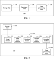
FIG. 1 is a schematic 1 of a structure of a data transmission circuit according to an embodiment of this application; -
FIG. 2 is a schematic 2 of a structure of a data transmission circuit according to an embodiment of this application; -
FIG. 3 is a schematic 3 of a structure of a data transmission circuit according to an embodiment of this application; -
FIG. 4 is a schematic 4 of a structure of a data transmission circuit according to an embodiment of this application; and -
FIG. 5 is a schematic flowchart of a data transmission method according to an embodiment of this application. - Reference numerals:
- 100-data transmission circuit; 110-storage chip; 120-data transit chip; 121-read module;
- 122-first cache module; 123-decoding module; 124-second cache module; 125-encoding module;
- 1251-encoding unit; 1252-editing unit; 130-data processing chip; 131-third cache module;
- 132-memory module; 140-display driver integrated circuit.
- The technical solutions in embodiments of this application are clearly described in the following with reference to accompanying drawings in embodiments of this application. Apparently, the described embodiments are some rather than all of embodiments of this application. All other embodiments obtained by a person of ordinary skill in the art based on embodiments of this application fall within the protection scope of this application.
- In the specification and the claims of this application, terms such as "first" and "second" are used to distinguish between similar objects rather than to describe a specific sequence or order. It should be understood that data used in this way is exchangeable in a proper case, so that embodiments of this application can be implemented in an order different from the order illustrated or described herein. The objects distinguished by "first", "second", and the like are usually of a same category, and a quantity of the objects is not limited. For example, there may be one or more first objects. In addition, in the specification and the claims, "and/or" indicates at least one of connected objects, and the character "/" usually indicates an "or" relationship between associated objects.
- With reference to the accompanying drawings, the following describes, in detail based on the specific embodiments and application scenarios thereof, a data transmission circuit, a data transmission method, and an electronic device that are provided in the embodiments of this application.
- An embodiment of this application provides a
data transmission circuit 100. As shown inFIG. 1 , thedata transmission circuit 100 includes astorage chip 110, adata transit chip 120, and adata processing chip 130. - The
storage chip 110, thedata transit chip 120, and thedata processing chip 130 are sequentially connected in series. - The
data transit chip 120 is configured to read a first data packet with a first preset quantity of bits from thestorage chip 110, process the first data packet into a plurality of second data packets each with a second preset quantity of bits, and send the second data packets to thedata processing chip 130. - A maximum quantity of bits of a data packet that the
data processing chip 130 is able to read at a time is a third preset quantity of bits, the second preset quantity of bits is less than or equal to the third preset quantity of bits, and the first preset quantity of bits is greater than the third preset quantity of bits. - In this embodiment of this application, the
storage chip 110 is configured to store data. The data may be, for example, a color curve parameter among screen display parameters of an electronic device. - In an embodiment of this application, the
storage chip 110 may be, for example, a flash. - In an embodiment of this application, the
data transit chip 120 may be a frame interpolation chip. In this embodiment of this application, thedata transit chip 120 in this embodiment of this application is implemented by using a frame interpolation chip, so that there is no need to develop a new chip. Based on this, hardware costs and design difficulty of thedata transmission circuit 100 provided in this embodiment of this application can be reduced. - In an embodiment of this application, the
data processing chip 130 may be a CPU. - In this embodiment of this application, the
data transit chip 120 reads the first data packet with the first preset quantity of bits from thestorage chip 110, and processes the first data packet into the plurality of second data packets each with the second preset quantity of bits. Because the second preset quantity of bits is less than or equal to the third preset quantity of bits and the third preset quantity of bits is the maximum quantity of bits of a data packet that thedata processing chip 130 is able to read at a time, thedata processing chip 130 may read the second data packets after thedata transit chip 120 sends the second data packets to thedata processing chip 130. Based on this, thedata processing chip 130 can indirectly read the first data packet by reading the plurality of consecutive second data packets each with the second preset quantity of bits. In other words, thedata transmission circuit 100 provided in this embodiment of this application can resolve a problem that thedata processing chip 130 cannot read the first data packet with the first preset quantity of bits. Based on this, in a case that thedata processing chip 130 is a CPU and thestorage chip 110 is a flash, the CPU can still indirectly read data in the flash although there is a limitation on a MIPI buffer. This resolves a problem that the CPU cannot read the data in the flash. - In addition, for the
data transmission circuit 100 provided based on this embodiment of this application, there is no need to improve a memory module in thedata processing chip 130 to enable the memory module to support the first data packet with the first preset quantity of bits. This lowers a requirement on thedata processing chip 130. - In an example, the first preset quantity of bits is 200 bits.
- It should be noted that, in a case that the second data packets include only valid data, the second preset quantity of bits is less than or equal to the third preset quantity of bits.
- In a case that the second data packets further include other data (for example, a verification code, a start character, and an end character) in addition to valid data, the second preset quantity of bits is less than the third preset quantity of bits, and a sum of the second preset quantity of bits and a quantity of bits corresponding to the other data is less than or equal to the third preset quantity of bits.
- In this embodiment of this application, the data transmission circuit is provided. The data transmission circuit includes the storage chip, the data transit chip, and the data processing chip, where the storage chip, the data transit chip, and the data processing chip are sequentially connected in series; the data transit chip is configured to read the first data packet with the first preset quantity of bits from the storage chip, process the first data packet into the plurality of second data packets each with the second preset quantity of bits, and send the second data packets to the data processing chip; and the maximum quantity of bits of a data packet that the data processing chip is able to read at a time is the third preset quantity of bits, the second preset quantity of bits is less than or equal to the third preset quantity of bits, and the first preset quantity of bits is greater than the third preset quantity of bits. The data transmission circuit provided in this embodiment of this application can resolve the problem that the data processing chip cannot read the first data packet with the first preset quantity of bits. Based on this, in the case that the data processing chip is a CPU and the storage chip is a flash, the CPU can still indirectly read the data in the flash although there is the limitation on the MIPI buffer. This resolves the problem that the CPU cannot read the data in the flash.
- In an embodiment of this application, as shown in
FIG. 2 , adata transit chip 120 includes aread module 121, afirst cache module 122, adecoding module 123, asecond cache module 124, and anencoding module 125. - A first end of the
read module 121 is connected to astorage chip 110. - A second end of the
read module 121, a first end of thefirst cache module 122, a second end of thefirst cache module 122, thedecoding module 123, thesecond cache module 124, and a first end of theencoding module 125 are sequentially connected in series. - A second end of the
encoding module 125 is connected to adata processing chip 130. - The
read module 121 reads a first data packet with a first preset quantity of bits from thestorage chip 110 and saves the first data packet in thefirst cache module 122, thedecoding module 123 decodes the first data packet cached in thefirst cache module 122 and saves decoded data in thesecond cache module 124, and theencoding module 125 encodes, into a plurality of second data packets each with a second preset quantity of bits, data that is read from thesecond cache module 124. - In this embodiment of this application, a manner in which the
read module 121 reads the first data packet with the first preset quantity of bits from thestorage chip 110 and saves the first data packet in thefirst cache module 122 may be as follows: Theread module 121 determines a data reading instruction, where the data reading instruction includes an address of to-be-read data in thestorage chip 110; theread module 121 reads, according to the reading instruction, data from an address in thestorage chip 110 that is the same as the address included in the reading instruction; the data is denoted as the first data packet, and a size of the data is the first preset quantity of bits; and theread module 121 caches the first data packet in thefirst cache module 122. - The manner in which the
read module 121 reads the first data packet with the first preset quantity of bits from thestorage chip 110 and saves the first data packet in thefirst cache module 122 may alternatively be as follows: Theread module 121 is connected to thestorage chip 110 by a display driver integratedcircuit 140; theread module 121 sends a data reading instruction like the foregoing one to the display driver integratedcircuit 140; the display driver integratedcircuit 140 reads, according to the data reading instruction, data from an address in thestorage chip 110 that is the same as an address included in the reading instruction; the data is denoted as the first data packet, and a size of the data is the first preset quantity of bits; and the display driver integratedcircuit 140 caches the first data packet in thefirst cache module 122. It should be noted that in this manner, thefirst cache module 122 needs to notify theread module 121 of related information that is stored. - The
first cache module 122 is a cache module with a high data transmission rate, so as to be suitable for fast reading performed by theread module 121. - In this embodiment of this application, the
decoding module 123 decodes the first data packet cached in thefirst cache module 122, so that the first data packet is decoded into a format that can be recognized by thesecond cache module 124; and saves decoded data in the second cache module. A size of each data packet stored in thesecond cache module 124 is usually 1 bit. - In an embodiment of this application, the
second cache module 124 is a module with a high storage capacity. For example, thesecond cache module 124 may be, for example, a frame buffer. - The
encoding module 125 reads the data from thesecond cache module 124, and processes the data into the second data packets each with the second preset quantity of bits. The processing at least includes encoding the read data into a format that can be recognized by thedata processing chip 130. Further, the processing may further include adding start characters to packet headers, and adding end characters to packet trailers or adding verification codes and end characters to packet trailers of data packets encoded in the format that can be recognized by thedata processing chip 130, after the read data is encoded into the format that can be recognized by thedata processing chip 130. - In this embodiment of this application, a specific structure of the
data transit chip 120 is provided. The structure is simple and easy to implement. This can reduce the hardware costs of the data transmission circuit provided in this embodiment of this application. - It can be understood that based on the foregoing manner in which the
read module 121 sends the data reading instruction to the display driver integratedcircuit 140 to read the first data packet, as shown inFIG. 3 , thedata transmission circuit 100 provided in this embodiment of this application further includes a display driver integratedcircuit 140. - The display driver integrated
circuit 140 includes a first end, a second end, and a third end, and afirst cache module 122 further includes a third end. - The first end of the display driver integrated
circuit 140 is connected to astorage chip 110, the second end of the display driver integratedcircuit 140 is connected to a first end of aread module 121, and the third end of the display driver integratedcircuit 140 is connected to the third end of thefirst cache module 122. - Based on the foregoing content, that the
read module 121 reads a first data packet with a first preset quantity of bits from thestorage chip 110 and saves the first data packet in thefirst cache module 122 includes: - the
read module 121 sends a data reading instruction to the display driver integratedcircuit 140; and - the display driver integrated
circuit 140 reads the first data packet with the first preset quantity of bits from thestorage chip 110 according to the data reading instruction, and saves the first data packet in thefirst cache module 122. - In this embodiment of this application, the
read module 121 reads the first data packet by sending the data reading instruction to the display driver integratedcircuit 140. For an electronic device that integrates thestorage chip 110 and the display driver integratedcircuit 140, there is no need to improve hardware. This reduces the hardware costs of thedata transmission circuit 100 provided in this embodiment of this application. - In an embodiment of this application, as shown in
FIG. 4 , anencoding module 125 includes anencoding unit 1251 and anediting unit 1252. - The
encoding unit 1251 includes a first end and a second end, and theediting unit 1252 includes a first end and a second end. - The first end of the
encoding unit 1251 is connected to asecond cache module 124, and the second end of theencoding unit 1251 is connected to the first end of theediting unit 1252. - The second end of the
editing unit 1252 is connected to adata processing chip 130. - In this embodiment of this application, the
encoding unit 1251 encodes, into a plurality of second data packets, data that is read from the second cache module. - In an embodiment of this application, for any one of the second data packets, the
editing unit 1252 adds a start character to a packet header of the second data packet and adds an end character to a packet trailer of the second data packet, to update the second data packet; and sends the updated second data packet to thedata processing chip 130. - In this embodiment of this application, by adding a start character to a packet header and adding an end character to a packet trailer of a second data packet, the
editing unit 1252 may enable thedata processing chip 130 to obtain an accurate second data packet based on the start character and the end character. - In an embodiment of this application, the
editing unit 1252 generates a first verification code for the any one of the second data packets based on the second data packet. - For the any one of the second data packets, a start character is added to a packet header of the second data packet, and the first verification code and an end character are sequentially added to a packet trailer of the second data packet, to update the second data packet. The updated second data packet is sent to the
data processing chip 130. - In this embodiment of this application, the
editing unit 1252 may generate a first verification code based on a second data packet by using a first verification algorithm, for example, a CRC verification algorithm. A quantity of digits of the first verification code is usually fixed. It should be noted that thedata processing chip 130 includes the same first verification algorithm. - In this embodiment of this application, after obtaining a data packet sent by the
editing unit 1252, thedata processing chip 130 identifies a start character, a second data packet, a first verification code, and an end character. Further, thedata processing chip 130 determines a verification code based on the second data packet and the same first verification algorithm, and denotes the verification code as a first check verification code. Still further, thedata processing chip 130 determines whether the first check verification code is the same as the first verification code according to the first check verification code. In a case that the first check verification code is the same as the first verification code, the second data packet is determined to be correct. In a case that the first check verification code is different from the first verification code, the second data packet is determined to be incorrect. In a case that the second data packet is determined to be incorrect, adata transit chip 120 is notified to retransmit the second data packet. Based on this, thedata processing chip 130 may obtain a correct second data packet. - In an embodiment of this application, as shown in
FIG. 4 , adata processing chip 130 includes athird cache module 131 and amemory module 132. - The
third cache module 131 includes a first end and a second end, the first end of thethird cache module 131 is connected to anencoding module 125, and the second end of thethird cache module 131 is connected to thememory module 132. - In this embodiment of this application, after obtaining second data packets, the
data processing chip 130 saves the second data packets in thethird cache module 131, and then thethird cache module 131 dumps the second data packets to thememory module 132, so that the second data packets are stably stored in thedata processing chip 130 for use by a display screen or another component of an electronic device. - In an embodiment of this application, the first data packet includes valid data and a second verification code. That the
read module 121 reads the first data packet with the first preset quantity of bits from thestorage chip 110 and saves the first data packet in the first cache module specifically includes: - based on the valid data and the second verification code in the first data packet, determining whether the first data packet is correct; and
- in a case that the first data packet is determined to be correct, saving the first data packet in the
first cache module 122. - In this embodiment of this application, based on the valid data in the first data packet and a second verification algorithm, for example, a CRC verification algorithm, a verification code corresponding to the valid data in the first data packet is determined and is denoted as a second check verification code. It should be noted that the
storage chip 110 includes the same second verification algorithm. Thestorage chip 110 generates, based on the same second verification algorithm, the second verification code for data that is read, so as to add the second verification code to a valid data packet to form the first data packet. - The
read module 121 determines whether the second verification code is the same as the second check verification code. In a case that the second verification code is the same as the second check verification code, the first data packet is determined to be correct. In this case, the first data packet is saved in thefirst cache module 122. In a case that the second verification code is different from the second check verification code, the first data packet with the first preset quantity of bits is read from thestorage chip 110 again. - In an embodiment of this application, an electronic device is provided. The electronic device includes the
data transmission circuit 100 according to any one of the foregoing embodiments. - In an embodiment of this application, the electronic device may be, for example, a mobile phone, a tablet computer, a notebook computer, a palmtop computer, a vehicle-mounted electronic device, a mobile Internet device (Mobile Internet Device, MID), an augmented reality (augmented reality, AR) or a virtual reality (virtual reality, VR) device, a robot, a wearable device, an ultra-mobile personal computer (ultra-mobile personal computer, UMPC), a netbook, a personal digital assistant (personal digital assistant, PDA), or the like, or may be a server, a network attached storage (Network Attached Storage, NAS), a personal computer (personal computer, PC), a television (television, TV), a teller machine, a self-service machine, or the like. This is not specifically limited in this embodiment of this application.
- An embodiment of this application further provides a data transmission method. The method is applied to the
data transmission circuit 100 according to any one of the foregoing embodiments, and as shown inFIG. 5 , includes the following S5100 to S5300. - S5100: A
data transit chip 120 reads a first data packet with a first preset quantity of bits from astorage chip 110. - S5200: The
data transit chip 120 processes the first data packet into a plurality of second data packets each with a second preset quantity of bits. - S5300: The
data transit chip 120 sends the second data packets to adata processing chip 130. - A maximum quantity of bits of a data packet that the
data processing chip 130 is able to read at a time is a third preset quantity of bits, the second preset quantity of bits is less than or equal to the third preset quantity of bits, and the first preset quantity of bits is greater than the third preset quantity of bits. - In this embodiment of this application, the data transmission method is provided. The method is applied to the data transmission circuit according to the any one of the foregoing embodiments, and includes: reading, by the data transit chip, the first data packet with the first preset quantity of bits from the storage chip; processing the first data packet into the plurality of second data packets each with the second preset quantity of bits; and sending, by the data transit chip, the second data packets to the data processing chip. The first preset quantity of bits is greater than the second preset quantity of bits. The maximum quantity of bits of a data packet that the data processing chip is able to read at a time is the third preset quantity of bits. The second preset quantity of bits is less than or equal to the third preset quantity of bits. The data transmission method provided in this embodiment of this application can resolve a problem that the data processing chip cannot read the first data packet with the first preset quantity of bits. Based on this, in a case that the
data processing chip 130 is a CPU and the storage chip is a flash, the CPU can still indirectly read data in the flash although there is a limitation on a MIPI buffer. This resolves a problem that the CPU cannot read the data in the flash. - In an embodiment of this application, the
data transit chip 120 includes aread module 121, afirst cache module 122, adecoding module 123, asecond cache module 124, and anencoding module 125. Based on this, a specific implementation of the foregoing S5100 may be the following S5110. - S5110: The
read module 121 reads the first data packet with the first preset quantity of bits from thestorage chip 110, and saves the first data packet in the first cache module. - A specific implementation of the foregoing S5200 may be the following S5210 and S5220.
- S5210: The decoding module decodes the first data packet cached in the first cache module, and saves decoded data in the second cache module.
- S5220: The encoding module processes, into the plurality of second data packets each with the second preset quantity of bits, data that is read from the second cache module.
- In an embodiment of this application, a specific implementation of the foregoing S5110 may be the following S5111 and S5112.
- S5111: The
read module 121 sends a data reading instruction to a display driver integratedcircuit 140. - S5112: The display driver integrated
circuit 140 reads the first data packet with the first preset quantity of bits from thestorage chip 110 according to the data reading instruction, and saves the first data packet in thefirst cache module 122. - In an embodiment of this application, the
encoding module 125 includes anencoding unit 1251 and anediting unit 1252. Based on this, a specific implementation of the foregoing S5220 may be the following S5221 and S5222. - S5221: The
encoding unit 1251 encodes, into the plurality of second data packets each with the second preset quantity of bits, the data that is read from the second cache module. - S5222: The
editing unit 1252 generates a first verification code for any one of the second data packets based on the second data packet. - For the any one of the second data packets, a start character is added to a packet header of the second data packet and the first verification code and an end character are sequentially added to a packet trailer of the second data packet, to update the second data packet. The updated second data packet is sent to the
data processing chip 130. - It should be noted that for implementation of the steps in the foregoing method embodiments, reference may be made to the specific related implementation of the foregoing
data transmission circuit 100. Details are not described herein again. - It should be noted that the term "include", "comprise", or any other variation thereof in this specification is intended to cover a non-exclusive inclusion, so that a process, a method, an article, or an apparatus that includes a list of elements not only includes those elements but also includes other elements that are not expressly listed, or further includes elements inherent to the process, method, article, or apparatus. In absence of more constraints, an element preceded by "includes a ..." does not preclude existence of other identical elements in the process, method, article, or apparatus that includes the element. In addition, it should be noted that in the scope of the method and apparatus in embodiments of this application, an order in which functions are performed is not limited to the shown or discussed order, and may further include an order in which the functions are substantially performed at the same time or a reverse order, depending on the related functions. For example, the described method may be performed in an order different from the described order, and steps may be added, omitted, or combined. In addition, features described with reference to some examples may be combined in other examples.
- According to the descriptions of the foregoing implementations, a person skilled in the art can clearly understand that the method in the foregoing embodiments may be implemented by software and a necessary universal hardware platform or by hardware only. In most cases, the former is a better implementation. Based on such an understanding, the technical solutions of this application essentially, or the part contributing to the prior art, may be presented in the form of a computer software product. The computer software product is stored in a storage medium (for example, a ROM/RAM, a magnetic disk, or an optical disc), and includes several instructions to enable a terminal (which may be a mobile phone, a computer, a server, a network device, or the like) to perform the method described in embodiments of this application.
- Embodiments of this application are described above with reference to the accompanying drawings. However, this application is not limited to the foregoing specific embodiments. The foregoing specific embodiments are only illustrative rather than restrictive. Inspired by this application, a person of ordinary skill in the art can still derive a plurality of variations without departing from the essence of this application and the protection scope of the claims. All these variations shall fall within the protection of this application.
Claims (10)
- A data transmission circuit, comprising a storage chip, a data transit chip, and a data processing chip, whereinthe storage chip, the data transit chip, and the data processing chip are sequentially connected in series;the data transit chip is configured to read a first data packet with a first preset quantity of bits from the storage chip, process the first data packet into a plurality of second data packets each with a second preset quantity of bits, and send the second data packets to the data processing chip; anda maximum quantity of bits of a data packet that the data processing chip is able to read at a time is a third preset quantity of bits, the second preset quantity of bits is less than or equal to the third preset quantity of bits, and the first preset quantity of bits is greater than the third preset quantity of bits.
- The data transmission circuit according to claim 1, wherein the data transit chip comprises a read module, a first cache module, a decoding module, a second cache module, and an encoding module, whereina first end of the read module is connected to the storage chip;a second end of the read module, a first end of the first cache module, a second end of the first cache module, the decoding module, the second cache module, and a first end of the encoding module are sequentially connected in series; anda second end of the encoding module is connected to the data processing chip, wherein the read module reads the first data packet with the first preset quantity of bits from the storage chip and saves the first data packet in the first cache module, the decoding module decodes the first data packet cached in the first cache module and saves decoded data in the second cache module, and the encoding module processes, into the plurality of second data packets each with the second preset quantity of bits, data that is read from the second cache module.
- The data transmission circuit according to claim 2, further comprising a display driver integrated circuit, whereinthe display driver integrated circuit comprises a first end, a second end, and a third end, and the first cache module further comprises a third end; andthe first end of the display driver integrated circuit is connected to the storage chip, the second end of the display driver integrated circuit is connected to the first end of the read module, and the third end of the display driver integrated circuit is connected to the third end of the first cache module.
- The data transmission circuit according to claim 2, wherein the encoding module comprises an encoding unit and an editing unit, whereinthe encoding module comprises a first end and a second end, and the editing unit comprises a first end and a second end;the first end of the encoding unit is connected to the second cache module, and the second end of the encoding unit is connected to the first end of the editing unit; andthe second end of the editing unit is connected to the data processing chip.
- The data transmission circuit according to claim 2, wherein the data processing chip comprises a third cache module and a memory module, wherein
the third cache module comprises a first end and a second end, the first end of the third cache module is connected to the encoding module, and the second end of the third cache module is connected to the memory module. - A data transmission method, applied to the data transmission circuit according to any one of claims 1 to 5, wherein the method comprises:reading, by a data transit chip, a first data packet with a first preset quantity of bits from a storage chip;processing, by the data transit chip, the first data packet into a plurality of second data packets each with a second preset quantity of bits; andsending, by the data transit chip, the second data packets to a data processing chip, whereina maximum quantity of bits of a data packet that the data processing chip is able to read at a time is a third preset quantity of bits, the second preset quantity of bits is less than or equal to the third preset quantity of bits, and the first preset quantity of bits is greater than the third preset quantity of bits.
- The method according to claim 6, wherein the data transit chip comprises a read module, a first cache module, a decoding module, a second cache module, and an encoding module;
the reading, by a data transit chip, a first data packet with a first preset quantity of bits from a storage chip comprises:reading, by the read module, the first data packet with the first preset quantity of bits from the storage chip, and saving the first data packet in the first cache module; andthe processing, by the data transit chip, the first data packet into a plurality of second data packets each with a second preset quantity of bits comprises:decoding, by the decoding module, the first data packet cached in the first cache module, and saving decoded data in the second cache module; andprocessing, by the encoding module into the plurality of second data packets each with the second preset quantity of bits, data that is read from the second cache module. - The method according to claim 7, wherein the reading, by the read module, the first data packet with the first preset quantity of bits from the storage chip, and saving the first data packet in the first cache module comprises:sending, by the read module, a data reading instruction to a display driver integrated circuit; andreading, by the display driver integrated circuit, the first data packet with the first preset quantity of bits from the storage chip according to the data reading instruction, and saving the first data packet in the first cache module.
- The method according to claim 7, wherein the encoding module comprises an encoding unit and an editing unit; and
the encoding, by the encoding module into the plurality of second data packets each with the second preset quantity of bits, data that is read from the second cache module comprises:encoding, by the encoding unit into the plurality of second data packets each with the second preset quantity of bits, the data that is read from the second cache module; andgenerating, by the editing unit, a first verification code for any one of the second data packets based on the second data packet; andfor the any one of the second data packets, adding a start character to a packet header of the second data packet and sequentially adding the first verification code and an end character to a packet trailer of the second data packet, to update the second data packet, and sending the updated second data packet to the data processing chip. - An electronic device, wherein the electronic device comprises the data transmission circuit according to any one of claims 1 to 5.
Applications Claiming Priority (2)
| Application Number | Priority Date | Filing Date | Title |
|---|---|---|---|
| CN202210619178.9A CN115048049A (en) | 2022-05-31 | 2022-05-31 | Data transmission circuit, data transmission method and electronic equipment |
| PCT/CN2023/095981 WO2023231858A1 (en) | 2022-05-31 | 2023-05-24 | Data transmission circuit, data transmission method, and electronic device |
Publications (2)
| Publication Number | Publication Date |
|---|---|
| EP4535150A1 true EP4535150A1 (en) | 2025-04-09 |
| EP4535150A4 EP4535150A4 (en) | 2025-10-08 |
Family
ID=83158927
Family Applications (1)
| Application Number | Title | Priority Date | Filing Date |
|---|---|---|---|
| EP23815042.9A Pending EP4535150A4 (en) | 2022-05-31 | 2023-05-24 | DATA TRANSMISSION CIRCUIT, DATA TRANSMISSION METHOD AND ELECTRONIC DEVICE |
Country Status (4)
| Country | Link |
|---|---|
| US (1) | US20250068353A1 (en) |
| EP (1) | EP4535150A4 (en) |
| CN (1) | CN115048049A (en) |
| WO (1) | WO2023231858A1 (en) |
Families Citing this family (1)
| Publication number | Priority date | Publication date | Assignee | Title |
|---|---|---|---|---|
| CN115048049A (en) * | 2022-05-31 | 2022-09-13 | 维沃移动通信有限公司 | Data transmission circuit, data transmission method and electronic equipment |
Family Cites Families (17)
| Publication number | Priority date | Publication date | Assignee | Title |
|---|---|---|---|---|
| JP4600511B2 (en) * | 2008-04-23 | 2010-12-15 | 沖電気工業株式会社 | Codec conversion device, gateway device, and codec conversion method |
| US8315152B2 (en) * | 2008-06-06 | 2012-11-20 | Maxim Integrated Products, Inc. | System and method for applying multi-tone OFDM based communications within a prescribed frequency range |
| CN101645053B (en) * | 2009-06-29 | 2011-01-05 | 福建星网锐捷网络有限公司 | Method for improving data transmission efficiency and device thereof |
| US20110019668A1 (en) * | 2009-07-24 | 2011-01-27 | Wael William Diab | Method And System For Packet Preemption Via Packet Rescheduling |
| US10446071B2 (en) * | 2016-03-31 | 2019-10-15 | Samsung Electronics Co., Ltd. | Device and method of using slice update map |
| CN106294234B (en) * | 2016-08-01 | 2018-09-21 | 深圳云天励飞技术有限公司 | A kind of data transmission method and device |
| US10282109B1 (en) * | 2016-09-15 | 2019-05-07 | Altera Corporation | Memory interface circuitry with distributed data reordering capabilities |
| US11436968B2 (en) * | 2017-06-16 | 2022-09-06 | Synaptics Incorporated | Display driver, image processing circuitry, and method |
| CN111222306A (en) * | 2020-01-06 | 2020-06-02 | 广州虎牙科技有限公司 | Data processing method and device, electronic equipment and storage medium |
| US11327687B2 (en) * | 2020-03-18 | 2022-05-10 | Arm Limited | Encoding data arrays |
| KR102708771B1 (en) * | 2020-05-25 | 2024-09-20 | 삼성전자주식회사 | A display drive ic and a display device including the same |
| US11418455B2 (en) * | 2020-08-31 | 2022-08-16 | Micron Technology, Inc. | Transparent packet splitting and recombining |
| CN112256626B (en) * | 2020-10-16 | 2024-12-20 | 北京声智科技有限公司 | Data processing method, device, electronic device and computer readable storage medium |
| CN113489575A (en) * | 2021-06-25 | 2021-10-08 | 阿波罗智联(北京)科技有限公司 | Data transmission method and device and electronic equipment |
| CN114063932A (en) * | 2021-11-26 | 2022-02-18 | 新华三技术有限公司合肥分公司 | Data storage method, data reading method and electronic equipment |
| US11645222B1 (en) * | 2022-01-11 | 2023-05-09 | United States Of America As Represented By The Secretary Of The Air Force | Real time generation of differential serial bus traffic |
| CN115048049A (en) * | 2022-05-31 | 2022-09-13 | 维沃移动通信有限公司 | Data transmission circuit, data transmission method and electronic equipment |
-
2022
- 2022-05-31 CN CN202210619178.9A patent/CN115048049A/en active Pending
-
2023
- 2023-05-24 EP EP23815042.9A patent/EP4535150A4/en active Pending
- 2023-05-24 WO PCT/CN2023/095981 patent/WO2023231858A1/en not_active Ceased
-
2024
- 2024-11-12 US US18/944,310 patent/US20250068353A1/en active Pending
Also Published As
| Publication number | Publication date |
|---|---|
| CN115048049A (en) | 2022-09-13 |
| US20250068353A1 (en) | 2025-02-27 |
| WO2023231858A1 (en) | 2023-12-07 |
| EP4535150A4 (en) | 2025-10-08 |
Similar Documents
| Publication | Publication Date | Title |
|---|---|---|
| US10825130B2 (en) | Method and apparatus for displaying picture content in application, and storage medium | |
| CN111506452B (en) | Data storage protection method, device, computer equipment and storage medium | |
| JP5160187B2 (en) | Image output apparatus and method for portable terminal | |
| US20250068353A1 (en) | Data transmission circuit, data transmission method, and electronic device | |
| WO2023103336A1 (en) | Video data transmission method, video data decoding method, and related apparatuses | |
| EP2153634A1 (en) | Methods, systems and computer program products for modifying an electronic text message with warped images | |
| US12143609B2 (en) | Video data transmission method, video data decoding method, and related apparatuses | |
| JP2005092203A (en) | YUV display buffer | |
| EP2482230B1 (en) | Apparatus and method for decoding matrix code symbol | |
| EP4727128A1 (en) | Gain map encoding method and apparatus, gain map decoding method and apparatus, device, and medium | |
| US20260079817A1 (en) | Media data processing method and apparatus, electronic device, and readable storage medium | |
| KR20090064486A (en) | System and method for providing Internet web page in mobile communication network | |
| CN117076799B (en) | Caching methods, devices, and storage media for front-end resources | |
| US7861007B2 (en) | Method and apparatus for multimedia display in a mobile device | |
| US8768387B2 (en) | Message transmitting apparatus and method in mobile communication terminal | |
| US7058308B2 (en) | Method for communicating multimedia data between electronic devices by means of IR ray | |
| CN115665481A (en) | Video processing apparatus, method, device, and storage medium | |
| US6035068A (en) | Method and apparatus for processing compressed data and non-compressed data | |
| US7751637B2 (en) | Method and apparatus for synthesizing data | |
| KR100392819B1 (en) | Method and apparatus for generating and storing Font Rom | |
| CN115309349B (en) | Deep learning sparse data storage method, computer device and storage medium | |
| US20030215148A1 (en) | Apparatus and method for compressing/decompressing images in a mobile communication terminal | |
| CN121568077A (en) | Bluetooth communication method and device and electronic equipment | |
| CN117272926A (en) | Dynamic font generation method, generation device and computer-readable storage medium | |
| JP3190855B2 (en) | Decompression method of compressed data |
Legal Events
| Date | Code | Title | Description |
|---|---|---|---|
| STAA | Information on the status of an ep patent application or granted ep patent |
Free format text: STATUS: THE INTERNATIONAL PUBLICATION HAS BEEN MADE |
|
| PUAI | Public reference made under article 153(3) epc to a published international application that has entered the european phase |
Free format text: ORIGINAL CODE: 0009012 |
|
| STAA | Information on the status of an ep patent application or granted ep patent |
Free format text: STATUS: REQUEST FOR EXAMINATION WAS MADE |
|
| 17P | Request for examination filed |
Effective date: 20240910 |
|
| AK | Designated contracting states |
Kind code of ref document: A1 Designated state(s): AL AT BE BG CH CY CZ DE DK EE ES FI FR GB GR HR HU IE IS IT LI LT LU LV MC ME MK MT NL NO PL PT RO RS SE SI SK SM TR |
|
| DAV | Request for validation of the european patent (deleted) | ||
| DAX | Request for extension of the european patent (deleted) | ||
| A4 | Supplementary search report drawn up and despatched |
Effective date: 20250909 |
|
| RIC1 | Information provided on ipc code assigned before grant |
Ipc: G06F 3/06 20060101AFI20250903BHEP Ipc: G06F 11/10 20060101ALI20250903BHEP Ipc: G06F 13/16 20060101ALI20250903BHEP Ipc: G06F 13/40 20060101ALI20250903BHEP |