EP4531518A1 - Semiconductor device - Google Patents
Semiconductor device Download PDFInfo
- Publication number
- EP4531518A1 EP4531518A1 EP24200986.8A EP24200986A EP4531518A1 EP 4531518 A1 EP4531518 A1 EP 4531518A1 EP 24200986 A EP24200986 A EP 24200986A EP 4531518 A1 EP4531518 A1 EP 4531518A1
- Authority
- EP
- European Patent Office
- Prior art keywords
- layer
- semiconductor layer
- insulating layer
- oxide semiconductor
- electrode
- Prior art date
- Legal status (The legal status is an assumption and is not a legal conclusion. Google has not performed a legal analysis and makes no representation as to the accuracy of the status listed.)
- Granted
Links
Images








Classifications
-
- H—ELECTRICITY
- H10—SEMICONDUCTOR DEVICES; ELECTRIC SOLID-STATE DEVICES NOT OTHERWISE PROVIDED FOR
- H10D—INORGANIC ELECTRIC SEMICONDUCTOR DEVICES
- H10D30/00—Field-effect transistors [FET]
- H10D30/60—Insulated-gate field-effect transistors [IGFET]
- H10D30/67—Thin-film transistors [TFT]
- H10D30/6729—Thin-film transistors [TFT] characterised by the electrodes
- H10D30/673—Thin-film transistors [TFT] characterised by the electrodes characterised by the shapes, relative sizes or dispositions of the gate electrodes
- H10D30/6733—Multi-gate TFTs
- H10D30/6734—Multi-gate TFTs having gate electrodes arranged on both top and bottom sides of the channel, e.g. dual-gate TFTs
-
- H—ELECTRICITY
- H10—SEMICONDUCTOR DEVICES; ELECTRIC SOLID-STATE DEVICES NOT OTHERWISE PROVIDED FOR
- H10D—INORGANIC ELECTRIC SEMICONDUCTOR DEVICES
- H10D86/00—Integrated devices formed in or on insulating or conducting substrates, e.g. formed in silicon-on-insulator [SOI] substrates or on stainless steel or glass substrates
- H10D86/40—Integrated devices formed in or on insulating or conducting substrates, e.g. formed in silicon-on-insulator [SOI] substrates or on stainless steel or glass substrates characterised by multiple TFTs
- H10D86/471—Integrated devices formed in or on insulating or conducting substrates, e.g. formed in silicon-on-insulator [SOI] substrates or on stainless steel or glass substrates characterised by multiple TFTs having different architectures, e.g. having both top-gate and bottom-gate TFTs
-
- H—ELECTRICITY
- H10—SEMICONDUCTOR DEVICES; ELECTRIC SOLID-STATE DEVICES NOT OTHERWISE PROVIDED FOR
- H10D—INORGANIC ELECTRIC SEMICONDUCTOR DEVICES
- H10D30/00—Field-effect transistors [FET]
- H10D30/60—Insulated-gate field-effect transistors [IGFET]
- H10D30/67—Thin-film transistors [TFT]
- H10D30/6729—Thin-film transistors [TFT] characterised by the electrodes
- H10D30/673—Thin-film transistors [TFT] characterised by the electrodes characterised by the shapes, relative sizes or dispositions of the gate electrodes
- H10D30/6731—Top-gate only TFTs
-
- H—ELECTRICITY
- H10—SEMICONDUCTOR DEVICES; ELECTRIC SOLID-STATE DEVICES NOT OTHERWISE PROVIDED FOR
- H10D—INORGANIC ELECTRIC SEMICONDUCTOR DEVICES
- H10D30/00—Field-effect transistors [FET]
- H10D30/60—Insulated-gate field-effect transistors [IGFET]
- H10D30/67—Thin-film transistors [TFT]
- H10D30/6729—Thin-film transistors [TFT] characterised by the electrodes
- H10D30/6737—Thin-film transistors [TFT] characterised by the electrodes characterised by the electrode materials
-
- H—ELECTRICITY
- H10—SEMICONDUCTOR DEVICES; ELECTRIC SOLID-STATE DEVICES NOT OTHERWISE PROVIDED FOR
- H10D—INORGANIC ELECTRIC SEMICONDUCTOR DEVICES
- H10D30/00—Field-effect transistors [FET]
- H10D30/60—Insulated-gate field-effect transistors [IGFET]
- H10D30/67—Thin-film transistors [TFT]
- H10D30/674—Thin-film transistors [TFT] characterised by the active materials
- H10D30/6741—Group IV materials, e.g. germanium or silicon carbide
- H10D30/6743—Silicon
- H10D30/6745—Polycrystalline or microcrystalline silicon
-
- H—ELECTRICITY
- H10—SEMICONDUCTOR DEVICES; ELECTRIC SOLID-STATE DEVICES NOT OTHERWISE PROVIDED FOR
- H10D—INORGANIC ELECTRIC SEMICONDUCTOR DEVICES
- H10D30/00—Field-effect transistors [FET]
- H10D30/60—Insulated-gate field-effect transistors [IGFET]
- H10D30/67—Thin-film transistors [TFT]
- H10D30/674—Thin-film transistors [TFT] characterised by the active materials
- H10D30/6755—Oxide semiconductors, e.g. zinc oxide, copper aluminium oxide or cadmium stannate
-
- H—ELECTRICITY
- H10—SEMICONDUCTOR DEVICES; ELECTRIC SOLID-STATE DEVICES NOT OTHERWISE PROVIDED FOR
- H10D—INORGANIC ELECTRIC SEMICONDUCTOR DEVICES
- H10D86/00—Integrated devices formed in or on insulating or conducting substrates, e.g. formed in silicon-on-insulator [SOI] substrates or on stainless steel or glass substrates
- H10D86/01—Manufacture or treatment
- H10D86/021—Manufacture or treatment of multiple TFTs
- H10D86/0221—Manufacture or treatment of multiple TFTs comprising manufacture, treatment or patterning of TFT semiconductor bodies
-
- H—ELECTRICITY
- H10—SEMICONDUCTOR DEVICES; ELECTRIC SOLID-STATE DEVICES NOT OTHERWISE PROVIDED FOR
- H10D—INORGANIC ELECTRIC SEMICONDUCTOR DEVICES
- H10D86/00—Integrated devices formed in or on insulating or conducting substrates, e.g. formed in silicon-on-insulator [SOI] substrates or on stainless steel or glass substrates
- H10D86/40—Integrated devices formed in or on insulating or conducting substrates, e.g. formed in silicon-on-insulator [SOI] substrates or on stainless steel or glass substrates characterised by multiple TFTs
- H10D86/421—Integrated devices formed in or on insulating or conducting substrates, e.g. formed in silicon-on-insulator [SOI] substrates or on stainless steel or glass substrates characterised by multiple TFTs having a particular composition, shape or crystalline structure of the active layer
- H10D86/423—Integrated devices formed in or on insulating or conducting substrates, e.g. formed in silicon-on-insulator [SOI] substrates or on stainless steel or glass substrates characterised by multiple TFTs having a particular composition, shape or crystalline structure of the active layer comprising semiconductor materials not belonging to the Group IV, e.g. InGaZnO
-
- H—ELECTRICITY
- H10—SEMICONDUCTOR DEVICES; ELECTRIC SOLID-STATE DEVICES NOT OTHERWISE PROVIDED FOR
- H10D—INORGANIC ELECTRIC SEMICONDUCTOR DEVICES
- H10D86/00—Integrated devices formed in or on insulating or conducting substrates, e.g. formed in silicon-on-insulator [SOI] substrates or on stainless steel or glass substrates
- H10D86/40—Integrated devices formed in or on insulating or conducting substrates, e.g. formed in silicon-on-insulator [SOI] substrates or on stainless steel or glass substrates characterised by multiple TFTs
- H10D86/421—Integrated devices formed in or on insulating or conducting substrates, e.g. formed in silicon-on-insulator [SOI] substrates or on stainless steel or glass substrates characterised by multiple TFTs having a particular composition, shape or crystalline structure of the active layer
- H10D86/425—Integrated devices formed in or on insulating or conducting substrates, e.g. formed in silicon-on-insulator [SOI] substrates or on stainless steel or glass substrates characterised by multiple TFTs having a particular composition, shape or crystalline structure of the active layer having different crystal properties in different TFTs or within an individual TFT
-
- H—ELECTRICITY
- H10—SEMICONDUCTOR DEVICES; ELECTRIC SOLID-STATE DEVICES NOT OTHERWISE PROVIDED FOR
- H10D—INORGANIC ELECTRIC SEMICONDUCTOR DEVICES
- H10D86/00—Integrated devices formed in or on insulating or conducting substrates, e.g. formed in silicon-on-insulator [SOI] substrates or on stainless steel or glass substrates
- H10D86/40—Integrated devices formed in or on insulating or conducting substrates, e.g. formed in silicon-on-insulator [SOI] substrates or on stainless steel or glass substrates characterised by multiple TFTs
- H10D86/60—Integrated devices formed in or on insulating or conducting substrates, e.g. formed in silicon-on-insulator [SOI] substrates or on stainless steel or glass substrates characterised by multiple TFTs wherein the TFTs are in active matrices
-
- H—ELECTRICITY
- H10—SEMICONDUCTOR DEVICES; ELECTRIC SOLID-STATE DEVICES NOT OTHERWISE PROVIDED FOR
- H10K—ORGANIC ELECTRIC SOLID-STATE DEVICES
- H10K59/00—Integrated devices, or assemblies of multiple devices, comprising at least one organic light-emitting element covered by group H10K50/00
- H10K59/10—OLED displays
- H10K59/12—Active-matrix OLED [AMOLED] displays
- H10K59/121—Active-matrix OLED [AMOLED] displays characterised by the geometry or disposition of pixel elements
- H10K59/1213—Active-matrix OLED [AMOLED] displays characterised by the geometry or disposition of pixel elements the pixel elements being TFTs
Definitions
- An embodiment of the present invention relates to a semiconductor device.
- a semiconductor device in which transistors made of different semiconductor materials are formed on the same substrate as a semiconductor layer.
- transistors made of different semiconductor materials are formed on the same substrate as a semiconductor layer.
- a transistor using silicon is used as a transistor requiring high-speed operation
- a transistor using an oxide semiconductor is used as a transistor requiring a switching operation, so that transistors having different characteristics depending on a required function can be formed on the same substrate.
- Patent Literature 1 discloses a display device in which a transistor in which silicon is used for a driving circuit is formed on the same substrate, and a transistor in which an oxide semiconductor is used for a display region is formed.
- Patent Literature 1 Japanese laid-open patent publication No. 2018-128693
- An object of an embodiment of the present invention is to provide a highly productive semiconductor device that achieves good characteristics for each transistor having different characteristics.
- a semiconductor device includes: a first semiconductor layer; a first gate electrode facing the first semiconductor layer; a first gate insulating layer between the first semiconductor layer and the first gate electrode; a first insulating layer arranged above the first gate electrode; a first electrode arranged in a region overlapping the first semiconductor layer in a plan view, and electrically connected to the first semiconductor layer; a second semiconductor layer arranged above the first insulating layer and made of a different material from the first semiconductor layer; a second gate electrode facing the second semiconductor layer; a second gate insulating layer between the second semiconductor layer and the second gate electrode; a second electrode arranged in a region overlapping the second semiconductor layer in a plan view, and electrically connected to the second semiconductor layer; and/or a first metal nitride layer between the second semiconductor layer and the second electrode, wherein the second semiconductor layer is polycrystalline, and an etching rate of the second semiconductor layer with respect to an etchant including phosphoric acid as a main component is less than 3 nm/
- a direction from a substrate toward an oxide semiconductor layer is referred to as upper or above.
- a direction from the oxide semiconductor layer to the substrate is referred to as lower or below.
- the phrase “above” or “below” is used for explanation, but for example, the vertical relationship between the substrate and the oxide semiconductor layer may be different from that shown in the drawings.
- the expression "oxide semiconductor layer on a substrate” merely describes the vertical relationship between the substrate and the oxide semiconductor layer as described above, and another member may be arranged between the substrate and the oxide semiconductor layer.
- the terms “above” or “below” mean a stacking order in a structure in which a plurality of layers is stacked, and when expressed as a pixel electrode above a transistor, it may be a positional relationship in which the transistor and the pixel electrode do not overlap in a plan view. On the other hand, when expressed as a pixel electrode vertically above a transistor, it means a positional relationship in which the transistor and the pixel electrode overlap in a plan view.
- film and layer can optionally be interchanged with one another.
- Display device refers to a structure that displays an image using an electro-optic layer.
- the term “display device” may refer to a display panel that includes the electro-optic layer, or may refer to a structure with other optical members (for example, a polarized member, a backlight, a touch panel, and the like) attached to a display cell.
- “Electro-optical layer” may include a liquid crystal layer, an electroluminescent (EL) layer, an electrochromic (EC) layer, or an electrophoretic layer, as long as no technical contradiction is caused.
- a display device will be described by exemplifying a liquid crystal display device including a liquid crystal layer and an organic EL display device including an organic EL layer for the embodiments described later, the structure according to the present embodiment can be applied to a display device including other electro-optical layers described above.
- ⁇ includes A, B, or C
- ⁇ includes any of A, B, and C
- ⁇ includes one selected from a group consisting of A, B, and C
- ⁇ includes a plurality of combinations of A to C unless otherwise specified.
- these expressions do not exclude the case where ⁇ includes other elements.
- FIG. 1 to FIG. 6 An example of a structure of a semiconductor device 100 according to an embodiment of the present invention will be described with reference to FIG. 1 to FIG. 6 .
- FIG. 1 is a plan view of the semiconductor device 100 according to an embodiment of the present invention.
- FIG. 2 is a cross-sectional view when the semiconductor device 100 shown in FIG. 1 is cut along a line A1-A2.
- the semiconductor device 100 according to an embodiment of the present invention includes a transistor 110 and a transistor 120 arranged on the transistor 110.
- the transistor 110 includes a semiconductor layer 111, a gate insulating layer 112, and a gate electrode 113.
- Either an N-type transistor or a P-type transistor may be used as the transistor 110.
- an example in which a top-gate type N-type transistor in which polysilicon is used for a semiconductor layer is used as the transistor 110 will be described.
- the semiconductor layer 111 in the N-type transistor includes a channel region 111a, a source region 111d, a drain region 111e, and low-concentration impurity regions 111b and 111c.
- the low-concentration impurity region 111b is arranged between the channel region 111a and the source region 111d.
- the low-concentration impurity region 111c is arranged between the channel region 111a and the drain region 111e.
- the source and the drain may be interchanged depending on the operation of the transistor 110. That is, the region 111d may function as the drain region, and the region 111e may function as the source region.
- the semiconductor layer 111 in the channel region 111a has semiconductor properties. That is, depending on a voltage applied to the gate electrode 113, the semiconductor layer 111 in the channel region 111a is switched between a state functioning as a current path and a state not functioning as a current path.
- the carrier concentration in the semiconductor layer 111 in the source region 111d and the drain region 111e is greater than the carrier concentration in the semiconductor layer 111 in the channel region 111a.
- Interlayer insulating layers 114 and 116 are arranged on the transistor 110.
- a source electrode 117a and a drain electrode 117b are arranged on the interlayer insulating layers 114 and 116.
- the source electrode 117a and the drain electrode 117b are connected to the source region 111d and the drain region 111e via openings 115a and 115b arranged in the interlayer insulating layers 114 and 116.
- the transistor 120 is arranged in a region different from a region where the transistor 110 is arranged.
- the transistor 120 includes an oxide semiconductor layer 121, a gate insulating layer 122, a gate electrode 123, a gate electrode 128, and a gate insulating layer 129.
- An interlayer insulating layer 126 is arranged on the gate electrode 123.
- the oxide semiconductor layer 121 is polycrystalline.
- the gate electrode 128 is arranged between the gate insulating layer 112 and the interlayer insulating layer 114.
- the gate electrode 128 is arranged in a region that overlaps the oxide semiconductor layer 121 (in particular, a channel region 121a) in a plan view.
- a wiring 119 is arranged on the interlayer insulating layers 114 and 116.
- the wiring 119 is connected to the gate electrode 128 via an opening 115c arranged in each of the interlayer insulating layers 114 and 116.
- the wiring 119 is in the same layer as the source electrode 117a and the drain electrode 117b. In other words, the wiring 119 is in contact with the interlayer insulating layer 116 in the same manner as the source electrode 117a and the drain electrode 117b.
- the channel region 121a, a source region 121d, and a drain region 121e are arranged in the oxide semiconductor layer 121.
- the source region 121d and the drain region 121e are adjacent to the channel region 121a.
- the channel region 121a overlaps the gate electrode 123.
- the oxide semiconductor layer 121 of the channel region 121a has semiconductor properties. That is, depending on a voltage applied to the gate electrodes 123 and 128, the oxide semiconductor layer 121 of the channel region 121a is switched between a state functioning as a current path and a state not functioning as a current path.
- the carrier concentration in the oxide semiconductor layer 121 in the source region 121d and the drain region 121e is greater than the carrier concentration in the oxide semiconductor layer 121 in the channel region 121a.
- the sheet resistance of the oxide semiconductor layer 121 in the source region 121d and the drain region 121e is 1000 ⁇ /sq. or less, preferably 500 ⁇ /sq. or less, and more preferably 250 ⁇ /sq. or less.
- the oxide semiconductor layer 121 in the channel region 121a has a higher electrical resistance (or lower electrical conductivity) than the oxide semiconductor layer 121 in each of the source region 121d and the drain region 121e.
- a voltage for controlling the channel region 121a is supplied to the gate electrodes 123 and 128, respectively. That is, in the present embodiment, a dual-gate transistor in which an N-type oxide semiconductor is used is exemplified as the transistor 120. However, the transistor 120 may be a bottom-gate transistor in which only the gate electrode 128 is arranged, or may be a top-gate transistor in which only the gate electrode 123 is arranged.
- Openings 127d and 127e that reach each of the source region 121d and the drain region 121e of the oxide semiconductor layer 121 are arranged in the gate insulating layer 122 and the interlayer insulating layer 126.
- Metal nitride layers 124c and 124d are arranged inside the opening 127d, inside the opening 127e, and on the source region 121d and the drain region 121e.
- the metal nitride layers 124c and 124d are in contact with an upper surface of the oxide semiconductor layer 121 and an upper surface of the interlayer insulating layer 126.
- the source electrode 125c and the drain electrode 125d are arranged inside the opening 127d, inside the opening 127e, and on the metal nitride layers 124c and 124d.
- the semiconductor layer 111 may be referred to as a "first semiconductor layer”
- the gate electrode 113 may be referred to as a "first gate electrode”
- the gate insulating layer 112 may be referred to as a “first gate insulating layer”
- the interlayer insulating layer 114 may be referred to as a "first insulating layer”
- the source electrode 117a and the drain electrode 117b may be referred to as a "first electrode”.
- the oxide semiconductor layer 121 may be referred to as a "second semiconductor layer”
- the gate electrode 123 may be referred to as a "second gate electrode”
- the gate insulating layer 122 may be referred to as a “second gate insulating layer”
- the gate electrode 128 may be referred to as a "third gate electrode”
- the gate insulating layer 129 may be referred to as a “third gate insulating layer”
- the metal nitride layers 124c and 124d may be referred to as a "first metal nitride layer”
- the source electrode 125c and the drain electrode 125d may be referred to as a "second electrode”.
- the interlayer insulating layer 116 may be referred to as a "second insulating layer.”
- the gate electrode 123 may be referred to as a "third gate electrode”
- the gate insulating layer 122 may be referred to as a “third gate insulating layer”
- the gate electrode 128 may be referred to as a "second gate electrode”
- the gate insulating layer 129 may be referred to as a "second gate insulating layer”.
- the first gate electrode (the gate electrode 113) faces the first semiconductor layer (the semiconductor layer 111).
- the first gate insulating layer (the gate insulating layer 112) is present between the first semiconductor layer (the semiconductor layer 111) and the first gate electrode (the gate electrode 113).
- the first insulating layer (the interlayer insulating layer 114) is arranged above the first gate electrode (the gate electrode 113).
- the first electrodes (the source electrode 117a and the drain electrode 117b) are arranged in a region overlapping the first semiconductor layer (the semiconductor layer 111) in a plan view and are electrically connected to the first semiconductor layer (the semiconductor layer 111).
- the second semiconductor layer (the oxide semiconductor layer 121) is made of a material different from that of the first semiconductor layer (the semiconductor layer 111).
- the second semiconductor layer (the oxide semiconductor layer 121) is arranged above the first insulating layer (the interlayer insulating layer 114).
- the second gate electrode (the gate electrode 123) faces the second semiconductor layer (the oxide semiconductor layer 121) below the second semiconductor layer (the oxide semiconductor layer 121).
- the second gate insulating layer (the gate insulating layer 122) is present between the second semiconductor layer (the oxide semiconductor layer 121) and the second gate electrode (the gate electrode 123).
- the second electrodes (the source electrode 125c and the drain electrode 125d) are arranged in a region overlapping the second semiconductor layer (the oxide semiconductor layer 121) in a plan view and are electrically connected to the second semiconductor layer (the oxide semiconductor layer 121).
- the first metal nitride layers (the metal nitride layers 124c and 124d) are present between the second semiconductor layer (the oxide semiconductor layer 121) and the second electrodes (the source electrode 125c and the drain electrode 125d).
- the configuration of the semiconductor device 100 can be rephrased as follows.
- the first metal nitride layers (the metal nitride layers 124c and 124d) are in contact with the second semiconductor layer (the oxide semiconductor layer 121).
- the second insulating layer (the interlayer insulating layer 116) is arranged above the first insulating layer (the interlayer insulating layer 114).
- the third gate electrode (128) faces the second semiconductor layer (the oxide semiconductor layer 121) below the first insulating layer (the interlayer insulating layer 114).
- the third gate insulating layer (the gate insulating layer 129) is present between the second semiconductor layer (the oxide semiconductor layer 121) and the third gate electrode (the gate electrode 128).
- the second gate electrode (the gate electrode 123) is arranged above the second insulating layer (the interlayer insulating layer 116).
- the openings 115a and 115b are arranged in each of the first insulating layer (the interlayer insulating layer 114) and the second insulating layer (the interlayer insulating layer 116).
- the first electrodes (the source electrode 117a and the drain electrode 117b) are arranged above the second insulating layer (the interlayer insulating layer 116) and inside the openings 115a and 115b.
- the first electrodes (the source electrode 117a and the drain electrode 117b) are in the same layer as the second gate electrode (the gate electrode 123).
- the metal nitride layer is arranged between the oxide semiconductor layer and the source electrode and between the oxide semiconductor layer and the drain electrode.
- the metal nitride layer suppresses the reaction between the oxide semiconductor and the electrode due to the heat treatment.
- the metal nitride layer is arranged between the polysilicon and the source electrode and between the polysilicon and the drain electrode, nitrogen is implanted into the polysilicon when the metal nitride layer is deposited. This increases the contact resistance between the source and drain electrodes and the polysilicon via the metal nitride layer.
- a structure in which the metal nitride layer is arranged only in the transistor in which an oxide semiconductor is used is exemplified. That is, the polysilicon is in direct contact with the source electrode and the drain electrode without interposing the metal nitride layer.
- the oxide semiconductor is connected to the source electrode and the drain electrode via the metal nitride layer. As a result, good characteristics can be obtained for each transistor.
- a semiconductor substrate such as a silicon substrate, a silicon carbide substrate, and a compound semiconductor substrate, or a substrate that does not have light transmittance such as a conductive substrate such as a stainless substrate is used as the substrate 101.
- low-temperature polysilicon, amorphous silicon, or single-crystal silicon is used as the semiconductor layer 111.
- a common metal material is used as the conductive layer including the gate electrode 113, the source electrode 117a, the drain electrode 117b, the wiring 119, the gate electrodes 123, and 128, the source electrode 125c, and the drain electrode 125d.
- aluminum (Al), titanium (Ti), chromium (Cr), cobalt (Co), nickel (Ni), molybdenum (Mo), hafnium (Hf), tantalum (Ta), tungsten (W), bismuth (Bi), silver (Ag), copper (Cu), and an alloy or compound thereof can be used.
- the above-described material may be used in a single layer or stacked layer as the conductive layer.
- a common insulating material is used as the insulating layer including the gate insulating layer 112, the interlayer insulating layers 114, 116, and 126, and the gate insulating layers 122 and 129.
- an inorganic insulating layer such as silicon oxide (SiO x ), silicon oxynitride (SiO x N y ), aluminum oxide (AlO x ), aluminum oxynitride (AlO x N y ), silicon nitride (SiN x ), silicon nitride oxide (SiN x O y ), aluminum nitride (AlN x ), and aluminum nitride oxide (AlN x O y ) is used as the insulating layer.
- An insulating layer having a function of releasing oxygen by a heat treatment is used as the interlayer insulating layer 126. That is, an oxide insulating layer excessively containing oxygen is used as the interlayer insulating layer 126.
- the temperature of the heat treatment in which the interlayer insulating layer 126 releases oxygen is 600°C or lower, 500°C or lower, 450°C or lower, or 400°C or lower. That is, for example, the interlayer insulating layer 126 releases oxygen at a heat treatment temperature performed in the manufacturing process of the semiconductor device 100 in the case where a glass substrate is used as the substrate 101.
- An insulating layer with few defects is used as the gate insulating layers 112, 122 and 129.
- the composition ratio of oxygen in the gate insulating layers 112, 122 and 129 and a composition ratio of oxygen in the insulating layer (hereinafter referred to as "other insulating layer") having the same composition as the gate insulating layers 112, 122 and 129 are compared, the composition ratio of oxygen in the gate insulating layers 112, 122 and 129 is closer to the stoichiometric ratio with respect to the insulating layer than the composition ratio of oxygen in the other insulating layer.
- the composition ratio of oxygen in the silicon oxide used as the gate insulating layers 112, 122 and 129 is closer to the stoichiometric ratio of silicon oxide as compared with the composition ratio of oxygen in the silicon oxide used as the interlayer insulating layer 126.
- a layer in which no defects are observed when evaluated by an electron-spin resonance method (ESR) may be used as the gate insulating layers 112, 122 and 129.
- SiO x N y and AlO x N y are a silicon compound and aluminum compound containing a smaller proportion (x > y) of nitrogen (N) than oxygen (O).
- SiN x O y and AlN x O y are a silicon compound and aluminum compound containing a smaller proportion (x > y) of oxygen than nitrogen.
- a metal oxide having semiconductor properties may be used as the oxide semiconductor layer 121.
- an oxide semiconductor containing indium (In), gallium (Ga), zinc (Zn), and oxygen (O) may be used as the oxide semiconductor layer 121.
- the oxide semiconductor containing In, Ga, Zn and O used in the present embodiment is not limited to the above-described composition.
- An oxide semiconductor having a composition other than the above may be used as the oxide semiconductor.
- an oxide semiconductor layer having a higher ratio of In than those described above may be used to improve mobility.
- an oxide semiconductor layer having a larger ratio of Ga than those described above may be used.
- An oxide semiconductor containing two or more metals including indium (In) may be used as the oxide semiconductor layer 121.
- the ratio of the indium element to the total amount of metal elements may be 50% or more in atomic ratio.
- Gallium (Ga), zinc (Zn), aluminum (Al), hafnium (Hf), yttrium (Y), zirconia (Zr), and lanthanoids may be used as the oxide semiconductor layer 121 in addition to indium. Elements other than those described above may be used as the oxide semiconductor layer 121.
- oxide semiconductor containing In, Ga, Zn, and O may be added to the oxide semiconductor containing In, Ga, Zn, and O as the oxide semiconductor layer 121, and metal elements such as Al and Sn may be added.
- oxide semiconductor IGO
- IZO oxide semiconductor
- ITZO oxide semiconductor containing In, Sn, and Zn
- oxide semiconductor containing In and W may be used as the oxide semiconductor layer 121.
- the oxide semiconductor layer 121 is easily crystallized.
- the oxide semiconductor layer 121 having a polycrystalline structure can be obtained by using a material in which the ratio of the indium element to the total amount of metal elements is 50% or more.
- the oxide semiconductor layer 121 preferably contains gallium as a metal element other than indium. Gallium belongs to the same Group 13 element as indium. Therefore, the crystallinity of the oxide semiconductor layer 121 is not inhibited by gallium, and the oxide semiconductor layer 121 has a polycrystalline structure.
- the oxide semiconductor layer 121 can be formed using a sputtering method.
- a composition of the oxide semiconductor layer 121 formed by the sputtering method depends on a composition of a sputtering target. Even when the oxide semiconductor layer 121 has a polycrystalline structure, the composition of the sputtering target substantially matches the composition of the oxide semiconductor layer 121. In this case, a composition of the metal element of the oxide semiconductor layer 121 can be specified based on a composition of the metal element of the sputtering target.
- the composition of the oxide semiconductor layer may be identified using an X-ray diffraction (XRD) method.
- XRD X-ray diffraction
- the composition of the metal element of the oxide semiconductor layer can be specified based on the crystalline structure and the lattice constant of the oxide semiconductor layer obtained by the XRD method.
- the composition of the metal element of the oxide semiconductor layer 121 can also be identified using a fluorescent X-ray analysis, or Electron Probe Micro Analyzer (EPMA) analysis, or the like.
- the oxygen element contained in the oxide semiconductor layer 121 may not be identified by these methods because the oxygen element varies depending on the sputtering process conditions.
- the oxide semiconductor layer 121 may include an amorphous structure and may include a polycrystalline structure.
- the oxide semiconductor having a polycrystalline structure can be manufactured using a Poly-OS (Poly-crystalline Oxide Semiconductor) technique described below.
- Poly-OS Poly-crystalline Oxide Semiconductor
- the oxide semiconductor having a polycrystalline structure may be described as the Poly-OS.
- the oxide semiconductor layer 121 instead of the oxide semiconductor layer 121, a semiconductor other than the oxide semiconductor may be used.
- the semiconductor used in place of the oxide semiconductor may be made of a different material or have a different composition from the semiconductor used in the semiconductor layer 111. That is, the transistor 110 has different characteristics from the transistor 120.
- a metal oxide layer may be arranged between the gate insulating layer 129 and the oxide semiconductor layer 121. In this case, the metal oxide layer may be in contact with the oxide semiconductor layer 121.
- a metal oxide containing aluminum as a main component is used as the metal oxide layer.
- an inorganic insulating layer such as aluminum oxide (AlO x ), aluminum oxynitride (AlO x N y ), and aluminum oxynitride (AlN x O y ) is used as the metal oxide layer.
- the "metal oxide layer containing aluminum as a main component” means that the proportion of aluminum contained in the metal oxide layer is 1% or more of the entire metal oxide layer.
- the proportion of aluminum contained in the metal oxide layer may be 5% or more and 70% or less, 10% or more and 60% or less, or 30% or more and 50% or less of the entire metal oxide layer.
- the ratio may be a mass ratio or a weight ratio.
- a nitride of a common metal material is used as the metal nitride layers 124c and 124d.
- titanium nitride, molybdenum nitride, tungsten nitride, and tantalum nitride are used as the metal nitride layers 124c and 124d.
- the metal nitride layers 124c and 124d contain the same metal elements as the metal element contained in the source electrode 125c and the drain electrode 125d.
- the metal nitride layers 124c and 124d may be titanium nitride.
- the lower layer (Ti) included in the source electrode 125c and the drain electrode 125d (second electrode) may be referred to as a "first conductive layer", and the upper layer (Al) thereof may be referred to as a "second conductive layer”.
- the second electrodes include the first conductive layer (Ti) and the second conductive layer (Al) on the first conductive layer (Ti).
- the first conductive layer (Ti) is in contact with the first metal nitride layers (metal nitride layer 124c and 124d).
- the first metal nitride layers (metal nitride layer 124c and 124d) (for example, TiN) contain the same metal element as the metal element contained in the first conductive layer (Ti).
- the Poly-OS contained in the oxide semiconductor layer is formed using sputtering and a heat treatment.
- a method for forming the oxide semiconductor layer will be described.
- the oxide semiconductor layer is deposited by sputtering.
- the deposited oxide semiconductor layer has an amorphous structure.
- the amorphous structure means a structure in which a long-range ordered structure does not exist and a periodic crystal lattice arrangement is not observed.
- the oxide semiconductor layer having an amorphous structure is observed using the XRD method, a certain peak based on the crystalline structure cannot be obtained in the diffractive pattern.
- the oxide semiconductor layer having an amorphous structure may have a short-range ordered structure in a micro region. However, such an oxide semiconductor layer does not exhibit characteristics of the Poly-OS and can therefore be classified as an oxide semiconductor layer having an amorphous structure.
- the oxide semiconductor layer is deposited at a low temperature.
- a temperature of a substrate on which the oxide semiconductor layer is deposited is 150°C or lower, preferably 100°C or lower, and more preferably 50°C or lower.
- the oxygen partial pressure in a chamber during deposition is 1% or more and 10% or less, preferably 1% or more and 5% or less, and more preferably 2% or more and 4% or less.
- the oxygen partial pressure is high, microcrystals are generated in the oxide semiconductor layer due to excess oxygen contained in the oxide semiconductor.
- the composition of oxygen in the oxide semiconductor layer becomes uneven, and an oxide semiconductor layer containing a large amount of microcrystals or an oxide semiconductor layer which does not crystallize even when subjected to a heat treatment is formed.
- a heat treatment is performed on the oxide semiconductor layer deposited by sputtering.
- the heat treatment is performed in the atmosphere, but the atmosphere of the heat treatment is not limited to this.
- the temperature of the heat treatment is 300°C or higher and 500°C or lower, preferably 350°C or higher and 450°C or lower.
- the time of the heat treatment is 15 minutes or more and 120 minutes or less, preferably 30 minutes or more and 60 minutes or less.
- the characteristics of the oxide semiconductor layer used as the oxide semiconductor layer 121 and containing the Poly-OS will be described below.
- the oxide semiconductor layer has excellent etching resistance. Specifically, the oxide semiconductor layer has a very low etching rate when etching using an etchant during wet etching. This means that the oxide semiconductor layer is hardly etched by the etchant.
- the oxide semiconductor layer is etched at about 40°C using an etchant containing phosphoric acid as a main component, the etching rate is less than 3 nm/min, less than 2 nm/min, or less than 1 nm/min.
- the proportion of phosphoric acid in the etchant is 50% or more, 60% or more, or 70% or more.
- the etchant may contain nitric acid and acetic acid in addition to phosphoric acid.
- the temperature of about 40°C is a set temperature of a device holding the etchant, and the actual temperature of the etchant is 35°C or higher and 45°C or lower.
- the etching rate is 100 nm/min or more.
- the etching rate is less than 5 nm/min, less than 4 nm/min, or less than 3 nm/min.
- the room temperature is 25°C ⁇ 5°C.
- the actual temperature of the etchant at this time is 20°C or higher and 30°C or lower.
- the etching rate is 15 nm/min or more.
- Table 1 shows the etching rates for a mixed acid etching solution and 0.5% of the hydrofluoric acid solution for each of the prepared samples.
- "Mixed acid AT-2F (product name)” manufactured by Rasa Industries, Ltd. was used as the mixed acid etching solution.
- the proportion of phosphoric acid in the mixed acid etching solution is about 65%.
- the temperature of the mixed acid etching solution was about 40°C and the temperature of 0.5% of the hydrofluoric acid solution was room temperature.
- Sample 1 is the oxide semiconductor layer containing the Poly-OS
- Sample 2 is the oxide semiconductor layer having an amorphous structure before the heat treatment
- Sample 3 is an oxide semiconductor layer containing indium gallium zinc oxide (IGZO) with an indium ratio of less than 50%.
- Table 1 Mixed acid etching solution 0.5% hydrofluoric acid solution Sample 1 ⁇ 0. 1 nm/min ⁇ 2 nm/min Sample 2 111 nm/min > 18 nm/min Sample 3 162 nm/min -
- Sample 1 (the oxide semiconductor layer containing the Poly-OS) is hardly etched by the mixed acid etching solution, and only 2 nm/min is etched using 0.5% of the hydrofluoric acid solution.
- the etching rate of Sample 1 is 1/100 or less of the etching rate of Sample 2 (the oxide semiconductor layer having an amorphous structure before the heat treatment).
- the etching rate of Sample 1 is about 1/10 or less of the etching rate of Sample 2.
- the etching rate of Sample 1 is 1/100 or less of the etching rate of Sample 3 (the oxide semiconductor layer containing IGZO with an indium ratio of less than 50%). That is, Sample 1 has significantly better etching resistance than Sample 2 and Sample 3.
- Such excellent etching resistance of the oxide semiconductor layer containing Poly-OS is a property that cannot be obtained in the oxide semiconductor having a polycrystalline structure manufactured by the conventional process at 500°C or lower. Although the detailed mechanism for the excellent etching resistance of the oxide semiconductor layer containing the Poly-OS is unclear, the Poly-OS is considered to have a polycrystalline structure different from that of the conventional one.
- the etching rate of the oxide semiconductor layer containing the Poly-OS to the etchant is very low. Therefore, it is very difficult to pattern the oxide semiconductor layer. Therefore, in the case where an island-shaped oxide semiconductor layer is formed, the oxide semiconductor layer having an amorphous structure before the heat treatment is patterned into an island shape, and thereafter, the oxide semiconductor layer patterned into the island shape is crystallized by performing the heat treatment. As a result, the island-shaped oxide semiconductor layer containing the Poly-OS is formed.
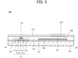
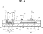
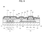
- FIG. 3 to FIG. 6 are cross-sectional views illustrating the method for manufacturing the semiconductor device according to an embodiment of the present invention.
- a semiconductor layer made of polysilicon is formed on a substrate 101, the semiconductor layer is processed by a photolithography process, and the semiconductor layer 111 is formed.
- the gate insulating layer 112 is formed on the substrate 101 and the semiconductor layer 111.
- a conductive layer is formed on the gate insulating layer 112, the conductive layer is processed by the photolithography process, and the gate electrode 113 overlapping the semiconductor layer 111 and the gate electrode 128 included in the transistor 120 are formed.
- an impurity is implanted into the semiconductor layer 111 through the gate insulating layer 112.
- the channel region 111a and other impurity regions are formed.
- a mask covering a region corresponding to the channel region 111a and the low-concentration impurity regions 111b and 111c is formed using a resist or the like, and additional impurities are implanted.
- the source region 111d and the drain region 111e are formed in a region adjacent to the low-concentration impurity regions 111b and 111c by the implantation of additional impurities.
- the low-concentration impurity regions 111b and 111c may be omitted.
- the channel region 111a is adjacent to the source region 111d and the drain region 111e.
- the interlayer insulating layer 114 is formed on the gate electrode 112 and the gate electrodes 113 and 128.
- the oxide semiconductor layer is formed on the interlayer insulating layer 114, the semiconductor layer is processed by the photolithography process, and the oxide semiconductor layer 121 is formed.
- an insulating layer is formed on the interlayer insulating layer 114 and the oxide semiconductor layer 121.
- the insulating layer has a function as the interlayer insulating layer 116 in the transistor 110, and a function as the gate insulation layer 122 in the transistor 120.
- the gate insulating layer 112 and the interlayer insulating layers 114 and 116 are processed by the photolithography process to form the openings 115a, 115b reaching the source region 111d and the drain region 111e of the semiconductor layer 111 and 115c reaching the gate electrode 128.
- a conductive layer is deposited on the interlayer insulating layer 116 and inside the openings 115a, 115b and 115c.
- the source electrode 117a, the drain electrode 117b, the wiring 119 and the gate electrode 123 are formed by processing the deposited conductive layer by the photolithography process.
- an impurity is implanted into the oxide semiconductor layer 121 through the gate insulating layer 122.
- the impurity By implanting the impurity, the channel region 121a, the source region 121d, and the drain region 121e are formed. A method of forming the source region 121d and the drain region 121e will be described later.
- the interlayer insulating layer 126 covering the source electrode 117a, the drain electrode 117b, the wiring 119 and the gate electrode 123 is formed on the interlayer insulating layer 116.
- the openings 127d and 127e that reach the source region 121d and the drain region 121e of the oxide semiconductor layer 121 are formed.
- the metal nitride layer 124 and a conductive layer 125 are deposited on the interlayer insulating layer 126 and inside the openings 127d and 127e.
- the metal nitride layers 124c and 124d, the source electrode 125c, and the drain electrode 125d shown in FIG. 2 are formed by processing the deposited metal nitride layer 124 and the conductive layer 125 by the photolithography process.
- the metal nitride layer 124c is arranged between the oxide semiconductor layer 121 and the source electrode 125c and the metal nitride layer 124d is arranged between the oxide semiconductor layer 121 and the drain electrode 125d, an increase in contact resistance can be suppressed. Further, since the semiconductor layer 111 is in contact with the source electrode 117a and the drain electrode 117b without a metal nitride layer, an increase in contact resistance can be suppressed.
- a method of forming the source region 121d and the drain region 121e will be described with reference to FIG. 4 .
- ion implantation is performed on the oxide semiconductor layer 121 in a state where the gate insulating layer 122 and the gate electrode 123 are formed on the oxide semiconductor layer 121.
- boron (B) is implanted as an impurity element into the oxide semiconductor layer 121 by the ion implantation.
- other impurity elements such as phosphorus (P) may be implanted into the oxide semiconductor layer 121 instead of boron.
- the impurity element passes through the gate insulating layer 122 and reaches the oxide semiconductor layer 121. However, since the impurity element is blocked by the gate electrode 123 in a region (the channel region 121a) where the gate electrode 123 is arranged, the impurity element does not reach the oxide semiconductor layer 121.
- the source region 121d and the drain region 121e in which the impurity element is implanted are formed in the oxide semiconductor layer 121.
- oxygen defects are formed by the implantation of the impurity element. Therefore, the resistance of the oxide semiconductor layer 121 in the source region 121d and the drain region 121e is reduced.
- the source region 121d and the drain region 121e in which the impurity element is implanted may have crystallinity. This is also one of the characteristics of the Poly-OS.
- the crystal structure of each of the source region 121d and the drain region 121e is the same as the crystal structure of the channel region 121a.
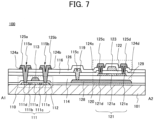
- FIG. 7 is a cross-sectional view when the semiconductor device 100 is cut along a line A1-A2 similar to FIG. 1 .
- the semiconductor device 100 according to an embodiment of the present invention includes the transistor 110 and the transistor 120 arranged on the transistor 110.
- metal nitride layers 124a and 124b are arranged on the interlayer insulating layer 126.
- a source electrode 125a and a drain electrode 125b are arranged on the metal nitride layers 124a and 124b.
- the source electrode 125a and the drain electrode 125b are connected to the source region 111d and the drain region 111e via the openings 115a and 115b arranged in the interlayer insulating layers 114, 116, and 126.
- a material similar to the metal nitride layer 124c and 124d can be used as the metal nitride layers 124a and 124b.
- a material similar to the source electrode 125c and the drain electrode 125d can be used as the source electrode 125a and the drain electrode 125b.
- the metal nitride layers 124a and 124b may be referred to as a "second metal nitride layer", and the source electrode 125a and the drain electrode 125b may be referred to as a "first electrode”.
- the configuration of the semiconductor device 100 can be paraphrased as follows.
- the second insulating layer (the interlayer insulating layer 116) is arranged above the first insulating layer (the interlayer insulating layer 114).
- the openings 115a and 115b are arranged in each of the first insulating layer (the interlayer insulating layer 114) and the second insulating layer (the interlayer insulating layer 116).
- the first electrodes are arranged above the second insulating layer (the interlayer insulating layer 116) and inside the openings 115a and 115b, and are in contact with the first semiconductor layer (the semiconductor layer 111).
- the second metal nitride layers are arranged above the second insulating layer (the interlayer insulating layer 116) between the second insulating layer (the interlayer insulating layer 116) and the first electrodes (the source electrode 125a and the drain electrode 125b).
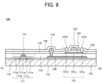
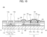
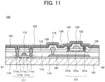
- FIG. 8 to FIG. 11 are cross-sectional views illustrating the method for manufacturing a semiconductor device according to an embodiment of the present invention.
- a semiconductor layer made of polysilicon is formed on the substrate 101, the semiconductor layer is processed by a photolithography process, and the semiconductor layer 111 is formed.
- the gate insulating layer 112 is formed on the substrate 101 and the semiconductor layer 111.
- a conductive layer is formed on the gate insulating layer 112, the conductive layer is processed by the photolithography process, and the gate electrode 113 overlapping the semiconductor layer 111 and the gate electrode 128 included in the transistor 120 are formed.
- an impurity is implanted into the semiconductor layer 111 through the gate insulating layer 112.
- the channel region 111a and other impurity regions are formed.
- a mask covering a region corresponding to the channel region 111a and the low-concentration impurity regions 111b and 111c is formed using a resist or the like, and additional impurities are implanted.
- the source region 111d and the drain region 111e are formed in a region adjacent to the low-concentration impurity regions 111b and 111c by the implantation of additional impurities.
- the low-concentration impurity regions 111b and 111c may be omitted.
- the channel region 111a is adjacent to the source region 111d and the drain region 111e.
- the interlayer insulating layer 114 is formed on the gate insulating layer 112 and the gate electrodes 113 and 128.
- a semiconductor layer is formed on the interlayer insulating layer 114, the semiconductor layer is processed by a photolithography process, and the oxide semiconductor layer 121 is formed.
- an insulating layer is formed on the interlayer insulating layer 114 and the oxide semiconductor layer 121.
- the insulating layer is an insulating layer that functions as the interlayer insulating layer 116 in the transistor 110 and the gate insulating layer 122 in the transistor 120.
- the interlayer insulating layers 114 and 116 are processed by the photolithography process to form the opening 115c reaching the gate electrode 128.
- a conductive layer is deposited on the interlayer insulating layer 116 and inside the opening 115c.
- the wiring 119 and the gate electrode 123 are formed by processing the deposited conductive layer by the photolithography process.
- the interlayer insulating layer 126 is formed on the interlayer insulating layer 116, the wiring 119, and the gate electrode 123.
- the openings 127d and 127e that reach the source region 121d and the drain region 121e of the oxide semiconductor layer 121 are formed.
- the metal nitride layer 124 is formed on the interlayer insulating layer 126 and inside the openings 127d and 127e.
- the deposited metal nitride layer 124, the gate insulating layer 112, and the interlayer insulating layers 114, 116, and 126 are processed by the photolithography process to form the openings 115a and 115b that reach the source region 111d and the drain region 111e of the semiconductor layer 111.
- a conductive layer 125 is deposited on the metal nitride layer 124 and inside the openings 115a and 115b.
- the source electrode 125a and the drain electrode 125b shown in FIG. 7 are formed by processing the deposited conductive layer 125 by the photolithography process.
- the metal nitride layer 124c is arranged between the oxide semiconductor layer 121 and the source electrode 125c and the metal nitride layer 124d is arranged between the oxide semiconductor layer 121 and the drain electrode 125d, an increase in contact resistance can be suppressed. Furthermore, since the semiconductor layer 111 is in contact with the source electrode 125a and the drain electrode 125b without interposing the metal nitride layer, an increase in contact resistance can be suppressed.
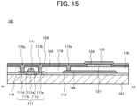
- FIG. 12 to FIG. 15 An example of a structure of the semiconductor device 100 according to an embodiment of the present invention will be described with reference to FIG. 12 to FIG. 15 .
- FIG. 12 is a cross-sectional view when the semiconductor device 100 is cut along a line A1-A2 similar to FIG. 1 .
- the semiconductor device 100 according to an embodiment of the present invention includes the transistor 110 arranged on the substrate 101 and the transistor 120 arranged on the transistor 110.
- a configuration of the transistor 110 shown in FIG. 12 is substantially the same as the configuration of the transistor 110 shown in FIG. 7 .
- the insulating layer arranged between the semiconductor layer 111 and the source electrode 125a (and the drain electrode 125b) is the gate insulating layer 112 and the interlayer insulating layers 114, 116, and 126
- the insulating layer is the gate insulating layer 112 and the interlayer insulating layer 114. That is, in FIG. 12 , the metal nitride layers 124a and 124b are in contact with an upper surface of the interlayer insulating layer 114.
- a metal nitride layer 118 is arranged on the interlayer insulating layer 114.
- the wiring 119 is arranged on the metal nitride layer 118.
- the wiring 119 is connected to the gate electrode 128 via the opening 115c arranged in the interlayer insulating layer 114.
- the metal nitride layer 118 is formed only on an upper surface of the interlayer insulating layer 114, and is not formed on the side walls of the opening 115c and an upper surface of the gate electrode 128.
- the oxide semiconductor layer 121 is arranged on the gate insulating layer 129.
- the metal nitride layers 124c and 124d are arranged on the upper surface and the side surface of the oxide semiconductor layer 121.
- the source electrode 125c and the drain electrode 125d are arranged on the upper surface of the metal nitride layers 124c and 124d.
- the source electrode 125c and the metal nitride layer 124c are arranged in a region including the source region 121d.
- the drain electrode 125d and the metal nitride layer 124d are arranged in a region including the drain region 121e.
- the metal nitride layers 124c and 124d, the source electrode 125c, and the drain electrode 125d are not arranged in the channel region 121a. In other words, the oxide semiconductor layer 121 in the channel region 121a is exposed from the metal nitride layer and the conductive layer formed on the oxide semiconductor layer 121.
- the transistor 120 shown in FIG. 12 a voltage for controlling the channel region 121a is supplied to the gate electrode 128. That is, the transistor 120 is a bottom-gate transistor.
- the above configuration can be paraphrased as follows.
- the first insulating layer (the interlayer insulating layer 114) is in the same layer as the third gate insulating layer (the gate insulating layer 129).
- the first gate electrode (the gate electrode 113) is in the same layer as the third gate electrode (the gate electrode 128).
- the first metal nitride layers (the metal nitride layers 124c and 124d) are in contact with the upper surface and the side surface of the second semiconductor layer (the oxide semiconductor layer 121).
- the openings 115a and 115b are arranged in first insulating layer (the interlayer insulating layer 114).
- the first electrodes are arranged above the first insulating layer (the interlayer insulating layer 114) and inside the openings 115a and 115b, and are in contact with the first semiconductor layer (the semiconductor layer 111).
- the second metal nitride layer (the metal nitride layers 124a and 124b) is arranged above the first insulating layer (the interlayer insulating layer 114) between the first insulating layer (the interlayer insulating layer 114) and the first electrodes (the source electrode 125a and the drain electrode 125b).
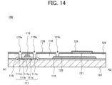
- FIG. 13 to FIG. 15 are cross-sectional views illustrating a method for manufacturing a semiconductor device according to an embodiment of the present invention.
- the manufacturing method shown in FIG. 13 is the same as the manufacturing method shown in FIG. 3 up to the step of forming the oxide semiconductor layer 121, the explanation thereof will be omitted.
- the metal nitride layer 124 is deposited on the interlayer insulating layer 114 and on the oxide semiconductor layer 121.
- the deposited metal nitride layers 124, the gate insulating layer 112, and the interlayer insulating layer 114 are processed by the photolithography process to form the openings 115a, 115b reaching the source region 111d and the drain region 111e of the semiconductor layer 111 and 115c reaching the gate electrode 128.
- the conductive layer 125 is deposited on the metal nitride layers 124 and inside the openings 115a, 115b and 115c.
- the metal nitride layers 124a, 124b, 124c, 124d and 118, the source electrodes 125a and 125c, the drain electrodes 125b and 125d, and the wiring 119 shown in FIG. 12 are formed.
- the metal nitride layer 124c is arranged between the oxide semiconductor layer 121 and the source electrode 125c and the metal nitride layer 124d is arranged between the oxide semiconductor layer 121 and the drain electrode 125d, an increase in contact resistance can be suppressed. Furthermore, since the semiconductor layer 111 is in contact with the source electrode 125a and the drain electrode 125b without interposing the metal nitride layer, an increase in contact resistance can be suppressed.
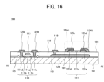
- FIG. 16 to FIG. 19 An example of a structure of the semiconductor device 100 according to an embodiment of the present invention will be described with reference to FIG. 16 to FIG. 19 .
- FIG. 16 is a cross-sectional view when the semiconductor device 100 is cut along a line A1-A2 similar to FIG. 1 .
- the semiconductor device 100 according to an embodiment of the present invention includes the transistor 110 and the transistor 120 arranged on the transistor 110.
- a configuration of the transistors 110 and 120 shown in FIG. 16 is similar to the configuration of each of the transistors 110 and 120 shown in FIG. 12 , the configurations are different from each other in the region where the metal nitride layers are arranged.
- the metal nitride layers 124a and 124b are arranged between the source electrode 125a and the interlayer insulating layer 114, and between the drain electrode 125b and the interlayer insulating layer 114.
- the metal nitride layer is not arranged in the same position as described above. That is, the source electrode 125a and the drain electrode 125b are in contact with the upper surface of the interlayer insulating layer 114.
- the metal nitride layer 118 is arranged between the wiring 119 and the interlayer insulating layer 114, but in the transistor 120 shown in FIG. 16 , the metal nitride layer is not arranged in the same position as described above. That is, the source electrode 125a and the drain electrode 125b are in contact with the upper surface of the interlayer insulating layer 114.
- the metal nitride layers 124c and 124d are formed from the upper surface of the oxide semiconductor layer 121 to the upper surface of the interlayer insulating layer 114 beyond the side surface of the oxide semiconductor layer 121, but in the transistor 120 shown in FIG. 16 , the metal nitride layers 124c and 124d are formed only on the upper surface of the oxide semiconductor layer 121. That is, the metal nitride layers 124c and 124d are not formed on the side surface of the oxide semiconductor layer 121.
- the side surface of the oxide semiconductor layer 121 is in contact with the source electrode 125c and the drain electrode 125d arranged above the metal nitride layers 124c and 124d.
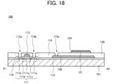
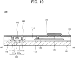
- FIG. 17 to FIG. 19 are cross-sectional views illustrating a method for manufacturing a semiconductor device according to an embodiment of the present invention.
- the manufacturing method shown in FIG. 17 is the same as the manufacturing method shown in FIG. 3 up to the step of forming the interlayer insulating layer 114, the explanation thereof will be omitted.
- the oxide semiconductor layer 121 and the metal nitride layer 124 are deposited on the interlayer insulating layer 114.
- the deposited oxide semiconductor layer 121 and the metal nitride layer 124 are processed by a photolithography process.
- the gate insulating layer 112 and the interlayer insulating layer 114 are processed by the photolithography process to form the openings 115a and 115b reaching the source region 111d and the drain region 111e of the semiconductor layer 111 and the opening 115c reaching the gate electrode 128.
- the conductive layer 125 is deposited on the metal nitride layer 124 and inside the openings 115a, 115b, and 115c.
- the deposited conductive layer 125 is processed by the photolithography process to form the metal nitride layers 124c and 124d, the source electrodes 125a and 125c, the drain electrodes 125b and 125d, and the wiring 119 shown in FIG. 16 .
- the metal nitride layer 124c is arranged between the oxide semiconductor layer 121 and the source electrode 125c and the metal nitride layer 124d is arranged between the oxide semiconductor layer 121 and the drain electrode 125d, an increase in contact resistance can be suppressed. Furthermore, since the semiconductor layer 111 is in contact with the source electrode 125a and the drain electrode 125b without interposing the metal nitride layer, an increase in contact resistance can be suppressed.
- FIG. 20 An example of a structure of the semiconductor device 100 according to an embodiment of the present invention will be described with reference to FIG. 20 .
- FIG. 20 is a cross-sectional view when the semiconductor device 100 is cut along a line A1-A2 similar to FIG. 1 .
- the semiconductor device 100 according to an embodiment of the present invention includes the transistor 110 arranged on the substrate 101 and the transistor 120 arranged on the transistor 110.
- a configuration of the transistor 120 shown in FIG. 20 is similar to the configuration of each of the transistors 120 shown in FIG. 12 , but is different from the transistor 120 shown in FIG. 12 in that the gate electrode 123 is arranged above the oxide semiconductor layer 121.
- a voltage for controlling the channel region 121a is supplied to the gate electrodes 123 and 128. That is, the transistor 120 is a dual-gate transistor.
- the voltage for controlling the channel region 121a may not be supplied to the gate electrode 128, and a predetermined fixed voltage may be supplied to the gate electrode 128.
- the gate electrode 128 may be floating.
- the transistor 120 may be a top-gate transistor in which the gate electrode 128 is omitted and the voltage for controlling the channel region 121a is supplied to the gate electrode 123.
- the transistor 120 shown in FIG. 20 is obtained by forming the interlayer insulating layer 126 on the transistor 120 shown in FIG. 12 , forming the conductive layer on the interlayer insulating layer 126, and processing the conductive layer into the gate electrode 123 by the photolithography process.
- the interlayer insulating layer 126 functions as the gate insulating layer.
Landscapes
- Physics & Mathematics (AREA)
- Geometry (AREA)
- Engineering & Computer Science (AREA)
- Microelectronics & Electronic Packaging (AREA)
- Thin Film Transistor (AREA)
Abstract
Description
- An embodiment of the present invention relates to a semiconductor device.
- In recent years, a semiconductor device has been developed in which transistors made of different semiconductor materials are formed on the same substrate as a semiconductor layer. For example, a transistor using silicon is used as a transistor requiring high-speed operation, and a transistor using an oxide semiconductor is used as a transistor requiring a switching operation, so that transistors having different characteristics depending on a required function can be formed on the same substrate.
- Patent Literature 1 discloses a display device in which a transistor in which silicon is used for a driving circuit is formed on the same substrate, and a transistor in which an oxide semiconductor is used for a display region is formed.
- Patent Literature 1:
Japanese laid-open patent publication No. 2018-128693 - An object of an embodiment of the present invention is to provide a highly productive semiconductor device that achieves good characteristics for each transistor having different characteristics.
- A semiconductor device according to an embodiment of the present invention includes: a first semiconductor layer; a first gate electrode facing the first semiconductor layer; a first gate insulating layer between the first semiconductor layer and the first gate electrode; a first insulating layer arranged above the first gate electrode; a first electrode arranged in a region overlapping the first semiconductor layer in a plan view, and electrically connected to the first semiconductor layer; a second semiconductor layer arranged above the first insulating layer and made of a different material from the first semiconductor layer; a second gate electrode facing the second semiconductor layer; a second gate insulating layer between the second semiconductor layer and the second gate electrode; a second electrode arranged in a region overlapping the second semiconductor layer in a plan view, and electrically connected to the second semiconductor layer; and/or a first metal nitride layer between the second semiconductor layer and the second electrode, wherein the second semiconductor layer is polycrystalline, and an etching rate of the second semiconductor layer with respect to an etchant including phosphoric acid as a main component is less than 3 nm/min at 40 ° C. Further, the content of
JP2023-169618 -
-
FIG. 1 is a plan view illustrating a semiconductor device according to an embodiment of the present invention. -
FIG. 2 is a cross-sectional view illustrating a semiconductor device according to an embodiment of the present invention. -
FIG. 3 is a cross-sectional view illustrating a method for manufacturing a semiconductor device according to an embodiment of the present invention. -
FIG. 4 is a cross-sectional view illustrating a method for manufacturing a semiconductor device according to an embodiment of the present invention. -
FIG. 5 is a cross-sectional view illustrating a method for manufacturing a semiconductor device according to an embodiment of the present invention. -
FIG. 6 is a cross-sectional view illustrating a method for manufacturing a semiconductor device according to an embodiment of the present invention. -
FIG. 7 is a cross-sectional view illustrating a semiconductor device according to an embodiment of the present invention. -
FIG. 8 is a cross-sectional view illustrating a method for manufacturing a semiconductor device according to an embodiment of the present invention. -
FIG. 9 is a cross-sectional view illustrating a method for manufacturing a semiconductor device according to an embodiment of the present invention. -
FIG. 10 is a cross-sectional view illustrating a method for manufacturing a semiconductor device according to an embodiment of the present invention. -
FIG. 11 is a cross-sectional view illustrating a method for manufacturing a semiconductor device according to an embodiment of the present invention. -
FIG. 12 is a cross-sectional view illustrating a semiconductor device according to an embodiment of the present invention. -
FIG. 13 is a cross-sectional view illustrating a method for manufacturing a semiconductor device according to an embodiment of the present invention. -
FIG. 14 is a cross-sectional view illustrating a method for manufacturing a semiconductor device according to an embodiment of the present invention. -
FIG. 15 is a cross-sectional view illustrating a method for manufacturing a semiconductor device according to an embodiment of the present invention. -
FIG. 16 is a cross-sectional view illustrating a semiconductor device according to an embodiment of the present invention. -
FIG. 17 is a cross-sectional view illustrating a method for manufacturing a semiconductor device according to an embodiment of the present invention. -
FIG. 18 is a cross-sectional view illustrating a method for manufacturing a semiconductor device according to an embodiment of the present invention. -
FIG. 19 is a cross-sectional view illustrating a method for manufacturing a semiconductor device according to an embodiment of the present invention. -
FIG. 20 is a cross-sectional view illustrating a semiconductor device according to an embodiment of the present invention. - Hereinafter, embodiments of the present invention will be described with reference to the drawings. The following disclosure is merely an example. A configuration that can be easily conceived by a person skilled in the art by appropriately changing the configuration of the embodiment while keeping the gist of the invention is naturally included in the scope of the present invention. For clarity of explanation, the drawings may be schematically represented with respect to widths, thicknesses, shapes, and the like of respective portions as compared with actual embodiments. However, the illustrated shapes are merely examples, and do not limit the interpretation of the present invention. In the present specification and the drawings, the same reference signs are given to the same components as those described above with respect to the above-described drawings, and detailed description thereof may be omitted as appropriate.
- In the embodiments of the present invention, a direction from a substrate toward an oxide semiconductor layer is referred to as upper or above. Conversely, a direction from the oxide semiconductor layer to the substrate is referred to as lower or below. In this way, for convenience of explanation, the phrase "above" or "below" is used for explanation, but for example, the vertical relationship between the substrate and the oxide semiconductor layer may be different from that shown in the drawings. In the following explanation, for example, the expression "oxide semiconductor layer on a substrate" merely describes the vertical relationship between the substrate and the oxide semiconductor layer as described above, and another member may be arranged between the substrate and the oxide semiconductor layer. The terms "above" or "below" mean a stacking order in a structure in which a plurality of layers is stacked, and when expressed as a pixel electrode above a transistor, it may be a positional relationship in which the transistor and the pixel electrode do not overlap in a plan view. On the other hand, when expressed as a pixel electrode vertically above a transistor, it means a positional relationship in which the transistor and the pixel electrode overlap in a plan view.
- In the present specification, the terms "film" and "layer" can optionally be interchanged with one another.
- "Display device" refers to a structure that displays an image using an electro-optic layer. For example, the term "display device" may refer to a display panel that includes the electro-optic layer, or may refer to a structure with other optical members (for example, a polarized member, a backlight, a touch panel, and the like) attached to a display cell. "Electro-optical layer" may include a liquid crystal layer, an electroluminescent (EL) layer, an electrochromic (EC) layer, or an electrophoretic layer, as long as no technical contradiction is caused. Therefore, although a display device will be described by exemplifying a liquid crystal display device including a liquid crystal layer and an organic EL display device including an organic EL layer for the embodiments described later, the structure according to the present embodiment can be applied to a display device including other electro-optical layers described above.
- In the present specification, the expressions "α includes A, B, or C," "α includes any of A, B, and C," and "α includes one selected from a group consisting of A, B, and C," do not exclude the case where α includes a plurality of combinations of A to C unless otherwise specified. Furthermore, these expressions do not exclude the case where α includes other elements.
- The following embodiments can be combined with each other as long as there is no technical contradiction.
- An example of a structure of a
semiconductor device 100 according to an embodiment of the present invention will be described with reference toFIG. 1 to FIG. 6 . -
FIG. 1 is a plan view of thesemiconductor device 100 according to an embodiment of the present invention.FIG. 2 is a cross-sectional view when thesemiconductor device 100 shown inFIG. 1 is cut along a line A1-A2. As shown inFIG. 1 andFIG. 2 , thesemiconductor device 100 according to an embodiment of the present invention includes atransistor 110 and atransistor 120 arranged on thetransistor 110. - The
transistor 110 includes asemiconductor layer 111, agate insulating layer 112, and agate electrode 113. - Either an N-type transistor or a P-type transistor may be used as the
transistor 110. In the present embodiment, an example in which a top-gate type N-type transistor in which polysilicon is used for a semiconductor layer is used as thetransistor 110 will be described. - The
semiconductor layer 111 in the N-type transistor includes achannel region 111a, asource region 111d, adrain region 111e, and low-concentration impurity regions concentration impurity region 111b is arranged between thechannel region 111a and thesource region 111d. The low-concentration impurity region 111c is arranged between thechannel region 111a and thedrain region 111e. The source and the drain may be interchanged depending on the operation of thetransistor 110. That is, theregion 111d may function as the drain region, and theregion 111e may function as the source region. - The
semiconductor layer 111 in thechannel region 111a has semiconductor properties. That is, depending on a voltage applied to thegate electrode 113, thesemiconductor layer 111 in thechannel region 111a is switched between a state functioning as a current path and a state not functioning as a current path. The carrier concentration in thesemiconductor layer 111 in thesource region 111d and thedrain region 111e is greater than the carrier concentration in thesemiconductor layer 111 in thechannel region 111a. -
Interlayer insulating layers transistor 110. Asource electrode 117a and adrain electrode 117b are arranged on theinterlayer insulating layers source electrode 117a and thedrain electrode 117b are connected to thesource region 111d and thedrain region 111e viaopenings interlayer insulating layers - The
transistor 120 is arranged in a region different from a region where thetransistor 110 is arranged. Thetransistor 120 includes anoxide semiconductor layer 121, agate insulating layer 122, agate electrode 123, agate electrode 128, and agate insulating layer 129. An interlayer insulatinglayer 126 is arranged on thegate electrode 123. Although details will be described later, theoxide semiconductor layer 121 is polycrystalline. - The
gate electrode 128 is arranged between thegate insulating layer 112 and the interlayer insulatinglayer 114. Thegate electrode 128 is arranged in a region that overlaps the oxide semiconductor layer 121 (in particular, achannel region 121a) in a plan view. Awiring 119 is arranged on theinterlayer insulating layers wiring 119 is connected to thegate electrode 128 via anopening 115c arranged in each of theinterlayer insulating layers wiring 119 is in the same layer as thesource electrode 117a and thedrain electrode 117b. In other words, thewiring 119 is in contact with the interlayer insulatinglayer 116 in the same manner as thesource electrode 117a and thedrain electrode 117b. - The
channel region 121a, asource region 121d, and adrain region 121e are arranged in theoxide semiconductor layer 121. Thesource region 121d and thedrain region 121e are adjacent to thechannel region 121a. In a plan view, thechannel region 121a overlaps thegate electrode 123. - The
oxide semiconductor layer 121 of thechannel region 121a has semiconductor properties. That is, depending on a voltage applied to thegate electrodes oxide semiconductor layer 121 of thechannel region 121a is switched between a state functioning as a current path and a state not functioning as a current path. The carrier concentration in theoxide semiconductor layer 121 in thesource region 121d and thedrain region 121e is greater than the carrier concentration in theoxide semiconductor layer 121 in thechannel region 121a. - For example, the sheet resistance of the
oxide semiconductor layer 121 in thesource region 121d and thedrain region 121e is 1000 Ω/sq. or less, preferably 500 Ω/sq. or less, and more preferably 250 Ω/sq. or less. In other words, theoxide semiconductor layer 121 in thechannel region 121a has a higher electrical resistance (or lower electrical conductivity) than theoxide semiconductor layer 121 in each of thesource region 121d and thedrain region 121e. - A voltage for controlling the
channel region 121a is supplied to thegate electrodes transistor 120. However, thetransistor 120 may be a bottom-gate transistor in which only thegate electrode 128 is arranged, or may be a top-gate transistor in which only thegate electrode 123 is arranged. -
Openings source region 121d and thedrain region 121e of theoxide semiconductor layer 121 are arranged in thegate insulating layer 122 and the interlayer insulatinglayer 126. Metal nitride layers 124c and 124d are arranged inside theopening 127d, inside theopening 127e, and on thesource region 121d and thedrain region 121e. The metal nitride layers 124c and 124d are in contact with an upper surface of theoxide semiconductor layer 121 and an upper surface of the interlayer insulatinglayer 126. Thesource electrode 125c and thedrain electrode 125d are arranged inside theopening 127d, inside theopening 127e, and on the metal nitride layers 124c and 124d. - With regards to the above configuration, the
semiconductor layer 111 may be referred to as a "first semiconductor layer", thegate electrode 113 may be referred to as a "first gate electrode", thegate insulating layer 112 may be referred to as a "first gate insulating layer", theinterlayer insulating layer 114 may be referred to as a "first insulating layer", and thesource electrode 117a and thedrain electrode 117b may be referred to as a "first electrode". Similarly, theoxide semiconductor layer 121 may be referred to as a "second semiconductor layer", thegate electrode 123 may be referred to as a "second gate electrode", thegate insulating layer 122 may be referred to as a "second gate insulating layer", thegate electrode 128 may be referred to as a "third gate electrode", thegate insulating layer 129 may be referred to as a "third gate insulating layer", the metal nitride layers 124c and 124d may be referred to as a "first metal nitride layer", and thesource electrode 125c and thedrain electrode 125d may be referred to as a "second electrode". Similarly, theinterlayer insulating layer 116 may be referred to as a "second insulating layer." On the other hand, unlike the above, thegate electrode 123 may be referred to as a "third gate electrode", thegate insulating layer 122 may be referred to as a "third gate insulating layer", thegate electrode 128 may be referred to as a "second gate electrode", and thegate insulating layer 129 may be referred to as a "second gate insulating layer". - When expressed as described above, a configuration of
semiconductor device 100 can be paraphrased as follows. The first gate electrode (the gate electrode 113) faces the first semiconductor layer (the semiconductor layer 111). The first gate insulating layer (the gate insulating layer 112) is present between the first semiconductor layer (the semiconductor layer 111) and the first gate electrode (the gate electrode 113). The first insulating layer (the interlayer insulating layer 114) is arranged above the first gate electrode (the gate electrode 113). The first electrodes (thesource electrode 117a and thedrain electrode 117b) are arranged in a region overlapping the first semiconductor layer (the semiconductor layer 111) in a plan view and are electrically connected to the first semiconductor layer (the semiconductor layer 111). The second semiconductor layer (the oxide semiconductor layer 121) is made of a material different from that of the first semiconductor layer (the semiconductor layer 111). The second semiconductor layer (the oxide semiconductor layer 121) is arranged above the first insulating layer (the interlayer insulating layer 114). The second gate electrode (the gate electrode 123) faces the second semiconductor layer (the oxide semiconductor layer 121) below the second semiconductor layer (the oxide semiconductor layer 121). The second gate insulating layer (the gate insulating layer 122) is present between the second semiconductor layer (the oxide semiconductor layer 121) and the second gate electrode (the gate electrode 123). The second electrodes (thesource electrode 125c and thedrain electrode 125d) are arranged in a region overlapping the second semiconductor layer (the oxide semiconductor layer 121) in a plan view and are electrically connected to the second semiconductor layer (the oxide semiconductor layer 121). The first metal nitride layers (the metal nitride layers 124c and 124d) are present between the second semiconductor layer (the oxide semiconductor layer 121) and the second electrodes (thesource electrode 125c and thedrain electrode 125d). - Similarly, the configuration of the
semiconductor device 100 can be rephrased as follows. The first metal nitride layers (the metal nitride layers 124c and 124d) are in contact with the second semiconductor layer (the oxide semiconductor layer 121). The second insulating layer (the interlayer insulating layer 116) is arranged above the first insulating layer (the interlayer insulating layer 114). The third gate electrode (128) faces the second semiconductor layer (the oxide semiconductor layer 121) below the first insulating layer (the interlayer insulating layer 114). The third gate insulating layer (the gate insulating layer 129) is present between the second semiconductor layer (the oxide semiconductor layer 121) and the third gate electrode (the gate electrode 128). The second gate electrode (the gate electrode 123) is arranged above the second insulating layer (the interlayer insulating layer 116). Theopenings source electrode 117a and thedrain electrode 117b) are arranged above the second insulating layer (the interlayer insulating layer 116) and inside theopenings source electrode 117a and thedrain electrode 117b) are in the same layer as the second gate electrode (the gate electrode 123). - Conventionally, in the case where a transistor in which a poly silicon is used and a transistor in which an oxide semiconductor is used is formed on the same substrate, the following problem has arisen. In the case where the conductive layer in contact with the oxide semiconductor is processed into a desired shape, a surface of the oxide semiconductor may be damaged. The oxide semiconductor of the damaged region contains many oxygen vacancies. When an oxygen vacancy occurs in the oxide semiconductor, the off-leakage current of the transistor increases. In order to solve this problem, it is necessary to introduce a sufficient amount of oxygen into the oxide semiconductor by a heat treatment. However, this heat treatment causes the source electrode and the drain electrode to react with the oxide semiconductor, thereby reducing the on-state current of the transistor. Therefore, in an embodiment of the present invention, the metal nitride layer is arranged between the oxide semiconductor layer and the source electrode and between the oxide semiconductor layer and the drain electrode. The metal nitride layer suppresses the reaction between the oxide semiconductor and the electrode due to the heat treatment.
- On the other hand, in the case where the metal nitride layer is arranged between the polysilicon and the source electrode and between the polysilicon and the drain electrode, nitrogen is implanted into the polysilicon when the metal nitride layer is deposited. This increases the contact resistance between the source and drain electrodes and the polysilicon via the metal nitride layer. According to an embodiment of the present invention, a structure in which the metal nitride layer is arranged only in the transistor in which an oxide semiconductor is used is exemplified. That is, the polysilicon is in direct contact with the source electrode and the drain electrode without interposing the metal nitride layer. On the other hand, the oxide semiconductor is connected to the source electrode and the drain electrode via the metal nitride layer. As a result, good characteristics can be obtained for each transistor.
- A rigid substrate having light transmittance such as a glass substrate, a quartz substrate, a sapphire substrate, or the like, is used as the
substrate 101. In the case where thesubstrate 101 needs to have flexibility, a substrate containing a resin such as a polyimide substrate, an acryl substrate, a siloxane substrate, or a fluororesin substrate is used as thesubstrate 101. In the case where the substrate containing a resin is used as thesubstrate 101, an impurity may be introduced into the resin in order to improve the heat resistance of thesubstrate 101. In particular, in the case where thesemiconductor device 100 is a top-emission display, thesubstrate 101 does not need to be transparent, so that an impurity that degrades the transparency of thesubstrate 101 may be used. In the case where thesemiconductor device 100 is used in an integrated circuit other than a display device, a semiconductor substrate such as a silicon substrate, a silicon carbide substrate, and a compound semiconductor substrate, or a substrate that does not have light transmittance such as a conductive substrate such as a stainless substrate is used as thesubstrate 101. - For example, low-temperature polysilicon, amorphous silicon, or single-crystal silicon is used as the
semiconductor layer 111. - A common metal material is used as the conductive layer including the
gate electrode 113, thesource electrode 117a, thedrain electrode 117b, thewiring 119, thegate electrodes source electrode 125c, and thedrain electrode 125d. For example, aluminum (Al), titanium (Ti), chromium (Cr), cobalt (Co), nickel (Ni), molybdenum (Mo), hafnium (Hf), tantalum (Ta), tungsten (W), bismuth (Bi), silver (Ag), copper (Cu), and an alloy or compound thereof can be used. The above-described material may be used in a single layer or stacked layer as the conductive layer. - A common insulating material is used as the insulating layer including the
gate insulating layer 112, theinterlayer insulating layers gate insulating layers - An insulating layer having a function of releasing oxygen by a heat treatment is used as the
interlayer insulating layer 126. That is, an oxide insulating layer excessively containing oxygen is used as theinterlayer insulating layer 126. For example, the temperature of the heat treatment in which theinterlayer insulating layer 126 releases oxygen is 600°C or lower, 500°C or lower, 450°C or lower, or 400°C or lower. That is, for example, theinterlayer insulating layer 126 releases oxygen at a heat treatment temperature performed in the manufacturing process of thesemiconductor device 100 in the case where a glass substrate is used as thesubstrate 101. - An insulating layer with few defects is used as the
gate insulating layers gate insulating layers gate insulating layers gate insulating layers gate insulating layers layer 126, the composition ratio of oxygen in the silicon oxide used as thegate insulating layers interlayer insulating layer 126. For example, a layer in which no defects are observed when evaluated by an electron-spin resonance method (ESR) may be used as thegate insulating layers - SiOxNy and AlOxNy are a silicon compound and aluminum compound containing a smaller proportion (x > y) of nitrogen (N) than oxygen (O). SiNxOy and AlNxOy are a silicon compound and aluminum compound containing a smaller proportion (x > y) of oxygen than nitrogen.
- A metal oxide having semiconductor properties may be used as the
oxide semiconductor layer 121. For example, an oxide semiconductor containing indium (In), gallium (Ga), zinc (Zn), and oxygen (O) may be used as theoxide semiconductor layer 121. For example, an oxide semiconductor having a composition ratio of In : Ga : Zn : O = 1 : 1 : 1 : 4 may be used as theoxide semiconductor layer 121. However, the oxide semiconductor containing In, Ga, Zn and O used in the present embodiment is not limited to the above-described composition. An oxide semiconductor having a composition other than the above may be used as the oxide semiconductor. For example, an oxide semiconductor layer having a higher ratio of In than those described above may be used to improve mobility. On the other hand, in order to increase a bandgap and reduce the influence of light irradiation, an oxide semiconductor layer having a larger ratio of Ga than those described above may be used. - An oxide semiconductor containing two or more metals including indium (In) may be used as the
oxide semiconductor layer 121. In this case, in theoxide semiconductor layer 121, the ratio of the indium element to the total amount of metal elements may be 50% or more in atomic ratio. Gallium (Ga), zinc (Zn), aluminum (Al), hafnium (Hf), yttrium (Y), zirconia (Zr), and lanthanoids may be used as theoxide semiconductor layer 121 in addition to indium. Elements other than those described above may be used as theoxide semiconductor layer 121. - Other elements may be added to the oxide semiconductor containing In, Ga, Zn, and O as the
oxide semiconductor layer 121, and metal elements such as Al and Sn may be added. In addition to the above oxide semiconductor, an oxide semiconductor (IGO) containing In and Ga, an oxide semiconductor (IZO) containing In and Zn, an oxide semiconductor (ITZO) containing In, Sn, and Zn, and an oxide semiconductor containing In and W may be used as theoxide semiconductor layer 121. - In the case where the ratio of the indium element is large, the
oxide semiconductor layer 121 is easily crystallized. As described above, theoxide semiconductor layer 121 having a polycrystalline structure can be obtained by using a material in which the ratio of the indium element to the total amount of metal elements is 50% or more. Theoxide semiconductor layer 121 preferably contains gallium as a metal element other than indium. Gallium belongs to the same Group 13 element as indium. Therefore, the crystallinity of theoxide semiconductor layer 121 is not inhibited by gallium, and theoxide semiconductor layer 121 has a polycrystalline structure. - Although a detailed method for manufacturing the
oxide semiconductor layer 121 will be described later, theoxide semiconductor layer 121 can be formed using a sputtering method. A composition of theoxide semiconductor layer 121 formed by the sputtering method depends on a composition of a sputtering target. Even when theoxide semiconductor layer 121 has a polycrystalline structure, the composition of the sputtering target substantially matches the composition of theoxide semiconductor layer 121. In this case, a composition of the metal element of theoxide semiconductor layer 121 can be specified based on a composition of the metal element of the sputtering target. - In the case where the
oxide semiconductor layer 121 has a polycrystalline structure, the composition of the oxide semiconductor layer may be identified using an X-ray diffraction (XRD) method. Specifically, the composition of the metal element of the oxide semiconductor layer can be specified based on the crystalline structure and the lattice constant of the oxide semiconductor layer obtained by the XRD method. Furthermore, the composition of the metal element of theoxide semiconductor layer 121 can also be identified using a fluorescent X-ray analysis, or Electron Probe Micro Analyzer (EPMA) analysis, or the like. However, the oxygen element contained in theoxide semiconductor layer 121 may not be identified by these methods because the oxygen element varies depending on the sputtering process conditions. - As described above, the
oxide semiconductor layer 121 may include an amorphous structure and may include a polycrystalline structure. The oxide semiconductor having a polycrystalline structure can be manufactured using a Poly-OS (Poly-crystalline Oxide Semiconductor) technique described below. In the following explanation, when distinguishing from the oxide semiconductor having an amorphous structure, the oxide semiconductor having a polycrystalline structure may be described as the Poly-OS. - Furthermore, instead of the
oxide semiconductor layer 121, a semiconductor other than the oxide semiconductor may be used. In this case, the semiconductor used in place of the oxide semiconductor may be made of a different material or have a different composition from the semiconductor used in thesemiconductor layer 111. That is, thetransistor 110 has different characteristics from thetransistor 120. - A metal oxide layer may be arranged between the
gate insulating layer 129 and theoxide semiconductor layer 121. In this case, the metal oxide layer may be in contact with theoxide semiconductor layer 121. A metal oxide containing aluminum as a main component is used as the metal oxide layer. For example, an inorganic insulating layer such as aluminum oxide (AlOx), aluminum oxynitride (AlOxNy), and aluminum oxynitride (AlNxOy) is used as the metal oxide layer. The "metal oxide layer containing aluminum as a main component" means that the proportion of aluminum contained in the metal oxide layer is 1% or more of the entire metal oxide layer. The proportion of aluminum contained in the metal oxide layer may be 5% or more and 70% or less, 10% or more and 60% or less, or 30% or more and 50% or less of the entire metal oxide layer. The ratio may be a mass ratio or a weight ratio. - A nitride of a common metal material is used as the metal nitride layers 124c and 124d. For example, titanium nitride, molybdenum nitride, tungsten nitride, and tantalum nitride are used as the metal nitride layers 124c and 124d. The metal nitride layers 124c and 124d contain the same metal elements as the metal element contained in the
source electrode 125c and thedrain electrode 125d. For example, in the case where the structure of thesource electrode 125c and thedrain electrode 125d is Al/Ti (upper layer/lower layer), the metal nitride layers 124c and 124d may be titanium nitride. - In this case, the lower layer (Ti) included in the
source electrode 125c and thedrain electrode 125d (second electrode) may be referred to as a "first conductive layer", and the upper layer (Al) thereof may be referred to as a "second conductive layer". When expressed as described above, the configuration of thesemiconductor device 100 can be paraphrased as follows. The second electrodes (thesource electrode 125c and thedrain electrode 125d) include the first conductive layer (Ti) and the second conductive layer (Al) on the first conductive layer (Ti). The first conductive layer (Ti) is in contact with the first metal nitride layers (metal nitride layer metal nitride layer - The Poly-OS contained in the oxide semiconductor layer is formed using sputtering and a heat treatment. Here, a method for forming the oxide semiconductor layer will be described.
- First, the oxide semiconductor layer is deposited by sputtering. The deposited oxide semiconductor layer has an amorphous structure. In this case, the amorphous structure means a structure in which a long-range ordered structure does not exist and a periodic crystal lattice arrangement is not observed. For example, when the oxide semiconductor layer having an amorphous structure is observed using the XRD method, a certain peak based on the crystalline structure cannot be obtained in the diffractive pattern. The oxide semiconductor layer having an amorphous structure may have a short-range ordered structure in a micro region. However, such an oxide semiconductor layer does not exhibit characteristics of the Poly-OS and can therefore be classified as an oxide semiconductor layer having an amorphous structure.
- In the Poly-OS techniques, the oxide semiconductor layer is deposited at a low temperature. For example, a temperature of a substrate on which the oxide semiconductor layer is deposited is 150°C or lower, preferably 100°C or lower, and more preferably 50°C or lower. When the temperature of the substrate is high during the deposition of the oxide semiconductor layer, microcrystals are likely to be generated in the oxide semiconductor to be deposited. The oxygen partial pressure in a chamber during deposition is 1% or more and 10% or less, preferably 1% or more and 5% or less, and more preferably 2% or more and 4% or less. When the oxygen partial pressure is high, microcrystals are generated in the oxide semiconductor layer due to excess oxygen contained in the oxide semiconductor. On the other hand, under the condition where the oxygen partial pressure is less than 1%, the composition of oxygen in the oxide semiconductor layer becomes uneven, and an oxide semiconductor layer containing a large amount of microcrystals or an oxide semiconductor layer which does not crystallize even when subjected to a heat treatment is formed.
- Next, a heat treatment is performed on the oxide semiconductor layer deposited by sputtering. The heat treatment is performed in the atmosphere, but the atmosphere of the heat treatment is not limited to this. The temperature of the heat treatment is 300°C or higher and 500°C or lower, preferably 350°C or higher and 450°C or lower. The time of the heat treatment is 15 minutes or more and 120 minutes or less, preferably 30 minutes or more and 60 minutes or less. By performing the heat treatment, the oxide semiconductor layer having an amorphous structure is crystallized to form the oxide semiconductor layer containing the Poly-OS.
- Next, the characteristics of the oxide semiconductor layer used as the
oxide semiconductor layer 121 and containing the Poly-OS will be described below. - The oxide semiconductor layer has excellent etching resistance. Specifically, the oxide semiconductor layer has a very low etching rate when etching using an etchant during wet etching. This means that the oxide semiconductor layer is hardly etched by the etchant. When the oxide semiconductor layer is etched at about 40°C using an etchant containing phosphoric acid as a main component, the etching rate is less than 3 nm/min, less than 2 nm/min, or less than 1 nm/min. The proportion of phosphoric acid in the etchant is 50% or more, 60% or more, or 70% or more. The etchant may contain nitric acid and acetic acid in addition to phosphoric acid. The temperature of about 40°C is a set temperature of a device holding the etchant, and the actual temperature of the etchant is 35°C or higher and 45°C or lower.
- On the other hand, in the case where the oxide semiconductor layer is etched using the etchant containing phosphoric acid as a main component at a temperature of about 40°C with respect to an oxide semiconductor layer containing no Poly-OS, for example, the oxide semiconductor layer having an amorphous structure before the heat treatment, the etching rate is 100 nm/min or more.
- In the case where the oxide semiconductor layer containing the Poly-OS is etched using 0.5% of a hydrofluoric acid solution at room temperature (for example, about 22°C), the etching rate is less than 5 nm/min, less than 4 nm/min, or less than 3 nm/min. In this case, the room temperature is 25°C±5°C. The actual temperature of the etchant at this time is 20°C or higher and 30°C or lower.
- On the other hand, in the case where the oxide semiconductor layer containing no Poly-OS is etched using 0.5% of the hydrofluoric acid solution at room temperature, the etching rate is 15 nm/min or more.
- Here, an embodiment of the oxide semiconductor layer is shown in Table 1. Table 1 shows the etching rates for a mixed acid etching solution and 0.5% of the hydrofluoric acid solution for each of the prepared samples. "Mixed acid AT-2F (product name)" manufactured by Rasa Industries, Ltd. was used as the mixed acid etching solution. The proportion of phosphoric acid in the mixed acid etching solution is about 65%. When each sample was etched, the temperature of the mixed acid etching solution was about 40°C and the temperature of 0.5% of the hydrofluoric acid solution was room temperature. In Table 1, Sample 1 is the oxide semiconductor layer containing the Poly-OS, Sample 2 is the oxide semiconductor layer having an amorphous structure before the heat treatment, and Sample 3 is an oxide semiconductor layer containing indium gallium zinc oxide (IGZO) with an indium ratio of less than 50%.
Table 1 Mixed acid etching solution 0.5% hydrofluoric acid solution Sample 1 < 0. 1 nm/min < 2 nm/min Sample 2 111 nm/min > 18 nm/min Sample 3 162 nm/min - - As shown in Table 1, Sample 1 (the oxide semiconductor layer containing the Poly-OS) is hardly etched by the mixed acid etching solution, and only 2 nm/min is etched using 0.5% of the hydrofluoric acid solution. With respect to the mixed acid etching solution, the etching rate of Sample 1 is 1/100 or less of the etching rate of Sample 2 (the oxide semiconductor layer having an amorphous structure before the heat treatment). With respect to 0.5% of the hydrofluoric acid solution, the etching rate of Sample 1 is about 1/10 or less of the etching rate of Sample 2. With respect to the mixed acid etching solution, the etching rate of Sample 1 is 1/100 or less of the etching rate of Sample 3 (the oxide semiconductor layer containing IGZO with an indium ratio of less than 50%). That is, Sample 1 has significantly better etching resistance than Sample 2 and Sample 3.
- Such excellent etching resistance of the oxide semiconductor layer containing Poly-OS is a property that cannot be obtained in the oxide semiconductor having a polycrystalline structure manufactured by the conventional process at 500°C or lower. Although the detailed mechanism for the excellent etching resistance of the oxide semiconductor layer containing the Poly-OS is unclear, the Poly-OS is considered to have a polycrystalline structure different from that of the conventional one.
- As discussed above, the etching rate of the oxide semiconductor layer containing the Poly-OS to the etchant is very low. Therefore, it is very difficult to pattern the oxide semiconductor layer. Therefore, in the case where an island-shaped oxide semiconductor layer is formed, the oxide semiconductor layer having an amorphous structure before the heat treatment is patterned into an island shape, and thereafter, the oxide semiconductor layer patterned into the island shape is crystallized by performing the heat treatment. As a result, the island-shaped oxide semiconductor layer containing the Poly-OS is formed.
- A method for manufacturing the semiconductor device according to an embodiment of the present invention will be described with reference to
FIG. 3 to FIG. 6. FIG. 3 to FIG. 6 are cross-sectional views illustrating the method for manufacturing the semiconductor device according to an embodiment of the present invention. - As shown in
FIG. 3 , first, a semiconductor layer made of polysilicon is formed on asubstrate 101, the semiconductor layer is processed by a photolithography process, and thesemiconductor layer 111 is formed. Next, thegate insulating layer 112 is formed on thesubstrate 101 and thesemiconductor layer 111. Next, a conductive layer is formed on thegate insulating layer 112, the conductive layer is processed by the photolithography process, and thegate electrode 113 overlapping thesemiconductor layer 111 and thegate electrode 128 included in thetransistor 120 are formed. - Next, using the
gate electrode 113 as a mask, an impurity is implanted into thesemiconductor layer 111 through thegate insulating layer 112. By implanting the impurity, thechannel region 111a and other impurity regions are formed. Thereafter, a mask covering a region corresponding to thechannel region 111a and the low-concentration impurity regions source region 111d and thedrain region 111e are formed in a region adjacent to the low-concentration impurity regions concentration impurity regions channel region 111a is adjacent to thesource region 111d and thedrain region 111e. - Next, the
interlayer insulating layer 114 is formed on thegate electrode 112 and thegate electrodes interlayer insulating layer 114, the semiconductor layer is processed by the photolithography process, and theoxide semiconductor layer 121 is formed. Next, an insulating layer is formed on theinterlayer insulating layer 114 and theoxide semiconductor layer 121. The insulating layer has a function as theinterlayer insulating layer 116 in thetransistor 110, and a function as thegate insulation layer 122 in thetransistor 120. - As shown in
FIG. 4 , thegate insulating layer 112 and theinterlayer insulating layers openings source region 111d and thedrain region 111e of thesemiconductor layer gate electrode 128. Next, a conductive layer is deposited on theinterlayer insulating layer 116 and inside theopenings source electrode 117a, thedrain electrode 117b, thewiring 119 and thegate electrode 123 are formed by processing the deposited conductive layer by the photolithography process. - Next, using the
gate electrode 123 as a mask, an impurity is implanted into theoxide semiconductor layer 121 through thegate insulating layer 122. By implanting the impurity, thechannel region 121a, thesource region 121d, and thedrain region 121e are formed. A method of forming thesource region 121d and thedrain region 121e will be described later. - As shown in
FIG. 5 , theinterlayer insulating layer 126 covering thesource electrode 117a, thedrain electrode 117b, thewiring 119 and thegate electrode 123 is formed on theinterlayer insulating layer 116. By processing theinterlayer insulating layers openings source region 121d and thedrain region 121e of theoxide semiconductor layer 121 are formed. - As shown in
FIG. 6 , themetal nitride layer 124 and aconductive layer 125 are deposited on theinterlayer insulating layer 126 and inside theopenings source electrode 125c, and thedrain electrode 125d shown inFIG. 2 are formed by processing the depositedmetal nitride layer 124 and theconductive layer 125 by the photolithography process. - As described above, since the
metal nitride layer 124c is arranged between theoxide semiconductor layer 121 and thesource electrode 125c and themetal nitride layer 124d is arranged between theoxide semiconductor layer 121 and thedrain electrode 125d, an increase in contact resistance can be suppressed. Further, since thesemiconductor layer 111 is in contact with thesource electrode 117a and thedrain electrode 117b without a metal nitride layer, an increase in contact resistance can be suppressed. - A method of forming the
source region 121d and thedrain region 121e will be described with reference toFIG. 4 . As shown inFIG. 4 , ion implantation is performed on theoxide semiconductor layer 121 in a state where thegate insulating layer 122 and thegate electrode 123 are formed on theoxide semiconductor layer 121. For example, boron (B) is implanted as an impurity element into theoxide semiconductor layer 121 by the ion implantation. However, other impurity elements such as phosphorus (P) may be implanted into theoxide semiconductor layer 121 instead of boron. - In a region (the
source region 121d and thedrain region 121e) where thegate electrode 123 is not arranged, the impurity element passes through thegate insulating layer 122 and reaches theoxide semiconductor layer 121. However, since the impurity element is blocked by thegate electrode 123 in a region (thechannel region 121a) where thegate electrode 123 is arranged, the impurity element does not reach theoxide semiconductor layer 121. - By the ion implantation described above, the
source region 121d and thedrain region 121e in which the impurity element is implanted are formed in theoxide semiconductor layer 121. In theoxide semiconductor layer 121 in thesource region 121d and thedrain region 121e, oxygen defects are formed by the implantation of the impurity element. Therefore, the resistance of theoxide semiconductor layer 121 in thesource region 121d and thedrain region 121e is reduced. In theoxide semiconductor layer 121 containing the Poly-OS, thesource region 121d and thedrain region 121e in which the impurity element is implanted may have crystallinity. This is also one of the characteristics of the Poly-OS. The crystal structure of each of thesource region 121d and thedrain region 121e is the same as the crystal structure of thechannel region 121a. - An example of a structure of the
semiconductor device 100 according to an embodiment of the present invention will be described with reference toFIG. 7 to FIG. 11 . -
FIG. 7 is a cross-sectional view when thesemiconductor device 100 is cut along a line A1-A2 similar toFIG. 1 . As shown inFIG. 1 andFIG. 7 , thesemiconductor device 100 according to an embodiment of the present invention includes thetransistor 110 and thetransistor 120 arranged on thetransistor 110. - Since the configurations of the
transistors FIG. 7 are the same as the configurations of thetransistors FIG. 2 , the description thereof will be omitted. As shown inFIG. 7 ,metal nitride layers interlayer insulating layer 126. Asource electrode 125a and adrain electrode 125b are arranged on themetal nitride layers source electrode 125a and thedrain electrode 125b are connected to thesource region 111d and thedrain region 111e via theopenings interlayer insulating layers metal nitride layers layer 126, and are not formed on the side wall of theopenings source region 111d, and an upper surface of thedrain region 111e. - A material similar to the
metal nitride layer metal nitride layers source electrode 125c and thedrain electrode 125d can be used as thesource electrode 125a and thedrain electrode 125b. - In the above configuration, the
metal nitride layers source electrode 125a and thedrain electrode 125b may be referred to as a "first electrode". When expressed in this way, the configuration of thesemiconductor device 100 can be paraphrased as follows. The second insulating layer (the interlayer insulating layer 116) is arranged above the first insulating layer (the interlayer insulating layer 114). Theopenings source electrode 125a and thedrain electrode 125b) are arranged above the second insulating layer (the interlayer insulating layer 116) and inside theopenings metal nitride layers source electrode 125a and thedrain electrode 125b). - A method for manufacturing a semiconductor device according to an embodiment of the present invention will be described with reference to
FIG. 8 to FIG. 11. FIG. 8 to FIG. 11 are cross-sectional views illustrating the method for manufacturing a semiconductor device according to an embodiment of the present invention. - As shown in
FIG. 8 , first, a semiconductor layer made of polysilicon is formed on thesubstrate 101, the semiconductor layer is processed by a photolithography process, and thesemiconductor layer 111 is formed. Next, thegate insulating layer 112 is formed on thesubstrate 101 and thesemiconductor layer 111. Next, a conductive layer is formed on thegate insulating layer 112, the conductive layer is processed by the photolithography process, and thegate electrode 113 overlapping thesemiconductor layer 111 and thegate electrode 128 included in thetransistor 120 are formed. - Next, using the
gate electrode 113 as a mask, an impurity is implanted into thesemiconductor layer 111 through thegate insulating layer 112. By implanting the impurity, thechannel region 111a and other impurity regions are formed. Thereafter, a mask covering a region corresponding to thechannel region 111a and the low-concentration impurity regions source region 111d and thedrain region 111e are formed in a region adjacent to the low-concentration impurity regions concentration impurity regions channel region 111a is adjacent to thesource region 111d and thedrain region 111e. - Next, the
interlayer insulating layer 114 is formed on thegate insulating layer 112 and thegate electrodes interlayer insulating layer 114, the semiconductor layer is processed by a photolithography process, and theoxide semiconductor layer 121 is formed. Next, an insulating layer is formed on theinterlayer insulating layer 114 and theoxide semiconductor layer 121. The insulating layer is an insulating layer that functions as theinterlayer insulating layer 116 in thetransistor 110 and thegate insulating layer 122 in thetransistor 120. - Next, the
interlayer insulating layers opening 115c reaching thegate electrode 128. Next, a conductive layer is deposited on theinterlayer insulating layer 116 and inside theopening 115c. Thewiring 119 and thegate electrode 123 are formed by processing the deposited conductive layer by the photolithography process. - As shown in
FIG. 9 , theinterlayer insulating layer 126 is formed on theinterlayer insulating layer 116, thewiring 119, and thegate electrode 123. By processing theinterlayer insulating layers openings source region 121d and thedrain region 121e of theoxide semiconductor layer 121 are formed. - As shown in
FIG. 10 , first, themetal nitride layer 124 is formed on theinterlayer insulating layer 126 and inside theopenings metal nitride layer 124, thegate insulating layer 112, and theinterlayer insulating layers openings source region 111d and thedrain region 111e of thesemiconductor layer 111. - As shown in
FIG. 11 , aconductive layer 125 is deposited on themetal nitride layer 124 and inside theopenings source electrode 125a and thedrain electrode 125b shown inFIG. 7 are formed by processing the depositedconductive layer 125 by the photolithography process. - As described above, since the
metal nitride layer 124c is arranged between theoxide semiconductor layer 121 and thesource electrode 125c and themetal nitride layer 124d is arranged between theoxide semiconductor layer 121 and thedrain electrode 125d, an increase in contact resistance can be suppressed. Furthermore, since thesemiconductor layer 111 is in contact with thesource electrode 125a and thedrain electrode 125b without interposing the metal nitride layer, an increase in contact resistance can be suppressed. - An example of a structure of the
semiconductor device 100 according to an embodiment of the present invention will be described with reference toFIG. 12 to FIG. 15 . -
FIG. 12 is a cross-sectional view when thesemiconductor device 100 is cut along a line A1-A2 similar toFIG. 1 . As shown inFIG. 1 andFIG. 12 , thesemiconductor device 100 according to an embodiment of the present invention includes thetransistor 110 arranged on thesubstrate 101 and thetransistor 120 arranged on thetransistor 110. - A configuration of the
transistor 110 shown inFIG. 12 is substantially the same as the configuration of thetransistor 110 shown inFIG. 7 . However, inFIG. 7 , the insulating layer arranged between thesemiconductor layer 111 and the source electrode 125a (and thedrain electrode 125b) is thegate insulating layer 112 and theinterlayer insulating layers FIG. 12 , the insulating layer is thegate insulating layer 112 and the interlayer insulatinglayer 114. That is, inFIG. 12 , themetal nitride layers layer 114. - As shown in
FIG. 12 , ametal nitride layer 118 is arranged on theinterlayer insulating layer 114. Thewiring 119 is arranged on themetal nitride layer 118. Thewiring 119 is connected to thegate electrode 128 via theopening 115c arranged in theinterlayer insulating layer 114. Themetal nitride layer 118 is formed only on an upper surface of the interlayer insulatinglayer 114, and is not formed on the side walls of theopening 115c and an upper surface of thegate electrode 128. - As shown in
FIG. 12 , theoxide semiconductor layer 121 is arranged on thegate insulating layer 129. The metal nitride layers 124c and 124d are arranged on the upper surface and the side surface of theoxide semiconductor layer 121. Thesource electrode 125c and thedrain electrode 125d are arranged on the upper surface of the metal nitride layers 124c and 124d. - The
source electrode 125c and themetal nitride layer 124c are arranged in a region including thesource region 121d. Thedrain electrode 125d and themetal nitride layer 124d are arranged in a region including thedrain region 121e. The metal nitride layers 124c and 124d, thesource electrode 125c, and thedrain electrode 125d are not arranged in thechannel region 121a. In other words, theoxide semiconductor layer 121 in thechannel region 121a is exposed from the metal nitride layer and the conductive layer formed on theoxide semiconductor layer 121. - In the
transistor 120 shown inFIG. 12 , a voltage for controlling thechannel region 121a is supplied to thegate electrode 128. That is, thetransistor 120 is a bottom-gate transistor. - The above configuration can be paraphrased as follows. The first insulating layer (the interlayer insulating layer 114) is in the same layer as the third gate insulating layer (the gate insulating layer 129). The first gate electrode (the gate electrode 113) is in the same layer as the third gate electrode (the gate electrode 128). The first metal nitride layers (the metal nitride layers 124c and 124d) are in contact with the upper surface and the side surface of the second semiconductor layer (the oxide semiconductor layer 121). The
openings source electrode 125a and thedrain electrode 125b) are arranged above the first insulating layer (the interlayer insulating layer 114) and inside theopenings metal nitride layers source electrode 125a and thedrain electrode 125b). - A method for manufacturing a semiconductor device according to an embodiment of the present invention will be described with reference to
FIG. 13 to FIG. 15. FIG. 13 to FIG. 15 are cross-sectional views illustrating a method for manufacturing a semiconductor device according to an embodiment of the present invention. - Since the manufacturing method shown in
FIG. 13 is the same as the manufacturing method shown inFIG. 3 up to the step of forming theoxide semiconductor layer 121, the explanation thereof will be omitted. As shown inFIG. 13 , after theoxide semiconductor layer 121 is formed, themetal nitride layer 124 is deposited on theinterlayer insulating layer 114 and on theoxide semiconductor layer 121. - As shown in
FIG. 14 , the deposited metal nitride layers 124, thegate insulating layer 112, and the interlayer insulatinglayer 114 are processed by the photolithography process to form theopenings source region 111d and thedrain region 111e of thesemiconductor layer gate electrode 128. - As shown in
FIG. 15 , theconductive layer 125 is deposited on the metal nitride layers 124 and inside theopenings conductive layer 125 by the photolithography process, themetal nitride layers source electrodes drain electrodes wiring 119 shown inFIG. 12 are formed. - As described above, since the
metal nitride layer 124c is arranged between theoxide semiconductor layer 121 and thesource electrode 125c and themetal nitride layer 124d is arranged between theoxide semiconductor layer 121 and thedrain electrode 125d, an increase in contact resistance can be suppressed. Furthermore, since thesemiconductor layer 111 is in contact with thesource electrode 125a and thedrain electrode 125b without interposing the metal nitride layer, an increase in contact resistance can be suppressed. - An example of a structure of the
semiconductor device 100 according to an embodiment of the present invention will be described with reference toFIG. 16 to FIG. 19 . -
FIG. 16 is a cross-sectional view when thesemiconductor device 100 is cut along a line A1-A2 similar toFIG. 1 . As shown inFIG. 1 andFIG. 16 , thesemiconductor device 100 according to an embodiment of the present invention includes thetransistor 110 and thetransistor 120 arranged on thetransistor 110. - Although a configuration of the
transistors FIG. 16 is similar to the configuration of each of thetransistors FIG. 12 , the configurations are different from each other in the region where the metal nitride layers are arranged. - In the
transistor 110 shown inFIG. 12 , themetal nitride layers source electrode 125a and the interlayer insulatinglayer 114, and between thedrain electrode 125b and the interlayer insulatinglayer 114. However, in thetransistor 120 shown inFIG. 16 , the metal nitride layer is not arranged in the same position as described above. That is, thesource electrode 125a and thedrain electrode 125b are in contact with the upper surface of the interlayer insulatinglayer 114. - Similarly, in the
transistor 120 shown inFIG. 12 , themetal nitride layer 118 is arranged between thewiring 119 and the interlayer insulatinglayer 114, but in thetransistor 120 shown inFIG. 16 , the metal nitride layer is not arranged in the same position as described above. That is, thesource electrode 125a and thedrain electrode 125b are in contact with the upper surface of the interlayer insulatinglayer 114. - Similarly, in the
transistor 120 shown inFIG. 12 , the metal nitride layers 124c and 124d are formed from the upper surface of theoxide semiconductor layer 121 to the upper surface of the interlayer insulatinglayer 114 beyond the side surface of theoxide semiconductor layer 121, but in thetransistor 120 shown inFIG. 16 , the metal nitride layers 124c and 124d are formed only on the upper surface of theoxide semiconductor layer 121. That is, the metal nitride layers 124c and 124d are not formed on the side surface of theoxide semiconductor layer 121. The side surface of theoxide semiconductor layer 121 is in contact with thesource electrode 125c and thedrain electrode 125d arranged above the metal nitride layers 124c and 124d. - A method for manufacturing a semiconductor device according to an embodiment of the present invention will be described with reference to
FIG. 17 to FIG. 19. FIG. 17 to FIG. 19 are cross-sectional views illustrating a method for manufacturing a semiconductor device according to an embodiment of the present invention. - Since the manufacturing method shown in
FIG. 17 is the same as the manufacturing method shown inFIG. 3 up to the step of forming the interlayer insulatinglayer 114, the explanation thereof will be omitted. After theinterlayer insulating layer 114 is formed, theoxide semiconductor layer 121 and themetal nitride layer 124 are deposited on theinterlayer insulating layer 114. - As shown in
FIG. 18 , the depositedoxide semiconductor layer 121 and themetal nitride layer 124 are processed by a photolithography process. Next, thegate insulating layer 112 and the interlayer insulatinglayer 114 are processed by the photolithography process to form theopenings source region 111d and thedrain region 111e of thesemiconductor layer 111 and theopening 115c reaching thegate electrode 128. - As shown in
FIG. 19 , theconductive layer 125 is deposited on themetal nitride layer 124 and inside theopenings conductive layer 125 is processed by the photolithography process to form the metal nitride layers 124c and 124d, thesource electrodes drain electrodes wiring 119 shown inFIG. 16 . - As described above, since the
metal nitride layer 124c is arranged between theoxide semiconductor layer 121 and thesource electrode 125c and themetal nitride layer 124d is arranged between theoxide semiconductor layer 121 and thedrain electrode 125d, an increase in contact resistance can be suppressed. Furthermore, since thesemiconductor layer 111 is in contact with thesource electrode 125a and thedrain electrode 125b without interposing the metal nitride layer, an increase in contact resistance can be suppressed. - An example of a structure of the
semiconductor device 100 according to an embodiment of the present invention will be described with reference toFIG. 20 . -
FIG. 20 is a cross-sectional view when thesemiconductor device 100 is cut along a line A1-A2 similar toFIG. 1 . As shown inFIG. 1 andFIG. 20 , thesemiconductor device 100 according to an embodiment of the present invention includes thetransistor 110 arranged on thesubstrate 101 and thetransistor 120 arranged on thetransistor 110. - A configuration of the
transistor 120 shown inFIG. 20 is similar to the configuration of each of thetransistors 120 shown inFIG. 12 , but is different from thetransistor 120 shown inFIG. 12 in that thegate electrode 123 is arranged above theoxide semiconductor layer 121. In thetransistor 120 shown inFIG. 20 , a voltage for controlling thechannel region 121a is supplied to thegate electrodes transistor 120 is a dual-gate transistor. In thetransistor 120, the voltage for controlling thechannel region 121a may not be supplied to thegate electrode 128, and a predetermined fixed voltage may be supplied to thegate electrode 128. Thegate electrode 128 may be floating. Thetransistor 120 may be a top-gate transistor in which thegate electrode 128 is omitted and the voltage for controlling thechannel region 121a is supplied to thegate electrode 123. - The
transistor 120 shown inFIG. 20 is obtained by forming the interlayer insulatinglayer 126 on thetransistor 120 shown inFIG. 12 , forming the conductive layer on theinterlayer insulating layer 126, and processing the conductive layer into thegate electrode 123 by the photolithography process. The interlayer insulatinglayer 126 functions as the gate insulating layer. - Even in the
semiconductor device 100 according to the present embodiment, the same advantages as those of the other embodiments described above can be obtained. - Each of the embodiments described above as an embodiment of the present invention can be appropriately combined and implemented as long as no contradiction is caused. Furthermore, the addition, deletion, or design change of components, or the addition, deletion, or condition change of processes as appropriate by those skilled in the art based on each embodiment are also included in the scope of the present invention as long as they are provided with the gist of the present invention.
- Furthermore, it is understood that, even if the effect is different from those provided by each of the above-described embodiments, the effect obvious from the description in the specification or easily predicted by persons ordinarily skilled in the art is apparently derived from the present invention.
- 100: semiconductor device, 101: substrate, 110: transistor, 111: semiconductor layer, 111a: channel region, 111b, 111c: low-concentration impurity regions, 111d: source region, 111e: drain region, 112: gate insulating layer, 113: gate electrode, 114: interlayer insulating layer, 115a, 115b, 115c: opening, 116: interlayer insulating layer, 117a: source electrode, 117b: drain electrode, 118: metal nitride layer, 119: wiring, 120: transistor, 121: oxide semiconductor layer, 121a: channel region, 121d: source region, 121e: drain region, 122: gate insulating layers, 123: gate electrode, 124: metal nitride layer, 125: conductive layer, 125a, 125c: source electrode, 125b, 125d: drain electrode, 126: interlayer insulating layer, 127d, 127e: opening, 128: gate electrode, 129: metal nitride layer
Claims (11)
- A semiconductor device comprising:a first semiconductor layer;a first gate electrode facing the first semiconductor layer;a first gate insulating layer between the first semiconductor layer and the first gate electrode;a first insulating layer arranged above the first gate electrode;a first electrode arranged in a region overlapping the first semiconductor layer in a plan view, and electrically connected to the first semiconductor layer;a second semiconductor layer arranged above the first insulating layer and made of a different material from the first semiconductor layer;a second gate electrode facing the second semiconductor layer;a second gate insulating layer between the second semiconductor layer and the second gate electrode;a second electrode arranged in a region overlapping the second semiconductor layer in a plan view, and electrically connected to the second semiconductor layer; anda first metal nitride layer between the second semiconductor layer and the second electrode,whereinthe second semiconductor layer is polycrystalline, andan etching rate of the second semiconductor layer with respect to an etchant including phosphoric acid as a main component is less than 3 nm/min at 40 °C.
- The semiconductor device according to claim 1, wherein the first metal nitride layer contains the same metal element as a metal element contained in the second electrode.
- The semiconductor device according to at least one of the previous claims, whereinthe second electrode includes a first conductive layer and a second conductive layer above the first conductive layer,the first conductive layer is in contact with the first metal nitride layer, andthe first metal nitride layer contains the same metal element as a metal element contained in the first conductive layer.
- The semiconductor device according to at least one of the previous claims, wherein the first metal nitride layer is in contact with the second semiconductor.
- The semiconductor device according to at least one of the previous claims, further comprising:a second insulating layer above the first insulating layer;a third gate electrode facing the second semiconductor layer below the first insulating layer; anda third gate insulating layer between the second semiconductor layer and the third gate electrode,whereinthe second gate electrode is arranged above the second insulating layer,each of the first insulating layer and the second insulating layer has an opening,the first electrode is arranged above the second insulating layer and inside the opening, andthe first electrode is in the same layer as the second gate electrode.
- The semiconductor device according to at least one of the previous claims, further comprising:a second metal nitride layer; anda second insulating layer above the first insulating layer,whereineach of the first insulating layer and the second insulating layer has an opening, andthe first electrode is arranged above the second insulating layer and inside the opening, and is in contact with the first semiconductor layer.
- The semiconductor device according to claim 6, wherein the second metal nitride layer is arranged above the second insulating layer between the second insulating layer and the first electrode.
- The semiconductor device according to claim 5, whereinthe first insulating layer is in the same layer as the third gate insulating layer, andthe first gate electrode is in the same layer as the third gate electrode.
- The semiconductor device according to claim 8, wherein the first metal nitride layer is in contact with an upper surface and a side surface of the second semiconductor layer.
- The semiconductor device according to claim 8, further comprising a second metal nitride layer,
whereinthe first insulating layer has an opening, andthe first electrode is arranged above the first insulating layer and inside the opening, and is in contact with the first semiconductor layer. - The semiconductor device according to claim 10, wherein the second metal nitride layer is arranged above the first insulating layer between the first insulating layer and the first electrode.
Applications Claiming Priority (1)
| Application Number | Priority Date | Filing Date | Title |
|---|---|---|---|
| JP2023169618A JP2025059498A (en) | 2023-09-29 | 2023-09-29 | Semiconductor Device |
Publications (2)
| Publication Number | Publication Date |
|---|---|
| EP4531518A1 true EP4531518A1 (en) | 2025-04-02 |
| EP4531518B1 EP4531518B1 (en) | 2026-04-22 |
Family
ID=92843178
Family Applications (1)
| Application Number | Title | Priority Date | Filing Date |
|---|---|---|---|
| EP24200986.8A Active EP4531518B1 (en) | 2023-09-29 | 2024-09-18 | Semiconductor device |
Country Status (6)
| Country | Link |
|---|---|
| US (1) | US20250113618A1 (en) |
| EP (1) | EP4531518B1 (en) |
| JP (1) | JP2025059498A (en) |
| KR (1) | KR102932202B1 (en) |
| CN (1) | CN119789524A (en) |
| TW (1) | TWI915957B (en) |
Citations (4)
| Publication number | Priority date | Publication date | Assignee | Title |
|---|---|---|---|---|
| US9905579B2 (en) * | 2016-03-18 | 2018-02-27 | Semiconductor Energy Laboratory Co., Ltd. | Semiconductor device and display device including the semiconductor device |
| JP2018128693A (en) | 2007-06-29 | 2018-08-16 | 株式会社半導体エネルギー研究所 | Display device |
| US20200373433A1 (en) * | 2017-10-20 | 2020-11-26 | Semiconductor Energy Laboratory Co., Ltd. | Semiconductor device |
| JP2023169618A (en) | 2022-05-17 | 2023-11-30 | パナソニックIpマネジメント株式会社 | water heater |
Family Cites Families (5)
| Publication number | Priority date | Publication date | Assignee | Title |
|---|---|---|---|---|
| JP5244331B2 (en) * | 2007-03-26 | 2013-07-24 | 出光興産株式会社 | Amorphous oxide semiconductor thin film, manufacturing method thereof, thin film transistor manufacturing method, field effect transistor, light emitting device, display device, and sputtering target |
| KR101939712B1 (en) | 2009-10-29 | 2019-01-17 | 가부시키가이샤 한도오따이 에네루기 켄큐쇼 | Semiconductor device |
| SG11201604650SA (en) | 2013-12-26 | 2016-07-28 | Semiconductor Energy Lab | Semiconductor device |
| US10615187B2 (en) * | 2016-07-27 | 2020-04-07 | Semiconductor Energy Laboratory Co., Ltd. | Transistor, semiconductor device, and electronic device |
| US20240260257A1 (en) | 2021-05-12 | 2024-08-01 | Semiconductor Energy Laboratory Co., Ltd. | Semiconductor device |
-
2023
- 2023-09-29 JP JP2023169618A patent/JP2025059498A/en active Pending
-
2024
- 2024-09-10 TW TW113134149A patent/TWI915957B/en active
- 2024-09-11 KR KR1020240123702A patent/KR102932202B1/en active Active
- 2024-09-14 CN CN202411295489.XA patent/CN119789524A/en active Pending
- 2024-09-17 US US18/887,167 patent/US20250113618A1/en active Pending
- 2024-09-18 EP EP24200986.8A patent/EP4531518B1/en active Active
Patent Citations (4)
| Publication number | Priority date | Publication date | Assignee | Title |
|---|---|---|---|---|
| JP2018128693A (en) | 2007-06-29 | 2018-08-16 | 株式会社半導体エネルギー研究所 | Display device |
| US9905579B2 (en) * | 2016-03-18 | 2018-02-27 | Semiconductor Energy Laboratory Co., Ltd. | Semiconductor device and display device including the semiconductor device |
| US20200373433A1 (en) * | 2017-10-20 | 2020-11-26 | Semiconductor Energy Laboratory Co., Ltd. | Semiconductor device |
| JP2023169618A (en) | 2022-05-17 | 2023-11-30 | パナソニックIpマネジメント株式会社 | water heater |
Also Published As
| Publication number | Publication date |
|---|---|
| US20250113618A1 (en) | 2025-04-03 |
| KR102932202B1 (en) | 2026-03-03 |
| TW202515331A (en) | 2025-04-01 |
| EP4531518B1 (en) | 2026-04-22 |
| CN119789524A (en) | 2025-04-08 |
| KR20250047868A (en) | 2025-04-07 |
| TWI915957B (en) | 2026-02-21 |
| JP2025059498A (en) | 2025-04-10 |
Similar Documents
| Publication | Publication Date | Title |
|---|---|---|
| US20200287054A1 (en) | Semiconductor device and method for producing the same | |
| US20240113227A1 (en) | Semiconductor device | |
| EP4531518B1 (en) | Semiconductor device | |
| US20240379865A1 (en) | Semiconductor device | |
| EP4539630A1 (en) | Semiconductor device | |
| US20250157890A1 (en) | Semiconductor device | |
| US20240113228A1 (en) | Semiconductor device and method for manufacturing semiconductor device | |
| US20250113546A1 (en) | Semiconductor device | |
| US20250113543A1 (en) | Semiconductor device | |
| US20240021668A1 (en) | Semiconductor device | |
| US20250176222A1 (en) | Oxide semiconductor film, thin film transistor, and electronic device | |
| US20250275187A1 (en) | Semiconductor device | |
| US20240290861A1 (en) | Semiconductor device | |
| US20260006853A1 (en) | Semiconductor device | |
| US20240178325A1 (en) | Semiconductor device | |
| US20240312999A1 (en) | Semiconductor device | |
| US20240332308A1 (en) | Semiconductor device and manufacturing method thereof | |
| KR102947069B1 (en) | Semiconductor device and manufacturing method of semiconductor device | |
| US20250176220A1 (en) | Laminated structure and thin film transistor | |
| US12610624B2 (en) | Method for manufacturing semiconductor device | |
| US20250294813A1 (en) | Semiconductor device | |
| US20250048680A1 (en) | Semiconductor device | |
| US20260082696A1 (en) | Semiconductor Device and Manufacturing Method Thereof | |
| US20240088302A1 (en) | Semiconductor device | |
| US20250113617A1 (en) | Semiconductor device |
Legal Events
| Date | Code | Title | Description |
|---|---|---|---|
| PUAI | Public reference made under article 153(3) epc to a published international application that has entered the european phase |
Free format text: ORIGINAL CODE: 0009012 |
|
| STAA | Information on the status of an ep patent application or granted ep patent |
Free format text: STATUS: REQUEST FOR EXAMINATION WAS MADE |
|
| 17P | Request for examination filed |
Effective date: 20241106 |
|
| AK | Designated contracting states |
Kind code of ref document: A1 Designated state(s): AL AT BE BG CH CY CZ DE DK EE ES FI FR GB GR HR HU IE IS IT LI LT LU LV MC ME MK MT NL NO PL PT RO RS SE SI SK SM TR |
|
| RAP1 | Party data changed (applicant data changed or rights of an application transferred) |
Owner name: JAPAN DISPLAY INC. Owner name: IDEMITSU KOSAN CO., LTD. |
|
| GRAP | Despatch of communication of intention to grant a patent |
Free format text: ORIGINAL CODE: EPIDOSNIGR1 |
|
| STAA | Information on the status of an ep patent application or granted ep patent |
Free format text: STATUS: GRANT OF PATENT IS INTENDED |
|
| RIC1 | Information provided on ipc code assigned before grant |
Ipc: H10D 30/67 20250101AFI20251031BHEP Ipc: H10D 86/40 20250101ALI20251031BHEP Ipc: H10D 64/62 20250101ALI20251031BHEP |
|
| INTG | Intention to grant announced |
Effective date: 20251118 |
|
| GRAS | Grant fee paid |
Free format text: ORIGINAL CODE: EPIDOSNIGR3 |
|
| GRAA | (expected) grant |
Free format text: ORIGINAL CODE: 0009210 |
|
| STAA | Information on the status of an ep patent application or granted ep patent |
Free format text: STATUS: THE PATENT HAS BEEN GRANTED |
|
| AK | Designated contracting states |
Kind code of ref document: B1 Designated state(s): AL AT BE BG CH CY CZ DE DK EE ES FI FR GB GR HR HU IE IS IT LI LT LU LV MC ME MK MT NL NO PL PT RO RS SE SI SK SM TR |
|
| REG | Reference to a national code |
Ref country code: CH Ref legal event code: F10 Free format text: ST27 STATUS EVENT CODE: U-0-0-F10-F00 (AS PROVIDED BY THE NATIONAL OFFICE) Effective date: 20260422 Ref country code: GB Ref legal event code: FG4D |
|
| P01 | Opt-out of the competence of the unified patent court (upc) registered |
Free format text: CASE NUMBER: UPC_APP_0010631_4531518/2026 Effective date: 20260323 |