EP4531515A1 - Semiconductor device, chip and preparation method therefor, and storage system - Google Patents
Semiconductor device, chip and preparation method therefor, and storage system Download PDFInfo
- Publication number
- EP4531515A1 EP4531515A1 EP23925596.1A EP23925596A EP4531515A1 EP 4531515 A1 EP4531515 A1 EP 4531515A1 EP 23925596 A EP23925596 A EP 23925596A EP 4531515 A1 EP4531515 A1 EP 4531515A1
- Authority
- EP
- European Patent Office
- Prior art keywords
- cutting
- lane
- cutting lane
- lanes
- semiconductor device
- Prior art date
- Legal status (The legal status is an assumption and is not a legal conclusion. Google has not performed a legal analysis and makes no representation as to the accuracy of the status listed.)
- Pending
Links
Images




Classifications
-
- H—ELECTRICITY
- H10—SEMICONDUCTOR DEVICES; ELECTRIC SOLID-STATE DEVICES NOT OTHERWISE PROVIDED FOR
- H10W—GENERIC PACKAGES, INTERCONNECTIONS, CONNECTORS OR OTHER CONSTRUCTIONAL DETAILS OF DEVICES COVERED BY CLASS H10
- H10W42/00—Arrangements for protection of devices
- H10W42/121—Arrangements for protection of devices protecting against mechanical damage
-
- H—ELECTRICITY
- H10—SEMICONDUCTOR DEVICES; ELECTRIC SOLID-STATE DEVICES NOT OTHERWISE PROVIDED FOR
- H10B—ELECTRONIC MEMORY DEVICES
- H10B80/00—Assemblies of multiple devices comprising at least one memory device covered by this subclass
-
- H—ELECTRICITY
- H10—SEMICONDUCTOR DEVICES; ELECTRIC SOLID-STATE DEVICES NOT OTHERWISE PROVIDED FOR
- H10B—ELECTRONIC MEMORY DEVICES
- H10B43/00—EEPROM devices comprising charge-trapping gate insulators
- H10B43/20—EEPROM devices comprising charge-trapping gate insulators characterised by three-dimensional [3D] arrangements, e.g. with cells on different height levels
- H10B43/23—EEPROM devices comprising charge-trapping gate insulators characterised by three-dimensional [3D] arrangements, e.g. with cells on different height levels with source and drain on different levels, e.g. with sloping channels
- H10B43/27—EEPROM devices comprising charge-trapping gate insulators characterised by three-dimensional [3D] arrangements, e.g. with cells on different height levels with source and drain on different levels, e.g. with sloping channels the channels comprising vertical portions, e.g. U-shaped channels
-
- H—ELECTRICITY
- H10—SEMICONDUCTOR DEVICES; ELECTRIC SOLID-STATE DEVICES NOT OTHERWISE PROVIDED FOR
- H10D—INORGANIC ELECTRIC SEMICONDUCTOR DEVICES
- H10D84/00—Integrated devices formed in or on semiconductor substrates that comprise only semiconducting layers, e.g. on Si wafers or on GaAs-on-Si wafers
- H10D84/01—Manufacture or treatment
- H10D84/02—Manufacture or treatment characterised by using material-based technologies
- H10D84/03—Manufacture or treatment characterised by using material-based technologies using Group IV technology, e.g. silicon technology or silicon-carbide [SiC] technology
- H10D84/038—Manufacture or treatment characterised by using material-based technologies using Group IV technology, e.g. silicon technology or silicon-carbide [SiC] technology using silicon technology, e.g. SiGe
-
- H—ELECTRICITY
- H10—SEMICONDUCTOR DEVICES; ELECTRIC SOLID-STATE DEVICES NOT OTHERWISE PROVIDED FOR
- H10D—INORGANIC ELECTRIC SEMICONDUCTOR DEVICES
- H10D88/00—Three-dimensional [3D] integrated devices
- H10D88/01—Manufacture or treatment
-
- H—ELECTRICITY
- H10—SEMICONDUCTOR DEVICES; ELECTRIC SOLID-STATE DEVICES NOT OTHERWISE PROVIDED FOR
- H10P—GENERIC PROCESSES OR APPARATUS FOR THE MANUFACTURE OR TREATMENT OF DEVICES COVERED BY CLASS H10
- H10P74/00—Testing or measuring during manufacture or treatment of wafers, substrates or devices
- H10P74/27—Structural arrangements therefor
- H10P74/273—Interconnections for measuring or testing, e.g. probe pads
-
- H—ELECTRICITY
- H10—SEMICONDUCTOR DEVICES; ELECTRIC SOLID-STATE DEVICES NOT OTHERWISE PROVIDED FOR
- H10P—GENERIC PROCESSES OR APPARATUS FOR THE MANUFACTURE OR TREATMENT OF DEVICES COVERED BY CLASS H10
- H10P74/00—Testing or measuring during manufacture or treatment of wafers, substrates or devices
- H10P74/27—Structural arrangements therefor
- H10P74/277—Circuits for electrically characterising or monitoring manufacturing processes, e.g. circuits in tested chips or circuits in testing wafers
-
- H—ELECTRICITY
- H10—SEMICONDUCTOR DEVICES; ELECTRIC SOLID-STATE DEVICES NOT OTHERWISE PROVIDED FOR
- H10W—GENERIC PACKAGES, INTERCONNECTIONS, CONNECTORS OR OTHER CONSTRUCTIONAL DETAILS OF DEVICES COVERED BY CLASS H10
- H10W90/00—Package configurations
-
- H—ELECTRICITY
- H10—SEMICONDUCTOR DEVICES; ELECTRIC SOLID-STATE DEVICES NOT OTHERWISE PROVIDED FOR
- H10W—GENERIC PACKAGES, INTERCONNECTIONS, CONNECTORS OR OTHER CONSTRUCTIONAL DETAILS OF DEVICES COVERED BY CLASS H10
- H10W72/00—Interconnections or connectors in packages
- H10W72/01—Manufacture or treatment
- H10W72/0198—Manufacture or treatment batch processes
Definitions
- the present disclosure generally relates to electronics, and more particularly to a semiconductor device, a chip and a fabrication method thereof, as well as a memory system.
- NAND memory device is a non-volatile memory product with low power consumption, light weight and good performance, which has been widely applied in electronic products.
- NAND device of planar structure has practically reached its limit in scalability.
- 3D NAND memories are proposed. In a 3D NAND memory architecture, memory cells are arranged in multiple levels stacked vertically to achieve a memory architecture in stack.
- the present disclosure aims to provide a semiconductor device and a method of fabricating the same so as to reduce the influence on the strength of device by cutting the cutting lanes.
- the present disclosure provides a semiconductor device comprising: a plurality of cutting lanes, comprising at least one first cutting lane, a plurality of second cutting lanes and a third cutting lane, wherein the first cutting lane and the second cutting lanes are disposed in parallel with each other, and the third cutting lane is disposed intersecting the first cutting lane and the second cutting lanes; a plurality of dies defined by the intersection of the plurality of cutting lanes; and a die test structure only located in the first cutting lane, wherein any one first cutting lane is disposed at least adjacent to one of the second cutting lanes.
- At least three of the second cutting lanes are arranged between adjacent two of the first cutting lanes.
- a number of the second cutting lanes spaced between the adjacent two of the first cutting lanes is equal.
- the cutting lane comprises first dielectric layers and second dielectric layers stacked alternatively
- the die test structure penetrates the cutting lanes in a stacking direction of the cutting lanes and comprises third dielectric layers and conductive layers stacked alternatively in the stacking direction.
- a thickness of the die test structure is smaller than or equal to a thickness of the cutting lane.
- the die test structures with a same thickness are located in a same first cutting lane.
- the semiconductor device further comprises: a semiconductor layer; a stack on the semiconductor layer and comprising the third dielectric layers and the conductive layers stacked alternatively in the stacking direction; wherein the cutting lane and the die test structure are located on the semiconductor layer.
- the die comprises a memory device and a peripheral circuit bonded with each other, and the die test structure is configured for electric performance test of the memory device, the peripheral circuit or a bonding interface between the memory device and the peripheral circuit.
- the plurality of cutting lanes and the plurality of dies constitute a repeating unit
- the repeating unit comprises at least one first cutting lane
- the semiconductor device comprises a plurality of the repeating units.
- the present disclosure provides a chip fabricated from the semiconductor device in any one of the above-described implementations, the chip comprising a first cutting face and a second cutting face outside the first cutting face, and the second cutting face has a height smaller than a height of the first cutting face.
- the present disclosure provides a memory system comprising: the chip provided in the above-described implementations; and a controller electrically connected with the chip to control the chip to store data.
- the present disclosure provides a fabrication method of a chip comprising: providing a semiconductor device provided with a plurality of cutting lanes, the cutting lanes comprising a first cutting lane, a second cutting lane and a third cutting lane, wherein the first cutting lane and the second cutting lane are disposed in parallel with each other, and the third cutting lane is disposed intersecting the first cutting lane and the second cutting lane, and a die test structure is disposed in the first cutting lane; and cutting the semiconductor device into a plurality of chips along the first cutting lane, the second cutting lane and the third cutting lane.
- the cutting the semiconductor device into the plurality of chips along the first cutting lane, the second cutting lane and the third cutting lane comprises: cutting the semiconductor device twice with two different cutting processes, respectively.
- the cutting the semiconductor device into a plurality of chips along the first cutting lane, the second cutting lane and the third cutting lane comprises: forming a first groove in the first cutting lane with a first laser to remove a part of the die test structure, wherein a depth of the first groove is smaller than a thickness of the first cutting lane; and cutting mechanically the second cutting lane, the third cutting lane, and the first cutting lane under the first groove to form the plurality of chips.
- the fabrication method of the chip before cutting the first cutting lane under the first groove, the second cutting lane and the third cutting lane with a blade, the fabrication method of the chip further comprises: forming a second groove in the second cutting lane and forming a third groove in the third cutting lane with a second laser, wherein a depth of the second groove is smaller than a thickness of the second cutting lane, and a depth of the third groove is smaller than a thickness of the third cutting lane; the cutting mechanically the second cutting lane, the third cutting lane and the first cutting lane under the first groove comprises: cutting the first cutting lane under the first groove, the second cutting lane under the second groove and the third cutting lane under the third groove with the blade.
- an energy of the second laser is smaller than an energy of the first laser.
- the present disclosure provides a semiconductor device, a chip and a fabrication method thereof, as well as a memory system.
- the semiconductor device includes a plurality of cutting lanes, a plurality of dies and a die test structure, and the plurality of dies are defined by the intersection of the plurality of cutting lanes.
- the plurality of cutting lanes include at least one first cutting lane, a plurality of second cutting lanes and a third cutting lane, wherein the first cutting lane and the second cutting lanes are disposed in parallel with each other, and the third cutting lane is disposed intersecting the first cutting lane and the second cutting lanes.
- the die test structure is only located in the first cutting lane, and any one first cutting lane is disposed at least adjacent to one of the second cutting lanes.
- first may be referred to as a “second component” and likewise a “second component” may be referred to as a “first component” without departing from the scope of the present disclosure.
- the term "layer" refers to a part of material including a region with a thickness.
- a layer can extend over the entirety of an underlying or overlying structure or may have an extent less than the extent of an underlying or overlying structure.
- a layer may be a region of uniform or non-uniform continuous structure with a thickness smaller than that of a continuous structure.
- a layer may be between the top surface and bottom surface of a continuous structure or between any group of horizontal planes at the top surface and the bottom surface.
- a layer may extend horizontally, vertically and/or along a conical surface.
- the substrate may be a layer that may include one or more layers therein and/or may have one or more layers on, over and/or under it.
- a layer can include multiple layers.
- an interconnect layer can include one or more conductive layers and contact layers (in which contacts, interconnect lines and/or vertical interconnect accesses (VIA) are formed) and one or more dielectric layers.
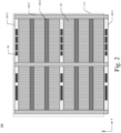
- Fig. 1 is a structure diagram of a semiconductor device provided by some implementations of the present disclosure.
- the semiconductor device 100 may be a wafer, which may be cut to form a plurality of chips, such as a 3D memory.
- the 3D memory may be applied in communication products, consumer electronic products, automobile products, aerospace products, artificial intelligence products or big data, etc.
- Consumer electronic products include, but not limited to mobile phones, computers, tablet computers, cameras, smart glasses or game products, etc.
- a plurality of dies 20 are defined by the intersection of the first cutting lane 11, the second cutting lanes 12 and the third cutting lane 13. That is, the dies 20 are located in regions defined by the intersection of the plurality of cutting lanes 10. For example, one die 20 is disposed in one of the regions.
- the one die 20 referred to herein may include an integrated circuit block defined by the cutting lanes on the wafer but not cut yet.
- the die test structure 30 is only located in the first cutting lane 11, and any one first cutting lane 11 is disposed at least adjacent to one of the second cutting lanes 12. That is, the die test structure 30 is concentrated in the first cutting lane 11 and not disposed in the second cutting lanes 12 and the third cutting lane 13. Also, the second cutting lane 12 is disposed besides each first cutting lane 11. For example, one, two or more of the second cutting lanes 12 are disposed besides each first cutting lane 11. In other words, a cutting lane provided with the die test structure 30 is referred to as the first cutting lane 11, while a cutting lane extending in the same direction of the first cutting lane 11 but not provided with the die test structure 30 is referred to as the second cutting lane 12.
- one, two or more of the second cutting lanes 12 are disposed on one side (the side in the Y direction) of each first cutting lane 11, or the second cutting lanes 12 are disposed on both sides (sides in the Y direction) of each first cutting lane 11 and the numbers of the second cutting lanes 12 on either side may be equal or not equal.
- the first cutting lane 11 and the second cutting lanes 12 may be arranged alternatively such that any one first cutting lane 11 is located between two second cutting lanes 12. That is, the first cutting lane 11 is adjacent to the two second cutting lanes 12. In other words, any one first cutting lane 11 is adjacent to a second cutting lane 12 on either side respectively.
- At least three second cutting lanes 12 may be disposed between adjacent two first cutting lanes 11. As shown in Fig. 1 , any one first cutting lane 11 is disposed adjacent to five second cutting lanes 12 and five second cutting lanes 12 are disposed between adjacent two first cutting lanes 11.
- a plurality of cutting lanes 10 and a plurality of dies 20 may constitute a repeating unit C for mask exposure, which refers to the process of patterning the underlying structure via a mask, including photolithography process.
- the repeating unit C includes at least one first cutting lane 11 and the semiconductor device 100 includes a plurality of the repeating units C.
- Fig. 1 shows one repeating unit C, which implies that the integrated circuit pattern in the semiconductor device 100 is obtained by repeating the repeating unit C in at least one of X direction or Y direction. It is appreciated that a first cutting lane 11 is also provided under the bottom die 20 in Fig. 1 , but the first cutting lane 11 belongs to another repeating unit. It is also appreciated that the first cutting lane 11 at the lower part of Fig. 1 belongs to the repeating unit C while the first cutting lane 11 at the upper part of Fig. 1 belongs to another repeating unit.
- One repeating unit C may be formed by one mask, and 12 dies 20 shown in Fig. 1 may be formed with one mask.
- one repeating unit C may include one first cutting lane 11 and five second cutting lanes 12, and the first cutting lane 11 may be disposed on one side of the five second cutting lanes 12. In other implementations, the first cutting lane 11 may also be between any two second cutting lanes 12. It is to be noted that the numbers of cutting lanes 10 in the present disclosure are only examples, and the numbers of the cutting lanes 10, the first cutting lane 11 and the second cutting lanes 12 are not limited in the present disclosure.
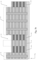
- Fig. 2 is a structure diagram of a semiconductor device provided by some implementations of the present disclosure.
- One repeating unit C1 is shown in the semiconductor device 200 in Fig. 2 , and the repeating unit C1 includes two first cutting lanes 11 and four second cutting lanes 12. That is, in case there are many die test structures 30, the die test structures 30 may be concentrated in the two first cutting lanes 11.
- the die test structures 30 may be concentrated in more than two first cutting lanes 11.
- the number of second cutting lanes 12 spacing between two adjacent first cutting lanes 11 is equal, such that it can guarantee the distribution of die test structures 30 is uniform and the stress may be averaged. For example, there may be two second cutting lanes 12 between two adjacent first cutting lanes 11.
- Fig. 3 is a sectional structure diagram of the semiconductor device in Fig. 1 provided by some implementations of the present disclosure along A-A1.
- the cutting lane 10 may include first dielectric layers 101 and second dielectric layers 102 stacked alternatively, and the die test structure 30 penetrates the cutting lane 10 in the stacking direction (Z) of the cutting lane 10 and may include third dielectric layers 301 and conductive layers 302 stacked alternatively in the stacking direction (Z).
- the materials for the first dielectric layer 101 and the second dielectric layer 102 may include, but not limited to silicon oxide, silicon nitride or silicon oxynitride, and the materials for the first dielectric layer 101 and the second dielectric layer 102 are different.
- the material for the third dielectric layer 301 includes, but not limited to silicon oxide, silicon nitride or silicon oxynitride, of which the example material is silicon oxide.
- the third dielectric layer 301 may have the same material as the first dielectric layer 101 or the second dielectric layer 102.
- both the third dielectric layers 301 and the first dielectric layers 101 are silicon oxide and are disposed on the same layer, and the conductive layer 302 and the second dielectric layer 102 are disposed on the same layer.
- both the third dielectric layer 301 and the second dielectric layer 102 are silicon oxide and disposed on the same layer, and the conductive layer 302 and the first dielectric layer 101 are disposed on the same layer.
- the conductive layer 302 may include one or more conductive materials such as tungsten, titanium carbide, poly-crystalline silicon, etc.
- the conductive layers 302 may further include a high-k material such as aluminum oxide.
- the semiconductor device 100 may further include a semiconductor layer 40 and a stack 50 on the semiconductor layer 40, and the stack 50 includes third dielectric layers 301 and conductive layers 302 stacked alternatively in the stacking direction (Z).
- the cutting lane 10 and the die test structure 30 are located on the semiconductor layer 40.
- a die 20 may include the stack 50 and some channel structures 51, and the die 20 (or the stack 50) is adjacent to the first cutting lane 11 and the second cutting lane 12.
- the thickness of the cutting lane 10 may be equal to the thickness of the stack 50. It is appreciated that the "thickness" in the present disclosure refers to the thickness in Z direction.
- the thickness of the die test structure 30 is smaller than or equal to the thickness of the cutting lane 10.
- the thickness of each of all the die test structures 30 is smaller than the thickness of the cutting lane 10, or the thickness of each of all the die test structures 30 is equal to the thickness of the cutting lane 10.
- the thickness of some die test structures 30 is smaller than the thickness of the cutting lane 10 and the thickness of other die test structures 30 is equal to the thickness of the cutting lane 10.
- the die 20 may further include a memory device and a peripheral circuit (not shown in the figures) bonded with each other.
- the die 20 may be a memory (NAND) grain
- the peripheral circuit may be a CMOS (complementary metal oxide semiconductor).
- the peripheral circuit is electrically connected with the memory device to transfer signals with the memory device.
- the peripheral circuit may be configured to implement logical operations and control and detect on-off states of memory cells in the memory device via metal lines for data storing and reading.
- the die test structure 30 may be configured for electric performance test of the memory device, the peripheral circuit or the bonding interface between the memory device and the peripheral circuit.
- the die test structure 30 may be configured to test electric performance of memory cells in the memory device, test electric performance of transistors in the peripheral circuit, and test electrical connection of the bonding interface.
- Cutting processes may include laser cutting and mechanical cutting.
- the number of conductive layers 302 in the die test structure 30 becomes greater and greater, that is, the thickness of the die test structure 30 becomes greater and greater. If the die test structures 30 are distributed in the first cutting lane 11 and the second cutting lane 12 scatteredly, they may also be distributed in the third cutting lane 13. If only one or two die test structures 30 are disposed in one cutting lane 10, then the cutting lane 10 has different materials at the location with the die test structure 30 and at the location without the die test structure 30. While laser scan cutting is performed along the cutting lane 10, since it is difficult to adjust the output power of the laser in scanning cutting of the same cutting lane 10, different depths are formed by cutting at different locations. In an example, the cutting depth at a location without the die test structure 30 is deeper than the cutting depth at a location with the die test structure 30. A too deep laser cutting depth would result in degraded strength of the device.
- the die test structures 30 are concentrated in the first cutting lane 11 and there is no die test structure 30 in the second cutting lanes 12 and the third cutting lane 13, then it is possible to process the first cutting lane 11 with different laser settings while cutting with laser.
- the laser energy for the second cutting lanes 12 and the third cutting lane 13 is adjusted such that it is smaller than the laser energy for the first cutting lane 11 (even 0), thereby achieving a better consistency of the laser cutting depth for the cutting lanes 10. That is, for the second cutting lanes 12 and the third cutting lane 13 without die test structure 30, it is possible to reduce their laser cutting depth to improve the degradation of the strength of device due to laser cutting. Further, the chip can undergo a greater bending force during the packaging process, thereby reducing the break risk of the chip.
- the die test structures 30 are disposed in the first cutting lane 11 and not disposed at the intersection of the first cutting lane 11 and the third cutting lane 13 such that different cutting conditions may be used for the first cutting lane 11 and the third cutting lane 13 to achieve a better consistency of cutting depth.
- the die test structures 30 with the same thickness in the same first cutting lane 11. For example, the die test structures 30 with a bigger thickness are disposed in one first cutting lane 11, and the die test structures 30 with a smaller thickness are disposed in another first cutting lane 11.
- the laser cutting condition for the first cutting lane 11 in which thinner die test structures 30 are disposed is adjusted such that the laser energy is smaller, which can achieve a better consistency of cutting depth for both of them. It is also possible to reduce the cutting depth of the first cutting lane 11 in which thinner die test structures 30 are disposed to improve the strength of device.
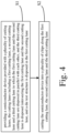
- Fig. 4 is a flow chart of a fabrication method of a chip provided by some implementations of the present disclosure.
- Figs. 5A-5c are structure diagrams of a chip in the fabrication process provided by some implementations of the present disclosure.
- the chip is obtained by cutting the above-described semiconductor device 100, and thus Figs. 1 and 3 may be referred to.
- the fabrication of the chip may include the following operations S1-S2.
- Operation S1 providing a semiconductor device provided with a plurality of cutting lanes 10, the cutting lanes 10 including a first cutting lane 11, a second cutting lane 12 and a third cutting lane 13 in which the first cutting lane 11 and the second cutting lane 12 are disposed in parallel with each other, and the third cutting lane 13 is disposed intersecting the first cutting lane 11 and the second cutting lane 12, and a die test structure 30 is disposed in the first cutting lane 11.
- the die test structures 30 are concentrated in one first cutting lane 11.
- the die 20 is located between two first cutting lanes 11, or between the first cutting lane 11 and the second cutting lane 12.
- Operation S2 cutting the semiconductor device into a plurality of chips 60 along the first cutting lane 11, the second cutting lane 12 and the third cutting lane 13.
- a groove is formed on the front face of the device with laser cutting, and then the semiconductor device is completely cut with a machine such as a blade.
- Laser cutting may make the cutting edge on the front face of device smoother, thereby improving the quality of the front face of the chips 60.
- a first groove 110 in the first cutting lane 11 with a first laser to remove a part of the die test structure 30, wherein the depth of the first groove 110 is smaller than the thickness of the first cutting lane 11.
- the second cutting lane 12, the third cutting lane 13, and the first cutting lane 11 under the first groove 110 are cut mechanically to form a plurality of chips 60.
- the first cutting lane 11 may be cut once with laser to form the groove, while the second cutting lane 12 and the third cutting lane 13 are not cut with laser, and then the first cutting lane 11, the second cutting lane 12 and the third cutting lane 13 are cut mechanically once to cut the semiconductor device into a plurality of chips 60. Therefore, such cutting manner can realize local laser cutting and low-cost high output.
- a second groove 120 in the second cutting lane 12 with a second laser and form a third groove (not shown) in the third cutting lane 13 before performing the described-above mechanical cutting, wherein the depth of the second groove 120 is smaller than the thickness of the second cutting lane 12, and the depth of the third groove is smaller than the thickness of the third cutting lane 13.
- setting the energy of the second laser to be smaller than the energy of the first laser may allow the depth of the second groove 120 and the third groove to be consistent with the depth of the first groove 110. That is, in the case of laser cutting, the laser cutting depth of the second cutting lane 12 and the third cutting lane 13 is reduced to improve the strength of the chips 60.
- the second cutting lane 12 and the third cutting lane 13 are not cut with laser, or the number of burnings with laser is small, it is possible to reduce the laser burning time required for the entire semiconductor device and improve the unit time output.
- the die test structures 30 are concentrated in the first cutting lane 11, it is possible to use different parameters for the first cutting lane 11 than the second cutting lane 12 and the third cutting lane 13 to reduce the laser cutting depth of the second cutting lane 12 and the third cutting lane 13, thereby improving strength of chips 60.
- An implementation of the present disclosure further provides a chip fabricated from the semiconductor device of any one of the above-described implementations.
- the chip includes a first cutting face 61 and a second cutting face 62 outside the first cutting face 61, and the second cutting face 62 has a height in Z direction smaller than the height of the first cutting face 61 in Z direction.
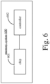
- Fig. 6 is a structure diagram of a memory system provided in some implementations of the present disclosure.
- the memory system 600 includes a chip 601 and a controller 602.
- the chip 601 may be the chip in any of the above-described implementations and may be fabricated from the semiconductor device in the above-described implementations.
- the controller 602 is electrically connected with the chip 601 to control the chip 601 to store data and the chip 601 may execute data storage operations based on the controller's 602 control.
- the memory system may be implemented as multimedia card such as universal flash storage (UFS) device, solid state hard disk (SSD), MMC, eMMC, RS-MMC and mini-MMC, secure digital card such as SD, mini-SD and micro-SD, storage device of Personal Computer Memory Card International Association (PCMCIA) type, storage device of peripheral component interconnect (PCI) type, storage device of PCI Express (PCI-E) type, compact flash (CF) card, smart media card or memory stick etc.
- multimedia card such as universal flash storage (UFS) device, solid state hard disk (SSD), MMC, eMMC, RS-MMC and mini-MMC, secure digital card such as SD, mini-SD and micro-SD
- PCMCIA Personal Computer Memory Card International Association
- PCI peripheral component interconnect
- PCI-E PCI Express
- CF compact flash
Landscapes
- Semiconductor Integrated Circuits (AREA)
- Engineering & Computer Science (AREA)
- Manufacturing & Machinery (AREA)
- Automation & Control Theory (AREA)
- Semiconductor Memories (AREA)
- Dicing (AREA)
Abstract
Description
- The present disclosure generally relates to electronics, and more particularly to a semiconductor device, a chip and a fabrication method thereof, as well as a memory system.
- NAND memory device is a non-volatile memory product with low power consumption, light weight and good performance, which has been widely applied in electronic products. NAND device of planar structure has practically reached its limit in scalability. In order to further increase memory capacity and reduce memory cost per bit, 3D NAND memories are proposed. In a 3D NAND memory architecture, memory cells are arranged in multiple levels stacked vertically to achieve a memory architecture in stack.
- As the stacked layers become more and more, the cutting process of cutting lanes impacts the strength of device more and more.
- The present disclosure aims to provide a semiconductor device and a method of fabricating the same so as to reduce the influence on the strength of device by cutting the cutting lanes.
- In the first aspect, the present disclosure provides a semiconductor device comprising: a plurality of cutting lanes, comprising at least one first cutting lane, a plurality of second cutting lanes and a third cutting lane, wherein the first cutting lane and the second cutting lanes are disposed in parallel with each other, and the third cutting lane is disposed intersecting the first cutting lane and the second cutting lanes; a plurality of dies defined by the intersection of the plurality of cutting lanes; and a die test structure only located in the first cutting lane, wherein any one first cutting lane is disposed at least adjacent to one of the second cutting lanes.
- In some implementations, at least three of the second cutting lanes are arranged between adjacent two of the first cutting lanes.
- In some implementations, a number of the second cutting lanes spaced between the adjacent two of the first cutting lanes is equal.
- In some implementations, the cutting lane comprises first dielectric layers and second dielectric layers stacked alternatively, and the die test structure penetrates the cutting lanes in a stacking direction of the cutting lanes and comprises third dielectric layers and conductive layers stacked alternatively in the stacking direction.
- In some implementations, a thickness of the die test structure is smaller than or equal to a thickness of the cutting lane.
- In some implementations, the die test structures with a same thickness are located in a same first cutting lane.
- In some implementations, the semiconductor device further comprises: a semiconductor layer; a stack on the semiconductor layer and comprising the third dielectric layers and the conductive layers stacked alternatively in the stacking direction; wherein the cutting lane and the die test structure are located on the semiconductor layer.
- In some implementations, the die comprises a memory device and a peripheral circuit bonded with each other, and the die test structure is configured for electric performance test of the memory device, the peripheral circuit or a bonding interface between the memory device and the peripheral circuit.
- In some implementations, the plurality of cutting lanes and the plurality of dies constitute a repeating unit, and the repeating unit comprises at least one first cutting lane and the semiconductor device comprises a plurality of the repeating units.
- In the second aspect, the present disclosure provides a chip fabricated from the semiconductor device in any one of the above-described implementations, the chip comprising a first cutting face and a second cutting face outside the first cutting face, and the second cutting face has a height smaller than a height of the first cutting face.
- In the third aspect, the present disclosure provides a memory system comprising: the chip provided in the above-described implementations; and a controller electrically connected with the chip to control the chip to store data.
- In the fourth aspect, the present disclosure provides a fabrication method of a chip comprising: providing a semiconductor device provided with a plurality of cutting lanes, the cutting lanes comprising a first cutting lane, a second cutting lane and a third cutting lane, wherein the first cutting lane and the second cutting lane are disposed in parallel with each other, and the third cutting lane is disposed intersecting the first cutting lane and the second cutting lane, and a die test structure is disposed in the first cutting lane; and cutting the semiconductor device into a plurality of chips along the first cutting lane, the second cutting lane and the third cutting lane.
- In some implementations, the cutting the semiconductor device into the plurality of chips along the first cutting lane, the second cutting lane and the third cutting lane comprises: cutting the semiconductor device twice with two different cutting processes, respectively.
- In some implementations, the cutting the semiconductor device into a plurality of chips along the first cutting lane, the second cutting lane and the third cutting lane comprises: forming a first groove in the first cutting lane with a first laser to remove a part of the die test structure, wherein a depth of the first groove is smaller than a thickness of the first cutting lane; and cutting mechanically the second cutting lane, the third cutting lane, and the first cutting lane under the first groove to form the plurality of chips.
- In some implementations, before cutting the first cutting lane under the first groove, the second cutting lane and the third cutting lane with a blade, the fabrication method of the chip further comprises: forming a second groove in the second cutting lane and forming a third groove in the third cutting lane with a second laser, wherein a depth of the second groove is smaller than a thickness of the second cutting lane, and a depth of the third groove is smaller than a thickness of the third cutting lane; the cutting mechanically the second cutting lane, the third cutting lane and the first cutting lane under the first groove comprises: cutting the first cutting lane under the first groove, the second cutting lane under the second groove and the third cutting lane under the third groove with the blade.
- In some implementations, an energy of the second laser is smaller than an energy of the first laser.
- The present disclosure provides a semiconductor device, a chip and a fabrication method thereof, as well as a memory system. The semiconductor device includes a plurality of cutting lanes, a plurality of dies and a die test structure, and the plurality of dies are defined by the intersection of the plurality of cutting lanes. The plurality of cutting lanes include at least one first cutting lane, a plurality of second cutting lanes and a third cutting lane, wherein the first cutting lane and the second cutting lanes are disposed in parallel with each other, and the third cutting lane is disposed intersecting the first cutting lane and the second cutting lanes. The die test structure is only located in the first cutting lane, and any one first cutting lane is disposed at least adjacent to one of the second cutting lanes. By concentrating the die test structure in the first cutting lane rather than in the second cutting lane and the third cutting lane, it is possible to use different laser cutting conditions for the cutting lane with the die test structure and the cutting lane without the die test structure while performing cutting process such that the laser cutting depth of the second cutting lane and the third cutting lane is reduced, thereby improving the strength of the device.
- Technical solutions and other beneficial effects of the present disclosure will become apparent from the following detailed description of implementations of the present disclosure in connection with the accompanying drawings.
-
Fig. 1 is a structure diagram of a semiconductor device provided by some implementations of the present disclosure; -
Fig. 2 is a structure diagram of a semiconductor device provided by some implementations of the present disclosure; -
Fig. 3 is a sectional structure diagram of a semiconductor device inFig. 1 provided by some implementations of the present disclosure along A-A1; -
Fig. 4 is a flow chart of a fabrication method of a chip provided by some implementations of the present disclosure; -
Figs. 5a-5c are structure diagrams of a chip in the fabrication process provided by some implementations of the present disclosure; and -
Fig. 6 is a structure diagram of a memory system provided by some implementations of the present disclosure. - The technical solutions in implementations of the present disclosure will be described clearly and fully below in connection with accompanying drawings in implementations of the present disclosure. Obviously, the described implementations are only a part of implementations of the present disclosure rather than all of them. All other implementations obtained by those skilled in the art based on the implementations of the present disclosure without any creative works fall within the scope of the present disclosure.
- It should be understood that terms "first", "second" etc. may be used to describe various components herein, but are not intended to limit them. These terms are only used to partition one component from another. For example, a "first component" may be referred to as a "second component" and likewise a "second component" may be referred to as a "first component" without departing from the scope of the present disclosure.
- It should be understood that when a component is described to be "on" or "connected to" another component, it can be directly on or connected to the another component or there may be intervening components. Other terms for describing relationship among components should be interpreted similarly.
- As used herein, the term "layer" refers to a part of material including a region with a thickness. A layer can extend over the entirety of an underlying or overlying structure or may have an extent less than the extent of an underlying or overlying structure. Furthermore, a layer may be a region of uniform or non-uniform continuous structure with a thickness smaller than that of a continuous structure. For example, a layer may be between the top surface and bottom surface of a continuous structure or between any group of horizontal planes at the top surface and the bottom surface. A layer may extend horizontally, vertically and/or along a conical surface. The substrate may be a layer that may include one or more layers therein and/or may have one or more layers on, over and/or under it. A layer can include multiple layers. For example, an interconnect layer can include one or more conductive layers and contact layers (in which contacts, interconnect lines and/or vertical interconnect accesses (VIA) are formed) and one or more dielectric layers.
- It is to be noted that the drawings provided in the implementations of the present disclosure only illustrates the basic conception of the present disclosure schematically. Although only the components related to this disclosure are shown in the drawing, and not drawn according to the number, shape and size of components in actual implementation, the type, number and proportion of components in actual implementation can be changed at will, and the layout of components may be more complicated.
- Referring to
Fig. 1, Fig. 1 is a structure diagram of a semiconductor device provided by some implementations of the present disclosure. Thesemiconductor device 100 may be a wafer, which may be cut to form a plurality of chips, such as a 3D memory. The 3D memory may be applied in communication products, consumer electronic products, automobile products, aerospace products, artificial intelligence products or big data, etc. Consumer electronic products include, but not limited to mobile phones, computers, tablet computers, cameras, smart glasses or game products, etc. - The
semiconductor device 100 includes a plurality of cutting lanes 10, a plurality ofdies 20 and adie test structure 30, in which the plurality ofdies 20 are defined by the intersection of the plurality of cutting lanes 10. The plurality of cutting lanes 10 include at least one first cutting lane 11, a plurality of second cutting lanes 12 and a third cutting lane 13 in which the first cutting lane 11 and the second cutting lanes 12 are disposed in parallel with each other, and the third cutting lane 13 is disposed intersecting the first cutting lane 11 and the second cutting lanes 12. For example, both the first cutting lane 11 and the second cutting lanes 12 may be disposed in the X direction, and the third cutting lane 13 may be disposed in the Y direction. A plurality of dies 20 are defined by the intersection of the first cutting lane 11, the second cutting lanes 12 and the third cutting lane 13. That is, the dies 20 are located in regions defined by the intersection of the plurality of cutting lanes 10. For example, one die 20 is disposed in one of the regions. The one die 20 referred to herein may include an integrated circuit block defined by the cutting lanes on the wafer but not cut yet. - The
die test structure 30 is only located in the first cutting lane 11, and any one first cutting lane 11 is disposed at least adjacent to one of the second cutting lanes 12. That is, thedie test structure 30 is concentrated in the first cutting lane 11 and not disposed in the second cutting lanes 12 and the third cutting lane 13. Also, the second cutting lane 12 is disposed besides each first cutting lane 11. For example, one, two or more of the second cutting lanes 12 are disposed besides each first cutting lane 11. In other words, a cutting lane provided with thedie test structure 30 is referred to as the first cutting lane 11, while a cutting lane extending in the same direction of the first cutting lane 11 but not provided with thedie test structure 30 is referred to as the second cutting lane 12. In an example, one, two or more of the second cutting lanes 12 are disposed on one side (the side in the Y direction) of each first cutting lane 11, or the second cutting lanes 12 are disposed on both sides (sides in the Y direction) of each first cutting lane 11 and the numbers of the second cutting lanes 12 on either side may be equal or not equal. - In some implementations, the first cutting lane 11 and the second cutting lanes 12 may be arranged alternatively such that any one first cutting lane 11 is located between two second cutting lanes 12. That is, the first cutting lane 11 is adjacent to the two second cutting lanes 12. In other words, any one first cutting lane 11 is adjacent to a second cutting lane 12 on either side respectively.
- In some implementations, at least three second cutting lanes 12 may be disposed between adjacent two first cutting lanes 11. As shown in
Fig. 1 , any one first cutting lane 11 is disposed adjacent to five second cutting lanes 12 and five second cutting lanes 12 are disposed between adjacent two first cutting lanes 11. - In some implementations, a plurality of cutting lanes 10 and a plurality of dies 20 may constitute a repeating unit C for mask exposure, which refers to the process of patterning the underlying structure via a mask, including photolithography process. The repeating unit C includes at least one first cutting lane 11 and the
semiconductor device 100 includes a plurality of the repeating units C. -
Fig. 1 shows one repeating unit C, which implies that the integrated circuit pattern in thesemiconductor device 100 is obtained by repeating the repeating unit C in at least one of X direction or Y direction. It is appreciated that a first cutting lane 11 is also provided under the bottom die 20 inFig. 1 , but the first cutting lane 11 belongs to another repeating unit. It is also appreciated that the first cutting lane 11 at the lower part ofFig. 1 belongs to the repeating unit C while the first cutting lane 11 at the upper part ofFig. 1 belongs to another repeating unit. One repeating unit C may be formed by one mask, and 12 dies 20 shown inFig. 1 may be formed with one mask. - As shown in
Fig. 1 , one repeating unit C may include one first cutting lane 11 and five second cutting lanes 12, and the first cutting lane 11 may be disposed on one side of the five second cutting lanes 12. In other implementations, the first cutting lane 11 may also be between any two second cutting lanes 12. It is to be noted that the numbers of cutting lanes 10 in the present disclosure are only examples, and the numbers of the cutting lanes 10, the first cutting lane 11 and the second cutting lanes 12 are not limited in the present disclosure. - Referring to
Fig. 2, Fig. 2 is a structure diagram of a semiconductor device provided by some implementations of the present disclosure. One repeating unit C1 is shown in thesemiconductor device 200 inFig. 2 , and the repeating unit C1 includes two first cutting lanes 11 and four second cutting lanes 12. That is, in case there are many dietest structures 30, thedie test structures 30 may be concentrated in the two first cutting lanes 11. - In some implementations, in case there are many die
test structures 30, thedie test structures 30 may be concentrated in more than two first cutting lanes 11. - In some implementations, the number of second cutting lanes 12 spacing between two adjacent first cutting lanes 11 is equal, such that it can guarantee the distribution of
die test structures 30 is uniform and the stress may be averaged. For example, there may be two second cutting lanes 12 between two adjacent first cutting lanes 11. - Referring to
Fig. 3, Fig. 3 is a sectional structure diagram of the semiconductor device inFig. 1 provided by some implementations of the present disclosure along A-A1. - The cutting lane 10 may include first
dielectric layers 101 and seconddielectric layers 102 stacked alternatively, and thedie test structure 30 penetrates the cutting lane 10 in the stacking direction (Z) of the cutting lane 10 and may include thirddielectric layers 301 andconductive layers 302 stacked alternatively in the stacking direction (Z). - The materials for the
first dielectric layer 101 and thesecond dielectric layer 102 may include, but not limited to silicon oxide, silicon nitride or silicon oxynitride, and the materials for thefirst dielectric layer 101 and thesecond dielectric layer 102 are different. The material for the thirddielectric layer 301 includes, but not limited to silicon oxide, silicon nitride or silicon oxynitride, of which the example material is silicon oxide. The thirddielectric layer 301 may have the same material as thefirst dielectric layer 101 or thesecond dielectric layer 102. For example, both the thirddielectric layers 301 and the firstdielectric layers 101 are silicon oxide and are disposed on the same layer, and theconductive layer 302 and thesecond dielectric layer 102 are disposed on the same layer. Alternatively, both the thirddielectric layer 301 and thesecond dielectric layer 102 are silicon oxide and disposed on the same layer, and theconductive layer 302 and thefirst dielectric layer 101 are disposed on the same layer. - The
conductive layer 302 may include one or more conductive materials such as tungsten, titanium carbide, poly-crystalline silicon, etc. Theconductive layers 302 may further include a high-k material such as aluminum oxide. - The
semiconductor device 100 may further include asemiconductor layer 40 and astack 50 on thesemiconductor layer 40, and thestack 50 includes thirddielectric layers 301 andconductive layers 302 stacked alternatively in the stacking direction (Z). The cutting lane 10 and thedie test structure 30 are located on thesemiconductor layer 40. A die 20 may include thestack 50 and somechannel structures 51, and the die 20 (or the stack 50) is adjacent to the first cutting lane 11 and the second cutting lane 12. - In some implementations, the thickness of the cutting lane 10 may be equal to the thickness of the
stack 50. It is appreciated that the "thickness" in the present disclosure refers to the thickness in Z direction. - In some implementations, the thickness of the
die test structure 30 is smaller than or equal to the thickness of the cutting lane 10. - In some implementations, the thickness of each of all the
die test structures 30 is smaller than the thickness of the cutting lane 10, or the thickness of each of all thedie test structures 30 is equal to the thickness of the cutting lane 10. - In some implementations, the thickness of some die
test structures 30 is smaller than the thickness of the cutting lane 10 and the thickness of otherdie test structures 30 is equal to the thickness of the cutting lane 10. - The die 20 may further include a memory device and a peripheral circuit (not shown in the figures) bonded with each other. Herein, the
die 20 may be a memory (NAND) grain, and the peripheral circuit may be a CMOS (complementary metal oxide semiconductor). The peripheral circuit is electrically connected with the memory device to transfer signals with the memory device. The peripheral circuit may be configured to implement logical operations and control and detect on-off states of memory cells in the memory device via metal lines for data storing and reading. - The
die test structure 30 may be configured for electric performance test of the memory device, the peripheral circuit or the bonding interface between the memory device and the peripheral circuit. For example, thedie test structure 30 may be configured to test electric performance of memory cells in the memory device, test electric performance of transistors in the peripheral circuit, and test electrical connection of the bonding interface. - In some implementations, it is possible to separate the plurality of dies 20 to obtain a plurality of chips by cutting the
semiconductor device 100 along the first cutting lane 11, the second cutting lanes 12 and the third cutting lane 13. Cutting processes may include laser cutting and mechanical cutting. - As found by the inventor through study, as the layers of the
stack 50 become more and more, the number ofconductive layers 302 in thedie test structure 30 becomes greater and greater, that is, the thickness of thedie test structure 30 becomes greater and greater. If thedie test structures 30 are distributed in the first cutting lane 11 and the second cutting lane 12 scatteredly, they may also be distributed in the third cutting lane 13. If only one or two dietest structures 30 are disposed in one cutting lane 10, then the cutting lane 10 has different materials at the location with thedie test structure 30 and at the location without thedie test structure 30. While laser scan cutting is performed along the cutting lane 10, since it is difficult to adjust the output power of the laser in scanning cutting of the same cutting lane 10, different depths are formed by cutting at different locations. In an example, the cutting depth at a location without thedie test structure 30 is deeper than the cutting depth at a location with thedie test structure 30. A too deep laser cutting depth would result in degraded strength of the device. - In the semiconductor device provided by implementations of the present disclosure, the
die test structures 30 are concentrated in the first cutting lane 11 and there is nodie test structure 30 in the second cutting lanes 12 and the third cutting lane 13, then it is possible to process the first cutting lane 11 with different laser settings while cutting with laser. For example, the laser energy for the second cutting lanes 12 and the third cutting lane 13 is adjusted such that it is smaller than the laser energy for the first cutting lane 11 (even 0), thereby achieving a better consistency of the laser cutting depth for the cutting lanes 10. That is, for the second cutting lanes 12 and the third cutting lane 13 withoutdie test structure 30, it is possible to reduce their laser cutting depth to improve the degradation of the strength of device due to laser cutting. Further, the chip can undergo a greater bending force during the packaging process, thereby reducing the break risk of the chip. - In some implementations, the
die test structures 30 are disposed in the first cutting lane 11 and not disposed at the intersection of the first cutting lane 11 and the third cutting lane 13 such that different cutting conditions may be used for the first cutting lane 11 and the third cutting lane 13 to achieve a better consistency of cutting depth. - In some implementations, it is possible to dispose the
die test structures 30 with the same thickness in the same first cutting lane 11. For example, thedie test structures 30 with a bigger thickness are disposed in one first cutting lane 11, and thedie test structures 30 with a smaller thickness are disposed in another first cutting lane 11. - As compared to the first cutting lane 11 in which thicker
die test structures 30 are disposed, the laser cutting condition for the first cutting lane 11 in which thinnerdie test structures 30 are disposed is adjusted such that the laser energy is smaller, which can achieve a better consistency of cutting depth for both of them. It is also possible to reduce the cutting depth of the first cutting lane 11 in which thinnerdie test structures 30 are disposed to improve the strength of device. - Referring to
Fig. 4, Fig. 4 is a flow chart of a fabrication method of a chip provided by some implementations of the present disclosure. Referring toFigs. 5A-5c at the same time,Figs. 5a-5c are structure diagrams of a chip in the fabrication process provided by some implementations of the present disclosure. The chip is obtained by cutting the above-describedsemiconductor device 100, and thusFigs. 1 and3 may be referred to. The fabrication of the chip may include the following operations S1-S2. - Operation S1: providing a semiconductor device provided with a plurality of cutting lanes 10, the cutting lanes 10 including a first cutting lane 11, a second cutting lane 12 and a third cutting lane 13 in which the first cutting lane 11 and the second cutting lane 12 are disposed in parallel with each other, and the third cutting lane 13 is disposed intersecting the first cutting lane 11 and the second cutting lane 12, and a
die test structure 30 is disposed in the first cutting lane 11. - For example, referring to
Fig. 1 , in one repeating unit C, thedie test structures 30 are concentrated in one first cutting lane 11. As shown inFig. 5a , thedie 20 is located between two first cutting lanes 11, or between the first cutting lane 11 and the second cutting lane 12. - Operation S2: cutting the semiconductor device into a plurality of
chips 60 along the first cutting lane 11, the second cutting lane 12 and the third cutting lane 13. - In some implementations, it is possible to cut the semiconductor device twice with two different cutting processes. For example, a groove is formed on the front face of the device with laser cutting, and then the semiconductor device is completely cut with a machine such as a blade. Laser cutting may make the cutting edge on the front face of device smoother, thereby improving the quality of the front face of the
chips 60. - As shown in
Fig. 5b , it is possible to form afirst groove 110 in the first cutting lane 11 with a first laser to remove a part of thedie test structure 30, wherein the depth of thefirst groove 110 is smaller than the thickness of the first cutting lane 11. As shown inFig. 5c , then the second cutting lane 12, the third cutting lane 13, and the first cutting lane 11 under thefirst groove 110 are cut mechanically to form a plurality ofchips 60. That is, the first cutting lane 11 may be cut once with laser to form the groove, while the second cutting lane 12 and the third cutting lane 13 are not cut with laser, and then the first cutting lane 11, the second cutting lane 12 and the third cutting lane 13 are cut mechanically once to cut the semiconductor device into a plurality ofchips 60. Therefore, such cutting manner can realize local laser cutting and low-cost high output. - In some implementations, it is also possible to form a
second groove 120 in the second cutting lane 12 with a second laser and form a third groove (not shown) in the third cutting lane 13 before performing the described-above mechanical cutting, wherein the depth of thesecond groove 120 is smaller than the thickness of the second cutting lane 12, and the depth of the third groove is smaller than the thickness of the third cutting lane 13. - Since there is no the
die test structure 30 in the second cutting lane 12 and the third cutting lane 13, setting the energy of the second laser to be smaller than the energy of the first laser may allow the depth of thesecond groove 120 and the third groove to be consistent with the depth of thefirst groove 110. That is, in the case of laser cutting, the laser cutting depth of the second cutting lane 12 and the third cutting lane 13 is reduced to improve the strength of thechips 60. - In some implementations, it is also possible to reduce the number of burnings with the second laser (smaller than the number of burnings with the first laser) such that the depth of the
second groove 120 and the third groove to be consistent with the depth of thefirst groove 110. In case that the second cutting lane 12 and the third cutting lane 13 are not cut with laser, or the number of burnings with laser is small, it is possible to reduce the laser burning time required for the entire semiconductor device and improve the unit time output. - It is appreciated that as shown in
Fig. 1 , since thedie test structures 30 do not cover the first cutting lane 11 completely, there are intervals between thedie test structures 30, therefore the cutting depth in thedie test structures 30 will be smaller than the laser cutting depth at the intervals while cutting the first cutting lane 11 with laser scanning. - With the fabrication method of chips provided by implementations of the present disclosure, since the
die test structures 30 are concentrated in the first cutting lane 11, it is possible to use different parameters for the first cutting lane 11 than the second cutting lane 12 and the third cutting lane 13 to reduce the laser cutting depth of the second cutting lane 12 and the third cutting lane 13, thereby improving strength ofchips 60. - An implementation of the present disclosure further provides a chip fabricated from the semiconductor device of any one of the above-described implementations. Referring to
Fig. 5c , the chip includes afirst cutting face 61 and asecond cutting face 62 outside thefirst cutting face 61, and thesecond cutting face 62 has a height in Z direction smaller than the height of thefirst cutting face 61 in Z direction. - Referring to
Fig. 6, Fig. 6 is a structure diagram of a memory system provided in some implementations of the present disclosure. Thememory system 600 includes achip 601 and acontroller 602. Thechip 601 may be the chip in any of the above-described implementations and may be fabricated from the semiconductor device in the above-described implementations. Thecontroller 602 is electrically connected with thechip 601 to control thechip 601 to store data and thechip 601 may execute data storage operations based on the controller's 602 control. - In some implementations, the memory system may be implemented as multimedia card such as universal flash storage (UFS) device, solid state hard disk (SSD), MMC, eMMC, RS-MMC and mini-MMC, secure digital card such as SD, mini-SD and micro-SD, storage device of Personal Computer Memory Card International Association (PCMCIA) type, storage device of peripheral component interconnect (PCI) type, storage device of PCI Express (PCI-E) type, compact flash (CF) card, smart media card or memory stick etc.
- Description of the implementations above is only used to facilitate understanding of the technical solutions and the core concept of the present disclosure. It can be understood by those of ordinary skills in the art that the technical solutions described in the foregoing various implementations can be modified or have some technical features therein replaced equivalently without departing from the spirit and scope of the technical solutions in the implementations of the present disclosure.
Claims (16)
- A semiconductor device comprising:a plurality of cutting lanes, comprising at least one first cutting lane, a plurality of second cutting lanes and a third cutting lane, wherein the first cutting lane and the second cutting lanes are disposed in parallel with each other, and the third cutting lane is disposed intersecting the first cutting lane and the second cutting lanes;a plurality of dies defined by the intersection of the plurality of cutting lanes; anda die test structure only located in the first cutting lane, wherein any one first cutting lane is disposed at least adjacent to one of the second cutting lanes.
- The semiconductor device of claim 1, wherein at least three of the second cutting lanes are arranged between adjacent two of the first cutting lanes.
- The semiconductor device of claim 1, wherein a number of the second cutting lanes spaced between the adjacent two of the first cutting lanes is equal.
- The semiconductor device of claim 1, wherein the cutting lane comprises first dielectric layers and second dielectric layers stacked alternatively, and the die test structure penetrates the cutting lanes in a stacking direction of the cutting lanes and comprises third dielectric layers and conductive layers stacked alternatively in the stacking direction.
- The semiconductor device of claim 4, wherein a thickness of the die test structure is smaller than or equal to a thickness of the cutting lane.
- The semiconductor device of claim 5, wherein the die test structures with a same thickness are located in the same first cutting lane.
- The semiconductor device of claim 4, further comprising:a semiconductor layer;a stack on the semiconductor layer and comprising the third dielectric layers and the conductive layers stacked alternatively in the stacking direction;wherein the cutting lanes and the die test structure are located on the semiconductor layer.
- The semiconductor device of claim 1, wherein the die comprises a memory device and a peripheral circuit bonded with each other, and the die test structure is configured for electric performance test of the memory device, the peripheral circuit or a bonding interface between the memory device and the peripheral circuit.
- The semiconductor device of claim 1, wherein the plurality of cutting lanes and the plurality of dies constitute a repeating unit, and the repeating unit comprises the at least one first cutting lane and the semiconductor device comprises a plurality of the repeating units.
- A chip fabricated from the semiconductor device of any one of claims 1-9, wherein the chip comprises a first cutting face and a second cutting face outside the first cutting face, and the second cutting face has a height smaller than a height of the first cutting face.
- A memory system comprising:the chip of claim 10; anda controller electrically connected with the chip to control the chip to store data.
- A fabrication method of a chip, comprising:providing a semiconductor device provided with a plurality of cutting lanes, the cutting lanes comprising a first cutting lane, a second cutting lane and a third cutting lane, wherein the first cutting lane and the second cutting lane are disposed in parallel with each other, and the third cutting lane is disposed intersecting the first cutting lane and the second cutting lane, and a die test structure is disposed in the first cutting lane; andcutting the semiconductor device into a plurality of chips along the first cutting lane, the second cutting lane and the third cutting lane.
- The fabrication method of the chip of claim 12, wherein the cutting the semiconductor device into a plurality of chips along the first cutting lane, the second cutting lane and the third cutting lane comprises:
cutting the semiconductor device twice with two different cutting processes, respectively. - The fabrication method of the chip of claim 13, wherein the cutting the semiconductor device into a plurality of chips along the first cutting lane, the second cutting lane and the third cutting lane comprises:forming a first groove in the first cutting lane with a first laser to remove a part of the die test structure, wherein a depth of the first groove is smaller than a thickness of the first cutting lane; andcutting mechanically the second cutting lane, the third cutting lane and the first cutting lane under the first groove to form a plurality of chips.
- The fabrication method of the chip of claim 14, wherein before cutting the first cutting lane under the first groove, the second cutting lane and the third cutting lane with a blade, the fabrication method of the chip further comprises:forming a second groove in the second cutting lane and forming a third groove in the third cutting lane with a second laser, wherein a depth of the second groove is smaller than a thickness of the second cutting lane, and a depth of the third groove is smaller than a thickness of the third cutting lane;the cutting mechanically the second cutting lane, the third cutting lane and the first cutting lane under the first groove comprises: cutting the first cutting lane under the first groove, the second cutting lane under the second groove and the third cutting lane under the third groove with the blade.
- The fabrication method of the chip of claim 15, wherein an energy of the second laser is smaller than an energy of the first laser.
Applications Claiming Priority (1)
| Application Number | Priority Date | Filing Date | Title |
|---|---|---|---|
| PCT/CN2023/111492 WO2025030318A1 (en) | 2023-08-07 | 2023-08-07 | Semiconductor device, chip and preparation method therefor, and storage system |
Publications (2)
| Publication Number | Publication Date |
|---|---|
| EP4531515A1 true EP4531515A1 (en) | 2025-04-02 |
| EP4531515A4 EP4531515A4 (en) | 2025-10-29 |
Family
ID=94481249
Family Applications (1)
| Application Number | Title | Priority Date | Filing Date |
|---|---|---|---|
| EP23925596.1A Pending EP4531515A4 (en) | 2023-08-07 | 2023-08-07 | Semiconductor component, chip and manufacturing process therefor, as well as storage system |
Country Status (6)
| Country | Link |
|---|---|
| US (1) | US20250054905A1 (en) |
| EP (1) | EP4531515A4 (en) |
| KR (1) | KR20250022652A (en) |
| CN (1) | CN119895572A (en) |
| TW (1) | TWI905835B (en) |
| WO (1) | WO2025030318A1 (en) |
Family Cites Families (12)
| Publication number | Priority date | Publication date | Assignee | Title |
|---|---|---|---|---|
| US6967111B1 (en) * | 2003-08-28 | 2005-11-22 | Altera Corporation | Techniques for reticle layout to modify wafer test structure area |
| US8519512B2 (en) * | 2006-09-22 | 2013-08-27 | Taiwan Semiconductor Manufacturing Company, Ltd. | Test line placement to improve die sawing quality |
| US8952497B2 (en) * | 2012-09-14 | 2015-02-10 | Taiwan Semiconductor Manufacturing Company, Ltd. | Scribe lines in wafers |
| US9431288B2 (en) * | 2013-09-18 | 2016-08-30 | Taiwan Semiconductor Manufacturing Company, Ltd. | System and method for test key characterizing wafer processing state |
| KR102677081B1 (en) * | 2016-12-28 | 2024-06-21 | 삼성전자주식회사 | Scribe lane structure including via hole of pad arranged in sawing line |
| CN107146772A (en) * | 2017-03-30 | 2017-09-08 | 北京时代民芯科技有限公司 | It is a kind of to reduce the cutting method that resolution chart influences on scribing quality |
| KR102542621B1 (en) * | 2018-08-17 | 2023-06-15 | 삼성전자주식회사 | Semiconductor device |
| TW202034485A (en) * | 2019-03-08 | 2020-09-16 | 力成科技股份有限公司 | Fan out package structure with plural integrated circuit units and manufacturing method thereof |
| CN110265475A (en) * | 2019-06-24 | 2019-09-20 | 长江存储科技有限责任公司 | A kind of wafer and its manufacturing method, wafer dividing method |
| KR102795466B1 (en) * | 2019-12-10 | 2025-04-15 | 삼성전자주식회사 | Semiconductor devices including a scribe lane and method of forming the same |
| CN114815341A (en) * | 2021-01-21 | 2022-07-29 | 深圳晶微峰光电科技有限公司 | Silicon-based liquid crystal panel and preparation method thereof |
| US20230014850A1 (en) * | 2021-07-15 | 2023-01-19 | Xiamen San'an Optoelectronics Co., Ltd. | Flip-chip light-emitting diode and semiconductor light-emitting device |
-
2023
- 2023-08-07 CN CN202380010049.2A patent/CN119895572A/en active Pending
- 2023-08-07 WO PCT/CN2023/111492 patent/WO2025030318A1/en active Pending
- 2023-08-07 KR KR1020247029576A patent/KR20250022652A/en active Pending
- 2023-08-07 EP EP23925596.1A patent/EP4531515A4/en active Pending
- 2023-12-06 US US18/531,542 patent/US20250054905A1/en active Pending
-
2024
- 2024-07-08 TW TW113125457A patent/TWI905835B/en active
Also Published As
| Publication number | Publication date |
|---|---|
| WO2025030318A1 (en) | 2025-02-13 |
| US20250054905A1 (en) | 2025-02-13 |
| TW202508422A (en) | 2025-02-16 |
| TWI905835B (en) | 2025-11-21 |
| KR20250022652A (en) | 2025-02-17 |
| EP4531515A4 (en) | 2025-10-29 |
| CN119895572A (en) | 2025-04-25 |
Similar Documents
| Publication | Publication Date | Title |
|---|---|---|
| DE112012006625T5 (en) | Multi-chip semiconductor structure with vertical intermediate side chip and semiconductor package therefor | |
| DE102011054908A1 (en) | Semiconductor device, manufacturing method thereof and semiconductor package with this semiconductor device | |
| US20240321777A1 (en) | Methods for forming three-dimensional memory devices | |
| US20250293175A1 (en) | Three dimensional (3d) memory device and fabrication method | |
| US20260089941A1 (en) | Semiconductor device, memory device, and memory system | |
| EP4531515A1 (en) | Semiconductor device, chip and preparation method therefor, and storage system | |
| DE112016005795T5 (en) | INTEGRATED CIRCUIT ARRANGEMENT WITH STACKED RAW CHIPS | |
| US20250056799A1 (en) | Semiconductor memory device, and semiconductor package and electronic system including the same | |
| TW202610408A (en) | Semiconductor device, chip and manufacturing method thereof, and storage system | |
| CN220121247U (en) | Storage systems and electronic equipment | |
| US20240379369A1 (en) | Semiconductor device and method of forming thereof | |
| CN114093882A (en) | Preparation method, semiconductor structure, memory, system and electronic equipment | |
| US12432923B2 (en) | Memory device and fabrication method thereof | |
| US12520488B2 (en) | Three-dimensional memory device and fabrication method for improved yield and reliability | |
| US20240292614A1 (en) | Memory semiconductor device and fabrication method thereof | |
| CN112385038A (en) | Novel 3D cross-point memory structures formed by XTACKING to improve memory array efficiency and enable scaling | |
| US20240215237A1 (en) | Three dimensional (3d) memory device and fabrication method | |
| CN117693206A (en) | Semiconductor device, manufacturing method thereof, memory and memory system | |
| CN119072131A (en) | A semiconductor device and its manufacturing method, memory and storage system | |
| US20250062284A1 (en) | Thin wafer, method of manufacturing the thin wafer, stack type semiconductor device including the thin wafer and method of manufacturing the stack type semiconductor device | |
| CN119730241B (en) | A semiconductor device and its fabrication method, a memory and a storage system | |
| CN113261086B (en) | Method for manufacturing three-dimensional semiconductor device using buried stop layer in substrate | |
| TWI895673B (en) | Three-dimensional memory device and method of forming same | |
| CN119072130A (en) | A semiconductor device and its manufacturing method, memory and storage system | |
| US20240098989A1 (en) | Three-dimensional memory devices and methods for forming the same |
Legal Events
| Date | Code | Title | Description |
|---|---|---|---|
| STAA | Information on the status of an ep patent application or granted ep patent |
Free format text: STATUS: UNKNOWN |
|
| STAA | Information on the status of an ep patent application or granted ep patent |
Free format text: STATUS: THE INTERNATIONAL PUBLICATION HAS BEEN MADE |
|
| PUAI | Public reference made under article 153(3) epc to a published international application that has entered the european phase |
Free format text: ORIGINAL CODE: 0009012 |
|
| STAA | Information on the status of an ep patent application or granted ep patent |
Free format text: STATUS: REQUEST FOR EXAMINATION WAS MADE |
|
| 17P | Request for examination filed |
Effective date: 20240911 |
|
| AK | Designated contracting states |
Kind code of ref document: A1 Designated state(s): AL AT BE BG CH CY CZ DE DK EE ES FI FR GB GR HR HU IE IS IT LI LT LU LV MC ME MK MT NL NO PL PT RO RS SE SI SK SM TR |
|
| REG | Reference to a national code |
Ref country code: DE Ref legal event code: R079 Free format text: PREVIOUS MAIN CLASS: H10B0080000000 Ipc: H01L0021660000 |
|
| RIC1 | Information provided on ipc code assigned before grant |
Ipc: H01L 21/66 20060101AFI20250703BHEP Ipc: H01L 23/00 20060101ALI20250703BHEP Ipc: H10B 43/27 20230101ALI20250703BHEP Ipc: H10B 80/00 20230101ALI20250703BHEP |
|
| A4 | Supplementary search report drawn up and despatched |
Effective date: 20251001 |
|
| RIC1 | Information provided on ipc code assigned before grant |
Ipc: H01L 21/66 20060101AFI20250925BHEP Ipc: H01L 23/00 20060101ALI20250925BHEP Ipc: H10B 43/27 20230101ALI20250925BHEP Ipc: H10B 80/00 20230101ALI20250925BHEP |