EP4531501A1 - Flexible wiring board unit and dimmer unit - Google Patents
Flexible wiring board unit and dimmer unit Download PDFInfo
- Publication number
- EP4531501A1 EP4531501A1 EP23811751.9A EP23811751A EP4531501A1 EP 4531501 A1 EP4531501 A1 EP 4531501A1 EP 23811751 A EP23811751 A EP 23811751A EP 4531501 A1 EP4531501 A1 EP 4531501A1
- Authority
- EP
- European Patent Office
- Prior art keywords
- wiring board
- flexible wiring
- terminal
- relay terminal
- terminals
- Prior art date
- Legal status (The legal status is an assumption and is not a legal conclusion. Google has not performed a legal analysis and makes no representation as to the accuracy of the status listed.)
- Pending
Links
Images









Classifications
-
- G—PHYSICS
- G02—OPTICS
- G02F—OPTICAL DEVICES OR ARRANGEMENTS FOR THE CONTROL OF LIGHT BY MODIFICATION OF THE OPTICAL PROPERTIES OF THE MEDIA OF THE ELEMENTS INVOLVED THEREIN; NON-LINEAR OPTICS; FREQUENCY-CHANGING OF LIGHT; OPTICAL LOGIC ELEMENTS; OPTICAL ANALOGUE/DIGITAL CONVERTERS
- G02F1/00—Devices or arrangements for the control of the intensity, colour, phase, polarisation or direction of light arriving from an independent light source, e.g. switching, gating or modulating; Non-linear optics
- G02F1/01—Devices or arrangements for the control of the intensity, colour, phase, polarisation or direction of light arriving from an independent light source, e.g. switching, gating or modulating; Non-linear optics for the control of the intensity, phase, polarisation or colour
- G02F1/13—Devices or arrangements for the control of the intensity, colour, phase, polarisation or direction of light arriving from an independent light source, e.g. switching, gating or modulating; Non-linear optics for the control of the intensity, phase, polarisation or colour based on liquid crystals, e.g. single liquid crystal display cells
- G02F1/133—Constructional arrangements; Operation of liquid crystal cells; Circuit arrangements
- G02F1/1333—Constructional arrangements; Manufacturing methods
- G02F1/1345—Conductors connecting electrodes to cell terminals
- G02F1/13452—Conductors connecting driver circuitry and terminals of panels
-
- H—ELECTRICITY
- H01—ELECTRIC ELEMENTS
- H01R—ELECTRICALLY-CONDUCTIVE CONNECTIONS; STRUCTURAL ASSOCIATIONS OF A PLURALITY OF MUTUALLY-INSULATED ELECTRICAL CONNECTING ELEMENTS; COUPLING DEVICES; CURRENT COLLECTORS
- H01R12/00—Structural associations of a plurality of mutually-insulated electrical connecting elements, specially adapted for printed circuits, e.g. printed circuit boards [PCB], flat or ribbon cables, or like generally planar structures, e.g. terminal strips, terminal blocks; Coupling devices specially adapted for printed circuits, flat or ribbon cables, or like generally planar structures; Terminals specially adapted for contact with, or insertion into, printed circuits, flat or ribbon cables, or like generally planar structures
- H01R12/70—Coupling devices
- H01R12/77—Coupling devices for flexible printed circuits, flat or ribbon cables or like structures
- H01R12/78—Coupling devices for flexible printed circuits, flat or ribbon cables or like structures connecting to other flexible printed circuits, flat or ribbon cables or like structures
-
- H—ELECTRICITY
- H05—ELECTRIC TECHNIQUES NOT OTHERWISE PROVIDED FOR
- H05K—PRINTED CIRCUITS; CASINGS OR CONSTRUCTIONAL DETAILS OF ELECTRIC APPARATUS; MANUFACTURE OF ASSEMBLAGES OF ELECTRICAL COMPONENTS
- H05K1/00—Printed circuits
- H05K1/02—Details
- H05K1/0274—Optical details, e.g. printed circuits comprising integral optical means
-
- H—ELECTRICITY
- H05—ELECTRIC TECHNIQUES NOT OTHERWISE PROVIDED FOR
- H05K—PRINTED CIRCUITS; CASINGS OR CONSTRUCTIONAL DETAILS OF ELECTRIC APPARATUS; MANUFACTURE OF ASSEMBLAGES OF ELECTRICAL COMPONENTS
- H05K1/00—Printed circuits
- H05K1/02—Details
- H05K1/11—Printed elements for providing electric connections to or between printed circuits
- H05K1/118—Printed elements for providing electric connections to or between printed circuits specially for flexible printed circuits, e.g. using folded portions
-
- H—ELECTRICITY
- H05—ELECTRIC TECHNIQUES NOT OTHERWISE PROVIDED FOR
- H05K—PRINTED CIRCUITS; CASINGS OR CONSTRUCTIONAL DETAILS OF ELECTRIC APPARATUS; MANUFACTURE OF ASSEMBLAGES OF ELECTRICAL COMPONENTS
- H05K1/00—Printed circuits
- H05K1/02—Details
- H05K1/14—Structural association of two or more printed circuits
- H05K1/142—Arrangements of planar printed circuit boards in the same plane, e.g. auxiliary printed circuit insert mounted in a main printed circuit
-
- H—ELECTRICITY
- H05—ELECTRIC TECHNIQUES NOT OTHERWISE PROVIDED FOR
- H05K—PRINTED CIRCUITS; CASINGS OR CONSTRUCTIONAL DETAILS OF ELECTRIC APPARATUS; MANUFACTURE OF ASSEMBLAGES OF ELECTRICAL COMPONENTS
- H05K1/00—Printed circuits
- H05K1/02—Details
- H05K1/14—Structural association of two or more printed circuits
- H05K1/147—Structural association of two or more printed circuits at least one of the printed circuits being bent or folded, e.g. by using a flexible printed circuit
-
- H—ELECTRICITY
- H05—ELECTRIC TECHNIQUES NOT OTHERWISE PROVIDED FOR
- H05K—PRINTED CIRCUITS; CASINGS OR CONSTRUCTIONAL DETAILS OF ELECTRIC APPARATUS; MANUFACTURE OF ASSEMBLAGES OF ELECTRICAL COMPONENTS
- H05K3/00—Apparatus or processes for manufacturing printed circuits
- H05K3/36—Assembling printed circuits with other printed circuits
- H05K3/361—Assembling flexible printed circuits with other printed circuits
-
- H—ELECTRICITY
- H05—ELECTRIC TECHNIQUES NOT OTHERWISE PROVIDED FOR
- H05K—PRINTED CIRCUITS; CASINGS OR CONSTRUCTIONAL DETAILS OF ELECTRIC APPARATUS; MANUFACTURE OF ASSEMBLAGES OF ELECTRICAL COMPONENTS
- H05K1/00—Printed circuits
- H05K1/02—Details
- H05K1/14—Structural association of two or more printed circuits
- H05K1/141—One or more single auxiliary printed circuits mounted on a main printed circuit, e.g. modules, adapters
-
- H—ELECTRICITY
- H05—ELECTRIC TECHNIQUES NOT OTHERWISE PROVIDED FOR
- H05K—PRINTED CIRCUITS; CASINGS OR CONSTRUCTIONAL DETAILS OF ELECTRIC APPARATUS; MANUFACTURE OF ASSEMBLAGES OF ELECTRICAL COMPONENTS
- H05K1/00—Printed circuits
- H05K1/18—Printed circuits structurally associated with non-printed electric components
- H05K1/189—Printed circuits structurally associated with non-printed electric components characterised by the use of flexible or folded printed circuits
-
- H—ELECTRICITY
- H05—ELECTRIC TECHNIQUES NOT OTHERWISE PROVIDED FOR
- H05K—PRINTED CIRCUITS; CASINGS OR CONSTRUCTIONAL DETAILS OF ELECTRIC APPARATUS; MANUFACTURE OF ASSEMBLAGES OF ELECTRICAL COMPONENTS
- H05K2201/00—Indexing scheme relating to printed circuits covered by H05K1/00
- H05K2201/05—Flexible printed circuits [FPCs]
- H05K2201/052—Branched
-
- H—ELECTRICITY
- H05—ELECTRIC TECHNIQUES NOT OTHERWISE PROVIDED FOR
- H05K—PRINTED CIRCUITS; CASINGS OR CONSTRUCTIONAL DETAILS OF ELECTRIC APPARATUS; MANUFACTURE OF ASSEMBLAGES OF ELECTRICAL COMPONENTS
- H05K2201/00—Indexing scheme relating to printed circuits covered by H05K1/00
- H05K2201/05—Flexible printed circuits [FPCs]
- H05K2201/058—Direct connection between two or more FPCs or between flexible parts of rigid PCBs
-
- H—ELECTRICITY
- H05—ELECTRIC TECHNIQUES NOT OTHERWISE PROVIDED FOR
- H05K—PRINTED CIRCUITS; CASINGS OR CONSTRUCTIONAL DETAILS OF ELECTRIC APPARATUS; MANUFACTURE OF ASSEMBLAGES OF ELECTRICAL COMPONENTS
- H05K2201/00—Indexing scheme relating to printed circuits covered by H05K1/00
- H05K2201/09—Shape and layout
- H05K2201/09209—Shape and layout details of conductors
- H05K2201/09372—Pads and lands
- H05K2201/094—Array of pads or lands differing from one another, e.g. in size, pitch or thickness; Using different connections on the pads
-
- H—ELECTRICITY
- H05—ELECTRIC TECHNIQUES NOT OTHERWISE PROVIDED FOR
- H05K—PRINTED CIRCUITS; CASINGS OR CONSTRUCTIONAL DETAILS OF ELECTRIC APPARATUS; MANUFACTURE OF ASSEMBLAGES OF ELECTRICAL COMPONENTS
- H05K2201/00—Indexing scheme relating to printed circuits covered by H05K1/00
- H05K2201/09—Shape and layout
- H05K2201/09209—Shape and layout details of conductors
- H05K2201/09372—Pads and lands
- H05K2201/09427—Special relation between the location or dimension of a pad or land and the location or dimension of a terminal
-
- H—ELECTRICITY
- H05—ELECTRIC TECHNIQUES NOT OTHERWISE PROVIDED FOR
- H05K—PRINTED CIRCUITS; CASINGS OR CONSTRUCTIONAL DETAILS OF ELECTRIC APPARATUS; MANUFACTURE OF ASSEMBLAGES OF ELECTRICAL COMPONENTS
- H05K2201/00—Indexing scheme relating to printed circuits covered by H05K1/00
- H05K2201/09—Shape and layout
- H05K2201/09209—Shape and layout details of conductors
- H05K2201/09654—Shape and layout details of conductors covering at least two types of conductors provided for in H05K2201/09218 - H05K2201/095
- H05K2201/0979—Redundant conductors or connections, i.e. more than one current path between two points
-
- H—ELECTRICITY
- H05—ELECTRIC TECHNIQUES NOT OTHERWISE PROVIDED FOR
- H05K—PRINTED CIRCUITS; CASINGS OR CONSTRUCTIONAL DETAILS OF ELECTRIC APPARATUS; MANUFACTURE OF ASSEMBLAGES OF ELECTRICAL COMPONENTS
- H05K2201/00—Indexing scheme relating to printed circuits covered by H05K1/00
- H05K2201/09—Shape and layout
- H05K2201/09818—Shape or layout details not covered by a single group of H05K2201/09009 - H05K2201/09809
- H05K2201/09918—Optically detected marks used for aligning tool relative to the PCB, e.g. for mounting of components
-
- H—ELECTRICITY
- H05—ELECTRIC TECHNIQUES NOT OTHERWISE PROVIDED FOR
- H05K—PRINTED CIRCUITS; CASINGS OR CONSTRUCTIONAL DETAILS OF ELECTRIC APPARATUS; MANUFACTURE OF ASSEMBLAGES OF ELECTRICAL COMPONENTS
- H05K2201/00—Indexing scheme relating to printed circuits covered by H05K1/00
- H05K2201/10—Details of components or other objects attached to or integrated in a printed circuit board
- H05K2201/10007—Types of components
- H05K2201/10128—Display
-
- H—ELECTRICITY
- H05—ELECTRIC TECHNIQUES NOT OTHERWISE PROVIDED FOR
- H05K—PRINTED CIRCUITS; CASINGS OR CONSTRUCTIONAL DETAILS OF ELECTRIC APPARATUS; MANUFACTURE OF ASSEMBLAGES OF ELECTRICAL COMPONENTS
- H05K2203/00—Indexing scheme relating to apparatus or processes for manufacturing printed circuits covered by H05K3/00
- H05K2203/16—Inspection; Monitoring; Aligning
- H05K2203/166—Alignment or registration; Control of registration
-
- H—ELECTRICITY
- H05—ELECTRIC TECHNIQUES NOT OTHERWISE PROVIDED FOR
- H05K—PRINTED CIRCUITS; CASINGS OR CONSTRUCTIONAL DETAILS OF ELECTRIC APPARATUS; MANUFACTURE OF ASSEMBLAGES OF ELECTRICAL COMPONENTS
- H05K3/00—Apparatus or processes for manufacturing printed circuits
- H05K3/30—Assembling printed circuits with electric components, e.g. with resistors
- H05K3/32—Assembling printed circuits with electric components, e.g. with resistors electrically connecting electric components or wires to printed circuits
- H05K3/321—Assembling printed circuits with electric components, e.g. with resistors electrically connecting electric components or wires to printed circuits by conductive adhesives
- H05K3/323—Assembling printed circuits with electric components, e.g. with resistors electrically connecting electric components or wires to printed circuits by conductive adhesives by applying an anisotropic conductive adhesive layer over an array of pads
-
- H—ELECTRICITY
- H05—ELECTRIC TECHNIQUES NOT OTHERWISE PROVIDED FOR
- H05K—PRINTED CIRCUITS; CASINGS OR CONSTRUCTIONAL DETAILS OF ELECTRIC APPARATUS; MANUFACTURE OF ASSEMBLAGES OF ELECTRICAL COMPONENTS
- H05K3/00—Apparatus or processes for manufacturing printed circuits
- H05K3/36—Assembling printed circuits with other printed circuits
- H05K3/368—Assembling printed circuits with other printed circuits parallel to each other
Definitions
- the present disclosure relates to a flexible wiring board unit including a plurality of electrically connectable flexible wiring boards, and a light control unit including the flexible wiring board unit.
- a light control sheet includes two transparent electrode sheets and a light control layer disposed between the two transparent electrode sheets.
- the respective transparent electrode sheets include an electrode terminal.
- the electrode terminal is a portion of each transparent electrode sheet exposed from the light control layer and the other transparent electrode sheet.
- the electrode terminals included in the respective transparent electrode sheets are disposed at an edge of the light control sheet.
- Each of the electrode terminals is bonded to respective bonding terminals included in a flexible wiring board (see e.g., PTLs 1 and 2). As a voltage is applied across the two transparent electrode sheets via the flexible wiring board, the light control sheet changes light transmittance of the light control layer from that before the voltage is applied.
- a light control sheet 300 includes a first transparent electrode sheet 310, a second transparent electrode sheet 320, and a light control layer disposed between the first transparent electrode sheet 310 and the second transparent electrode sheet 320.
- the first transparent electrode sheet 310 is located on a side of the second transparent electrode sheet 320 facing the front side of the paper.
- the first transparent electrode sheet 310 is indicated by the bold line and the second transparent electrode sheet 320 is indicated by the thin line.
- the first transparent electrode sheet 310 includes the first terminal 310P.
- the first terminal 310P is a portion of the first transparent electrode sheet 310 exposed from the second transparent electrode sheet 320 and the light control layer.
- the first terminal 310P faces toward the rear side of the paper in Fig. 30 .
- the second transparent electrode sheet 320 includes the second terminal 320P.
- the second terminal 320P is a portion of the second transparent electrode sheet 320 exposed from the first transparent electrode sheet 310 and the light control layer.
- the second terminal 320P faces toward the front side of the paper in Fig. 30 .
- the light control sheet 300 has an edge 300E that extends in a first direction D1.
- the first terminal 310P and the second terminal 320P are arranged side by side at the edge 300E. Part of the edge 300E is notched to form a notch 300E1 between the first terminal 310P and the second terminal 320P.
- the light control sheet 300 is connected to an external power source 340 via a flexible wiring board 330.
- the flexible wiring board 330 is a flexible printed circuit (FPC).
- the flexible wiring board 330 includes a first portion 331 and a second portion 332.
- the first portion 331 extends in the first direction D1.
- the second portion 332 extends, from the center of the first portion 331 in the first direction D1, toward the outside of the light control sheet 300 in a second direction D2 perpendicular to the first direction D1.
- the flexible wiring board 330 has a substantially T-shaped outline formed of the first portion 331 and the second portion 332.
- the first portion 331 includes a first bonding terminal 331P1 and a second bonding terminal 331P2.
- the first bonding terminal 331P1 is disposed on a first side of the first portion 331 in the first direction D1.
- the second bonding terminal 331P2 is disposed on a second side of the first portion 331 opposite to the first side in the first direction D1.
- the first bonding terminal 331P1 faces toward the front side of the paper in Fig. 30 .
- the first bonding terminal 331P1 is electrically connected to the first terminal 310P.
- the second bonding terminal 331P2 faces toward the rear side of the paper in Fig. 30 .
- the second bonding terminal 331P2 is electrically connected to the second terminal 320P.
- the second portion 332 includes a first power supply terminal 332P1 and a second power supply terminal 332P2.
- the first power supply terminal 332P1 and the second power supply terminal 332P2 are disposed at the edge of the second portion 332 in the second direction D2.
- the first power supply terminal 332P1 and the second power supply terminal 332P2 face toward the front side of the paper in Fig. 30 .
- the first power supply terminal 332P1 is electrically connected to the first bonding terminal 331P1 inside the flexible wiring board 330.
- the second power supply terminal 332P2 is electrically connected to the second bonding terminal 331P2 inside the flexible wiring board 330.
- the first power supply terminal 332P1 and the second power supply terminal 332P2 are electrically connected to the external power supply 340.
- the external power supply 340 applies a voltage across the first transparent electrode sheet 310 and the second transparent electrode sheet 320 via the flexible wiring board 330. This causes the light control layer to change the light transmittance.
- a plurality of flexible wiring boards 330 are panelized in a laminate sheet 400 composed of two resin material layers and a conductor sandwiched therebetween.
- the flexible wiring boards 330 adjacent to each other in the second direction D2 are arranged while being alternately flipped 180 degrees.
- the ratio of the area used for the flexible wiring boards 330 to the total area of the laminate sheet 400 is small, it is required to improve the yield.
- the larger the width W331 of the first portion 331 in the first direction D1 the smaller the ratio of the area used for the flexible wiring boards 330 to the area of the laminate sheet 400.
- the larger the width W332 of the second portion 332 in the second direction D2 the smaller the ratio of the area used for the flexible wiring boards 330 to the total area of the laminate sheet 400.
- a flexible wiring board unit includes: a first flexible wiring board extending in a first direction; and a second flexible wiring board extending in a second direction, wherein the second flexible wiring board is configured to be electrically connected to the first flexible wiring board on a first side of the second flexible wiring board in the second direction, the first direction and the second direction mutually intersecting, the first flexible wiring board includes a first bonding terminal and a second bonding terminal arranged in the first direction, the first bonding terminal and the second bonding terminal are configured to be connected to a power supply target, the second flexible wiring board includes a first power supply terminal and a second power supply terminal disposed on a second side which is opposite to the first side in the second direction, and the first power supply terminal and the second power supply terminal are configured to be connected to an external power supply.
- a light control unit includes: a light control sheet having an edge extending in a first direction; and a flexible wiring board unit bonded to the edge, wherein the light control sheet includes: a first transparent electrode sheet; a second transparent electrode sheet; and a light control layer disposed between the first transparent electrode sheet and the second transparent electrode sheet, a portion of the first transparent electrode sheet exposed from the light control layer and the second transparent electrode sheet is a first electrode terminal, a portion of the second transparent electrode sheet exposed from the light control layer and the first transparent electrode sheet is a second electrode terminal, the first electrode terminal and the second electrode terminal are arranged in the first direction at the edge, the flexible wiring board unit includes: a first flexible wiring board extending in the first direction; and a second flexible wiring board extending in the second direction, the second flexible wiring board is configured to be electrically connected to the first flexible wiring board on a first side of the second flexible wiring board in the second direction, the first direction and the second direction mutually intersecting, the first flexible wiring board includes a first transparent electrode sheet
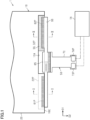
- a light control unit 1 of the first embodiment includes a light control sheet 10 and a flexible wiring board unit 50.
- the light control sheet 10 includes an edge 10E that extends in a first direction D1.
- the flexible wiring board unit 50 is connected to the edge 10E of the light control sheet 10.
- the light control sheet 10 includes a first transparent electrode sheet 20 and a second transparent electrode sheet 30.
- the first transparent electrode sheet 20 is located on a side of the second transparent electrode sheet 30 facing the front side of the paper.
- the second transparent electrode sheet 30 is located on a side of the first transparent electrode sheet 20 facing the rear side of the paper.
- the first transparent electrode sheet 20 is indicated by the thick line and the second transparent electrode sheet 30 is indicated by the thin line.
- the space where the light control sheet 10 is provided is partitioned into two spaces by the light control sheet 10.
- the space on the front side of the paper and in contact with the first transparent electrode sheet 20 is a first space.
- the space on the rear side of the paper and in contact with the second transparent electrode sheet 30 is a second space.
- the light control sheet 10 includes a first electrode terminal 22P and a second electrode terminal 32P.
- the first electrode terminal 22P is a portion of the first transparent electrode sheet 20 exposed from the second transparent electrode sheet 30.
- the first electrode terminal 22P faces the second space (in Fig. 1 , rear side of the paper).
- the second electrode terminal 32P is a portion of the second transparent electrode sheet 30 exposed from the first transparent electrode sheet 20.
- the second electrode terminal 32P faces the first space (in Fig. 1 , front side of the paper).
- the first electrode terminal 22P and the second electrode terminal 32P are arranged at a distance from each other in the first direction D1. In Fig. 1 , the first electrode terminal 22P is surrounded by the dotted line and the second electrode terminal 32P is indicated by the halftone dots.
- the edge 10E has a notch 10A.
- the notch 10A is a portion of the edge 10E recessed from the edge 10E toward the inside of the light control sheet 10.
- the notch 10A is disposed at the edge 10E between the first electrode terminal 22P and the second electrode terminal 32P.
- the flexible wiring board unit 50 includes a first flexible wiring board 60 extending in a first direction D1 and a second flexible wiring board 70 extending in a second direction D2 that intersects the first direction D1.
- the second direction D2 is perpendicular to the first direction D1.
- Each of the first flexible wiring board 60 and the second flexible wiring board 70 is a flexible printed circuit (FPC).
- the first flexible wiring board 60 includes a first bonding terminal 61P and a second bonding terminal 62P.
- the first bonding terminal 61P includes tooth terminals arranged in a comb-like manner at a predetermined pitch in the first direction D1.
- the first bonding terminal 61P is located on the second space side of the first electrode terminal 22P (in Fig. 1 , rear side of the paper).
- the first bonding terminal 61P is bonded and electrically connected to the first electrode terminal 22P while facing the first electrode terminal 22P.
- the second bonding terminal 62P includes tooth terminals arranged in a comb-like manner at a predetermined pitch in the first direction D1.
- the second bonding terminal 62P is located on the first space side of the second electrode terminal 32P (in Fig. 1 , front side of the paper).
- the second bonding terminal 62P is bonded and electrically connected to the second electrode terminal 32P while facing the second electrode terminal 32P.
- the first bonding terminal 61P and the second bonding terminal 62P are arranged in the first direction D1 in the first flexible wiring board 60.
- the first bonding terminal 61P is disposed on one side of the first flexible wiring board 60 in the first direction D1.
- the second bonding terminal 62P is disposed on the other side of the first flexible wiring board 60 in the first direction D1.
- the first bonding terminal 61P is disposed on a first side of the first flexible wiring board 60 in the first direction D1.
- the second bonding terminal 62P is disposed on a second side of the first flexible wiring board 60 opposite to the first side in the first direction D1.
- the first bonding terminal 61P and the second bonding terminal 62P are located on the second space side and the first space side relative to the light control sheet 10, respectively, with the notch 10A therebetween.
- the first flexible wiring board 60 includes a projection 65.
- the projection 65 is disposed in the first flexible wiring board 60 between the first bonding terminal 61P and the second bonding terminal 62P in the first direction D1.
- the projection 65 projects in the second direction D2 toward the light control sheet 10.
- the width of the projection 65 is smaller than the width of the notch 10A.
- the first bonding terminal 61P is appropriately positioned relative to the first electrode terminal 22P in the first direction D1.
- the second bonding terminal 62P is appropriately positioned relative to the second electrode terminal 32P in the first direction D1.
- the flexible wiring board unit 50 can be attached to an appropriate position in the first direction D1 based on the positioning of the projection 65 relative to the notch 10A.
- the flexible wiring board unit 50 has a substantially T-shaped outline formed of the first flexible wiring board 60 and the second flexible wiring board 70.
- the second flexible wiring board 70 includes a first power supply terminal 73P and a second power supply terminal 74P.
- the first power supply terminal 73P and the second power supply terminal 74P are disposed on a second side opposite to the first side in the second direction D2.
- Each of the first power supply terminal 73P and the second power supply terminal 74P is connected to an external power supply 1A.
- the external power supply 1A applies a voltage across the first transparent electrode sheet 20 and the second transparent electrode sheet 30 via the flexible wiring board unit 50. This causes the light control sheet 10 to change the light transmittance.
- the light control sheet 10 includes the first transparent electrode layer 20, the second transparent electrode sheet 30 and the light control layer 40.
- the first transparent electrode sheet 20 includes a first transparent substrate 21 and a first transparent electrode layer 22.
- the second transparent electrode sheet 30 includes a second transparent substrate 31 and a second transparent electrode layer 32.
- the light control sheet 40 is disposed between the first transparent electrode layer 22 and the second transparent electrode layer 32.
- the light control sheet 10 includes the first transparent substrate 21, the first transparent electrode layer 22, the light control layer 40, the second transparent electrode layer 32 and the second transparent substrate 31 laminated in this order.
- the first transparent substrate 21 and the second transparent substrate 31 have optical transparency to visible light and electrical insulating properties.
- the material forming the first transparent substrate 21 and the second transparent substrate 31 is an organic polymer compound or an inorganic polymer compound.
- An example of the organic polymer compound is at least one selected from the group consisting of polyesters, polyacrylates, polycarbonates and polyolefins.
- An example of the inorganic polymer compound is at least one selected from the group consisting of silicon dioxide, silicon oxynitride and silicon nitride.
- Each of the first transparent electrode layer 22 and the second transparent electrode layer 32 has optical transparency to visible light and electrical conductive properties.
- An example of the material for forming the first transparent electrode layer 22 and the second transparent electrode layer 32 is at least one selected from the group consisting of indium tin oxide, fluorine-doped tin oxide, tin oxide, zinc oxide, carbon nanotubes and poly 3,4-ethylenedioxythiophene.
- the light control layer 40 has different light transmittance before and after application of a voltage via the first transparent electrode layer 22 and the second transparent electrode layer 32.
- An example of the light control layer 40 includes a transparent organic polymer layer and a liquid crystal composition.
- the transparent organic polymer layer defines voids between the first transparent electrode layer 22 and the second transparent electrode layer 32. The voids in the transparent organic polymer layer are filled with the liquid crystal composition.
- the liquid crystal composition includes a liquid crystal compound.
- liquid crystal compound is at least one selected from the group consisting of Schiff base compounds, azo compounds, azoxy compounds, biphenyl compounds, terphenyl compounds, benzoic acid ester compounds, tolan compounds, pyrimidine compounds, cyclohexanecarboxylic acid ester compounds, phenylcyclohexane compounds and dioxane compounds.
- the type in which the transparent organic polymer layer holds the liquid crystal composition may be, for example, one selected from the group consisting of a polymer network type, polymer dispersion type and a capsule type.
- the transparent organic polymer layer has a transparent three-dimensional mesh polymer network and holds the liquid crystal composition in the interconnected mesh-like voids.
- the transparent organic polymer layer has a large number of isolated voids and holds the liquid crystal composition in the voids dispersed in the transparent organic polymer layer.
- an encapsulated liquid crystal composition is held in the transparent organic polymer layer.
- the liquid crystal composition may contain, in addition to the above-mentioned liquid crystal compound, a monomer for forming the transparent organic polymer layer, and a dichroic dye.
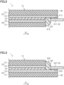
- the first electrode terminal 22P is a portion of the first transparent electrode layer 22 exposed from the second transparent electrode sheet 30 and the light control layer 40.
- the first bonding terminal 61P of the first flexible wiring board 60 is bonded and electrically connected to the first electrode terminal 22P via a first conductive adhesive 61A.
- the first conductive adhesive 61A may be, for example, at least one selected from the group consisting of an anisotropic conductive film (ACF), an anisotropic conductive paste (ACP), an isotropic conductive film (ICF) and an isotropic conductive paste (ICP).
- the first electrode terminal 22P is provided with a first sealing member 61B covering an edge face of the light control layer 40.
- the first sealing member 61B is an insulating resin. Examples of the material of the first sealing member 61B include epoxy resins and acrylic resins.
- the first sealing member 61B is in close contact with the first electrode terminal 22P while being in close contact with the edge face of the second transparent electrode sheet 30 and the edge face of the light control layer 40.
- the second electrode terminal 32P is a portion of the second transparent electrode layer 32 exposed from the first transparent electrode sheet 20 and the light control layer 40.
- the second bonding terminal 62P of the second flexible wiring board 60 is bonded and electrically connected to the second electrode terminal 32P via a second conductive adhesive 62A.
- the material of the second conductive adhesive 62A may be, for example, the same type as the first conductive adhesive 61A.
- the second electrode terminal 32P is provided with a second sealing member 62B covering an edge face of the light control layer 40.
- the second sealing member 62B is an insulating resin, and examples thereof include epoxy resins and acrylic resins.
- the second sealing member 62B is in close contact with the second electrode terminal 32P while being in close contact with the edge face of the first transparent electrode sheet 20 and the edge face of the light control layer 40.
- the first sealing member 61B and the second sealing member 62B which cover the edge face of the light control layer 40, prevents external leakage of the liquid crystal composition forming the light control layer 40 and suppresses deterioration of the liquid crystal composition due to acid, moisture, UV light, and the like.
- the first flexible wiring board 60 and the second flexible wiring board 70 are electrically connected to each other, the first direction D1 and the second direction D2 mutually intersecting.
- the first flexible wiring board 60 has a width W1 in the first direction D1 larger than a width W2 in the second direction D2.
- the second flexible wiring board 70 has a width W4 in the second direction D2 larger than a width W3 in the first direction D1.
- the width W3 is less than 50% of the width W1, and may be, for example, 30% or less.
- the width W2 is less than 50% of the width W4, and may be, for example, 30% or less.
- the first flexible wiring board 60 includes a first relay terminal 63P and a second relay terminal 64P.
- the first relay terminal 63P and the second relay terminal 64P are disposed between the first bonding terminal 61P and the second bonding terminal 62P in the first direction D1.
- the first relay terminal 63P and the second relay terminal 64P are disposed at the center of the first flexible wiring board 60 in the first direction D1.
- the first relay terminal 63P includes tooth terminals arranged in a comb-like manner at a predetermined pitch in the first direction D1.
- the first relay terminal 63P is electrically connected to the first bonding terminal 61P inside the first flexible wiring board 60.
- the first bonding terminal 61P and the first relay terminal 63P are arranged to face opposite directions with a through hole 66 therebetween.
- the first bonding terminal 61P faces the front side of the paper in Fig. 4 .
- the first relay terminal 63P faces the rear side of the paper in Fig. 4 .
- the second relay terminal 64P includes tooth terminals arranged in a comb-like manner at a predetermined pitch in the first direction D1.
- the second relay terminal 64P is electrically connected to the second bonding terminal 62P inside the first flexible wiring board 60.
- the second relay terminal 64P faces the same direction as the second bonding terminal 62P faces (in Fig. 4 , rear side of the paper). Therefore, in the first flexible wiring board 60, the direction in which the first bonding terminal 61P faces is opposite to that in which the second bonding terminal 62P, the first relay terminal 63P and the second relay terminal 64P face.
- the second flexible wiring board 70 includes a third relay terminal 71P and a fourth relay terminal 72P.
- the third relay terminal 71P and the fourth relay terminal 72P are disposed on the first side in the second direction D2 opposite to the second side on which the first power supply terminal 73P and the second power supply terminal 74P are disposed.
- the relative position of the second relay terminal 64P to the first relay terminal 63P is equal to the relative position of the fourth relay terminal 72P to the third relay terminal 71P.
- the third relay terminal 71P includes tooth terminals arranged in a comb-like manner at the same pitch as the first relay terminal 63P in the first direction D1.
- the third relay terminal 71P is electrically connected to the first power supply terminal 73P inside the first flexible wiring board 60.
- the fourth relay terminal 72P includes tooth terminals arranged in a comb-like manner at the same pitch as the second relay terminal 64P in the first direction D1.
- the fourth relay terminal 72P is electrically connected to the second power supply terminal 74P inside the first flexible wiring board 60.
- the third relay terminal 71P, the fourth relay terminal 72P, the first power supply terminal 73P and the second power supply terminal 74P face the same direction (in Fig. 4 , front side of the paper).
- the third relay terminal 71P is electrically connected to the first relay terminal 63P while facing the first relay terminal 63P.
- the fourth relay terminal 72P is electrically connected to the second relay terminal 64P while facing the second relay terminal 64P.
- an adhesive made of at least one selected from the group consisting of an anisotropic conductive film, an anisotropic conductive paste, an isotropic conductive film and an isotropic conductive paste is used.
- the first flexible wiring board 60 and the second flexible wiring board 70 are integrally connected by the connection between the first relay terminal 63P and the third relay terminal 71P and the connection between the second relay terminal 64P and the fourth relay terminal 72P.
- the first bonding terminal 61P is electrically connected to the first power supply terminal 73P via the first relay terminal 63P and the third relay terminal 71P. Therefore, the external power supply 1A is electrically connected to the first transparent electrode sheet 20 via the first power supply terminal 73P, the third relay terminal 71P, the first relay terminal 63P, the first bonding terminal 61P, the first electrode terminal 22P.
- the second bonding terminal 62P is electrically connected to the second power supply terminal 74P via the second relay terminal 64P and the fourth relay terminal 72P. Therefore, the external power supply 1Ais electrically connected to the second transparent electrode sheet 30 via the second power supply terminal 74P, the fourth relay terminal 72P, the second relay terminal 64P, the second bonding terminal 62P, the second electrode terminal 32P.
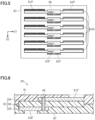
- first flexible wiring boards 60 in production of first flexible wiring boards 60, a plurality of first flexible wiring boards 60 are panelized in a first laminate sheet 80 in which materials for forming first flexible wiring boards 60 are laminated.
- first laminate sheet 80 in which materials for forming first flexible wiring boards 60 are laminated.
- first laminate sheet 80 in the first laminate sheet 80, a plurality of first flexible wiring boards 60 are panelized in the second direction D2.
- the first laminate sheet 80 has a double-sided structure which includes two outer film layers 81 and 82 and a double-sided conductive layer 83 interposed between the two outer film layers 81 and 82.
- the double-sided conductive layer 83 includes two conductive layers 84 and 85 having conductivity and an inner film layer 86 interposed between the two conductive layers 84 and 85.
- the two outer film layers 81 and 82 and the inner film layer 86 are insulating resin films, and may be made of, for example, polyimide.
- the two outer film layers 81 and 82 and the inner film layer 86 are example insulating layers.
- the two conductive layers 84 and 85 are made of, for example, copper foil.
- the conductive layer 84 is in contact with the outer film layer 81.
- the conductive layer 85 is in contact with the outer film layer 82.
- the first flexible wiring board 60 having a double-sided structure includes the outer film layer 81, the conductive layer 84, the inner film layer 86, the conductive layer 85 and the outer film layer 82 laminated in this order.
- a plurality of terminals included in each flexible wiring board face opposite directions.
- a plurality of terminals included in each flexible wiring board can be arranged to face any of two opposite directions.
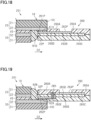
- the first bonding terminal 61P, the first relay terminal 63P and the through hole 66 are schematically illustrated in a single cross-sectional view.
- the first bonding terminal 61P is a portion where the conductive layer 84 is exposed due to the outer film layer 81 being removed.
- the first relay terminal 63P is a portion where the conductive layer 85 is removed due to the outer film layer 82 being removed.
- the first bonding terminal 61P and the first relay terminal 63P face opposite directions.
- the two conductive layers 84 and 85 disposed between the first bonding terminal 61P and the first relay terminal 63P are electrically connected to each other via the through hole 66.
- the second bonding terminal 62P and the second relay terminal 64P are portions where the conductive layer 85 is exposed due to the outer film layer 82 being removed.
- the second bonding terminal 62P and the second relay terminal 64P face the same direction as the first relay terminal 63P faces.
- the second laminate sheet 90 has a single-sided structure which includes two film layers 91 and 92 and a conductive layer 93 interposed between the two film layers 91 and 92.
- the two film layers 91 and 92 are insulating resin films, and may be made of, for example, polyimide.
- the two film layers 91 and 92 are example insulating layers.
- the conductive layer 93 is made of, for example, copper foil.
- the second flexible wiring board 70 having a single-sided structure includes the film layer 91, the conductive layer 93 and the film layer 92 laminated in this order.
- the second flexible wiring board 70 having a single-sided structure includes fewer layers in the lamination direction than the first flexible wiring board 60 having a double-sided structure does.
- a plurality of terminals in each flexible wiring board face in one direction.
- a plurality of terminals included in each flexible wiring board are arranged to face one same direction.
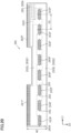
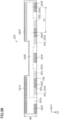
- the third relay terminal 71P, the fourth relay terminal 72P, the first power supply terminal 73P and the second power supply terminal 74P are schematically illustrated in a single cross-sectional view.
- the third relay terminal 71P, the fourth relay terminal 72P, the first power supply terminal 73P and the second power supply terminal 74P are portions where the conductive layer 93 is exposed due to the film layer 91 being removed.
- the third relay terminal 71P, the fourth relay terminal 72P, the first power supply terminal 73P and the second power supply terminal 74P face the same direction.
- the first flexible wiring board 60 and the second flexible wiring board 70 which extend in different directions, are separately produced and then integrally connected to each other. Accordingly, the first flexible wiring boards 60 can be efficiently panelized in the first laminate sheet 80, increasing the yield. Similarly, the second flexible wiring boards 70 can be efficiently panelized in the second laminate sheet 90, increasing the yield. Therefore, the yield can be improved compared to the case where the first flexible wiring board 60 and the second flexible wiring boards 70 are produced as a single flexible wiring board.
- Producing the first flexible wiring board 60 and the second flexible wiring board 70 separately makes it possible to provide the first flexible wiring board 60 with a double-sided structure while providing the second flexible wiring board 70 with a single-sided structure. If the first flexible wiring board 60 and the second flexible wiring board 70 are produced as a single flexible wiring board, the entire flexible wiring board is formed of the first laminate sheet 80 having a double-sided structure. Compared to the first laminate sheet 80 having a double-sided structure, the second laminate sheet 90 having a single-sided structure has reduced thickness due to the fewer constituent layers, and thus has high flexibility and bending resistance. In addition, the production cost is reduced due to the fewer constituent layers.
- the second flexible wiring board 70 can simplify the layer configuration and increase the flexibility. Further, compared to the case where the entire flexible wiring board unit 50 has a double-sided structure, the production cost can be reduced.
- the first relay terminal 63P and the second relay terminal 64P are arranged to face the same direction in the first flexible wiring board 60.
- the third relay terminal 71P and the fourth relay terminal 72P are arranged to face the same direction in the second flexible wiring board 70. Therefore, the connection between the first relay terminal 63P and the third relay terminal 71P and the connection between the second relay terminal 64P and the fourth relay terminal 72P can be simultaneously performed. Accordingly, the connection between the first flexible wiring board 60 and the second flexible wiring board 70 can be efficiently performed.
- the first embodiment can be modified and implemented as follows.
- the modifications described below can be combined with each other as long as no technical contradiction occurs.
- a light control unit 101 of the second embodiment includes the same light control sheet 10 as in the first embodiment and a flexible wiring board unit 150.
- the flexible wiring board unit 150 is connected to the edge 10E of the light control sheet 10.
- the flexible wiring board unit 150 includes a first flexible wiring board 160 extending in a first direction D1 and a second flexible wiring board 170 extending in a second direction D2 that intersects the first direction D1.
- the first flexible wiring board 160 and the second flexible wiring board 170 are electrically connected to each other, the first direction D1 and the second direction D2 mutually intersecting.
- the first flexible wiring board 160 is responsible for electrical connection to the light control sheet 10, which is a power supply target, in the flexible wiring board unit 150.
- the second flexible wiring board 170 is responsible for electrical connection to the external power supply 1A in the flexible wiring board unit 150.
- the first flexible wiring board 160 and the second flexible wiring board 170 is a flexible printed circuit (FPC).
- the first flexible wiring board 160 includes a first bonding terminal 161 and a second bonding terminal 162.
- the first bonding terminal 161 and the second bonding terminal 162 are arranged in the first direction D1 in the first flexible wiring board 160.
- the first bonding terminal 161 is disposed on one side of the first flexible wiring board 160 in the first direction D1.
- the second bonding terminal 162 is disposed on the other side of the first flexible wiring board 160 in the first direction D1.
- the first bonding terminal 161 is disposed on a first side of the first flexible wiring board 160 in the first direction D1.
- the second bonding terminal 162 is disposed on a second side of the first flexible wiring board 160 opposite to the first side in the first direction D1.
- the first bonding terminal 161 is located on the second space side of the first electrode terminal 22P (in Fig. 9 , rear side of the paper), and faces the first space side (in Fig. 9 , front side of the paper).
- the first bonding terminal 161 includes a plurality of first bonding tooth terminals 161P arranged in a comb-like manner at a predetermined pitch in the first direction D1.
- the first bonding tooth terminals 161P are bonded and electrically connected to the first electrode terminal 22P while facing the first electrode terminal 22P.
- the second bonding terminal 162 is located on the first space side of the second electrode terminal 32P (in Fig. 9 , front side of the paper), and faces the second space side (in Fig. 9 , rear side of the paper).
- the second bonding terminal 162 includes a plurality of second bonding tooth terminals 162P arranged in a comb-like manner at a predetermined pitch in the first direction D1.
- the second bonding tooth terminals 162P are bonded and electrically connected to the second electrode terminal 32P while facing the second electrode terminal 32P.
- the first flexible wiring board 160 includes a first relay terminal 163 and a second relay terminal 164.
- the first relay terminal 163 and the second relay terminal 164 are arranged in the first flexible wiring board 160 at a predetermined distance from each other in the second direction D2.
- the first relay terminal 163 and the second relay terminal 164 face the first space side (in Fig. 9 , front side of the paper).
- the first bonding terminal 161 and the second bonding terminal 162 are disposed on one side of the first flexible wiring board 160 in the second direction D2.
- the second relay terminal 164 is positioned on the other side of the first flexible wiring board 160 in the second direction D2, which is opposite to the side on which the first bonding terminal 161 and the second bonding terminal 162 are positioned.
- the first bonding terminal 161 and the second bonding terminal 162 are disposed on a first side of the first flexible wiring board 160 in the second direction D2.
- the second relay terminal 164 is disposed on the side of the first flexible wiring board 160 opposite to the side on which the first bonding terminal 161 and the second bonding terminal 162 are disposed in the second direction D2, that is, on a second side opposite to the first side.
- the first relay terminal 163 is disposed between the first and second bonding terminals 161 and 162 and the second relay terminal 164 in the second direction D2.
- the first relay terminal 163 includes a plurality of first tooth terminals 163P arranged in a comb-like manner at a predetermined pitch in the first direction D1.
- the plurality of first tooth terminals 163P are arranged in the first direction D1 from the position of the first bonding terminal 161 to the position of the second bonding terminal 162.
- the second relay terminal 164 includes a plurality of second tooth terminals 164P arranged in a comb-like manner at a predetermined pitch in the first direction D1.
- the plurality of second tooth terminals 164P are arranged in the first direction D1 from the position of the first bonding terminal 161 to the position of the second bonding terminal 162.
- a first side of the second flexible wiring board 170 in the second direction D2 is physically and electrically connected to the first flexible wiring board 160.
- the second flexible wiring board 170 extends in the second direction D2 from the connection with the first flexible wiring board 160 toward the outside of the light control sheet 10.
- the flexible wiring board unit 150 has a substantially T-shaped outline formed of the first flexible wiring board 160 and the second flexible wiring board 170.
- the second flexible wiring board 170 includes a third relay terminal 171 and a fourth relay terminal 172.
- the third relay terminal 171 and the fourth relay terminal 172 are disposed on the first side of the second flexible wiring board 170 in the second direction D2.
- the third relay terminal 171 and the fourth relay terminal 172 are arranged in the first direction D1 while the fourth relay terminal 172 is spaced at a predetermined distance from the third relay terminal 171 in the second direction D2.
- the third relay terminal 171 and the fourth relay terminal 172 face the second space side (in Fig. 9 , rear side of the paper).
- the third relay terminal 171 includes a plurality of third tooth terminals 171P arranged in a comb-like manner at a predetermined pitch in the first direction D1.
- the fourth relay terminal 172 includes a plurality of fourth tooth terminals 172P arranged in a comb-like manner at a predetermined pitch in the first direction D1.
- the first tooth terminals 163P, the second tooth terminals 164P, the third tooth terminals 171P and the fourth tooth terminals 172P are arranged at the same pitch.
- the number of the first tooth terminals 163P is the same as the number of the second tooth terminals 164P.
- the number of the third tooth terminals 171P is the same as the number of the fourth tooth terminals 172P.
- the number of the first tooth terminals 163P is greater than the number of the third tooth terminals 171P.
- the number of the second tooth terminals 164P is greater than the number of the fourth tooth terminals 172P.
- Each of the third tooth terminals 171P is physically and electrically connected to corresponding one of the plurality of first tooth terminals 163P.
- each of the fourth tooth terminals 172P is physically and electrically connected to corresponding one of the plurality of second tooth terminals 164P. Accordingly, the first flexible wiring board 160 and the second flexible wiring board 170 are physically and electrically connected.
- the second flexible wiring board 170 includes a first power supply terminal 173P and a second power supply terminal 174P.
- the first power supply terminal 173P and the second power supply terminal 174P are disposed on the second side in the second direction D2 opposite to the first side on which the third relay terminal 171 and the fourth relay terminal 172 are disposed.
- Each of the first power supply terminal 173P and the second power supply terminal 174P is connected to the external power supply 1A.
- the external power supply 1A applies a voltage across the first transparent electrode sheet 20 and the second transparent electrode sheet 30 via the flexible wiring board unit 150. This causes the light control sheet 10 to change the light transmittance.
- the light control sheet 10 is an example power supply target to which the external power supply 1A supplies power via the flexible wiring board unit 150.
- the first flexible wiring board 160 includes a first outer insulating layer 160A, a second outer insulating layer 160B, an inner insulating layer 160C, a first conductive layer 160D and a second conductive layer 160E (see Fig. 11 ).
- the inner insulating layer 160C is disposed between the first outer insulating layer 160A and the second outer insulating layer 160B.
- the first outer insulating layer 160A is located on a side of the inner insulating layer 160C facing the first space which is partitioned by the light control sheet 10.
- the second outer insulating layer 160B is located on a side of the inner insulating layer 160C facing the second space partitioned by the light control sheet 10.
- the first outer insulating layer 160A, the second outer insulating layer 160B and the inner insulating layer 160C are insulating resin films, and may be made of, for example, polyimide.
- the first conductive layer 160D is disposed between the first outer insulating layer 160A and the inner insulating layer 160C.
- the second conductive layer 160E is disposed between the second outer insulating layer 160B and the inner insulating layer 160C.
- the first conductive layer 160D and the second conductive layer 160E are conductive metal films, and may be made of, for example, copper foil. In the cross-section shown in Fig. 10 , the second conductive layer 160E is not disposed. Further, the first conductive layer 160D shown in Fig. 10 is electrically isolated from the first conductive layer 160D shown in Fig. 11 .
- the first flexible wiring board 160 having a double-sided structure includes the first outer insulating layer 160A, the first conductive layer 160D, the inner insulating layer 160C, the second conductive layer 160E and the second outer insulating layer 160B laminated in this order.
- the first bonding terminal 161 and the first relay terminal 163 are portions of the first flexible wiring board 160 where the first conductive layer 160D is exposed from the first outer insulating layer 160A.
- the first bonding terminal 161 is electrically connected to the first relay terminal 163 via the first conductive layer 160D inside the first flexible wiring board 160.
- the first bonding terminal 161 is electrically connected to the first electrode terminal 22P via the first conductive adhesive 61A.
- the first electrode terminal 22P is provided with a first sealing member 61B covering an edge face of the light control layer 40.
- the second bonding terminal 162 of the first flexible wiring board 160 is bonded and electrically connected to the second electrode terminal 32P via the second conductive adhesive 62A.
- the second electrode terminal 32P is provided with a second sealing member 62B covering an edge face of the light control layer 40.
- the first relay terminal 163 and the second relay terminal 164 have the same length in the first direction D1.
- the second relay terminal 164 is displaced by a distance L1 from the first relay terminal 163 in the first direction D1 toward the second bonding terminal 162.
- the first flexible wiring board 160 includes a plurality of through holes 165 between the second bonding terminal 162-side end and the first relay terminal 163 in the first direction D1.
- the second relay terminal 164 is spaced at a predetermined distance L2 from the first relay terminal 163 in the second direction D2.
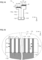
- the first tooth terminals 163P will be described.
- the first conductive layer 160D is indicated by thin halftone dots. Since the second tooth terminals 164P have the same configuration as that of the first tooth terminals 163P, the detailed description thereof will be omitted.
- a plurality of first tooth terminals 163P are arranged at a predetermined pitch P1 in the first direction D1.
- Each of the first tooth terminals 163P has a first projection 166.
- the first projection 166 is an example of a reference portion for arranging the third tooth terminals 171P in appropriate positions relative to the first tooth terminals 163P in each of the first direction D1 and the second direction D2.
- the first projection 166 projects from the side edge of the first tooth terminal 163P from the first bonding terminal 161-side toward the second bonding terminal 162-side in the first direction D1.
- the length from the center of a portion of the first tooth terminal 163P extending in the second direction D2 to the tip of the first projection 166 is a distance L3.
- the first projection 166 is disposed at substantially the center of the first tooth terminals 163P in the second direction D2.
- the second flexible wiring board 170 includes a third outer insulating layer 170A, a fourth outer insulating layer 170B and a conductive layer 170C.
- the conductive layer 170C is disposed between the third outer insulating layer 170A and the fourth outer insulating layer 170B
- the third outer insulating layer 170A is located on the first space side of the conductive layer 170C (in Fig. 14 , rear side of the paper).
- the fourth outer insulating layer 170B is located on the second space side of the conductive layer 170C (in Fig. 14 , front side of the paper).
- the third outer insulating layer 170A and the fourth outer insulating layer 170B are insulating resin films, and may be made of, for example, polyimide.
- the conductive layer 170C is a conductive metal film, and may be made of, for example, copper foil.
- the second flexible wiring board 170 having a single-sided structure includes the third outer insulating layer 170A, the conductive layer 170C and the fourth outer insulating layer 170B laminated in this order.
- the second flexible wiring board 170 having a single-sided structure includes fewer layers in the lamination direction than the first flexible wiring board 160 having a double-sided structure does.
- the third relay terminal 171, the fourth relay terminal 172, the first power supply terminal 173P and the second power supply terminal 174P of the second flexible wiring board 170 are portions where the conductive layer 170C is exposed from the fourth outer insulating layer 170B.
- the conductive layer 170C electrically connects the third relay terminal 171 with the first power supply terminal 173P and electrically connects the fourth relay terminal 172 with the second power supply terminal 174P inside the second flexible wiring board 170. Further, in the conductive layer 170C, a portion connecting the third relay terminal 171 with the first power supply terminal 173P is electrically insulated from a portion connecting the fourth relay terminal 172 with the second power supply terminal 174P.
- the length of the third relay terminal 171 is the same as the length of the fourth relay terminal 172.
- a distance L4 from the end of the third relay terminal 171 farther from the fourth relay terminal 172 to the end of the fourth relay terminal 172 closer to the third relay terminal 171 is equal to the distance L1.
- the fourth relay terminal 172 is spaced at a predetermined distance L5 from the third relay terminal 171. The distance L5 is equal to the distance L2.
- each of the fourth tooth terminals 172P is electrically connected to corresponding one of the plurality of second tooth terminals 164P.
- the third relay terminal 171 is positioned relative to the fourth relay terminal 172 such that when each of the third tooth terminals 171P is connected to the first tooth terminals 163P, each of the fourth tooth terminals 172P is connected to the second tooth terminals 164P.
- the second bonding terminal 162 is disposed to face the direction opposite to that in which the first bonding terminal 161, the first relay terminal 163 and the second relay terminal 164 face due to the three insulating layers 160A to 160C and two conductive layers 160D and 160E.
- the third relay terminal 171, the fourth relay terminal 172, the first power supply terminal 173P and the second power supply terminal 174P are disposed to face the same direction due to the two insulating layers 170A and 170B and one conductive layer 170C.
- the layer configuration of the second flexible wiring board 170 can be simplified. As a result, the bending resistance and flexibility of the second flexible wiring board 170 can be improved due to the fewer constituent layers.
- a plurality of third tooth terminals 171P are arranged at a predetermined pitch P1 in the first direction D1.
- the third tooth terminal 171P positioned on each end in the first direction D1 has two second projections 175.
- the second projection 175 is an example of a registration portion for arranging the third tooth terminals 171P in appropriate positions relative to the first tooth terminals 163P in each of the first direction D1 and the second direction D2.
- the second projections 175 project from the side edge of the third tooth terminals 171P from the third relay terminal 171-side toward the fourth relay terminal 172-side in the first direction D1.
- the length from the center of a portion of the third tooth terminal 171P extending in the second direction D2 to the tip of the second projection 175 is a distance L6.
- the distance L6 is greater than the distance L3.
- the two second projections 175 are arranged in the second direction D2 at an interval greater than the width of the first projection 166.
- Each of the third tooth terminals 171P faces and is electrically connected to corresponding one of the plurality of first tooth terminals 163P.
- each of the fourth tooth terminals 172P faces and is electrically connected to corresponding one of the plurality of second tooth terminals 164P.
- an adhesive made of at least one selected from the group consisting of an anisotropic conductive film, an anisotropic conductive paste, an isotropic conductive film and an isotropic conductive paste is used.
- the first flexible wiring board 160 and the second flexible wiring board 170 are integrally connected by the connection between the first tooth terminals 163P and the third tooth terminals 171P and the connection between the second tooth terminals 164P and the fourth tooth terminals 172P.
- the first tooth terminals 163P and the second tooth terminals 164P face the same direction and the third tooth terminals 171P and the fourth tooth terminals 172P face the same direction. Therefore, the connection between the first tooth terminals 163P and the third tooth terminals 171P and the connection between the second tooth terminals 164P and the fourth tooth terminals 172P can be simultaneously performed.
- the arrangement of the third tooth terminals 171P relative to the first tooth terminals 163P and the arrangement of the fourth tooth terminals 172P relative to the second tooth terminals 164P can be varied for each pitch P1. That is, in the flexible wiring board unit 150, the arrangement of the second flexible wiring board 170 relative to the first flexible wiring board 160 in the first direction D1 can be varied for each pitch P1.
- the first bonding terminal 161 is electrically connected to the external power supply 1A via the first relay terminal 163, the third relay terminal 171 and the first power supply terminal 173P.
- the second bonding terminal 162 is electrically connected to the external power supply 1A via the second relay terminal 164, the fourth relay terminal 172 and the second power supply terminal 174P.
- the first tooth terminal 163P that is not connected to the third tooth terminal 171P may be sealed by, for example, applying and curing an insulating resin paste.
- the second tooth terminal 164P that is not connected to the fourth tooth terminal 172P may be sealed by, for example, applying and curing an insulating resin paste.
- the connection between the first tooth terminals 163P and the third tooth terminals 171P will be described.
- the first conductive layer 160D of the first flexible wiring board 160 is indicated by thin halftone dots and the conductive layer 170C is indicated by thick halftone dots. Since the second tooth terminals 164P and the fourth tooth terminals 172P have the same configuration as that of the first tooth terminals 163P and the third tooth terminals 171P, the detailed description thereof will be omitted.
- Each of the third tooth terminals 171P overlaps and is electrically connected to corresponding one of the plurality of first tooth terminals 163P.
- the first projection 166 of the first tooth terminal 163P is positioned between two second projections 175 in the second direction D2.
- the tips of the two second projections 175 are located between adjacent first tooth terminals 163P and between the first projection 166 and the side edge of the first tooth terminal 163P closest to the first projection 166.
- the first projection 166 is located inside a recess formed by the side edge of the third tooth terminal 171P and two second projections 175.
- the first tooth terminals 163P are arranged in appropriate positions relative to the third tooth terminals 171P in each of the first direction D1 and the second direction D2. That is, based on the relative positioning of the first projection 166 and the two second projections 175, the third tooth terminals 171P can be arranged in appropriate positions relative to the first tooth terminals 163P in each of the first direction D1 and the second direction D2.
- the positioning using the first projection 166 and the second projection 175 is performed in the third tooth terminal 171P located on each end in the first direction D1 among the plurality of third tooth terminals 171P.
- This makes it possible to arrange each of the third tooth terminals 171P of the third relay terminal 171 in an appropriate position relative to the first tooth terminal 163P to which it is connected.
- the first projection 166 is provided in each of the first tooth terminals 163P. Therefore, regardless of which of the first tooth terminals 163P the third tooth terminal 171P having two second projections 175 is connected to, the two second projections 175 can be arranged in appropriate positions relative to the first projection 166, and thus the third tooth terminals 171P can be arranged in appropriate positions relative to the first tooth terminals 163P.
- the second embodiment can be modified and implemented as follows.
- the modifications described below can be combined with each other as long as no technical contradiction occurs.
- a light control unit 201 of the third embodiment includes the same light control sheet 10 as in the first embodiment and a flexible wiring board unit 250.
- the flexible wiring board unit 250 is connected to the edge 10E of the light control sheet 10.
- the flexible wiring board unit 250 includes a first flexible wiring board 260 extending in a first direction D1 and a second flexible wiring board 270 extending in a second direction D2 that intersects the first direction D1.
- the first flexible wiring board 260 and the second flexible wiring board 270 are electrically connected to each other, the first direction D1 and the second direction D2 mutually intersecting.
- the first flexible wiring board 260 is responsible for electrical connection to the light control sheet 10, which is a power supply target, in the flexible wiring board unit 250.
- the second flexible wiring board 270 is responsible for electrical connection to the external power supply 1A in the flexible wiring board unit 250.
- the first flexible wiring board 260 and the second flexible wiring board 270 is a flexible printed circuit (FPC).
- the first flexible wiring board 260 includes a first bonding terminal 261P and a second bonding terminal 262P.
- the first bonding terminal 261P and the second bonding terminal 262P are arranged in the first direction D1 in the first flexible wiring board 260.
- the first bonding terminal 261P is disposed on one side of the first flexible wiring board 260 in the first direction D1.
- the second bonding terminal 262P is disposed on the other side of the first flexible wiring board 260 in the first direction D1.
- the first bonding terminal 261P is disposed on a first side of the first flexible wiring board 260 in the first direction D1.
- the second bonding terminal 262P is disposed on a second side of the first flexible wiring board 260 opposite to the first side in the first direction D1.
- the first bonding terminal 261P is located on the second space side of the first electrode terminal 22P (in Fig. 17 , rear side of the paper), and faces the first space side (in Fig. 17 , front side of the paper).
- the first bonding terminal 261P includes a plurality of tooth terminals arranged in a comb-like manner at a predetermined pitch in the first direction D1.
- the first bonding terminal 261P is bonded and electrically connected to the first electrode terminal 22P while facing the first electrode terminal 22P.
- the second bonding terminal 262P is located on the first space side of the second electrode terminal 32P (in Fig. 17 , front side of the paper), and faces the second space side (in Fig. 17 , rear side of the paper).
- the second bonding terminal 262P includes a plurality of tooth terminals arranged in a comb-like manner at a predetermined pitch in the first direction D1.
- the second bonding terminal 262P is bonded and electrically connected to the second electrode terminal 32P while facing the second electrode terminal 32P.
- the first flexible wiring board 260 includes a plurality of first relay terminals 263P and a plurality of second relay terminals 264P.
- the plurality of first relay terminals 263P and the plurality of second relay terminals 264P are alternately arranged in a row in the first direction D1.
- the first relay terminals 263P and the second relay terminals 264P face the first space side (in Fig. 17 , front side of the paper).
- Each of the first relay terminals 263P and each of the second relay terminals 264P includes a plurality of tooth terminals arranged in a comb-like manner at a predetermined pitch in the first direction D1.
- Each of the first relay terminals 263P and each of the second relay terminals 264P has the same number of tooth terminals arranged at the same pitch. In this example, the number of the first relay terminals 263P is the same as that of the second relay terminals 264P, but the number of the first relay terminals 263P may be greater or smaller than that of the second relay terminals 264P.
- Each of the first relay terminals 263P is electrically connected to the first bonding terminal 261P inside the first flexible wiring board 260.
- Each of the second relay terminals 264P is electrically connected to the second bonding terminal 262P via a plurality of through holes 265 inside the first flexible wiring board 60.
- a first side of the second flexible wiring board 270 in the second direction D2 is physically and electrically connected to the first flexible wiring board 260.
- the second flexible wiring board 270 extends in the second direction D2 from the connection with the first flexible wiring board 260 toward the outside of the light control sheet 10.
- the flexible wiring board unit 250 has a substantially T-shaped outline formed of the first flexible wiring board 260 and the second flexible wiring board 270.
- the second flexible wiring board 270 includes a third relay terminal 271P and a fourth relay terminal 272P.
- the third relay terminal 271P and the fourth relay terminal 272P are disposed on the first side of the second flexible wiring board 270 in the second direction D2.
- the third relay terminal 271P and the fourth relay terminal 272P are arranged in the first direction D1.
- the third relay terminal 271P and the fourth relay terminal 272P face the second space side (in Fig. 17 , rear side of the paper).
- the third relay terminal 271P and the fourth relay terminal 272P include a plurality of tooth terminals arranged in a comb-like manner at a predetermined pitch in the first direction D1.
- the number of tooth terminals and the pitch of tooth terminals included in the third relay terminal 271P and the fourth relay terminal 272P are the same. Further, the number of tooth terminals and the pitch of tooth terminals included in the third relay terminal 271P and the fourth relay terminal 272P are the same as those in each of the first relay terminals 263P and each of the second relay terminals 264P.
- the third relay terminal 271P is connected to one of adjacent first relay terminal 263P and second relay terminal 264P among the plurality of first relay terminals 263P and the plurality of second relay terminals 264P arranged in a row.
- the fourth relay terminal 272P is connected to the other of adjacent first relay terminal 263P and second relay terminal 264P among the plurality of first relay terminals 263P and the plurality of second relay terminals 264P arranged in a row. Accordingly, the first flexible wiring board 260 and the second flexible wiring board 270 are physically and electrically connected.
- the second flexible wiring board 270 includes a first power supply terminal 273P and a second power supply terminal 274P.
- the first power supply terminal 273P and the second power supply terminal 274P are disposed on the second side in the second direction D2 opposite to the first side on which the third relay terminal 271P and the fourth relay terminal 272P are disposed.
- Each of the first power supply terminal 273P and the second power supply terminal 274P is connected to the external power supply 1A.
- the external power supply 1A applies a voltage across the first transparent electrode sheet 20 and the second transparent electrode sheet 30 via the flexible wiring board unit 250. This causes the light control sheet 10 to change the light transmittance.
- the light control sheet 10 is an example power supply target to which the external power supply 1A supplies power via the flexible wiring board unit 250.
- the second outer insulating layer 260B is located on a side of the inner insulating layer 260C facing the second space partitioned by the light control sheet 10.
- the first outer insulating layer 260A, the second outer insulating layer 260B and the inner insulating layer 260C are insulating resin films, and may be made of, for example, polyimide.
- the first conductive layer 260D is disposed between the first outer insulating layer 260A and the inner insulating layer 260C.
- the second conductive layer 260E is disposed between the second outer insulating layer 260B and the inner insulating layer 260C.
- the first conductive layer 260D and the second conductive layer 260E are conductive metal films, and may be made of, for example, copper foil. In the cross-section shown in Fig. 18 , the second conductive layer 260E is not disposed. Further, the first conductive layer 260D shown in Fig. 18 is electrically isolated from the first conductive layer 260D shown in Fig. 19 .
- the first flexible wiring board 260 having a double-sided structure includes the first outer insulating layer 260A, the first conductive layer 260D, the inner insulating layer 260C, the second conductive layer 260E and the second outer insulating layer 260B laminated in this order.
- the first bonding terminal 261P and the first relay terminal 263P are portions of the first flexible wiring board 260 where the first conductive layer 260D is exposed from the first outer insulating layer 260A.
- the first bonding terminal 261P is electrically connected to the first relay terminal 263P via the first conductive layer 260D inside the first flexible wiring board 260.
- the first bonding terminal 261P is electrically conductively bonded to the first electrode terminal 22P via the first conductive adhesive 61A.
- the first electrode terminal 22P is provided with a first sealing member 61B covering an edge face of the light control layer 40.
- the second bonding terminal 262P is a portion of the first flexible wiring board 260 where the second conductive layer 260E is exposed from the second outer insulating layer 260B.
- the second relay terminal 264P is a portion of the first flexible wiring board 260 where the first conductive layer 260D is exposed from the first outer insulating layer 260A.
- the second conductive layer 260E constituting the second bonding terminal 262P and the first conductive layer 260D constituting the second relay terminal 264P are electrically connected via a through hole 265.
- the second bonding terminal 262P of the first flexible wiring board 260 is electrically conductively bonded to the second electrode terminal 32P via the second conductive adhesive 62A.
- the second electrode terminal 32P is provided with a second sealing member 62B covering an edge face of the light control layer 40.
- the first conductive layer 260D includes a first portion 260D1 and a second portion 260D2.
- the first portion 260D1 constitutes the first bonding terminal 261P and the first relay terminals 263P of the first conductive layer 260D while connecting the first bonding terminal 261P to each of the first relay terminals 263P.
- the first bonding terminal 261P is disposed on one side in the second direction D2 and the respective first relay terminals 263P are disposed on the other side in the second direction D2.
- the first conductive layer 260D extends in the second direction D2 from the first bonding terminal 261P to each of the first relay terminals 263P.
- the second portion 260D2 constitutes the second bonding terminal 262P of the first conductive layer 260D.
- One side of the second portion 260D2 overlaps the second conductive layer 260E via the inner insulating layer 260C, and is connected to the second conductive layer 260E via a plurality of through holes 265.
- the plurality of through holes 265 are positioned on the second bonding terminal 262P-side end of the first flexible wiring board 260 in the first direction D1.
- the plurality of through holes 265 are positioned between the second bonding terminal 262P and each of the second relay terminals 264P in the second direction D2.
- the number of through holes 265 may be determined according to the magnitude of current flowing through the second portion 260D2 and the second conductive layer 260E, and may be, for example, one or two or more.
- the portion where the second portion 260D2 overlaps the second conductive layer 260E via the inner insulating layer 260C and where the plurality of through holes 265 are provided is an example of an interlayer connection section 265A where the first conductive layer 260D is electrically connected to the second conductive layer 260E.
- the interlayer connection section 265A is positioned between the second bonding terminal 262P and each of the second relay terminals 264P in the second direction D2.
- the interlayer connection section 265A is disposed at a position displaced toward the second bonding terminal 262P-side from the center of the first flexible wiring board 260 in the first direction D1. Further, in the first direction D1, the width of the interlayer connection section 265A is smaller than the width of the second bonding terminal 262P.
- the interlayer connection section 265A is a portion including the through holes 265, it has relatively poor flexibility and low bending resistance compared to the other portions in the first flexible wiring board 260.
- a decrease in the flexibility and bending resistance of the first flexible wiring board 260 as a whole can be suppressed.
- concentrating the plurality of through holes 265 in a single location within a small area in plan view in a direction perpendicular to the first flexible wiring board 260 a decrease in the flexibility and bending resistance of the first flexible wiring board 260 as a whole can be suppressed.
- the width of the interlayer connection section 265A smaller than the width of the second bonding terminal 262P and by positioning the interlayer connection section 265A displaced toward the second bonding terminal 262P-side, a decrease in bending resistance against bending in a direction parallel to the first direction D1 can be suppressed.
- the second portion 260D2 extends in the second direction D2 from the interlayer connection section 265A toward the side of the first flexible wiring board 260 opposite to that on which the second bonding terminal 262P is disposed.
- the second portion 260D2 extends between the side edge of the first flexible wiring board 260 extending in the second direction D2 on the second bonding terminal 262P-side and the second relay terminal 264P closest to that side edge.
- the second portion 260D2 extends in the first direction D1 between the side edge of the first flexible wiring board 260 extending in the first direction D1 on a side opposite to that on which the second bonding terminal 262P is located and the respective second relay terminals 264P, and also extends toward the second bonding terminal 262P-side to form the respective second relay terminals 264P.
- the plurality of first relay terminals 263P and the plurality of second relay terminals 64P are alternately arranged at a predetermined pitch P2 in the first direction D1.
- the first flexible wiring board 260 has a width W5 in the second direction D2.
- the tips of the tooth terminals having a comb-like shape extend away from the first bonding terminal 261P.
- the tips of the tooth terminals having a comb-like shape extend toward the second bonding terminal 262P.
- Each of the first relay terminals 263P and each of the second relay terminals 264P has a reference portion 266.
- each reference portion 266 is provided on both ends of the respective first relay terminals 263P and the respective second relay terminals 264P in the first direction D1.
- the reference portion 266 may be, for example, a crusiform projection.
- the reference portion 266 serves as a reference for appropriately arranging the terminals when the third relay terminal 271P or the fourth relay terminal 272P is connected to the first relay terminal 263P or the second relay terminal 264P.
- the second flexible wiring board 270 includes a third outer insulating layer 270A, a fourth outer insulating layer 270B and a conductive layer 270C.
- the conductive layer 270C is disposed between the third outer insulating layer 270A and the fourth outer insulating layer 270B.
- the third outer insulating layer 270A is located on the first space side of the conductive layer 270C (in Fig. 21 , rear side of the paper).
- the fourth outer insulating layer 270B is located on the second space side of the conductive layer 270C (in Fig. 21 , front side of the paper).
- the third outer insulating layer 270A and the fourth outer insulating layer 270B are insulating resin films, and may be made of, for example, polyimide.
- the conductive layer 270C is a conductive metal film, and may be made of, for example, copper foil.
- the second flexible wiring board 270 having a single-sided structure includes the third outer insulating layer 270A, the conductive layer 270C and the fourth outer insulating layer 270B laminated in this order.
- the second flexible wiring board 270 having a single-sided structure includes fewer layers in the lamination direction than the first flexible wiring board 260 having a double-sided structure does.
- the third relay terminal 271P, the fourth relay terminal 272P, the first power supply terminal 273P and the second power supply terminal 274P of the second flexible wiring board 270 are portions of the second flexible wiring board 270 where the conductive layer 270C is exposed from the fourth outer insulating layer 270B.
- the conductive layer 270C electrically connects the third relay terminal 271P with the first power supply terminal 273P and electrically connects the fourth relay terminal 272P with the second power supply terminal 274P inside the second flexible wiring board 270. Further, in the conductive layer 270C, a portion connecting the third relay terminal 271P with the first power supply terminal 273P is electrically insulated from a portion connecting the fourth relay terminal 272P with the second power supply terminal 274P.
- a pitch P3 from the center of the third relay terminal 271P to the center of the fourth relay terminal 272P is the same as the pitch P2 at which the first relay terminals 263P and the second relay terminals 264P are arranged.
- Each of the third relay terminal 271P and the fourth relay terminal 272P has a registration portion 275.
- the registration portion 275 is provided on both ends of the third relay terminal 271P and the fourth relay terminal 272P in the first direction D1.
- the registration portion 275 may be, for example, a crusiform recess.
- the reference portion 266 and the registration portion 275 can be combined to appropriately arrange the terminals.
- the third relay terminal 271P is connected to the first relay terminals 263P
- the projection of the reference portion 266 is positioned inside the recess of the registration portion 275 so that the third relay terminal 271P is appropriately arranged relative to the first relay terminals 263P.
- the third relay terminal 271P and the fourth relay terminal 272P can be appropriately arranged relative to the first relay terminal 263P or the second relay terminal 264P based on the arrangement of the registration portion 275 relative to the reference portion 266.
- the second bonding terminal 262P is disposed to face the direction opposite to that in which the first bonding terminal 261P, the first relay terminal 263P and the second relay terminal 264P face due to the three insulating layers 260A to 260C and two conductive layers 260D and 260E.
- the third relay terminal 271P, the fourth relay terminal 272P, the first power supply terminal 273P and the second power supply terminal 274P are disposed to face the same direction due to the two insulating layers 270A and 270B and one conductive layer 270C.
- the layer configuration of the second flexible wiring board 270 can be simplified. As a result, the bending resistance and flexibility of the second flexible wiring board 270 can be improved due to the fewer constituent layers.
- the third relay terminal 271P is connected to corresponding one of the plurality of first relay terminals 263P or corresponding one of the plurality of second relay terminals 264P.
- the fourth relay terminal 272P is connected to the other of the plurality of first relay terminals 263P and the plurality of second relay terminals 264P in the other of the first relay terminal 263P and second relay terminal 264P, respectively, which is the relay terminal adjacent to the relay terminal to which the third relay terminal 271P is connected.
- the fourth relay terminal 272P is connected to the second relay terminal 264P adjacent to the first relay terminal 263P to which the third relay terminal 271P is connected.
- the fourth relay terminal 272P is connected to the first relay terminal 263P adjacent to the second relay terminal 264P to which the third relay terminal 271P is connected.
- the fourth relay terminal 272P is electrically connected to the other of the first relay terminal 263P and the second relay terminal 264P.
- the fourth relay terminal 272P is disposed relative to the third relay terminal 271P in a plane including the first direction D1 and the second direction D2 so that the above connection can be performed.
- the arrangement of the third relay terminal 271P and the fourth relay terminal 272P relative to the terminal row formed of the plurality of first relay terminals 263P and the plurality of second relay terminals 264P can be varied. Accordingly, in the flexible wiring board unit 250, the arrangement of the second flexible wiring board 270 relative to the first flexible wiring board 260 in the first direction D1 can be varied for each pitch P2.
- an adhesive made of at least one selected from the group consisting of an anisotropic conductive film, an anisotropic conductive paste, an isotropic conductive film and an isotropic conductive paste is used.
- the first flexible wiring board 260 and the second flexible wiring board 270 are integrally connected by the connection between one of the plurality of first relay terminals 263P and one of the plurality of second relay terminals 264P to the third relay terminal 271P and the fourth relay terminal 272P.
- the first relay terminals 263P and the second relay terminals 264P face the same direction, and the third relay terminal 271P and the fourth relay terminal 272P face the same direction. Therefore, the connection between the third relay terminal 271P and one of the first relay terminal 263P and the second relay terminal 264P and the connection between the fourth relay terminal 272P and the other of the first relay terminal 263P and the second relay terminal 264P can be simultaneously performed.
- first relay terminal 263P and the second relay terminal 264P that are not connected to either the third relay terminal 271P or the fourth relay terminal 272P may be sealed by, for example, applying and curing an insulating resin paste.
- the circuit configuration of the flexible wiring board unit 250 will be described.
- the third relay terminal 271P is connected to the first relay terminal 263P
- the fourth relay terminal 272P is connected to the second relay terminal 264P.
- the first bonding terminal 261P is electrically connected to the external power supply 1A via the first relay terminal 263P, the third relay terminal 271P and the first power supply terminal 273P.
- the second bonding terminal 262P is electrically connected to the external power supply 1A via the second relay terminal 264P, the fourth relay terminal 272P and the second power supply terminal 274P.
- the third relay terminal 271P is connected to the second relay terminal 264P
- the fourth relay terminal 272P is connected to the first relay terminal 263P.
- the first bonding terminal 261P is electrically connected to the external power supply 1A via the first relay terminal 263P, the fourth relay terminal 272P and the second power supply terminal 274P.
- the second bonding terminal 262P is electrically connected to the external power supply 1Avia the second relay terminal 264P, the third relay terminal 271P and the first power supply terminal 273P.
- Alight control unit of the fourth embodiment has the same configuration as that of the light control unit 201 of the third embodiment except that a first flexible wiring board 280 is provided instead of the first flexible wiring board 260.
- the first flexible wiring board 280 includes, as with the first flexible wiring board 260, the first bonding terminal 261P, the second bonding terminal 262P, a plurality of first relay terminals 263P and a plurality of second relay terminals 264P.
- the first bonding terminal 261P, the first relay terminals 263P and the second relay terminals 264P are formed of the first conductive layer 260D.
- the second bonding terminal 262P is formed of the second conductive layer 260E.
- the second conductive layer 260E is connected to the first portion 260D1 that connects the first bonding terminal 261P and the first relay terminals 263P via a plurality of through holes 265. That is, between the first bonding terminal 261P and the first relay terminals 263P, the interlayer connection section 265A is provided in which the first conductive layer 260D and the second conductive layer 260E are electrically connected via a plurality of through holes 265. In Fig. 22 , the interlayer connection section 265A is indicated by the dots.
- the interlayer connection section 265A positioned between the first bonding terminal 261P and the first relay terminals 263P extends in the first direction D1 from one end to the other end of a terminal row formed of the plurality of first relay terminals 263P.
- the interlayer connection section 265A positioned between the first bonding terminal 261P and the first relay terminals 263P includes one or more through holes 265 at positions, for example, at least adjacent to each of the first relay terminals 263P.
- the width in the second direction D2 of a portion formed as the interlayer connection section 265A is smaller than the width of a portion formed only of the first conductive layer 260D.
- the portions other than the second bonding terminal 262P and the second relay terminals 264P are electrically connected via a plurality of through holes 265. That is, between the second bonding terminal 62P and the second relay terminals 264P, the interlayer connection section 265A is provided in which the first conductive layer 260D and the second conductive layer 260E are electrically connected via a plurality of through holes 265.
- the interlayer connection section 265A that connects the second bonding terminal 262P and the second relay terminals 264P includes one or more through holes 265 at positions, for example, at least adjacent to each of the first relay terminals 263P.
- the width in the second direction D2 of a portion located on a side of the second relay terminals 264P opposite to that on which the second bonding terminal 262P is located is smaller than the width of a portion formed only of the first conductive layer 260D.
- the interlayer connection section 265A connects the first bonding terminal 261P and the first relay terminals 263P and connects the second bonding terminal 262P and the second relay terminals 264P.
- a width W6 of the first flexible wiring board 280 in the second direction D2 can be made smaller than the width W5 of the first flexible wiring board 260 while suppressing an increase in the amount of heat generation due to current flow.
- the width W6 of the first flexible wiring board 280 can be made smaller than the width W5 of the first flexible wiring board 60 while suppressing heat generation due to current flow.
- the interlayer connection section 265A between the second bonding terminal 262P and the second relay terminals 264P may be disposed at least on a side of the second relay terminals 264P opposite to that on which the second bonding terminal 262P is located (in Fig. 22 , right side of the paper relative to the second bonding terminal 262P). Further, the interlayer connection section 265A may extend in the first direction D1 from one end to the other end of the terminal row formed of the plurality of second relay terminals 264P.
- the width W6 of the first flexible wiring board 280 can be made smaller than the width W5 of the first flexible wiring board 260 while suppressing an increase in the amount of heat generation due to current flow.
- the width W6 of the first flexible wiring board 280 can be made smaller than the width W5 of the first flexible wiring board 260 while suppressing heat generation due to current flow. Therefore, while the flexible wiring board unit 250 is connected to the light control sheet 10, the length of the first flexible wiring board 280 protruding from the light control sheet 10 can be reduced. Further, the flexible wiring board unit 250 including the first flexible wiring board 280 can also achieve the advantageous effects similar to the above (1-1), (3-1) to (3-3) and (3-5).
- a light control unit of the fifth embodiment has the same configuration as that of the light control unit 201 of the third embodiment except that a first flexible wiring board 281 is provided instead of the first flexible wiring board 260.
- the first flexible wiring board 281 includes, as with the first flexible wiring board 260, the first bonding terminal 261P, the second bonding terminal 262P, a plurality of first relay terminals 263P and a plurality of second relay terminals 264P.
- the first relay terminals 263P and the second relay terminals 264P are disposed on the second side of the first flexible wiring board 281 in the second direction D2 opposite to the first side on which the first bonding terminal 261P and the second bonding terminal 262P are disposed. Further, in the first relay terminals 263P and the second relay terminals 264P, the tips of the tooth terminals having a comb-like shape extend away from the first bonding terminal 261P and the second bonding terminal 262P.
- the first bonding terminal 261P, the first relay terminals 263P and the second relay terminals 264P are formed of the first conductive layer 260D.
- the second bonding terminal 262P is formed of the second conductive layer 260E.
- the outline of a portion of the first conductive layer 260D overlapping the first outer insulating layer 260A is indicated by the dotted line.
- the first bonding terminal 261P is disposed on one side in the second direction D2 and the respective first relay terminals 263P are disposed on the other side in the second direction D2.
- the first conductive layer 260D extends in the second direction D2 from the first bonding terminal 261P to each of the first relay terminals 263P.
- the second portions 260D2 constituting the second relay terminals 264P are discontinuously disposed. In other words, the second portions 260D2 are provided in the same number as the number of the second relay terminals 264P. Each of the second portions 260D2 extends in the second direction D2 from the second relay terminal 264P toward the second bonding terminal 262P.
- the second bonding terminal 262P is disposed on one side in the second direction D2 and the other side in the second direction D2 overlaps each of the second portions 260D2 constituting the second relay terminals 264P.
- the outline of the second conductive layer 260E is indicated by the dotted line.
- the portions where the second conductive layer 260E overlaps each of the second portions 260D2 constitute the interlayer connection sections 265A in which the second conductive layer 260E is electrically connected to each of the second portions 260D2 via a plurality of through holes 265. That is, in the first flexible wiring board 281, the interlayer connection section 265A is provided for each of the second relay terminals 264P. In the first flexible wiring board 281, the second relay terminal 264P and the interlayer connection section 265A are arranged side by side in the second direction D2 such that the interlayer connection sections 265A are located on the second bonding terminal 262P-side of the second relay terminals 264P.
- the second conductive layer 260E connecting the second bonding terminal 262P and each of the second relay terminals 264P and the second portions 260D2 are positioned between the second bonding terminal 262P and each of the second relay terminals 264P in the second direction D2.
- the first relay terminals 263P and the second relay terminals 264P can be disposed on one side (edge) of the first flexible wiring board 281 in the second direction D2.
- the wiring path connecting the second bonding terminal 262P and each of the second relay terminals 264P can be made shorter.
- a width W7 of the first flexible wiring board 281 in the second direction D2 can be made smaller than the width W5 of the first flexible wiring board 260.
- the width W7 of the first flexible wiring board 281 in the second direction D2 can be made smaller than the width W5 of the first flexible wiring board 260.
- the flexible wiring board unit 250 including the first flexible wiring board 281 can also achieve the advantageous effects similar to the above (1-1), (3-1) to (3-3) and (3-5).
- a light control unit of the sixth embodiment has the same configuration as that of the light control unit 201 of the third embodiment except that a first flexible wiring board 282 is provided instead of the first flexible wiring board 260.
- the first flexible wiring board 282 includes, as with the first flexible wiring board 260, the first bonding terminal 261P, the second bonding terminal 262P, a plurality of first relay terminals 263P and a plurality of second relay terminals 264P.
- the first relay terminals 263P and the second relay terminals 264P are disposed on the second side of the first flexible wiring board 282 in the second direction D2 opposite to the first side on which the first bonding terminal 261P and the second bonding terminal 262P are disposed. Further, in the first relay terminals 263P and the second relay terminals 264P, the tips of the tooth terminals having a comb-like shape extend away from the first bonding terminal 261P and the second bonding terminal 262P.
- the pitch P2 at which the first relay terminals 263P and the second relay terminals 264P are alternately arranged is greater than the pitch P2 in the first flexible wiring board 260 of the third embodiment. Therefore, in the second flexible wiring board 270 of the sixth embodiment, the pitch P3 from the center of the third relay terminal 271P to the center of the fourth relay terminal 272P is greater than that in the third embodiment.
- the first bonding terminal 261P, the first relay terminals 263P and the second relay terminals 264P are formed of the first conductive layer 260D.
- the second bonding terminal 262P is formed of the second conductive layer 260E.
- the outline of a portion of the first conductive layer 260D overlapping the first outer insulating layer 260A is indicated by the dotted line.
- the first bonding terminal 261P is disposed on one side in the second direction D2 and the respective first relay terminals 263P are disposed on the other side in the second direction D2.
- the first conductive layer 260D extends in the second direction D2 from the first bonding terminal 261P to each of the first relay terminals 263P.
- the second portions 260D2 constituting the second relay terminals 264P are discontinuously disposed. In other words, the second portions 260D2 are provided in the same number as the number of the second relay terminals 264P. Each of the second portions 260D2 extends in the first direction D1 from the second relay terminal 264P to the first relay terminals 263P located on both sides of the second relay terminal 264P.
- the second bonding terminal 262P is disposed on one side in the second direction D2 and the other side in the second direction D2 overlaps each of the second portions 260D2 constituting the second relay terminals 264P.
- the outline of the second conductive layer 260E is indicated by the dotted line.
- the portions where the second conductive layer 260E overlaps each of the second portions 260D2 constitute the interlayer connection sections 265A in which the second conductive layer 260E is electrically connected to each of the second portions 260D2 via a plurality of through holes 265. That is, in the first flexible wiring board 282, the interlayer connection section 265A is provided for each of the second relay terminals 264P. Each of the interlayer connection sections 265A is disposed on both sides of each of the second relay terminals 264P in the first direction D1. In one example, the interlayer connection sections 265A are disposed on both sides of the second relay terminal 264P between two first relay terminals 263P. The interlayer connection sections 265A may be disposed adjacent to at least one side of each of the second relay terminals 264P in the first direction D1.
- the first relay terminals 263P and the second relay terminals 264P can be disposed on one side of the first flexible wiring board 282 in the second direction D2.
- the wiring path connecting the second bonding terminal 262P and each of the second relay terminals 264P can be made shorter.
- a width W8 of the first flexible wiring board 282 in the second direction D2 can be made smaller than the width W5 of the first flexible wiring board 260.
- the second relay terminals 264P and the interlayer connection sections 265A are arranged side by side in the first direction D1. Therefore, compared to the first flexible wiring board 281 of the fifth embodiment, the width W8 can be made smaller than the width W7 due to the absence of the interlayer connection section 265A between the second bonding terminal 262P and the second relay terminal 264P in the second direction D2.
- the pitch P2 can be made smaller due to the absence of the interlayer connection section 265A between the first relay terminal 263P and the second relay terminal 264P. Therefore, in the first direction D1, the arrangement of the second flexible wiring board 270 relative to the first flexible wiring board 281 can be varied at shorter intervals.
- a light control unit of the seventh embodiment has the same configuration as that of the light control unit 201 of the third embodiment except that a first flexible wiring board 283 and a second flexible wiring board 290 are provided instead of the first flexible wiring board 260 and the second flexible wiring board 270.
- the first flexible wiring board 283 includes the first bonding terminal 261P, the second bonding terminal 262P, a plurality of first relay terminals 263P and a plurality of second relay terminals 264P.
- the first bonding terminal 261P and the plurality of first relay terminals 263P face the first space partitioned by the light control sheet 10 (in Fig. 27 , front side of the paper).
- the second bonding terminal 262P and the plurality of second relay terminals 264P face the second space partitioned by the light control sheet 10 (in Fig. 27 , rear side of the paper). Therefore, the first relay terminals 263P and the second relay terminals 264P face opposite directions.
- the first bonding terminal 261P and the first relay terminals 263P are formed of the first conductive layer 260D.
- the outline of a portion of the first conductive layer 260D overlapping the first outer insulating layer 260A is indicated by the dotted line.
- the second bonding terminal 262P and the second relay terminals 264P are formed of the second conductive layer 260E.
- the second bonding terminal 262P and the second relay terminals 264P are portions where the second conductive layer 260E is exposed from the second outer insulating layer 260B to the second space.
- Each of the first relay terminals 263P and each of the second relay terminals 264P are disposed on the second side of the first flexible wiring board 283 in the second direction D2 opposite to the first side on which the first bonding terminal 261P and the second bonding terminal 262P are disposed. Further, in the first relay terminals 263P and the second relay terminals 264P, the tips of the tooth terminals having a comb-like shape extend away from the first bonding terminal 261P and the second bonding terminal 262P.
- the first bonding terminal 261P is disposed on one side in the second direction D2 and the respective first relay terminals 263P are disposed on the other side in the second direction D2.
- the first conductive layer 260D extends in the second direction D2 from the first bonding terminal 261P to each of the first relay terminals 263P.
- the second bonding terminal 262P is disposed on one side in the second direction D2 and the respective second relay terminals 264P are disposed on the other side in the second direction D2.
- the outline of the second conductive layer 260E is indicated by the dotted line.
- the second conductive layer 260E extends in the second direction D2 from the second bonding terminal 262P to each of the second relay terminals 264P.
- the first relay terminals 263P and the second relay terminals 264P can be disposed on one side of the first flexible wiring board 283 in the second direction D2.
- the wiring path connecting the second bonding terminal 262P and each of the second relay terminals 264P can be made shorter.
- a width W9 of the first flexible wiring board 283 in the second direction D2 can be made smaller than the width W5 of the first flexible wiring board 260.
- first flexible wiring board 283 In the case of the first flexible wiring board 283, a structure such as the through hole 265 for electrically connecting the first conductive layer 260D and the second conductive layer 260E is not necessary. Therefore, the flexibility and bending resistance of the first flexible wiring board 283 can be improved.
- the second flexible wiring board 290 includes a third outer insulating layer 290A, a fourth outer insulating layer 290B, an inner insulating layer 290C, a third conductive layer 290D and a fourth conductive layer 290E.
- the inner insulating layer 290C is disposed between the third outer insulating layer 290A and the fourth outer insulating layer 290B.
- the third outer insulating layer 290A is located on a side of the inner insulating layer 290C facing the first space partitioned by the light control sheet 10 (in Fig. 29 , rear side of the paper).
- the fourth outer insulating layer 290B is located on a side of the inner insulating layer 290C facing the second space partitioned by the light control sheet 10 (in Fig. 29 , front side of the paper).
- the third outer insulating layer 290A, the fourth outer insulating layer 290B and the inner insulating layer 290C are insulating resin films, and may be made of, for example, polyimide.
- the third conductive layer 290D is disposed between the third outer insulating layer 290A and the inner insulating layer 290C.
- the fourth conductive layer 290E is disposed between the fourth outer insulating layer 290B and the inner insulating layer 290C.
- the third conductive layer 290D and the fourth conductive layer 290E are conductive metal films, and may be made of, for example, copper foil.
- the second flexible wiring board 290 having a double-sided structure includes the third outer insulating layer 290A, the third conductive layer 290D, the inner insulating layer 290C, the fourth conductive layer 290E and the fourth outer insulating layer 290B laminated in this order.
- the third relay terminal 271P, the first power supply terminal 273P and the second power supply terminal 274P are portions where the fourth conductive layer 290E is exposed from the fourth outer insulating layer 290B to the second space.
- the fourth relay terminal 272P is a portion where the third conductive layer 290D is exposed from the third outer insulating layer 290A to the first space. Therefore, the third relay terminal 271P and the fourth relay terminal 272P face opposite directions.
- the third relay terminal 271P is electrically connected to the first power supply terminal 273P via the fourth conductive layer 290E inside the second flexible wiring board 290. Further, in the fourth conductive layer 290E, portions constituting the third relay terminal 271P and the first power supply terminal 273P are electrically insulated from a portion constituting the second power supply terminal 274P.
- the third conductive layer 290D constituting the fourth relay terminal 272P is electrically connected to a portion of the fourth conductive layer 290E constituting the second power supply terminal 274P via a plurality of through holes 291. Therefore, the fourth relay terminal 272P is electrically connected to the second power supply terminal 274P via the third conductive layer 290D, the fourth conductive layer 290E and the through hole 291 inside the second flexible wiring board 290.
- the number of through holes 291 may be one or may be two or more.
- connection of the third relay terminal 271P to one of the first relay terminal 263P and the second relay terminal 264P and the connection of the fourth relay terminal 272P to the other of the first relay terminal 263P and the second relay terminal 264P are performed separately.
- the third to seventh embodiments can be modified and implemented as follows.
- the modifications described below can be combined with each other as long as no technical contradiction occurs.
- the first to seventh embodiments can be modified and implemented as follows.
- the modifications described below can be combined with each other as long as no technical contradiction occurs.
Landscapes
- Engineering & Computer Science (AREA)
- Microelectronics & Electronic Packaging (AREA)
- Physics & Mathematics (AREA)
- Nonlinear Science (AREA)
- Manufacturing & Machinery (AREA)
- Mathematical Physics (AREA)
- Chemical & Material Sciences (AREA)
- Crystallography & Structural Chemistry (AREA)
- General Physics & Mathematics (AREA)
- Optics & Photonics (AREA)
- Combinations Of Printed Boards (AREA)
- Structure Of Printed Boards (AREA)
Abstract
Description
- The present disclosure relates to a flexible wiring board unit including a plurality of electrically connectable flexible wiring boards, and a light control unit including the flexible wiring board unit.
- A light control sheet includes two transparent electrode sheets and a light control layer disposed between the two transparent electrode sheets. The respective transparent electrode sheets include an electrode terminal. The electrode terminal is a portion of each transparent electrode sheet exposed from the light control layer and the other transparent electrode sheet. The electrode terminals included in the respective transparent electrode sheets are disposed at an edge of the light control sheet. Each of the electrode terminals is bonded to respective bonding terminals included in a flexible wiring board (see e.g.,
PTLs 1 and 2). As a voltage is applied across the two transparent electrode sheets via the flexible wiring board, the light control sheet changes light transmittance of the light control layer from that before the voltage is applied. - For example, as shown in
Fig. 30 , alight control sheet 300 includes a firsttransparent electrode sheet 310, a second transparent electrode sheet 320, and a light control layer disposed between the firsttransparent electrode sheet 310 and the second transparent electrode sheet 320. InFig. 30 , the firsttransparent electrode sheet 310 is located on a side of the second transparent electrode sheet 320 facing the front side of the paper. Further, inFig. 30 , for convenience of description of the shape of the respective sheets, the firsttransparent electrode sheet 310 is indicated by the bold line and the second transparent electrode sheet 320 is indicated by the thin line. - The first
transparent electrode sheet 310 includes thefirst terminal 310P. Thefirst terminal 310P, indicated by the dotted line inFig. 30 , is a portion of the firsttransparent electrode sheet 310 exposed from the second transparent electrode sheet 320 and the light control layer. Thefirst terminal 310P faces toward the rear side of the paper inFig. 30 . The second transparent electrode sheet 320 includes the second terminal 320P. The second terminal 320P, indicated by the halftone dots inFig. 30 , is a portion of the second transparent electrode sheet 320 exposed from the firsttransparent electrode sheet 310 and the light control layer. The second terminal 320P faces toward the front side of the paper inFig. 30 . - The
light control sheet 300 has anedge 300E that extends in a first direction D1. Thefirst terminal 310P and the second terminal 320P are arranged side by side at theedge 300E. Part of theedge 300E is notched to form a notch 300E1 between thefirst terminal 310P and the second terminal 320P. - The
light control sheet 300 is connected to anexternal power source 340 via aflexible wiring board 330. Theflexible wiring board 330 is a flexible printed circuit (FPC). Theflexible wiring board 330 includes afirst portion 331 and asecond portion 332. Thefirst portion 331 extends in the first direction D1. Thesecond portion 332 extends, from the center of thefirst portion 331 in the first direction D1, toward the outside of thelight control sheet 300 in a second direction D2 perpendicular to the first direction D1. Theflexible wiring board 330 has a substantially T-shaped outline formed of thefirst portion 331 and thesecond portion 332. - The
first portion 331 includes a first bonding terminal 331P1 and a second bonding terminal 331P2. The first bonding terminal 331P1 is disposed on a first side of thefirst portion 331 in the first direction D1. The second bonding terminal 331P2 is disposed on a second side of thefirst portion 331 opposite to the first side in the first direction D1. The first bonding terminal 331P1 faces toward the front side of the paper inFig. 30 . The first bonding terminal 331P1 is electrically connected to thefirst terminal 310P. The second bonding terminal 331P2 faces toward the rear side of the paper inFig. 30 . The second bonding terminal 331P2 is electrically connected to the second terminal 320P. - The
second portion 332 includes a first power supply terminal 332P1 and a second power supply terminal 332P2. The first power supply terminal 332P1 and the second power supply terminal 332P2 are disposed at the edge of thesecond portion 332 in the second direction D2. The first power supply terminal 332P1 and the second power supply terminal 332P2 face toward the front side of the paper inFig. 30 . The first power supply terminal 332P1 is electrically connected to the first bonding terminal 331P1 inside theflexible wiring board 330. The second power supply terminal 332P2 is electrically connected to the second bonding terminal 331P2 inside theflexible wiring board 330. The first power supply terminal 332P1 and the second power supply terminal 332P2 are electrically connected to theexternal power supply 340. Theexternal power supply 340 applies a voltage across the firsttransparent electrode sheet 310 and the second transparent electrode sheet 320 via theflexible wiring board 330. This causes the light control layer to change the light transmittance. -
- PTL 1:
JP 2007-57925 A - PTL 2:
JP 2020-38265 A - As shown in
Fig. 31 , in production offlexible wiring boards 330, a plurality offlexible wiring boards 330 are panelized in alaminate sheet 400 composed of two resin material layers and a conductor sandwiched therebetween. In the example shown inFig. 31 , theflexible wiring boards 330 adjacent to each other in the second direction D2 are arranged while being alternately flipped 180 degrees. - In production of
flexible wiring boards 330, since the ratio of the area used for theflexible wiring boards 330 to the total area of thelaminate sheet 400 is small, it is required to improve the yield. In particular, as thelight control sheet 300 increases in size, the larger the width W331 of thefirst portion 331 in the first direction D1, the smaller the ratio of the area used for theflexible wiring boards 330 to the area of thelaminate sheet 400. Similarly, the larger the width W332 of thesecond portion 332 in the second direction D2, the smaller the ratio of the area used for theflexible wiring boards 330 to the total area of thelaminate sheet 400. - In one aspect, a flexible wiring board unit is provided. A flexible wiring board unit includes: a first flexible wiring board extending in a first direction; and a second flexible wiring board extending in a second direction, wherein the second flexible wiring board is configured to be electrically connected to the first flexible wiring board on a first side of the second flexible wiring board in the second direction, the first direction and the second direction mutually intersecting, the first flexible wiring board includes a first bonding terminal and a second bonding terminal arranged in the first direction, the first bonding terminal and the second bonding terminal are configured to be connected to a power supply target, the second flexible wiring board includes a first power supply terminal and a second power supply terminal disposed on a second side which is opposite to the first side in the second direction, and the first power supply terminal and the second power supply terminal are configured to be connected to an external power supply.
- In another aspect, a light control unit is provided. A light control unit includes: a light control sheet having an edge extending in a first direction; and a flexible wiring board unit bonded to the edge, wherein the light control sheet includes: a first transparent electrode sheet; a second transparent electrode sheet; and a light control layer disposed between the first transparent electrode sheet and the second transparent electrode sheet, a portion of the first transparent electrode sheet exposed from the light control layer and the second transparent electrode sheet is a first electrode terminal, a portion of the second transparent electrode sheet exposed from the light control layer and the first transparent electrode sheet is a second electrode terminal, the first electrode terminal and the second electrode terminal are arranged in the first direction at the edge, the flexible wiring board unit includes: a first flexible wiring board extending in the first direction; and a second flexible wiring board extending in the second direction, the second flexible wiring board is configured to be electrically connected to the first flexible wiring board on a first side of the second flexible wiring board in the second direction, the first direction and the second direction mutually intersecting, the first flexible wiring board includes a first bonding terminal and a second bonding terminal arranged in the first direction, the first bonding terminal is configured to be electrically connected to the first electrode terminal, the second bonding terminal is configured to be electrically connected to the second electrode terminal, the second flexible wiring board includes a first power supply terminal and a second power supply terminal disposed on a second side which is opposite to the first side in the second direction, and the first power supply terminal and the second power supply terminal are configured to be connected to an external power supply.
-
-
Fig. 1 is a plan view of a light control unit of a first embodiment. -
Fig. 2 is a cross-sectional view taken along the line II-II inFig. 1 . -
Fig. 3 is a cross-sectional view taken along the line III-III inFig. 1 . -
Fig. 4 is a plan view of a first flexible wiring board and a second flexible wiring board included in a flexible wiring board unit of the first embodiment. -
Fig. 5 is a plan view illustrating an example panelization of the first flexible wiring boards of the first embodiment. -
Fig. 6 is a cross-sectional view of a first laminate sheet for producing a first flexible wiring board of the first embodiment. -
Fig. 7 is a plan view illustrating an example panelization of the second flexible wiring boards of the first embodiment. -
Fig. 8 is a cross-sectional view of a second laminate sheet for producing a second flexible wiring board of the first embodiment. -
Fig. 9 is a plan view of a light control unit of a second embodiment. -
Fig. 10 is a cross-sectional view taken along the line X-X inFig. 9 . -
Fig. 11 is a cross-sectional view taken along the line XI-XI inFig. 9 . -
Fig. 12 is a plan view of a first flexible wiring board included in a flexible wiring board unit of the second embodiment. -
Fig. 13 is an enlarged view of a main part of a first relay terminal of a first flexible wiring board of the second embodiment. -
Fig. 14 is a plan view of a second flexible wiring board included in a flexible wiring board unit of the second embodiment. -
Fig. 15 is an enlarged view of a main part of a third relay terminal of a second flexible wiring board of the second embodiment. -
Fig. 16 is a schematic view illustrating a relative positional relationship between a first relay terminal and a third relay terminal in a state in which the first relay terminal and the third relay terminal of the second embodiment are bonded to each other. -
Fig. 17 is a plan view of a light control unit of a third embodiment. -
Fig. 18 is a cross-sectional view taken along the line XVIII-XVIII inFig. 17 . -
Fig. 19 is a cross-sectional view taken along the line XIX-XIX inFig. 17 . -
Fig. 20 is a plan view of a first flexible wiring board of the third embodiment. -
Fig. 21 is a plan view of a second flexible wiring board of the third embodiment. -
Fig. 22 is a plan view of a first flexible wiring board of a fourth embodiment. -
Fig. 23 is a plan view of a first flexible wiring board of a fifth embodiment. -
Fig. 24 is a plan view of a first flexible wiring board of a fifth embodiment. -
Fig. 25 is a plan view of a first flexible wiring board of a sixth embodiment. -
Fig. 26 is a plan view of a first flexible wiring board of a sixth embodiment. -
Fig. 27 is a plan view of a first flexible wiring board of a seventh embodiment. -
Fig. 28 is a plan view of a first flexible wiring board of a seventh embodiment. -
Fig. 29 is a plan view of a second flexible wiring board of a seventh embodiment. -
Fig. 30 is a plan view illustrating a conventional example of a light control sheet and a flexible wiring board. -
Fig. 31 is a plan view illustrating a panelization example of the flexible wiring board shown inFig. 30 . - With reference to
Figs. 1 to 8 , a light control unit of a first embodiment will be described below. - As shown in
Fig. 1 , alight control unit 1 of the first embodiment includes alight control sheet 10 and a flexiblewiring board unit 50. Thelight control sheet 10 includes anedge 10E that extends in a first direction D1. The flexiblewiring board unit 50 is connected to theedge 10E of thelight control sheet 10. - The
light control sheet 10 includes a firsttransparent electrode sheet 20 and a secondtransparent electrode sheet 30. InFig. 1 , the firsttransparent electrode sheet 20 is located on a side of the secondtransparent electrode sheet 30 facing the front side of the paper. InFig. 1 , the secondtransparent electrode sheet 30 is located on a side of the firsttransparent electrode sheet 20 facing the rear side of the paper. Further, inFig. 1 , for the convenience of description of the relative positions of the firsttransparent electrode sheet 20 and the secondtransparent electrode sheet 30, the firsttransparent electrode sheet 20 is indicated by the thick line and the secondtransparent electrode sheet 30 is indicated by the thin line. - The space where the
light control sheet 10 is provided is partitioned into two spaces by thelight control sheet 10. InFig. 1 , of the two spaces partitioned by thelight control sheet 10, the space on the front side of the paper and in contact with the firsttransparent electrode sheet 20 is a first space. InFig. 1 , of the two spaces partitioned by thelight control sheet 10, the space on the rear side of the paper and in contact with the secondtransparent electrode sheet 30 is a second space. - The
light control sheet 10 includes afirst electrode terminal 22P and asecond electrode terminal 32P. Thefirst electrode terminal 22P is a portion of the firsttransparent electrode sheet 20 exposed from the secondtransparent electrode sheet 30. Thefirst electrode terminal 22P faces the second space (inFig. 1 , rear side of the paper). Thesecond electrode terminal 32P is a portion of the secondtransparent electrode sheet 30 exposed from the firsttransparent electrode sheet 20. Thesecond electrode terminal 32P faces the first space (inFig. 1 , front side of the paper). Thefirst electrode terminal 22P and thesecond electrode terminal 32P are arranged at a distance from each other in the first direction D1. InFig. 1 , thefirst electrode terminal 22P is surrounded by the dotted line and thesecond electrode terminal 32P is indicated by the halftone dots. - The
edge 10E has anotch 10A. Thenotch 10A is a portion of theedge 10E recessed from theedge 10E toward the inside of thelight control sheet 10. The notch 10Ais disposed at theedge 10E between thefirst electrode terminal 22P and thesecond electrode terminal 32P. - The flexible
wiring board unit 50 includes a firstflexible wiring board 60 extending in a first direction D1 and a secondflexible wiring board 70 extending in a second direction D2 that intersects the first direction D1. In one example, the second direction D2 is perpendicular to the first direction D1. Each of the firstflexible wiring board 60 and the secondflexible wiring board 70 is a flexible printed circuit (FPC). - The first
flexible wiring board 60 includes afirst bonding terminal 61P and asecond bonding terminal 62P. In one example, thefirst bonding terminal 61P includes tooth terminals arranged in a comb-like manner at a predetermined pitch in the first direction D1. Thefirst bonding terminal 61P is located on the second space side of thefirst electrode terminal 22P (inFig. 1 , rear side of the paper). Thefirst bonding terminal 61P is bonded and electrically connected to thefirst electrode terminal 22P while facing thefirst electrode terminal 22P. - In one example, the
second bonding terminal 62P includes tooth terminals arranged in a comb-like manner at a predetermined pitch in the first direction D1. Thesecond bonding terminal 62P is located on the first space side of thesecond electrode terminal 32P (inFig. 1 , front side of the paper). Thesecond bonding terminal 62P is bonded and electrically connected to thesecond electrode terminal 32P while facing thesecond electrode terminal 32P. - The
first bonding terminal 61P and thesecond bonding terminal 62P are arranged in the first direction D1 in the firstflexible wiring board 60. Thefirst bonding terminal 61P is disposed on one side of the firstflexible wiring board 60 in the first direction D1. Thesecond bonding terminal 62P is disposed on the other side of the firstflexible wiring board 60 in the first direction D1. In other words, thefirst bonding terminal 61P is disposed on a first side of the firstflexible wiring board 60 in the first direction D1. Thesecond bonding terminal 62P is disposed on a second side of the firstflexible wiring board 60 opposite to the first side in the first direction D1. In the firstflexible wiring board 60, thefirst bonding terminal 61P and thesecond bonding terminal 62P are located on the second space side and the first space side relative to thelight control sheet 10, respectively, with thenotch 10A therebetween. - The first
flexible wiring board 60 includes aprojection 65. Theprojection 65 is disposed in the firstflexible wiring board 60 between thefirst bonding terminal 61P and thesecond bonding terminal 62P in the first direction D1. Theprojection 65 projects in the second direction D2 toward thelight control sheet 10. In the first direction D1, the width of theprojection 65 is smaller than the width of thenotch 10A. When the flexiblewiring board unit 50 is attached to thelight control sheet 10, theprojection 65 is positioned inside thenotch 10A. - For example, when the
projection 65 is disposed inside thenotch 10A, it is preferred that thefirst bonding terminal 61P is appropriately positioned relative to thefirst electrode terminal 22P in the first direction D1. A the same time, it is preferred that thesecond bonding terminal 62P is appropriately positioned relative to thesecond electrode terminal 32P in the first direction D1. In this case, the flexiblewiring board unit 50 can be attached to an appropriate position in the first direction D1 based on the positioning of theprojection 65 relative to thenotch 10A. - In the second
flexible wiring board 70, a first side of the secondflexible wiring board 70 in the second direction D2 is physically and electrically connected to the firstflexible wiring board 60 at the center of the firstflexible wiring board 60 in the first direction D1. The secondflexible wiring board 70 extends in the second direction D2 from the connection with the firstflexible wiring board 60 toward the outside of thelight control sheet 10. The flexiblewiring board unit 50 has a substantially T-shaped outline formed of the firstflexible wiring board 60 and the secondflexible wiring board 70. - The second
flexible wiring board 70 includes a firstpower supply terminal 73P and a secondpower supply terminal 74P. The firstpower supply terminal 73P and the secondpower supply terminal 74P are disposed on a second side opposite to the first side in the second direction D2. Each of the firstpower supply terminal 73P and the secondpower supply terminal 74P is connected to an external power supply 1A. The external power supply 1A applies a voltage across the firsttransparent electrode sheet 20 and the secondtransparent electrode sheet 30 via the flexiblewiring board unit 50. This causes thelight control sheet 10 to change the light transmittance. - As shown in
Fig.2 , thelight control sheet 10 includes the firsttransparent electrode layer 20, the secondtransparent electrode sheet 30 and thelight control layer 40. The firsttransparent electrode sheet 20 includes a firsttransparent substrate 21 and a firsttransparent electrode layer 22. The secondtransparent electrode sheet 30 includes a secondtransparent substrate 31 and a secondtransparent electrode layer 32. Thelight control sheet 40 is disposed between the firsttransparent electrode layer 22 and the secondtransparent electrode layer 32. In thelight control sheet 10 includes the firsttransparent substrate 21, the firsttransparent electrode layer 22, thelight control layer 40, the secondtransparent electrode layer 32 and the secondtransparent substrate 31 laminated in this order. - The first
transparent substrate 21 and the secondtransparent substrate 31 have optical transparency to visible light and electrical insulating properties. The material forming the firsttransparent substrate 21 and the secondtransparent substrate 31 is an organic polymer compound or an inorganic polymer compound. An example of the organic polymer compound is at least one selected from the group consisting of polyesters, polyacrylates, polycarbonates and polyolefins. An example of the inorganic polymer compound is at least one selected from the group consisting of silicon dioxide, silicon oxynitride and silicon nitride. - Each of the first
transparent electrode layer 22 and the secondtransparent electrode layer 32 has optical transparency to visible light and electrical conductive properties. An example of the material for forming the firsttransparent electrode layer 22 and the secondtransparent electrode layer 32 is at least one selected from the group consisting of indium tin oxide, fluorine-doped tin oxide, tin oxide, zinc oxide, carbon nanotubes andpoly 3,4-ethylenedioxythiophene. - The
light control layer 40 has different light transmittance before and after application of a voltage via the firsttransparent electrode layer 22 and the secondtransparent electrode layer 32. An example of thelight control layer 40 includes a transparent organic polymer layer and a liquid crystal composition. The transparent organic polymer layer defines voids between the firsttransparent electrode layer 22 and the secondtransparent electrode layer 32. The voids in the transparent organic polymer layer are filled with the liquid crystal composition. The liquid crystal composition includes a liquid crystal compound. An example of the liquid crystal compound is at least one selected from the group consisting of Schiff base compounds, azo compounds, azoxy compounds, biphenyl compounds, terphenyl compounds, benzoic acid ester compounds, tolan compounds, pyrimidine compounds, cyclohexanecarboxylic acid ester compounds, phenylcyclohexane compounds and dioxane compounds. - The type in which the transparent organic polymer layer holds the liquid crystal composition may be, for example, one selected from the group consisting of a polymer network type, polymer dispersion type and a capsule type. In the polymer network type, the transparent organic polymer layer has a transparent three-dimensional mesh polymer network and holds the liquid crystal composition in the interconnected mesh-like voids. In the polymer dispersion type, the transparent organic polymer layer has a large number of isolated voids and holds the liquid crystal composition in the voids dispersed in the transparent organic polymer layer. In the capsule type, an encapsulated liquid crystal composition is held in the transparent organic polymer layer. The liquid crystal composition may contain, in addition to the above-mentioned liquid crystal compound, a monomer for forming the transparent organic polymer layer, and a dichroic dye.
- The
first electrode terminal 22P is a portion of the firsttransparent electrode layer 22 exposed from the secondtransparent electrode sheet 30 and thelight control layer 40. Thefirst bonding terminal 61P of the firstflexible wiring board 60 is bonded and electrically connected to thefirst electrode terminal 22P via a firstconductive adhesive 61A. The firstconductive adhesive 61A may be, for example, at least one selected from the group consisting of an anisotropic conductive film (ACF), an anisotropic conductive paste (ACP), an isotropic conductive film (ICF) and an isotropic conductive paste (ICP). - The
first electrode terminal 22P is provided with afirst sealing member 61B covering an edge face of thelight control layer 40. Thefirst sealing member 61B is an insulating resin. Examples of the material of thefirst sealing member 61B include epoxy resins and acrylic resins. Thefirst sealing member 61B is in close contact with thefirst electrode terminal 22P while being in close contact with the edge face of the secondtransparent electrode sheet 30 and the edge face of thelight control layer 40. - As shown in
Fig. 3 , thesecond electrode terminal 32P is a portion of the secondtransparent electrode layer 32 exposed from the firsttransparent electrode sheet 20 and thelight control layer 40. Thesecond bonding terminal 62P of the secondflexible wiring board 60 is bonded and electrically connected to thesecond electrode terminal 32P via a secondconductive adhesive 62A. The material of the secondconductive adhesive 62A may be, for example, the same type as the firstconductive adhesive 61A. - The
second electrode terminal 32P is provided with asecond sealing member 62B covering an edge face of thelight control layer 40. Thesecond sealing member 62B is an insulating resin, and examples thereof include epoxy resins and acrylic resins. Thesecond sealing member 62B is in close contact with thesecond electrode terminal 32P while being in close contact with the edge face of the firsttransparent electrode sheet 20 and the edge face of thelight control layer 40. Thefirst sealing member 61B and thesecond sealing member 62B, which cover the edge face of thelight control layer 40, prevents external leakage of the liquid crystal composition forming thelight control layer 40 and suppresses deterioration of the liquid crystal composition due to acid, moisture, UV light, and the like. - As shown in
Fig. 4 , in the flexiblewiring board unit 50, the firstflexible wiring board 60 and the secondflexible wiring board 70 are electrically connected to each other, the first direction D1 and the second direction D2 mutually intersecting. The firstflexible wiring board 60 has a width W1 in the first direction D1 larger than a width W2 in the second direction D2. The secondflexible wiring board 70 has a width W4 in the second direction D2 larger than a width W3 in the first direction D1. In one example, the width W3 is less than 50% of the width W1, and may be, for example, 30% or less. In one example, the width W2 is less than 50% of the width W4, and may be, for example, 30% or less. - The first
flexible wiring board 60 includes afirst relay terminal 63P and asecond relay terminal 64P. Thefirst relay terminal 63P and thesecond relay terminal 64P are disposed between thefirst bonding terminal 61P and thesecond bonding terminal 62P in the first direction D1. In one example, thefirst relay terminal 63P and thesecond relay terminal 64P are disposed at the center of the firstflexible wiring board 60 in the first direction D1. - In one example, the
first relay terminal 63P includes tooth terminals arranged in a comb-like manner at a predetermined pitch in the first direction D1. Thefirst relay terminal 63P is electrically connected to thefirst bonding terminal 61P inside the firstflexible wiring board 60. Thefirst bonding terminal 61P and thefirst relay terminal 63P are arranged to face opposite directions with a throughhole 66 therebetween. Thefirst bonding terminal 61P faces the front side of the paper inFig. 4 . Thefirst relay terminal 63P faces the rear side of the paper inFig. 4 . - In one example, the
second relay terminal 64P includes tooth terminals arranged in a comb-like manner at a predetermined pitch in the first direction D1. Thesecond relay terminal 64P is electrically connected to thesecond bonding terminal 62P inside the firstflexible wiring board 60. Thesecond relay terminal 64P faces the same direction as thesecond bonding terminal 62P faces (inFig. 4 , rear side of the paper). Therefore, in the firstflexible wiring board 60, the direction in which thefirst bonding terminal 61P faces is opposite to that in which thesecond bonding terminal 62P, thefirst relay terminal 63P and thesecond relay terminal 64P face. - The second
flexible wiring board 70 includes athird relay terminal 71P and afourth relay terminal 72P. Thethird relay terminal 71P and thefourth relay terminal 72P are disposed on the first side in the second direction D2 opposite to the second side on which the firstpower supply terminal 73P and the secondpower supply terminal 74P are disposed. In a plane including the first direction D1 and the second direction D2, the relative position of thesecond relay terminal 64P to thefirst relay terminal 63P is equal to the relative position of thefourth relay terminal 72P to thethird relay terminal 71P. - In one example, the
third relay terminal 71P includes tooth terminals arranged in a comb-like manner at the same pitch as thefirst relay terminal 63P in the first direction D1. Thethird relay terminal 71P is electrically connected to the firstpower supply terminal 73P inside the firstflexible wiring board 60. In one example, thefourth relay terminal 72P includes tooth terminals arranged in a comb-like manner at the same pitch as thesecond relay terminal 64P in the first direction D1. Thefourth relay terminal 72P is electrically connected to the secondpower supply terminal 74P inside the firstflexible wiring board 60. In the secondflexible wiring board 70, thethird relay terminal 71P, thefourth relay terminal 72P, the firstpower supply terminal 73P and the secondpower supply terminal 74P face the same direction (inFig. 4 , front side of the paper). - The
third relay terminal 71P is electrically connected to thefirst relay terminal 63P while facing thefirst relay terminal 63P. Thefourth relay terminal 72P is electrically connected to thesecond relay terminal 64P while facing thesecond relay terminal 64P. For the connection between thefirst relay terminal 63P and thethird relay terminal 71P and the connection between thesecond relay terminal 64P and thefourth relay terminal 72P, for example, an adhesive made of at least one selected from the group consisting of an anisotropic conductive film, an anisotropic conductive paste, an isotropic conductive film and an isotropic conductive paste is used. The firstflexible wiring board 60 and the secondflexible wiring board 70 are integrally connected by the connection between thefirst relay terminal 63P and thethird relay terminal 71P and the connection between thesecond relay terminal 64P and thefourth relay terminal 72P. - The
first bonding terminal 61P is electrically connected to the firstpower supply terminal 73P via thefirst relay terminal 63P and thethird relay terminal 71P. Therefore, the external power supply 1A is electrically connected to the firsttransparent electrode sheet 20 via the firstpower supply terminal 73P, thethird relay terminal 71P, thefirst relay terminal 63P, thefirst bonding terminal 61P, thefirst electrode terminal 22P. - The
second bonding terminal 62P is electrically connected to the secondpower supply terminal 74P via thesecond relay terminal 64P and thefourth relay terminal 72P. Therefore, the external power supply 1Ais electrically connected to the secondtransparent electrode sheet 30 via the secondpower supply terminal 74P, thefourth relay terminal 72P, thesecond relay terminal 64P, thesecond bonding terminal 62P, thesecond electrode terminal 32P. - As shown in
Fig. 5 , in production of firstflexible wiring boards 60, a plurality of firstflexible wiring boards 60 are panelized in afirst laminate sheet 80 in which materials for forming firstflexible wiring boards 60 are laminated. In one example, in thefirst laminate sheet 80, a plurality of firstflexible wiring boards 60 are panelized in the second direction D2. - As shown in
Fig. 6 , thefirst laminate sheet 80 has a double-sided structure which includes two outer film layers 81 and 82 and a double-sidedconductive layer 83 interposed between the two outer film layers 81 and 82. In one example, the double-sidedconductive layer 83 includes twoconductive layers inner film layer 86 interposed between the twoconductive layers inner film layer 86 are insulating resin films, and may be made of, for example, polyimide. The two outer film layers 81 and 82 and theinner film layer 86 are example insulating layers. The twoconductive layers conductive layer 84 is in contact with theouter film layer 81. Theconductive layer 85 is in contact with theouter film layer 82. The firstflexible wiring board 60 having a double-sided structure includes theouter film layer 81, theconductive layer 84, theinner film layer 86, theconductive layer 85 and theouter film layer 82 laminated in this order. In the double-sided structure, a plurality of terminals included in each flexible wiring board face opposite directions. In other words, in the flexible wiring board having a double-sided structure, a plurality of terminals included in each flexible wiring board can be arranged to face any of two opposite directions. - Further, in
Fig. 6 , thefirst bonding terminal 61P, thefirst relay terminal 63P and the throughhole 66 are schematically illustrated in a single cross-sectional view. Thefirst bonding terminal 61P is a portion where theconductive layer 84 is exposed due to theouter film layer 81 being removed. Thefirst relay terminal 63P is a portion where theconductive layer 85 is removed due to theouter film layer 82 being removed. Thefirst bonding terminal 61P and thefirst relay terminal 63P face opposite directions. The twoconductive layers first bonding terminal 61P and thefirst relay terminal 63P are electrically connected to each other via the throughhole 66. Further, thesecond bonding terminal 62P and thesecond relay terminal 64P are portions where theconductive layer 85 is exposed due to theouter film layer 82 being removed. Thesecond bonding terminal 62P and thesecond relay terminal 64P face the same direction as thefirst relay terminal 63P faces. - As shown in
Fig. 7 , in production of secondflexible wiring boards 70, a plurality of secondflexible wiring boards 70 are panelized in asecond laminate sheet 90 in which materials for forming secondflexible wiring boards 70 are laminated. In one example, in thesecond laminate sheet 90, a plurality of secondflexible wiring boards 70 are arranged in the second direction D2, and the secondflexible wiring boards 70 adjacent to each other in the first direction D1 are panelized while being alternately flipped 180 degrees. - As shown in
Fig. 8 , thesecond laminate sheet 90 has a single-sided structure which includes two film layers 91 and 92 and aconductive layer 93 interposed between the two film layers 91 and 92. The two film layers 91 and 92 are insulating resin films, and may be made of, for example, polyimide. The two film layers 91 and 92 are example insulating layers. Theconductive layer 93 is made of, for example, copper foil. The secondflexible wiring board 70 having a single-sided structure includes thefilm layer 91, theconductive layer 93 and thefilm layer 92 laminated in this order. The secondflexible wiring board 70 having a single-sided structure includes fewer layers in the lamination direction than the firstflexible wiring board 60 having a double-sided structure does. In the single-sided structure, a plurality of terminals in each flexible wiring board face in one direction. In other words, in the flexible wiring board having a single-sided structure, a plurality of terminals included in each flexible wiring board are arranged to face one same direction. - Further, in
Fig. 8 , thethird relay terminal 71P, thefourth relay terminal 72P, the firstpower supply terminal 73P and the secondpower supply terminal 74P are schematically illustrated in a single cross-sectional view. Thethird relay terminal 71P, thefourth relay terminal 72P, the firstpower supply terminal 73P and the secondpower supply terminal 74P are portions where theconductive layer 93 is exposed due to thefilm layer 91 being removed. Thethird relay terminal 71P, thefourth relay terminal 72P, the firstpower supply terminal 73P and the secondpower supply terminal 74P face the same direction. - In the flexible
wiring board unit 50, the firstflexible wiring board 60 and the secondflexible wiring board 70, which extend in different directions, are separately produced and then integrally connected to each other. Accordingly, the firstflexible wiring boards 60 can be efficiently panelized in thefirst laminate sheet 80, increasing the yield. Similarly, the secondflexible wiring boards 70 can be efficiently panelized in thesecond laminate sheet 90, increasing the yield. Therefore, the yield can be improved compared to the case where the firstflexible wiring board 60 and the secondflexible wiring boards 70 are produced as a single flexible wiring board. - Producing the first
flexible wiring board 60 and the secondflexible wiring board 70 separately makes it possible to provide the firstflexible wiring board 60 with a double-sided structure while providing the secondflexible wiring board 70 with a single-sided structure. If the firstflexible wiring board 60 and the secondflexible wiring board 70 are produced as a single flexible wiring board, the entire flexible wiring board is formed of thefirst laminate sheet 80 having a double-sided structure. Compared to thefirst laminate sheet 80 having a double-sided structure, thesecond laminate sheet 90 having a single-sided structure has reduced thickness due to the fewer constituent layers, and thus has high flexibility and bending resistance. In addition, the production cost is reduced due to the fewer constituent layers. Therefore, since the firstflexible wiring board 60 has a double-sided structure while the secondflexible wiring board 70 has a single-sided structure, the secondflexible wiring board 70 can simplify the layer configuration and increase the flexibility. Further, compared to the case where the entire flexiblewiring board unit 50 has a double-sided structure, the production cost can be reduced. - The
first relay terminal 63P and thesecond relay terminal 64P are arranged to face the same direction in the firstflexible wiring board 60. Similarly, thethird relay terminal 71P and thefourth relay terminal 72P are arranged to face the same direction in the secondflexible wiring board 70. Therefore, the connection between thefirst relay terminal 63P and thethird relay terminal 71P and the connection between thesecond relay terminal 64P and thefourth relay terminal 72P can be simultaneously performed. Accordingly, the connection between the firstflexible wiring board 60 and the secondflexible wiring board 70 can be efficiently performed. - According to the first embodiment, the advantageous effects listed below can be achieved.
- (1-1) In the flexible
wiring board unit 50, the firstflexible wiring board 60 and the secondflexible wiring board 70, which extend in different directions, are separately produced and then integrally connected to each other. Accordingly, each of the firstflexible wiring board 60 and the secondflexible wiring board 70 can be efficiently panelized, increasing the yield. Therefore, the yield can be improved compared to the case where the firstflexible wiring board 60 and the secondflexible wiring boards 70 are produced as a single flexible wiring board. - (1-2) While the first
flexible wiring board 60 has a double-sided structure, the secondflexible wiring board 70 has a single-sided structure. Accordingly, compared to the case where the entire flexiblewiring board unit 50 has a double-sided structure, the layer configuration of the secondflexible wiring board 70 can be simplified. Therefore, the flexibility of the secondflexible wiring board 70 can be improved. Further, the production cost can also be reduced. - (1-3) Since the
first relay terminal 63P and thesecond relay terminal 64P are arranged to face the same direction and thethird relay terminal 71P and thefourth relay terminal 72P are arranged to face the same direction, efficient connection between the firstflexible wiring board 60 and the secondflexible wiring board 70 can be performed. - The first embodiment can be modified and implemented as follows. The modifications described below can be combined with each other as long as no technical contradiction occurs.
-
- The second
flexible wiring board 70 may be connected to the firstflexible wiring board 60 at a position displaced toward one side from the center of the firstflexible wiring board 60 in the first direction D1. That is, thefirst relay terminal 63P and thesecond relay terminal 64P may be positioned displaced toward thefirst bonding terminal 61P or thesecond bonding terminal 62P in the first direction D1. For example, thefirst relay terminal 63P and thesecond relay terminal 64P may be positioned on one side of the firstflexible wiring board 60 in the first direction D1. In this case, the secondflexible wiring board 70 is connected to the firstflexible wiring board 60 on one side of the firstflexible wiring board 60 in the first direction D1. This increases the degree of freedom in wiring path from thelight control sheet 10 as an example power supply target to the external power supply 1A. In this case as well, advantageous effects similar to the above (1-1) and (1-2) can be achieved. Furthermore, if a flexiblewiring board unit 50 having a configuration in which the firstflexible wiring board 60 and the secondflexible wiring board 70 are connected at the center of the firstflexible wiring board 60 in the first direction D1 is produced as a single flexible wiring board, the panelization efficiency is particularly poor. In this case, by separately producing the firstflexible wiring board 60 and the secondflexible wiring board 70, the effect of improving the yield can be greatly improved compared to the case where the flexiblewiring board unit 50 is produced as a single flexible wiring board. - In the example described above, the first direction D1 is perpendicular to the second direction D2. However, the second direction D2 may be any direction intersecting the first direction D1. For example, the second
flexible wiring board 70 may be connected obliquely to the firstflexible wiring board 60. In this case as well, advantageous effects similar to the above (1-1) and (1-2) can be achieved. Furthermore, if a flexiblewiring board unit 50 having a configuration in which two flexible wiring boards have extending directions perpendicular to each other, such as the combination of the firstflexible wiring board 60 and the secondflexible wiring board 70, is produced as a single flexible wiring board, the panelization efficiency is particularly poor. In this regard, by separately producing the firstflexible wiring board 60 and the secondflexible wiring board 70 having extending directions perpendicular to each other, the effect of improving the yield can be greatly improved compared to the case where the flexiblewiring board unit 50 is produced as a single flexible wiring board. - The second
flexible wiring board 70 may have a double-sided structure. For example, the firstpower supply terminal 73P and the secondpower supply terminal 74P may face opposite directions. In this case, a through hole is provided between thethird relay terminal 71P and the firstpower supply terminal 73P or between thefourth relay terminal 72P and the secondpower supply terminal 74P. This increases the degree of freedom in the form of connection of the firstpower supply terminal 73P and the secondpower supply terminal 74P to the external power supply 1A. - With reference to
Figs. 9 to 16 , a light control unit of a second embodiment will be described below. - As shown in
Fig. 9 , alight control unit 101 of the second embodiment includes the samelight control sheet 10 as in the first embodiment and a flexiblewiring board unit 150. The flexiblewiring board unit 150 is connected to theedge 10E of thelight control sheet 10. - The flexible
wiring board unit 150 includes a firstflexible wiring board 160 extending in a first direction D1 and a secondflexible wiring board 170 extending in a second direction D2 that intersects the first direction D1. In other words, in the flexiblewiring board unit 150, the firstflexible wiring board 160 and the secondflexible wiring board 170 are electrically connected to each other, the first direction D1 and the second direction D2 mutually intersecting. The firstflexible wiring board 160 is responsible for electrical connection to thelight control sheet 10, which is a power supply target, in the flexiblewiring board unit 150. The secondflexible wiring board 170 is responsible for electrical connection to the external power supply 1A in the flexiblewiring board unit 150. - Each of the first
flexible wiring board 160 and the secondflexible wiring board 170 is a flexible printed circuit (FPC). The firstflexible wiring board 160 includes a first bonding terminal 161 and a second bonding terminal 162. The first bonding terminal 161 and the second bonding terminal 162 are arranged in the first direction D1 in the firstflexible wiring board 160. The first bonding terminal 161 is disposed on one side of the firstflexible wiring board 160 in the first direction D1. The second bonding terminal 162 is disposed on the other side of the firstflexible wiring board 160 in the first direction D1. In other words, the first bonding terminal 161 is disposed on a first side of the firstflexible wiring board 160 in the first direction D1. The second bonding terminal 162 is disposed on a second side of the firstflexible wiring board 160 opposite to the first side in the first direction D1. - The first bonding terminal 161 is located on the second space side of the
first electrode terminal 22P (inFig. 9 , rear side of the paper), and faces the first space side (inFig. 9 , front side of the paper). The first bonding terminal 161 includes a plurality of first bonding tooth terminals 161P arranged in a comb-like manner at a predetermined pitch in the first direction D1. The first bonding tooth terminals 161P are bonded and electrically connected to thefirst electrode terminal 22P while facing thefirst electrode terminal 22P. - The second bonding terminal 162 is located on the first space side of the
second electrode terminal 32P (inFig. 9 , front side of the paper), and faces the second space side (inFig. 9 , rear side of the paper). The second bonding terminal 162 includes a plurality of second bonding tooth terminals 162P arranged in a comb-like manner at a predetermined pitch in the first direction D1. The second bonding tooth terminals 162P are bonded and electrically connected to thesecond electrode terminal 32P while facing thesecond electrode terminal 32P. - The first
flexible wiring board 160 includes afirst relay terminal 163 and a second relay terminal 164. Thefirst relay terminal 163 and the second relay terminal 164 are arranged in the firstflexible wiring board 160 at a predetermined distance from each other in the second direction D2. Thefirst relay terminal 163 and the second relay terminal 164 face the first space side (inFig. 9 , front side of the paper). - The first bonding terminal 161 and the second bonding terminal 162 are disposed on one side of the first
flexible wiring board 160 in the second direction D2. The second relay terminal 164 is positioned on the other side of the firstflexible wiring board 160 in the second direction D2, which is opposite to the side on which the first bonding terminal 161 and the second bonding terminal 162 are positioned. In other words, the first bonding terminal 161 and the second bonding terminal 162 are disposed on a first side of the firstflexible wiring board 160 in the second direction D2. The second relay terminal 164 is disposed on the side of the firstflexible wiring board 160 opposite to the side on which the first bonding terminal 161 and the second bonding terminal 162 are disposed in the second direction D2, that is, on a second side opposite to the first side. Thefirst relay terminal 163 is disposed between the first and second bonding terminals 161 and 162 and the second relay terminal 164 in the second direction D2. - The
first relay terminal 163 includes a plurality offirst tooth terminals 163P arranged in a comb-like manner at a predetermined pitch in the first direction D1. In one example of thefirst relay terminal 163, the plurality offirst tooth terminals 163P are arranged in the first direction D1 from the position of the first bonding terminal 161 to the position of the second bonding terminal 162. - The second relay terminal 164 includes a plurality of second tooth terminals 164P arranged in a comb-like manner at a predetermined pitch in the first direction D1. In one example of the second relay terminal 164, the plurality of second tooth terminals 164P are arranged in the first direction D1 from the position of the first bonding terminal 161 to the position of the second bonding terminal 162.
- A first side of the second
flexible wiring board 170 in the second direction D2 is physically and electrically connected to the firstflexible wiring board 160. The secondflexible wiring board 170 extends in the second direction D2 from the connection with the firstflexible wiring board 160 toward the outside of thelight control sheet 10. In one example, the flexiblewiring board unit 150 has a substantially T-shaped outline formed of the firstflexible wiring board 160 and the secondflexible wiring board 170. - The second
flexible wiring board 170 includes athird relay terminal 171 and afourth relay terminal 172. Thethird relay terminal 171 and thefourth relay terminal 172 are disposed on the first side of the secondflexible wiring board 170 in the second direction D2. Thethird relay terminal 171 and thefourth relay terminal 172 are arranged in the first direction D1 while thefourth relay terminal 172 is spaced at a predetermined distance from thethird relay terminal 171 in the second direction D2. Thethird relay terminal 171 and thefourth relay terminal 172 face the second space side (inFig. 9 , rear side of the paper). - The
third relay terminal 171 includes a plurality ofthird tooth terminals 171P arranged in a comb-like manner at a predetermined pitch in the first direction D1. Thefourth relay terminal 172 includes a plurality offourth tooth terminals 172P arranged in a comb-like manner at a predetermined pitch in the first direction D1. Thefirst tooth terminals 163P, the second tooth terminals 164P, thethird tooth terminals 171P and thefourth tooth terminals 172P are arranged at the same pitch. - In one example, the number of the
first tooth terminals 163P is the same as the number of the second tooth terminals 164P. In one example, the number of thethird tooth terminals 171P is the same as the number of thefourth tooth terminals 172P. The number of thefirst tooth terminals 163P is greater than the number of thethird tooth terminals 171P. The number of the second tooth terminals 164P is greater than the number of thefourth tooth terminals 172P. - Each of the
third tooth terminals 171P is physically and electrically connected to corresponding one of the plurality offirst tooth terminals 163P. Similarly, each of thefourth tooth terminals 172P is physically and electrically connected to corresponding one of the plurality of second tooth terminals 164P. Accordingly, the firstflexible wiring board 160 and the secondflexible wiring board 170 are physically and electrically connected. - The second
flexible wiring board 170 includes a firstpower supply terminal 173P and a secondpower supply terminal 174P. The firstpower supply terminal 173P and the secondpower supply terminal 174P are disposed on the second side in the second direction D2 opposite to the first side on which thethird relay terminal 171 and thefourth relay terminal 172 are disposed. Each of the firstpower supply terminal 173P and the secondpower supply terminal 174P is connected to the external power supply 1A. The external power supply 1A applies a voltage across the firsttransparent electrode sheet 20 and the secondtransparent electrode sheet 30 via the flexiblewiring board unit 150. This causes thelight control sheet 10 to change the light transmittance. Thelight control sheet 10 is an example power supply target to which the external power supply 1A supplies power via the flexiblewiring board unit 150. - As shown in
Figs. 10 and 11 , the firstflexible wiring board 160 includes a first outer insulatinglayer 160A, a second outer insulatinglayer 160B, an inner insulatinglayer 160C, a firstconductive layer 160D and a secondconductive layer 160E (seeFig. 11 ). The innerinsulating layer 160C is disposed between the first outer insulatinglayer 160A and the second outer insulatinglayer 160B. The first outer insulatinglayer 160A is located on a side of the inner insulatinglayer 160C facing the first space which is partitioned by thelight control sheet 10. The second outer insulatinglayer 160B is located on a side of the inner insulatinglayer 160C facing the second space partitioned by thelight control sheet 10. The first outer insulatinglayer 160A, the second outer insulatinglayer 160B and the inner insulatinglayer 160C are insulating resin films, and may be made of, for example, polyimide. - The first
conductive layer 160D is disposed between the first outer insulatinglayer 160A and the inner insulatinglayer 160C. The secondconductive layer 160E is disposed between the second outer insulatinglayer 160B and the inner insulatinglayer 160C. The firstconductive layer 160D and the secondconductive layer 160E are conductive metal films, and may be made of, for example, copper foil. In the cross-section shown inFig. 10 , the secondconductive layer 160E is not disposed. Further, the firstconductive layer 160D shown inFig. 10 is electrically isolated from the firstconductive layer 160D shown inFig. 11 . The firstflexible wiring board 160 having a double-sided structure includes the first outer insulatinglayer 160A, the firstconductive layer 160D, the inner insulatinglayer 160C, the secondconductive layer 160E and the second outer insulatinglayer 160B laminated in this order. - As shown in
Fig. 10 , the first bonding terminal 161 and thefirst relay terminal 163 are portions of the firstflexible wiring board 160 where the firstconductive layer 160D is exposed from the first outer insulatinglayer 160A. The first bonding terminal 161 is electrically connected to thefirst relay terminal 163 via the firstconductive layer 160D inside the firstflexible wiring board 160. - The first bonding terminal 161 is electrically connected to the
first electrode terminal 22P via the firstconductive adhesive 61A. Thefirst electrode terminal 22P is provided with afirst sealing member 61B covering an edge face of thelight control layer 40. - As shown in
Fig. 11 , the second bonding terminal 162 is a portion of the firstflexible wiring board 160 where the secondconductive layer 160E is exposed from the second outer insulatinglayer 160B. The second relay terminal 164 is a portion of the firstflexible wiring board 160 where the firstconductive layer 160D is exposed from the first outer insulatinglayer 160A. The secondconductive layer 160E constituting the second bonding terminal 162 and the firstconductive layer 160D constituting the second relay terminal 164 are electrically connected via a throughhole 165. - The second bonding terminal 162 of the first
flexible wiring board 160 is bonded and electrically connected to thesecond electrode terminal 32P via the secondconductive adhesive 62A. Thesecond electrode terminal 32P is provided with asecond sealing member 62B covering an edge face of thelight control layer 40. - As shown in
Fig. 12 , thefirst relay terminal 163 and the second relay terminal 164 have the same length in the first direction D1. The second relay terminal 164 is displaced by a distance L1 from thefirst relay terminal 163 in the first direction D1 toward the second bonding terminal 162. The firstflexible wiring board 160 includes a plurality of throughholes 165 between the second bonding terminal 162-side end and thefirst relay terminal 163 in the first direction D1. The second relay terminal 164 is spaced at a predetermined distance L2 from thefirst relay terminal 163 in the second direction D2. - Next, with reference to
Fig. 13 , thefirst tooth terminals 163P will be described. InFig. 13 , the firstconductive layer 160D is indicated by thin halftone dots. Since the second tooth terminals 164P have the same configuration as that of thefirst tooth terminals 163P, the detailed description thereof will be omitted. - As shown in
Fig. 13 , a plurality offirst tooth terminals 163P are arranged at a predetermined pitch P1 in the first direction D1. Each of thefirst tooth terminals 163P has afirst projection 166. Thefirst projection 166 is an example of a reference portion for arranging thethird tooth terminals 171P in appropriate positions relative to thefirst tooth terminals 163P in each of the first direction D1 and the second direction D2. In one example, thefirst projection 166 projects from the side edge of thefirst tooth terminal 163P from the first bonding terminal 161-side toward the second bonding terminal 162-side in the first direction D1. In the first direction D1, the length from the center of a portion of thefirst tooth terminal 163P extending in the second direction D2 to the tip of thefirst projection 166 is a distance L3. In one example, thefirst projection 166 is disposed at substantially the center of thefirst tooth terminals 163P in the second direction D2. - Next, with reference to
Fig. 14 , the secondflexible wiring board 170 will be described. InFig. 14 , the secondflexible wiring board 170 has been inverted from the state shown inFig. 9 . - As shown in
Fig. 14 , the secondflexible wiring board 170 includes a third outer insulatinglayer 170A, a fourth outer insulatinglayer 170B and aconductive layer 170C. Theconductive layer 170C is disposed between the third outer insulatinglayer 170A and the fourth outer insulatinglayer 170B The third outer insulatinglayer 170A is located on the first space side of theconductive layer 170C (inFig. 14 , rear side of the paper). The fourth outer insulatinglayer 170B is located on the second space side of theconductive layer 170C (inFig. 14 , front side of the paper). The third outer insulatinglayer 170A and the fourth outer insulatinglayer 170B are insulating resin films, and may be made of, for example, polyimide. Theconductive layer 170C is a conductive metal film, and may be made of, for example, copper foil. The secondflexible wiring board 170 having a single-sided structure includes the third outer insulatinglayer 170A, theconductive layer 170C and the fourth outer insulatinglayer 170B laminated in this order. The secondflexible wiring board 170 having a single-sided structure includes fewer layers in the lamination direction than the firstflexible wiring board 160 having a double-sided structure does. - The
third relay terminal 171, thefourth relay terminal 172, the firstpower supply terminal 173P and the secondpower supply terminal 174P of the secondflexible wiring board 170 are portions where theconductive layer 170C is exposed from the fourth outer insulatinglayer 170B. Theconductive layer 170C electrically connects thethird relay terminal 171 with the firstpower supply terminal 173P and electrically connects thefourth relay terminal 172 with the secondpower supply terminal 174P inside the secondflexible wiring board 170. Further, in theconductive layer 170C, a portion connecting thethird relay terminal 171 with the firstpower supply terminal 173P is electrically insulated from a portion connecting thefourth relay terminal 172 with the secondpower supply terminal 174P. - In the first direction D1, the length of the
third relay terminal 171 is the same as the length of thefourth relay terminal 172. In the first direction D1, a distance L4 from the end of thethird relay terminal 171 farther from thefourth relay terminal 172 to the end of thefourth relay terminal 172 closer to thethird relay terminal 171 is equal to the distance L1. In the second direction D2, thefourth relay terminal 172 is spaced at a predetermined distance L5 from thethird relay terminal 171. The distance L5 is equal to the distance L2. - With this configuration, when each of the
third tooth terminals 171P is electrically connected to corresponding one of the plurality offirst tooth terminals 163P, each of thefourth tooth terminals 172P is electrically connected to corresponding one of the plurality of second tooth terminals 164P. In other words, thethird relay terminal 171 is positioned relative to thefourth relay terminal 172 such that when each of thethird tooth terminals 171P is connected to thefirst tooth terminals 163P, each of thefourth tooth terminals 172P is connected to the second tooth terminals 164P. - In the first
flexible wiring board 160, the second bonding terminal 162 is disposed to face the direction opposite to that in which the first bonding terminal 161, thefirst relay terminal 163 and the second relay terminal 164 face due to the three insulatinglayers 160A to 160C and twoconductive layers flexible wiring board 170, thethird relay terminal 171, thefourth relay terminal 172, the firstpower supply terminal 173P and the secondpower supply terminal 174P are disposed to face the same direction due to the two insulatinglayers conductive layer 170C. With this configuration, even when the first bonding tooth terminals 161P and the second bonding tooth terminals 162P are required to face opposite directions, the layer configuration of the secondflexible wiring board 170 can be simplified. As a result, the bending resistance and flexibility of the secondflexible wiring board 170 can be improved due to the fewer constituent layers. - Next, with reference to
Fig. 15 , thethird tooth terminals 171P will be described. InFig. 15 , theconductive layer 170C is indicated by thick halftone dots. Since thefourth tooth terminals 172P have the same configuration as that of thethird tooth terminals 171P, the detailed description thereof will be omitted. - As shown in
Fig. 15 , a plurality ofthird tooth terminals 171P are arranged at a predetermined pitch P1 in the first direction D1. Among the plurality ofthird tooth terminals 171P, thethird tooth terminal 171P positioned on each end in the first direction D1 has twosecond projections 175. Thesecond projection 175 is an example of a registration portion for arranging thethird tooth terminals 171P in appropriate positions relative to thefirst tooth terminals 163P in each of the first direction D1 and the second direction D2. - In one example, the
second projections 175 project from the side edge of thethird tooth terminals 171P from the third relay terminal 171-side toward the fourth relay terminal 172-side in the first direction D1. In the first direction D1, the length from the center of a portion of thethird tooth terminal 171P extending in the second direction D2 to the tip of thesecond projection 175 is a distance L6. In one example, the distance L6 is greater than the distance L3. In one example, the twosecond projections 175 are arranged in the second direction D2 at an interval greater than the width of thefirst projection 166. - Each of the
third tooth terminals 171P faces and is electrically connected to corresponding one of the plurality offirst tooth terminals 163P. At the same time, each of thefourth tooth terminals 172P faces and is electrically connected to corresponding one of the plurality of second tooth terminals 164P. For the connection between thefirst tooth terminals 163P and thethird tooth terminals 171P and the connection between the second tooth terminals 164P and thefourth tooth terminals 172P, for example, an adhesive made of at least one selected from the group consisting of an anisotropic conductive film, an anisotropic conductive paste, an isotropic conductive film and an isotropic conductive paste is used. - The first
flexible wiring board 160 and the secondflexible wiring board 170 are integrally connected by the connection between thefirst tooth terminals 163P and thethird tooth terminals 171P and the connection between the second tooth terminals 164P and thefourth tooth terminals 172P. Thefirst tooth terminals 163P and the second tooth terminals 164P face the same direction and thethird tooth terminals 171P and thefourth tooth terminals 172P face the same direction. Therefore, the connection between thefirst tooth terminals 163P and thethird tooth terminals 171P and the connection between the second tooth terminals 164P and thefourth tooth terminals 172P can be simultaneously performed. - In the flexible
wiring board unit 150, the arrangement of thethird tooth terminals 171P relative to thefirst tooth terminals 163P and the arrangement of thefourth tooth terminals 172P relative to the second tooth terminals 164P can be varied for each pitch P1. That is, in the flexiblewiring board unit 150, the arrangement of the secondflexible wiring board 170 relative to the firstflexible wiring board 160 in the first direction D1 can be varied for each pitch P1. - The first bonding terminal 161 is electrically connected to the external power supply 1A via the
first relay terminal 163, thethird relay terminal 171 and the firstpower supply terminal 173P. The second bonding terminal 162 is electrically connected to the external power supply 1A via the second relay terminal 164, thefourth relay terminal 172 and the secondpower supply terminal 174P. - Among the plurality of
first tooth terminals 163P, thefirst tooth terminal 163P that is not connected to thethird tooth terminal 171P may be sealed by, for example, applying and curing an insulating resin paste. Similarly, among the plurality of second tooth terminals 164P, the second tooth terminal 164P that is not connected to thefourth tooth terminal 172P may be sealed by, for example, applying and curing an insulating resin paste. - Next, with reference to
Fig. 16 , the connection between thefirst tooth terminals 163P and thethird tooth terminals 171P will be described. InFig. 16 , the firstconductive layer 160D of the firstflexible wiring board 160 is indicated by thin halftone dots and theconductive layer 170C is indicated by thick halftone dots. Since the second tooth terminals 164P and thefourth tooth terminals 172P have the same configuration as that of thefirst tooth terminals 163P and thethird tooth terminals 171P, the detailed description thereof will be omitted. - Each of the
third tooth terminals 171P overlaps and is electrically connected to corresponding one of the plurality offirst tooth terminals 163P. In thethird tooth terminal 171P located on each end in the first direction D1, thefirst projection 166 of thefirst tooth terminal 163P is positioned between twosecond projections 175 in the second direction D2. At the same time, in the first direction D1, the tips of the twosecond projections 175 are located between adjacentfirst tooth terminals 163P and between thefirst projection 166 and the side edge of thefirst tooth terminal 163P closest to thefirst projection 166. In other words, thefirst projection 166 is located inside a recess formed by the side edge of thethird tooth terminal 171P and twosecond projections 175. - When the
first projection 166 is located inside a recess formed by the side edge of thethird tooth terminal 171P and twosecond projections 175, thefirst tooth terminals 163P are arranged in appropriate positions relative to thethird tooth terminals 171P in each of the first direction D1 and the second direction D2. That is, based on the relative positioning of thefirst projection 166 and the twosecond projections 175, thethird tooth terminals 171P can be arranged in appropriate positions relative to thefirst tooth terminals 163P in each of the first direction D1 and the second direction D2. - The positioning using the
first projection 166 and thesecond projection 175 is performed in thethird tooth terminal 171P located on each end in the first direction D1 among the plurality ofthird tooth terminals 171P. This makes it possible to arrange each of thethird tooth terminals 171P of thethird relay terminal 171 in an appropriate position relative to thefirst tooth terminal 163P to which it is connected. Furthermore, thefirst projection 166 is provided in each of thefirst tooth terminals 163P. Therefore, regardless of which of thefirst tooth terminals 163P thethird tooth terminal 171P having twosecond projections 175 is connected to, the twosecond projections 175 can be arranged in appropriate positions relative to thefirst projection 166, and thus thethird tooth terminals 171P can be arranged in appropriate positions relative to thefirst tooth terminals 163P. - According to the second embodiment, the advantageous effects listed below can be achieved in addition to the above advantageous effect (1-1).
-
- (2-1) In the flexible
wiring board unit 150, the arrangement of the secondflexible wiring board 170 relative to the firstflexible wiring board 160 in the first direction D1 can be varied for each pitch P1. For example, in theflexible wiring board 330 shown inFig. 30 , the position at which thesecond portion 332 extends from thefirst portion 331 is determined according to the wiring path from thelight control sheet 300 to theexternal power supply 340. If the position at which thesecond portion 332 extends from thefirst portion 331 is different, it is required to produce the entireflexible wiring board 330 as a new flexible wiring board with a different shape even if thefirst portion 331 and thesecond portion 332 each have the same shape. In this regard, according to the flexiblewiring board unit 150 of the second embodiment, a plurality of types of wiring paths can be produced by changing the arrangement of the secondflexible wiring board 170 relative to the firstflexible wiring board 160. - (2-2) In the first
flexible wiring board 160, thefirst relay terminal 163 and the second relay terminal 164 face the same direction, and in the secondflexible wiring board 170, thethird relay terminal 171 and thefourth relay terminal 172 face the same direction. Accordingly, the connection between thefirst relay terminal 163 and thethird relay terminal 171 and the connection between the second relay terminal 164 and thefourth relay terminal 172 can be simultaneously performed. Therefore, the firstflexible wiring board 160 and the secondflexible wiring board 170 can be efficiently connected. - (2-3) In the first
flexible wiring board 160, the second bonding terminal 162 faces the direction opposite to that in which the first bonding terminal 161, thefirst relay terminal 163 and the second relay terminal 164 face. Further, in the secondflexible wiring board 170, thethird relay terminal 171, thefourth relay terminal 172, the firstpower supply terminal 173P and the secondpower supply terminal 174P face the same direction. With this configuration, even when the first bonding terminal 161 and the second bonding terminal 162 are required to face opposite directions, the layer configuration of the secondflexible wiring board 170 can be simplified. As a result, the bending resistance and flexibility of the secondflexible wiring board 170 can be improved. - (2-4) Since the
first projection 166 is provided on each of thefirst tooth terminals 163P, thethird tooth terminals 171P can be arranged in appropriate positions relative to thefirst tooth terminals 163P, regardless of which of thefirst tooth terminals 163P thethird tooth terminal 171P having thesecond projections 175 is connected to. Similarly, since thefirst projection 166 is provided on each of the second tooth terminals 164P, thefourth tooth terminals 172P can be arranged in appropriate positions relative to the second tooth terminals 164P, regardless of which of the second tooth terminals 164P thefourth tooth terminal 172P having thesecond projections 175 is connected to. - The second embodiment can be modified and implemented as follows. The modifications described below can be combined with each other as long as no technical contradiction occurs.
-
- The reference portion included in each of the
first tooth terminals 163P and each of the second tooth terminals 164P is not limited to thefirst projection 166. Similarly, the registration portion included in thethird tooth terminal 171P located on each end in the first direction D1 among the plurality ofthird tooth terminals 171P and thefourth tooth terminal 172P located on each end in the first direction D1 among the plurality offourth tooth terminals 172P is not limited to twosecond projections 175. The reference portion and the registration portion may have any shape as long as thethird tooth terminals 171P can be arranged in appropriate positions relative to thefirst tooth terminals 163P or thefourth tooth terminals 172P can be arranged in appropriate positions relative to the second tooth terminals 164P, based on the positioning of the registration portion relative to the reference portion. - For example, if high precision is not required for positioning of the
third tooth terminals 171P relative to thefirst tooth terminals 163P, thefirst projection 166 may be provided on each of thefirst tooth terminals 163P and may not necessarily be provided on each of the second tooth terminals 164P. In this case, thesecond projection 175 may be provided only on thethird tooth terminals 171P, and may not necessarily be provided on thefourth tooth terminals 172P. Similarly, if high precision is not required for positioning of thefourth tooth terminals 172P relative to the second tooth terminals 164P, thefirst projection 166 may be provided on each of the second tooth terminals 164P and may not necessarily be provided on each of thefirst tooth terminals 163P. In this case, thesecond projection 175 may be provided only on thefourth tooth terminals 172P, and may not necessarily be provided on thethird tooth terminals 171P. Alternatively, thefirst projection 166 may not necessarily be provided on each of thefirst tooth terminals 163P and each of the second tooth terminals 164P, and thesecond projection 175 may not necessarily be provided on each of thethird tooth terminals 171P and each of thefourth tooth terminals 172P. - For example, in the second
flexible wiring board 170, the firstpower supply terminal 173P and the secondpower supply terminal 174P may face opposite directions. In this case, a through hole is provided between thethird relay terminal 171 and the firstpower supply terminal 173P or between thefourth relay terminal 172 and the secondpower supply terminal 174P. This increases the degree of freedom in the form of connection of the firstpower supply terminal 173P and the secondpower supply terminal 174P to the external power supply 1A. - In the first
flexible wiring board 160, thefirst relay terminal 163 and the second relay terminal 164 may face opposite directions. For example, while thefirst relay terminal 163 and the first bonding terminal 161 face the same direction and the second relay terminal 164 and the second bonding terminal 162 face the same direction, the first bonding terminal 161 and thefirst relay terminal 163 may face opposite directions. In this case, the first bonding terminal 161 and thefirst relay terminal 163 are electrically connected via the firstconductive layer 160D. Further, the second bonding terminal 162 and the second relay terminal 164 are electrically connected via the secondconductive layer 160E. The throughhole 165 may not necessarily be provided. In this case, thefirst relay terminal 163 and the second relay terminal 164 can be arranged in the lamination direction in which the layers forming the firstflexible wiring board 160 are arranged. Therefore, the distance of the firstflexible wiring board 160 protruding from thelight control sheet 10 in the second direction D2 can be reduced. Further, in the secondflexible wiring board 170 in this case, thethird relay terminal 171 and thefourth relay terminal 172 are arranged such that thethird relay terminal 171 and thefourth relay terminal 172 face opposite directions. In this case, the connection between thefirst relay terminal 163 and thethird relay terminal 171 and the connection between the second relay terminal 164 and thefourth relay terminal 172 can be performed separately. Further, in the secondflexible wiring board 170, the firstpower supply terminal 173P and the secondpower supply terminal 174P may face opposite directions or may face the same direction. - For example, among the plurality of
first tooth terminals 163P, thefirst tooth terminal 163P that is not connected to thethird tooth terminal 171P may be covered with the first outer insulatinglayer 160A by not removing the first outer insulatinglayer 160A located on the outer surface side. In other words, among the plurality offirst tooth terminals 163P, at least thefirst tooth terminal 163P that is connected to thethird tooth terminal 171P may be exposed from the first outer insulatinglayer 160A. Covering thefirst tooth terminal 163P that is not connected to thethird tooth terminal 171P with the first outer insulatinglayer 160A can simplify sealing of thefirst tooth terminal 163P that is not connected to thethird tooth terminals 171P. The same modification can be applied to the second tooth terminal 164P that is not connected to thefourth tooth terminal 172P among the plurality of second tooth terminals 164P. - With reference to
Figs. 17 to 21 , a light control unit of a third embodiment will be described below. - As shown in
Fig. 17 , alight control unit 201 of the third embodiment includes the samelight control sheet 10 as in the first embodiment and a flexiblewiring board unit 250. The flexiblewiring board unit 250 is connected to theedge 10E of thelight control sheet 10. - The flexible
wiring board unit 250 includes a firstflexible wiring board 260 extending in a first direction D1 and a secondflexible wiring board 270 extending in a second direction D2 that intersects the first direction D1. In other words, in the flexiblewiring board unit 250, the firstflexible wiring board 260 and the secondflexible wiring board 270 are electrically connected to each other, the first direction D1 and the second direction D2 mutually intersecting. The firstflexible wiring board 260 is responsible for electrical connection to thelight control sheet 10, which is a power supply target, in the flexiblewiring board unit 250. The secondflexible wiring board 270 is responsible for electrical connection to the external power supply 1A in the flexiblewiring board unit 250. - Each of the first
flexible wiring board 260 and the secondflexible wiring board 270 is a flexible printed circuit (FPC). The firstflexible wiring board 260 includes afirst bonding terminal 261P and asecond bonding terminal 262P. Thefirst bonding terminal 261P and thesecond bonding terminal 262P are arranged in the first direction D1 in the firstflexible wiring board 260. Thefirst bonding terminal 261P is disposed on one side of the firstflexible wiring board 260 in the first direction D1. Thesecond bonding terminal 262P is disposed on the other side of the firstflexible wiring board 260 in the first direction D1. In other words, thefirst bonding terminal 261P is disposed on a first side of the firstflexible wiring board 260 in the first direction D1. Thesecond bonding terminal 262P is disposed on a second side of the firstflexible wiring board 260 opposite to the first side in the first direction D1. - The
first bonding terminal 261P is located on the second space side of thefirst electrode terminal 22P (inFig. 17 , rear side of the paper), and faces the first space side (inFig. 17 , front side of the paper). In one example, thefirst bonding terminal 261P includes a plurality of tooth terminals arranged in a comb-like manner at a predetermined pitch in the first direction D1. Thefirst bonding terminal 261P is bonded and electrically connected to thefirst electrode terminal 22P while facing thefirst electrode terminal 22P. - The
second bonding terminal 262P is located on the first space side of thesecond electrode terminal 32P (inFig. 17 , front side of the paper), and faces the second space side (inFig. 17 , rear side of the paper). In one example, thesecond bonding terminal 262P includes a plurality of tooth terminals arranged in a comb-like manner at a predetermined pitch in the first direction D1. Thesecond bonding terminal 262P is bonded and electrically connected to thesecond electrode terminal 32P while facing thesecond electrode terminal 32P. - The first
flexible wiring board 260 includes a plurality offirst relay terminals 263P and a plurality ofsecond relay terminals 264P. The plurality offirst relay terminals 263P and the plurality ofsecond relay terminals 264P are alternately arranged in a row in the first direction D1. Thefirst relay terminals 263P and thesecond relay terminals 264P face the first space side (inFig. 17 , front side of the paper). - Each of the
first relay terminals 263P and each of thesecond relay terminals 264P includes a plurality of tooth terminals arranged in a comb-like manner at a predetermined pitch in the first direction D1. Each of thefirst relay terminals 263P and each of thesecond relay terminals 264P has the same number of tooth terminals arranged at the same pitch. In this example, the number of thefirst relay terminals 263P is the same as that of thesecond relay terminals 264P, but the number of thefirst relay terminals 263P may be greater or smaller than that of thesecond relay terminals 264P. - Each of the
first relay terminals 263P is electrically connected to thefirst bonding terminal 261P inside the firstflexible wiring board 260. Each of thesecond relay terminals 264P is electrically connected to thesecond bonding terminal 262P via a plurality of throughholes 265 inside the firstflexible wiring board 60. - A first side of the second
flexible wiring board 270 in the second direction D2 is physically and electrically connected to the firstflexible wiring board 260. The secondflexible wiring board 270 extends in the second direction D2 from the connection with the firstflexible wiring board 260 toward the outside of thelight control sheet 10. In one example, the flexiblewiring board unit 250 has a substantially T-shaped outline formed of the firstflexible wiring board 260 and the secondflexible wiring board 270. - The second
flexible wiring board 270 includes athird relay terminal 271P and afourth relay terminal 272P. Thethird relay terminal 271P and thefourth relay terminal 272P are disposed on the first side of the secondflexible wiring board 270 in the second direction D2. Thethird relay terminal 271P and thefourth relay terminal 272P are arranged in the first direction D1. Thethird relay terminal 271P and thefourth relay terminal 272P face the second space side (inFig. 17 , rear side of the paper). - The
third relay terminal 271P and thefourth relay terminal 272P include a plurality of tooth terminals arranged in a comb-like manner at a predetermined pitch in the first direction D1. The number of tooth terminals and the pitch of tooth terminals included in thethird relay terminal 271P and thefourth relay terminal 272P are the same. Further, the number of tooth terminals and the pitch of tooth terminals included in thethird relay terminal 271P and thefourth relay terminal 272P are the same as those in each of thefirst relay terminals 263P and each of thesecond relay terminals 264P. - The
third relay terminal 271P is connected to one of adjacentfirst relay terminal 263P andsecond relay terminal 264P among the plurality offirst relay terminals 263P and the plurality ofsecond relay terminals 264P arranged in a row. Thefourth relay terminal 272P is connected to the other of adjacentfirst relay terminal 263P andsecond relay terminal 264P among the plurality offirst relay terminals 263P and the plurality ofsecond relay terminals 264P arranged in a row. Accordingly, the firstflexible wiring board 260 and the secondflexible wiring board 270 are physically and electrically connected. - The second
flexible wiring board 270 includes a firstpower supply terminal 273P and a secondpower supply terminal 274P. The firstpower supply terminal 273P and the secondpower supply terminal 274P are disposed on the second side in the second direction D2 opposite to the first side on which thethird relay terminal 271P and thefourth relay terminal 272P are disposed. Each of the firstpower supply terminal 273P and the secondpower supply terminal 274P is connected to the external power supply 1A. The external power supply 1A applies a voltage across the firsttransparent electrode sheet 20 and the secondtransparent electrode sheet 30 via the flexiblewiring board unit 250. This causes thelight control sheet 10 to change the light transmittance. Thelight control sheet 10 is an example power supply target to which the external power supply 1A supplies power via the flexiblewiring board unit 250. - As shown in
Figs. 18 and 19 , the firstflexible wiring board 260 includes a first outer insulatinglayer 260A, a second outer insulatinglayer 260B, an inner insulatinglayer 260C, a firstconductive layer 260D and a secondconductive layer 260E (seeFig. 19 ). The innerinsulating layer 260C is disposed between the first outer insulatinglayer 260A and the second outer insulatinglayer 260B. The first outer insulatinglayer 260A is located on a side of the inner insulatinglayer 260C facing the first space partitioned by thelight control sheet 10. The second outer insulatinglayer 260B is located on a side of the inner insulatinglayer 260C facing the second space partitioned by thelight control sheet 10. The first outer insulatinglayer 260A, the second outer insulatinglayer 260B and the inner insulatinglayer 260C are insulating resin films, and may be made of, for example, polyimide. - The first
conductive layer 260D is disposed between the first outer insulatinglayer 260A and the inner insulatinglayer 260C. The secondconductive layer 260E is disposed between the second outer insulatinglayer 260B and the inner insulatinglayer 260C. The firstconductive layer 260D and the secondconductive layer 260E are conductive metal films, and may be made of, for example, copper foil. In the cross-section shown inFig. 18 , the secondconductive layer 260E is not disposed. Further, the firstconductive layer 260D shown inFig. 18 is electrically isolated from the firstconductive layer 260D shown inFig. 19 . The firstflexible wiring board 260 having a double-sided structure includes the first outer insulatinglayer 260A, the firstconductive layer 260D, the inner insulatinglayer 260C, the secondconductive layer 260E and the second outer insulatinglayer 260B laminated in this order. - As shown in
Fig. 18 , thefirst bonding terminal 261P and thefirst relay terminal 263P are portions of the firstflexible wiring board 260 where the firstconductive layer 260D is exposed from the first outer insulatinglayer 260A. Thefirst bonding terminal 261P is electrically connected to thefirst relay terminal 263P via the firstconductive layer 260D inside the firstflexible wiring board 260. - The
first bonding terminal 261P is electrically conductively bonded to thefirst electrode terminal 22P via the firstconductive adhesive 61A. Thefirst electrode terminal 22P is provided with afirst sealing member 61B covering an edge face of thelight control layer 40. - As shown in
Fig. 19 , thesecond bonding terminal 262P is a portion of the firstflexible wiring board 260 where the secondconductive layer 260E is exposed from the second outer insulatinglayer 260B. Thesecond relay terminal 264P is a portion of the firstflexible wiring board 260 where the firstconductive layer 260D is exposed from the first outer insulatinglayer 260A. The secondconductive layer 260E constituting thesecond bonding terminal 262P and the firstconductive layer 260D constituting thesecond relay terminal 264P are electrically connected via a throughhole 265. - The
second bonding terminal 262P of the firstflexible wiring board 260 is electrically conductively bonded to thesecond electrode terminal 32P via the secondconductive adhesive 62A. Thesecond electrode terminal 32P is provided with asecond sealing member 62B covering an edge face of thelight control layer 40. - As shown in
Fig. 20 , the firstconductive layer 260D includes a first portion 260D1 and a second portion 260D2. The first portion 260D1 constitutes thefirst bonding terminal 261P and thefirst relay terminals 263P of the firstconductive layer 260D while connecting thefirst bonding terminal 261P to each of thefirst relay terminals 263P. In the first portion 260D1, thefirst bonding terminal 261P is disposed on one side in the second direction D2 and the respectivefirst relay terminals 263P are disposed on the other side in the second direction D2. The firstconductive layer 260D extends in the second direction D2 from thefirst bonding terminal 261P to each of thefirst relay terminals 263P. - The second portion 260D2 constitutes the
second bonding terminal 262P of the firstconductive layer 260D. One side of the second portion 260D2 overlaps the secondconductive layer 260E via the inner insulatinglayer 260C, and is connected to the secondconductive layer 260E via a plurality of throughholes 265. The plurality of throughholes 265 are positioned on thesecond bonding terminal 262P-side end of the firstflexible wiring board 260 in the first direction D1. The plurality of throughholes 265 are positioned between thesecond bonding terminal 262P and each of thesecond relay terminals 264P in the second direction D2. The number of throughholes 265 may be determined according to the magnitude of current flowing through the second portion 260D2 and the secondconductive layer 260E, and may be, for example, one or two or more. - The portion where the second portion 260D2 overlaps the second
conductive layer 260E via the inner insulatinglayer 260C and where the plurality of throughholes 265 are provided is an example of aninterlayer connection section 265A where the firstconductive layer 260D is electrically connected to the secondconductive layer 260E. In one example, theinterlayer connection section 265A is positioned between thesecond bonding terminal 262P and each of thesecond relay terminals 264P in the second direction D2. Theinterlayer connection section 265A is disposed at a position displaced toward thesecond bonding terminal 262P-side from the center of the firstflexible wiring board 260 in the first direction D1. Further, in the first direction D1, the width of theinterlayer connection section 265A is smaller than the width of thesecond bonding terminal 262P. - Since the
interlayer connection section 265A is a portion including the throughholes 265, it has relatively poor flexibility and low bending resistance compared to the other portions in the firstflexible wiring board 260. By reducing the area of theinterlayer connection section 265A as in the first embodiment in plan view in a direction perpendicular to the firstflexible wiring board 260, a decrease in the flexibility and bending resistance of the firstflexible wiring board 260 as a whole can be suppressed. In other words, by concentrating the plurality of throughholes 265 in a single location within a small area in plan view in a direction perpendicular to the firstflexible wiring board 260, a decrease in the flexibility and bending resistance of the firstflexible wiring board 260 as a whole can be suppressed. In particular, in the first direction D1, by making the width of theinterlayer connection section 265A smaller than the width of thesecond bonding terminal 262P and by positioning theinterlayer connection section 265A displaced toward thesecond bonding terminal 262P-side, a decrease in bending resistance against bending in a direction parallel to the first direction D1 can be suppressed. - The second portion 260D2 extends in the second direction D2 from the
interlayer connection section 265A toward the side of the firstflexible wiring board 260 opposite to that on which thesecond bonding terminal 262P is disposed. The second portion 260D2 extends between the side edge of the firstflexible wiring board 260 extending in the second direction D2 on thesecond bonding terminal 262P-side and thesecond relay terminal 264P closest to that side edge. The second portion 260D2 extends in the first direction D1 between the side edge of the firstflexible wiring board 260 extending in the first direction D1 on a side opposite to that on which thesecond bonding terminal 262P is located and the respectivesecond relay terminals 264P, and also extends toward thesecond bonding terminal 262P-side to form the respectivesecond relay terminals 264P. - The plurality of
first relay terminals 263P and the plurality ofsecond relay terminals 64P are alternately arranged at a predetermined pitch P2 in the first direction D1. The firstflexible wiring board 260 has a width W5 in the second direction D2. In thefirst relay terminals 263P, the tips of the tooth terminals having a comb-like shape extend away from thefirst bonding terminal 261P. In thesecond relay terminals 264P, the tips of the tooth terminals having a comb-like shape extend toward thesecond bonding terminal 262P. - Each of the
first relay terminals 263P and each of thesecond relay terminals 264P has areference portion 266. In one example, eachreference portion 266 is provided on both ends of the respectivefirst relay terminals 263P and the respectivesecond relay terminals 264P in the first direction D1. Thereference portion 266 may be, for example, a crusiform projection. Thereference portion 266 serves as a reference for appropriately arranging the terminals when thethird relay terminal 271P or thefourth relay terminal 272P is connected to thefirst relay terminal 263P or thesecond relay terminal 264P. - Next, with reference to
Fig. 21 , the secondflexible wiring board 270 will be described. InFig. 21 , the secondflexible wiring board 270 has been inverted from the state shown inFig. 17 . - As shown in
Fig. 21 , the secondflexible wiring board 270 includes a third outer insulatinglayer 270A, a fourth outer insulatinglayer 270B and aconductive layer 270C. Theconductive layer 270C is disposed between the third outer insulatinglayer 270A and the fourth outer insulatinglayer 270B. The third outer insulating layer 270Ais located on the first space side of theconductive layer 270C (inFig. 21 , rear side of the paper). The fourth outer insulatinglayer 270B is located on the second space side of theconductive layer 270C (inFig. 21 , front side of the paper). The third outer insulatinglayer 270A and the fourth outer insulatinglayer 270B are insulating resin films, and may be made of, for example, polyimide. Theconductive layer 270C is a conductive metal film, and may be made of, for example, copper foil. The secondflexible wiring board 270 having a single-sided structure includes the third outer insulatinglayer 270A, theconductive layer 270C and the fourth outer insulatinglayer 270B laminated in this order. The secondflexible wiring board 270 having a single-sided structure includes fewer layers in the lamination direction than the firstflexible wiring board 260 having a double-sided structure does. - The
third relay terminal 271P, thefourth relay terminal 272P, the firstpower supply terminal 273P and the secondpower supply terminal 274P of the secondflexible wiring board 270 are portions of the secondflexible wiring board 270 where theconductive layer 270C is exposed from the fourth outer insulatinglayer 270B. Theconductive layer 270C electrically connects thethird relay terminal 271P with the firstpower supply terminal 273P and electrically connects thefourth relay terminal 272P with the secondpower supply terminal 274P inside the secondflexible wiring board 270. Further, in theconductive layer 270C, a portion connecting thethird relay terminal 271P with the firstpower supply terminal 273P is electrically insulated from a portion connecting thefourth relay terminal 272P with the secondpower supply terminal 274P. In one example, in the first direction D1, a pitch P3 from the center of thethird relay terminal 271P to the center of thefourth relay terminal 272P is the same as the pitch P2 at which thefirst relay terminals 263P and thesecond relay terminals 264P are arranged. - Each of the
third relay terminal 271P and thefourth relay terminal 272P has aregistration portion 275. In one example, theregistration portion 275 is provided on both ends of thethird relay terminal 271P and thefourth relay terminal 272P in the first direction D1. Theregistration portion 275 may be, for example, a crusiform recess. - When the
third relay terminal 271P or thefourth relay terminal 272P are connected to thefirst relay terminals 263P or thesecond relay terminals 264P, thereference portion 266 and theregistration portion 275 can be combined to appropriately arrange the terminals. For example, when thethird relay terminal 271P is connected to thefirst relay terminals 263P, the projection of thereference portion 266 is positioned inside the recess of theregistration portion 275 so that thethird relay terminal 271P is appropriately arranged relative to thefirst relay terminals 263P. That is, in a plane including the first direction D1 and the second direction D2, thethird relay terminal 271P and thefourth relay terminal 272P can be appropriately arranged relative to thefirst relay terminal 263P or thesecond relay terminal 264P based on the arrangement of theregistration portion 275 relative to thereference portion 266. - In the first
flexible wiring board 260, thesecond bonding terminal 262P is disposed to face the direction opposite to that in which thefirst bonding terminal 261P, thefirst relay terminal 263P and thesecond relay terminal 264P face due to the three insulatinglayers 260A to 260C and twoconductive layers flexible wiring board 270, thethird relay terminal 271P, thefourth relay terminal 272P, the firstpower supply terminal 273P and the secondpower supply terminal 274P are disposed to face the same direction due to the two insulatinglayers conductive layer 270C. Even when thefirst bonding terminal 261P and thesecond bonding terminal 262P are required to face opposite directions, the layer configuration of the secondflexible wiring board 270 can be simplified. As a result, the bending resistance and flexibility of the secondflexible wiring board 270 can be improved due to the fewer constituent layers. - The
third relay terminal 271P is connected to corresponding one of the plurality offirst relay terminals 263P or corresponding one of the plurality ofsecond relay terminals 264P. Thefourth relay terminal 272P is connected to the other of the plurality offirst relay terminals 263P and the plurality ofsecond relay terminals 264P in the other of thefirst relay terminal 263P andsecond relay terminal 264P, respectively, which is the relay terminal adjacent to the relay terminal to which thethird relay terminal 271P is connected. - For example, when the
third relay terminal 271P is connected to thefirst relay terminal 263P, thefourth relay terminal 272P is connected to thesecond relay terminal 264P adjacent to thefirst relay terminal 263P to which thethird relay terminal 271P is connected. For example, when thethird relay terminal 271P is connected to thesecond relay terminal 264P, thefourth relay terminal 272P is connected to thefirst relay terminal 263P adjacent to thesecond relay terminal 264P to which thethird relay terminal 271P is connected. - That is, when the
third relay terminal 271P is electrically connected to one of thefirst relay terminal 263P and thesecond relay terminal 264P, thefourth relay terminal 272P is electrically connected to the other of thefirst relay terminal 263P and thesecond relay terminal 264P. In the secondflexible wiring board 270, thefourth relay terminal 272P is disposed relative to thethird relay terminal 271P in a plane including the first direction D1 and the second direction D2 so that the above connection can be performed. - In the flexible
wiring board unit 250, the arrangement of thethird relay terminal 271P and thefourth relay terminal 272P relative to the terminal row formed of the plurality offirst relay terminals 263P and the plurality ofsecond relay terminals 264P can be varied. Accordingly, in the flexiblewiring board unit 250, the arrangement of the secondflexible wiring board 270 relative to the firstflexible wiring board 260 in the first direction D1 can be varied for each pitch P2. - For the connection of the
first relay terminal 263P and thesecond relay terminal 264P to thethird relay terminal 271P and thefourth relay terminal 272P, for example, an adhesive made of at least one selected from the group consisting of an anisotropic conductive film, an anisotropic conductive paste, an isotropic conductive film and an isotropic conductive paste is used. - The first
flexible wiring board 260 and the secondflexible wiring board 270 are integrally connected by the connection between one of the plurality offirst relay terminals 263P and one of the plurality ofsecond relay terminals 264P to thethird relay terminal 271P and thefourth relay terminal 272P. Thefirst relay terminals 263P and thesecond relay terminals 264P face the same direction, and thethird relay terminal 271P and thefourth relay terminal 272P face the same direction. Therefore, the connection between thethird relay terminal 271P and one of thefirst relay terminal 263P and thesecond relay terminal 264P and the connection between thefourth relay terminal 272P and the other of thefirst relay terminal 263P and thesecond relay terminal 264P can be simultaneously performed. - In addition, the
first relay terminal 263P and thesecond relay terminal 264P that are not connected to either thethird relay terminal 271P or thefourth relay terminal 272P may be sealed by, for example, applying and curing an insulating resin paste. - Next, the circuit configuration of the flexible
wiring board unit 250 will be described. First, a description will be given of a case where thethird relay terminal 271P is connected to thefirst relay terminal 263P, and thefourth relay terminal 272P is connected to thesecond relay terminal 264P. In this case, thefirst bonding terminal 261P is electrically connected to the external power supply 1A via thefirst relay terminal 263P, thethird relay terminal 271P and the firstpower supply terminal 273P. Thesecond bonding terminal 262P is electrically connected to the external power supply 1A via thesecond relay terminal 264P, thefourth relay terminal 272P and the secondpower supply terminal 274P. - Next, a description will be given of a case where the
third relay terminal 271P is connected to thesecond relay terminal 264P, and thefourth relay terminal 272P is connected to thefirst relay terminal 263P. In this case, thefirst bonding terminal 261P is electrically connected to the external power supply 1A via thefirst relay terminal 263P, thefourth relay terminal 272P and the secondpower supply terminal 274P. Thesecond bonding terminal 262P is electrically connected to the external power supply 1Avia thesecond relay terminal 264P, thethird relay terminal 271P and the firstpower supply terminal 273P. - According to the third embodiment, the advantageous effects listed below can be achieved in addition to the above advantageous effect (1-1).
-
- (3-1) In the flexible
wiring board unit 250, the arrangement of the secondflexible wiring board 270 relative to the firstflexible wiring board 260 in the first direction D1 can be varied for each pitch P2. For example, in theflexible wiring board 330 shown inFig. 30 , the position at which thesecond portion 332 extends from thefirst portion 331 is determined according to the wiring path from thelight control sheet 300 to theexternal power supply 340. If the position at which thesecond portion 332 extends from thefirst portion 331 is different, it is required to produce the entireflexible wiring board 330 as a new flexible wiring board with a different shape even if thefirst portion 331 and thesecond portion 332 each have the same shape. In this regard, according to the flexiblewiring board unit 250 of the third embodiment, a plurality of types of wiring paths can be produced by changing the arrangement of the secondflexible wiring board 270 relative to the firstflexible wiring board 260. - (3-2) In the first
flexible wiring board 260, thefirst relay terminal 263P and thesecond relay terminal 264P face the same direction, and in the secondflexible wiring board 270, thethird relay terminal 271P and thefourth relay terminal 272P face the same direction. Accordingly, the connection between thethird relay terminal 271P and one of thefirst relay terminal 263P and thesecond relay terminal 264P and the connection between thefourth relay terminal 272P and the other of thefirst relay terminal 263P and thesecond relay terminal 264P can be simultaneously performed. Therefore, the firstflexible wiring board 260 and the secondflexible wiring board 270 can be efficiently connected. - (3-3) In the first
flexible wiring board 260, thesecond bonding terminal 262P faces the direction opposite to that in which thefirst bonding terminal 261P, thefirst relay terminal 263P and thesecond relay terminal 264P face. Further, in the secondflexible wiring board 270, thethird relay terminal 271P, thefourth relay terminal 272P, the firstpower supply terminal 273P and the secondpower supply terminal 274P face the same direction. Accordingly, even when thefirst bonding terminal 261P and thesecond bonding terminal 262P are required to face opposite directions, the layer configuration of the secondflexible wiring board 270 can be simplified. As a result, the bending resistance and flexibility of the secondflexible wiring board 270 can be improved. - (3-4) In the first direction D1, the width of the
interlayer connection section 265A is made smaller than the width of thesecond bonding terminal 262P, and theinterlayer connection section 265A is displaced toward thesecond bonding terminal 262P from the center of the firstflexible wiring board 260. Accordingly, a decrease in bending resistance of the firstflexible wiring board 260 against bending in a direction parallel to the first direction D1 can be suppressed. - (3-5) Each of the
first relay terminals 263P and each of thesecond relay terminals 264P has thereference portion 266. Therefore, regardless of whether each of thethird relay terminal 271P and thefourth relay terminal 272P is connected to either thefirst relay terminal 263P or thesecond relay terminal 264P, the two connected relay terminals can be appropriately positioned based on the arrangement of theregistration portion 275 relative to thereference portion 266. - With reference to
Fig. 22 , a light control unit of a fourth embodiment will be described below. Alight control unit of the fourth embodiment has the same configuration as that of thelight control unit 201 of the third embodiment except that a firstflexible wiring board 280 is provided instead of the firstflexible wiring board 260. - As shown in
Fig. 22 , the firstflexible wiring board 280 includes, as with the firstflexible wiring board 260, thefirst bonding terminal 261P, thesecond bonding terminal 262P, a plurality offirst relay terminals 263P and a plurality ofsecond relay terminals 264P. Thefirst bonding terminal 261P, thefirst relay terminals 263P and thesecond relay terminals 264P are formed of the firstconductive layer 260D. Thesecond bonding terminal 262P is formed of the secondconductive layer 260E. - The second
conductive layer 260E is connected to the first portion 260D1 that connects thefirst bonding terminal 261P and thefirst relay terminals 263P via a plurality of throughholes 265. That is, between thefirst bonding terminal 261P and thefirst relay terminals 263P, theinterlayer connection section 265A is provided in which the firstconductive layer 260D and the secondconductive layer 260E are electrically connected via a plurality of throughholes 265. InFig. 22 , theinterlayer connection section 265A is indicated by the dots. - The
interlayer connection section 265A positioned between thefirst bonding terminal 261P and thefirst relay terminals 263P extends in the first direction D1 from one end to the other end of a terminal row formed of the plurality offirst relay terminals 263P. Theinterlayer connection section 265A positioned between thefirst bonding terminal 261P and thefirst relay terminals 263P includes one or more throughholes 265 at positions, for example, at least adjacent to each of thefirst relay terminals 263P. - In the first portion 260D1 that connects the
first bonding terminal 261P and thefirst relay terminals 263P, the width in the second direction D2 of a portion formed as theinterlayer connection section 265A is smaller than the width of a portion formed only of the firstconductive layer 260D. - In the second
conductive layer 260E constituting thesecond bonding terminal 262P and the second portion 260D2 constituting thesecond relay terminals 264P, the portions other than thesecond bonding terminal 262P and thesecond relay terminals 264P are electrically connected via a plurality of throughholes 265. That is, between thesecond bonding terminal 62P and thesecond relay terminals 264P, theinterlayer connection section 265A is provided in which the firstconductive layer 260D and the secondconductive layer 260E are electrically connected via a plurality of throughholes 265. Theinterlayer connection section 265A that connects thesecond bonding terminal 262P and thesecond relay terminals 264P includes one or more throughholes 265 at positions, for example, at least adjacent to each of thefirst relay terminals 263P. - In the
interlayer connection section 265A that connects thesecond bonding terminal 262P and thesecond relay terminals 264P, the width in the second direction D2 of a portion located on a side of thesecond relay terminals 264P opposite to that on which thesecond bonding terminal 262P is located is smaller than the width of a portion formed only of the firstconductive layer 260D. - In the first
flexible wiring board 280, theinterlayer connection section 265A connects thefirst bonding terminal 261P and thefirst relay terminals 263P and connects thesecond bonding terminal 262P and thesecond relay terminals 264P. In theinterlayer connection section 265A, current branches into the firstconductive layer 260D and the secondconductive layer 260E. Therefore, even when the width of theinterlayer connection section 265A in the second direction D2 is reduced, heat generation due to current flow is unlikely to occur. - In other words, due to the
interlayer connection section 265A connecting thefirst bonding terminal 261P and thefirst relay terminals 263P, a width W6 of the firstflexible wiring board 280 in the second direction D2 can be made smaller than the width W5 of the firstflexible wiring board 260 while suppressing an increase in the amount of heat generation due to current flow. Similarly, due to theinterlayer connection section 265A connecting thesecond bonding terminal 262P and thesecond relay terminals 264P, the width W6 of the firstflexible wiring board 280 can be made smaller than the width W5 of the firstflexible wiring board 60 while suppressing heat generation due to current flow. - In addition, the
interlayer connection section 265A between thesecond bonding terminal 262P and thesecond relay terminals 264P may be disposed at least on a side of thesecond relay terminals 264P opposite to that on which thesecond bonding terminal 262P is located (inFig. 22 , right side of the paper relative to thesecond bonding terminal 262P). Further, theinterlayer connection section 265A may extend in the first direction D1 from one end to the other end of the terminal row formed of the plurality ofsecond relay terminals 264P. - According to the fourth embodiment, the advantageous effects described below can be achieved.
- (4-1) Due to the
interlayer connection section 265A connecting thefirst bonding terminal 261P and thefirst relay terminals 263P, the width W6 of the firstflexible wiring board 280 can be made smaller than the width W5 of the firstflexible wiring board 260 while suppressing an increase in the amount of heat generation due to current flow. Similarly, due to theinterlayer connection section 265A connecting thesecond bonding terminal 262P and thesecond relay terminals 264P, the width W6 of the firstflexible wiring board 280 can be made smaller than the width W5 of the firstflexible wiring board 260 while suppressing heat generation due to current flow. Therefore, while the flexiblewiring board unit 250 is connected to thelight control sheet 10, the length of the firstflexible wiring board 280 protruding from thelight control sheet 10 can be reduced. Further, the flexiblewiring board unit 250 including the firstflexible wiring board 280 can also achieve the advantageous effects similar to the above (1-1), (3-1) to (3-3) and (3-5). - With reference to
Figs. 23 and24 , a light control unit of a fifth embodiment will be described below. A light control unit of the fifth embodiment has the same configuration as that of thelight control unit 201 of the third embodiment except that a firstflexible wiring board 281 is provided instead of the firstflexible wiring board 260. - As shown in
Fig. 23 , the firstflexible wiring board 281 includes, as with the firstflexible wiring board 260, thefirst bonding terminal 261P, thesecond bonding terminal 262P, a plurality offirst relay terminals 263P and a plurality ofsecond relay terminals 264P. Thefirst relay terminals 263P and thesecond relay terminals 264P are disposed on the second side of the firstflexible wiring board 281 in the second direction D2 opposite to the first side on which thefirst bonding terminal 261P and thesecond bonding terminal 262P are disposed. Further, in thefirst relay terminals 263P and thesecond relay terminals 264P, the tips of the tooth terminals having a comb-like shape extend away from thefirst bonding terminal 261P and thesecond bonding terminal 262P. - The
first bonding terminal 261P, thefirst relay terminals 263P and thesecond relay terminals 264P are formed of the firstconductive layer 260D. Thesecond bonding terminal 262P is formed of the secondconductive layer 260E. InFig. 23 , the outline of a portion of the firstconductive layer 260D overlapping the first outer insulatinglayer 260A is indicated by the dotted line. - In the first portion 260D1 that connects the
first bonding terminal 261P and thefirst relay terminals 263P, thefirst bonding terminal 261P is disposed on one side in the second direction D2 and the respectivefirst relay terminals 263P are disposed on the other side in the second direction D2. The firstconductive layer 260D extends in the second direction D2 from thefirst bonding terminal 261P to each of thefirst relay terminals 263P. - The second portions 260D2 constituting the
second relay terminals 264P are discontinuously disposed. In other words, the second portions 260D2 are provided in the same number as the number of thesecond relay terminals 264P. Each of the second portions 260D2 extends in the second direction D2 from thesecond relay terminal 264P toward thesecond bonding terminal 262P. - As shown in
Fig. 24 , in the secondconductive layer 260E constituting thesecond bonding terminal 262P, thesecond bonding terminal 262P is disposed on one side in the second direction D2 and the other side in the second direction D2 overlaps each of the second portions 260D2 constituting thesecond relay terminals 264P. InFig. 24 , the outline of the secondconductive layer 260E is indicated by the dotted line. - The portions where the second
conductive layer 260E overlaps each of the second portions 260D2 constitute theinterlayer connection sections 265A in which the secondconductive layer 260E is electrically connected to each of the second portions 260D2 via a plurality of throughholes 265. That is, in the firstflexible wiring board 281, theinterlayer connection section 265A is provided for each of thesecond relay terminals 264P. In the firstflexible wiring board 281, thesecond relay terminal 264P and theinterlayer connection section 265A are arranged side by side in the second direction D2 such that theinterlayer connection sections 265A are located on thesecond bonding terminal 262P-side of thesecond relay terminals 264P. - The portions of the second
conductive layer 260E connecting thesecond bonding terminal 262P and each of theinterlayer connection sections 265A overlap the portions of the first portion 260D1 connecting thefirst bonding terminal 261P and each of thefirst relay terminals 263P via the inner insulatinglayer 260C. The secondconductive layer 260E connecting thesecond bonding terminal 262P and each of thesecond relay terminals 264P and the second portions 260D2 are positioned between thesecond bonding terminal 262P and each of thesecond relay terminals 264P in the second direction D2. - According to the above arrangement of the first
conductive layer 260D and the secondconductive layer 260E, thefirst relay terminals 263P and thesecond relay terminals 264P can be disposed on one side (edge) of the firstflexible wiring board 281 in the second direction D2. In this case, compared with the firstflexible wiring board 260 of the third embodiment, the wiring path connecting thesecond bonding terminal 262P and each of thesecond relay terminals 264P can be made shorter. As a result, a width W7 of the firstflexible wiring board 281 in the second direction D2 can be made smaller than the width W5 of the firstflexible wiring board 260. - According to the fifth embodiment, the advantageous effects described below can be achieved.
- (5-1) By providing the
interlayer connection section 265A for each of thesecond relay terminals 264P, the width W7 of the firstflexible wiring board 281 in the second direction D2 can be made smaller than the width W5 of the firstflexible wiring board 260. As a result, while the flexiblewiring board unit 250 is connected to thelight control sheet 10, the length of the firstflexible wiring board 281 protruding from thelight control sheet 10 can be reduced. Further, the flexiblewiring board unit 250 including the firstflexible wiring board 281 can also achieve the advantageous effects similar to the above (1-1), (3-1) to (3-3) and (3-5). - With reference to
Figs. 25 and26 , a light control unit of a sixth embodiment will be described below. A light control unit of the sixth embodiment has the same configuration as that of thelight control unit 201 of the third embodiment except that a firstflexible wiring board 282 is provided instead of the firstflexible wiring board 260. - As shown in
Fig. 25 , the firstflexible wiring board 282 includes, as with the firstflexible wiring board 260, thefirst bonding terminal 261P, thesecond bonding terminal 262P, a plurality offirst relay terminals 263P and a plurality ofsecond relay terminals 264P. - The
first relay terminals 263P and thesecond relay terminals 264P are disposed on the second side of the firstflexible wiring board 282 in the second direction D2 opposite to the first side on which thefirst bonding terminal 261P and thesecond bonding terminal 262P are disposed. Further, in thefirst relay terminals 263P and thesecond relay terminals 264P, the tips of the tooth terminals having a comb-like shape extend away from thefirst bonding terminal 261P and thesecond bonding terminal 262P. In the firstflexible wiring board 282 of the sixth embodiment, the pitch P2 at which thefirst relay terminals 263P and thesecond relay terminals 264P are alternately arranged is greater than the pitch P2 in the firstflexible wiring board 260 of the third embodiment. Therefore, in the secondflexible wiring board 270 of the sixth embodiment, the pitch P3 from the center of thethird relay terminal 271P to the center of thefourth relay terminal 272P is greater than that in the third embodiment. - The
first bonding terminal 261P, thefirst relay terminals 263P and thesecond relay terminals 264P are formed of the firstconductive layer 260D. Thesecond bonding terminal 262P is formed of the secondconductive layer 260E. InFig. 25 , the outline of a portion of the firstconductive layer 260D overlapping the first outer insulatinglayer 260A is indicated by the dotted line. - In the first portion 260D1 that connects the
first bonding terminal 261P and thefirst relay terminals 263P, thefirst bonding terminal 261P is disposed on one side in the second direction D2 and the respectivefirst relay terminals 263P are disposed on the other side in the second direction D2. The firstconductive layer 260D extends in the second direction D2 from thefirst bonding terminal 261P to each of thefirst relay terminals 263P. - The second portions 260D2 constituting the
second relay terminals 264P are discontinuously disposed. In other words, the second portions 260D2 are provided in the same number as the number of thesecond relay terminals 264P. Each of the second portions 260D2 extends in the first direction D1 from thesecond relay terminal 264P to thefirst relay terminals 263P located on both sides of thesecond relay terminal 264P. - As shown in
Fig. 26 , in the secondconductive layer 260E constituting thesecond bonding terminal 262P, thesecond bonding terminal 262P is disposed on one side in the second direction D2 and the other side in the second direction D2 overlaps each of the second portions 260D2 constituting thesecond relay terminals 264P. InFig. 26 , the outline of the secondconductive layer 260E is indicated by the dotted line. - The portions where the second
conductive layer 260E overlaps each of the second portions 260D2 constitute theinterlayer connection sections 265A in which the secondconductive layer 260E is electrically connected to each of the second portions 260D2 via a plurality of throughholes 265. That is, in the firstflexible wiring board 282, theinterlayer connection section 265A is provided for each of thesecond relay terminals 264P. Each of theinterlayer connection sections 265A is disposed on both sides of each of thesecond relay terminals 264P in the first direction D1. In one example, theinterlayer connection sections 265A are disposed on both sides of thesecond relay terminal 264P between twofirst relay terminals 263P. Theinterlayer connection sections 265A may be disposed adjacent to at least one side of each of thesecond relay terminals 264P in the first direction D1. - The portions of the second
conductive layer 260E connecting thesecond bonding terminal 262P and each of theinterlayer connection sections 265A overlap the portions of the first portion 260D1 connecting thefirst bonding terminal 261P and each of thefirst relay terminals 263P via the inner insulatinglayer 260C. - According to the above arrangement of the first
conductive layer 260D and the secondconductive layer 260E, thefirst relay terminals 263P and thesecond relay terminals 264P can be disposed on one side of the firstflexible wiring board 282 in the second direction D2. In this case, compared with the firstflexible wiring board 260 of the third embodiment, the wiring path connecting thesecond bonding terminal 262P and each of thesecond relay terminals 264P can be made shorter. As a result, a width W8 of the firstflexible wiring board 282 in the second direction D2 can be made smaller than the width W5 of the firstflexible wiring board 260. - Further, in the first
flexible wiring board 282 of the sixth embodiment, thesecond relay terminals 264P and theinterlayer connection sections 265A are arranged side by side in the first direction D1. Therefore, compared to the firstflexible wiring board 281 of the fifth embodiment, the width W8 can be made smaller than the width W7 due to the absence of theinterlayer connection section 265A between thesecond bonding terminal 262P and thesecond relay terminal 264P in the second direction D2. - In addition, in the first
flexible wiring board 281 of the fifth embodiment, compared to the firstflexible wiring board 282 of the sixth embodiment, the pitch P2 can be made smaller due to the absence of theinterlayer connection section 265A between thefirst relay terminal 263P and thesecond relay terminal 264P. Therefore, in the first direction D1, the arrangement of the secondflexible wiring board 270 relative to the firstflexible wiring board 281 can be varied at shorter intervals. - According to the sixth embodiment, the advantageous effects described below can be achieved.
- (6-1) By providing the
interlayer connection section 265A for each of thesecond relay terminals 264P, the width W8 of the firstflexible wiring board 282 in the second direction D2 can be made smaller than the width W5 of the firstflexible wiring board 260. As a result, while the flexiblewiring board unit 250 is connected to thelight control sheet 10, the length of the firstflexible wiring board 282 protruding from thelight control sheet 10 can be reduced. Further, the flexiblewiring board unit 250 including the firstflexible wiring board 282 can also achieve the advantageous effects similar to the above (1-1), (3-1) to (3-3) and (3-5). - (6-1) By arranging the
second relay terminals 264P and theinterlayer connection sections 265A side by side in the first direction D1, the width W4 of the firstflexible wiring board 282 in the second direction D2 can be made smaller than the width W3 of the firstflexible wiring board 281. - With reference to
Figs. 27 to 29 , a light control unit of a seventh embodiment will be described below. A light control unit of the seventh embodiment has the same configuration as that of thelight control unit 201 of the third embodiment except that a firstflexible wiring board 283 and a secondflexible wiring board 290 are provided instead of the firstflexible wiring board 260 and the secondflexible wiring board 270. - As shown in
Fig. 27 , the firstflexible wiring board 283 includes thefirst bonding terminal 261P, thesecond bonding terminal 262P, a plurality offirst relay terminals 263P and a plurality ofsecond relay terminals 264P. Thefirst bonding terminal 261P and the plurality offirst relay terminals 263P face the first space partitioned by the light control sheet 10 (inFig. 27 , front side of the paper). Thesecond bonding terminal 262P and the plurality ofsecond relay terminals 264P face the second space partitioned by the light control sheet 10 (inFig. 27 , rear side of the paper). Therefore, thefirst relay terminals 263P and thesecond relay terminals 264P face opposite directions. - The
first bonding terminal 261P and thefirst relay terminals 263P are formed of the firstconductive layer 260D. InFig. 27 , the outline of a portion of the firstconductive layer 260D overlapping the first outer insulatinglayer 260A is indicated by the dotted line. Thesecond bonding terminal 262P and thesecond relay terminals 264P are formed of the secondconductive layer 260E. Thesecond bonding terminal 262P and thesecond relay terminals 264P are portions where the secondconductive layer 260E is exposed from the second outer insulatinglayer 260B to the second space. - Each of the
first relay terminals 263P and each of thesecond relay terminals 264P are disposed on the second side of the firstflexible wiring board 283 in the second direction D2 opposite to the first side on which thefirst bonding terminal 261P and thesecond bonding terminal 262P are disposed. Further, in thefirst relay terminals 263P and thesecond relay terminals 264P, the tips of the tooth terminals having a comb-like shape extend away from thefirst bonding terminal 261P and thesecond bonding terminal 262P. - In the first
conductive layer 260D, thefirst bonding terminal 261P is disposed on one side in the second direction D2 and the respectivefirst relay terminals 263P are disposed on the other side in the second direction D2. The firstconductive layer 260D extends in the second direction D2 from thefirst bonding terminal 261P to each of thefirst relay terminals 263P. - As shown in
Fig. 28 , in the secondconductive layer 260E, thesecond bonding terminal 262P is disposed on one side in the second direction D2 and the respectivesecond relay terminals 264P are disposed on the other side in the second direction D2. InFig. 28 , the outline of the secondconductive layer 260E is indicated by the dotted line. The secondconductive layer 260E extends in the second direction D2 from thesecond bonding terminal 262P to each of thesecond relay terminals 264P. - The portions of the second
conductive layer 260E connecting thesecond bonding terminal 262P and each of thesecond relay terminals 264P overlap the portions of the firstconductive layer 260D connecting thefirst bonding terminal 261P and each of thefirst relay terminals 263P via the inner insulatinglayer 260C. - According to the above arrangement of the first
conductive layer 260D and the secondconductive layer 260E, thefirst relay terminals 263P and thesecond relay terminals 264P can be disposed on one side of the firstflexible wiring board 283 in the second direction D2. In this case, compared with the firstflexible wiring board 260 of the third embodiment, the wiring path connecting thesecond bonding terminal 262P and each of thesecond relay terminals 264P can be made shorter. As a result, a width W9 of the firstflexible wiring board 283 in the second direction D2 can be made smaller than the width W5 of the firstflexible wiring board 260. - In the case of the first
flexible wiring board 283, a structure such as the throughhole 265 for electrically connecting the firstconductive layer 260D and the secondconductive layer 260E is not necessary. Therefore, the flexibility and bending resistance of the firstflexible wiring board 283 can be improved. - As shown in
Fig. 29 , the secondflexible wiring board 290 includes a third outer insulatinglayer 290A, a fourth outer insulatinglayer 290B, an inner insulatinglayer 290C, a thirdconductive layer 290D and a fourthconductive layer 290E. The innerinsulating layer 290C is disposed between the third outer insulatinglayer 290A and the fourth outer insulatinglayer 290B. The third outer insulatinglayer 290A is located on a side of the inner insulatinglayer 290C facing the first space partitioned by the light control sheet 10 (inFig. 29 , rear side of the paper). The fourth outer insulatinglayer 290B is located on a side of the inner insulatinglayer 290C facing the second space partitioned by the light control sheet 10 (inFig. 29 , front side of the paper). The third outer insulatinglayer 290A, the fourth outer insulatinglayer 290B and the inner insulatinglayer 290C are insulating resin films, and may be made of, for example, polyimide. - The third
conductive layer 290D is disposed between the third outer insulatinglayer 290A and the inner insulatinglayer 290C. The fourthconductive layer 290E is disposed between the fourth outer insulatinglayer 290B and the inner insulatinglayer 290C. The thirdconductive layer 290D and the fourthconductive layer 290E are conductive metal films, and may be made of, for example, copper foil. The secondflexible wiring board 290 having a double-sided structure includes the third outer insulatinglayer 290A, the thirdconductive layer 290D, the inner insulatinglayer 290C, the fourthconductive layer 290E and the fourth outer insulatinglayer 290B laminated in this order. - In the second
flexible wiring board 290, thethird relay terminal 271P, the firstpower supply terminal 273P and the secondpower supply terminal 274P are portions where the fourthconductive layer 290E is exposed from the fourth outer insulatinglayer 290B to the second space. In the secondflexible wiring board 290, thefourth relay terminal 272P is a portion where the thirdconductive layer 290D is exposed from the third outer insulatinglayer 290A to the first space. Therefore, thethird relay terminal 271P and thefourth relay terminal 272P face opposite directions. - The
third relay terminal 271P is electrically connected to the firstpower supply terminal 273P via the fourthconductive layer 290E inside the secondflexible wiring board 290. Further, in the fourthconductive layer 290E, portions constituting thethird relay terminal 271P and the firstpower supply terminal 273P are electrically insulated from a portion constituting the secondpower supply terminal 274P. - The third
conductive layer 290D constituting thefourth relay terminal 272P is electrically connected to a portion of the fourthconductive layer 290E constituting the secondpower supply terminal 274P via a plurality of throughholes 291. Therefore, thefourth relay terminal 272P is electrically connected to the secondpower supply terminal 274P via the thirdconductive layer 290D, the fourthconductive layer 290E and the throughhole 291 inside the secondflexible wiring board 290. The number of throughholes 291 may be one or may be two or more. - In the case of the seventh embodiment, the connection of the
third relay terminal 271P to one of thefirst relay terminal 263P and thesecond relay terminal 264P and the connection of thefourth relay terminal 272P to the other of thefirst relay terminal 263P and thesecond relay terminal 264P are performed separately. - According to the seventh embodiment, the advantageous effects described below can be achieved.
- (7-1) In the first
flexible wiring board 283, thefirst bonding terminal 261P and thefirst relay terminals 263P are formed of the firstconductive layer 260D, and thesecond bonding terminal 262P and thesecond relay terminals 264P are formed of the secondconductive layer 260E. Accordingly, a width W9 of the firstflexible wiring board 283 in the second direction D2 can be made smaller than the width W5 of the firstflexible wiring board 260. As a result, while the flexiblewiring board unit 250 is connected to thelight control sheet 10, the length of the firstflexible wiring board 283 protruding from thelight control sheet 10 can be reduced. Further, the flexiblewiring board unit 250 including the firstflexible wiring board 283 can also achieve the advantageous effects similar to the above (1-1) and (3-1). - (7-2) In the first
flexible wiring board 283, a structure such as the throughhole 265 for electrically connecting the firstconductive layer 260D and the secondconductive layer 260E is not necessary. Therefore, the flexibility and bending resistance of the firstflexible wiring board 283 can be improved. - The third to seventh embodiments can be modified and implemented as follows. The modifications described below can be combined with each other as long as no technical contradiction occurs.
-
- In the third to seventh embodiments, the
reference portion 266 and theregistration portion 275 may have any shape as long as two relay terminals to be connected can be appropriately positioned based on the arrangement of theregistration portion 275 relative to thereference portion 266. Further, if high precision is not required for positioning of thethird relay terminal 271P and thefourth relay terminal 272P relative to thefirst relay terminals 263P and thesecond relay terminals 264P, thereference portion 266 and theregistration portion 275 may not necessarily be provided. - In the third to seventh embodiments, the pitch P3 from the center of the
third relay terminal 271P to the center of thefourth relay terminal 272P may be larger than the pitch P2 at which thefirst relay terminals 263P and thesecond relay terminals 264P are arranged. For example, the pitch P3 may be an odd multiple (excluding 1) of the pitch P2. That is, the configuration may be such that when thethird relay terminal 271P is electrically connected to one of thefirst relay terminal 263P and thesecond relay terminal 264P, thefourth relay terminal 272P is electrically connected to the other of thefirst relay terminal 263P and thesecond relay terminal 264P. - In the third to sixth embodiments, the first
power supply terminal 73P and the secondpower supply terminal 274P of the secondflexible wiring board 270 may face opposite directions. In this case, in the secondflexible wiring board 270, a through hole is provided between thethird relay terminal 271P and the firstpower supply terminal 273P or between thefourth relay terminal 272P and the secondpower supply terminal 274P. This increases the degree of freedom in the form of connection of the firstpower supply terminal 273P and the secondpower supply terminal 274P to the external power supply 1A. - In the seventh embodiment, the first
power supply terminal 273P and the secondpower supply terminal 274P of the secondflexible wiring board 290 may face opposite directions. For example, the secondpower supply terminal 274P may be formed of the thirdconductive layer 290D. In this case, the firstpower supply terminal 273P face the second space, while the secondpower supply terminal 274P face the first space. Thefourth relay terminal 272P is electrically connected to the secondpower supply terminal 274P via the thirdconductive layer 290D inside the secondflexible wiring board 290. In this case, in the secondflexible wiring board 290, a structure such as the throughhole 291 for electrically connecting the thirdconductive layer 290D and the fourthconductive layer 290E is not necessary. Therefore, the flexibility and bending resistance of the secondflexible wiring board 290 can be improved. - In the third to seventh embodiments, among the plurality of
first relay terminals 263P, thefirst relay terminal 263P that is not connected to thethird relay terminal 271P may be covered with the first outer insulatinglayer 260A by not removing the first outer insulatinglayer 260A located on the outer surface side. In other words, among the plurality offirst relay terminals 263P, at least thefirst relay terminal 263P that is connected to thethird relay terminal 271P may be exposed from the first outer insulatinglayer 260A. Covering thefirst relay terminal 263P that is not connected to thethird relay terminal 271P with the first outer insulatinglayer 260A can simplify sealing of thefirst relay terminal 263P that is not connected to thethird relay terminal 271P. The same modification can be applied to thesecond relay terminal 264P that is not connected to thefourth relay terminal 272P among the plurality ofsecond relay terminals 264P. - The first to seventh embodiments can be modified and implemented as follows. The modifications described below can be combined with each other as long as no technical contradiction occurs.
-
- In the first to seventh embodiments, the first
transparent electrode sheet 20 may include other functional layers such as a UV shielding layer, an infrared shielding layer, an alignment layer, an adhesive layer and a protective layer. The secondtransparent electrode sheet 30 may include other functional layers such as a UV shielding layer, an infrared shielding layer, an alignment layer, an adhesive layer and a protective layer. - In the first to seventh embodiments, the
light control sheet 10 is not limited to a rectangular shape, and may have a geometric shape such as a polygonal shape other than a rectangular shape, a circular shape or an elliptical shape, or an irregular shape other than a geometric shape. Thelight control sheet 10 is not limited to a two-dimensional flat surface, and may be a curved surface such as a cylindrical, spherical or wavy surface.
Claims (17)
- A flexible wiring board unit comprising:a first flexible wiring board extending in a first direction; anda second flexible wiring board extending in a second direction, whereinthe second flexible wiring board is configured to be electrically connected to the first flexible wiring board on a first side of the second flexible wiring board in the second direction, the first direction and the second direction mutually intersecting,the first flexible wiring board includes a first bonding terminal and a second bonding terminal arranged in the first direction,the first bonding terminal and the second bonding terminal are configured to be connected to a power supply target,the second flexible wiring board includes a first power supply terminal and a second power supply terminal disposed on a second side which is opposite to the first side in the second direction, andthe first power supply terminal and the second power supply terminal are configured to be connected to an external power supply.
- The flexible wiring board unit according to claim 1, whereinthe first flexible wiring board includes a first relay terminal configured to be electrically connected to the first bonding terminal inside the first flexible wiring board, and a second relay terminal configured to be electrically connected to the second bonding terminal inside the first flexible wiring board,the second flexible wiring board includes a third relay terminal and a fourth relay terminal disposed on the first side,the third relay terminal is electrically connected to the first power supply terminal inside the second flexible wiring board, and the fourth relay terminal is electrically connected to the second power supply terminal inside the second flexible wiring board,the first flexible wiring board and the second flexible wiring board are formed of a laminate of an insulating layer and a conductive layer,the second flexible wiring board has fewer layers than the first flexible wiring board does,in the first flexible wiring board, the first bonding terminal faces a direction opposite to that in which the second bonding terminal, the first relay terminal and the second relay terminal face,in the second flexible wiring board, the third relay terminal, the fourth relay terminal, the first power supply terminal and the second power supply terminal face the same direction, andin a plane including the first direction and the second direction, a relative position of the second relay terminal to the first relay terminal is equal to a relative position of the fourth relay terminal to the third relay terminal such that the third relay terminal is electrically connected to the first relay terminal and the fourth relay terminal is electrically connected to the second relay terminal.
- The flexible wiring board unit according to claim 2, wherein
the second direction is perpendicular to the first direction. - The flexible wiring board unit according to claim 3, wherein
the second flexible wiring board is connected to the first flexible wiring board at the center of the first flexible wiring board in the first direction. - The flexible wiring board unit according to claim 3, wherein
the second flexible wiring board is connected to the first flexible wiring board at a position displaced toward one side from the center of the first flexible wiring board in the first direction. - The flexible wiring board unit according to claim 1, whereinthe first flexible wiring board includes a first relay terminal and a second relay terminal arranged in the second direction,the first relay terminal includes a plurality of first tooth terminals arranged in the first direction at a predetermined pitch,the plurality of first tooth terminals are electrically connected to the first bonding terminal inside the first flexible wiring board,the second relay terminal includes a plurality of second tooth terminals arranged in the first direction at the predetermined pitch,the plurality of second tooth terminals are electrically connected to the second bonding terminal inside the first flexible wiring board,the second flexible wiring board includes a third relay terminal and a fourth relay terminal disposed on the first side,the third relay terminal includes a plurality of third tooth terminals arranged in the first direction at the predetermined pitch,the plurality of third tooth terminals are electrically connected to the first power supply terminal inside the second flexible wiring board,the fourth relay terminal includes a plurality of fourth tooth terminals arranged in the first direction at the predetermined pitch,the plurality of fourth tooth terminals are electrically connected to the second power supply terminal inside the second flexible wiring board,the number of the first tooth terminals is greater than the number of the third tooth terminals,the number of the second tooth terminals is greater than the number of the fourth tooth terminals, andthe fourth relay terminal is disposed relative to the third relay terminal such that when each of the third tooth terminals is electrically connected to corresponding one of the plurality of first tooth terminals, each of the fourth tooth terminals is electrically connected to corresponding one of the plurality of second tooth terminals.
- The flexible wiring board unit according to claim 6, whereinin the first flexible wiring board, the first relay terminal and the second relay terminal face the same direction, andin the second flexible wiring board, the third relay terminal and the fourth relay terminal face the same direction.
- The flexible wiring board unit according to claim 7, whereinin the first flexible wiring board, the first bonding terminal faces the same direction as the first relay terminal and the second relay terminal face, and the second bonding terminal faces a direction opposite to that in which the first relay terminal and the second relay terminal face, andin the second flexible wiring board, the first power supply terminal and the second power supply terminal face the same direction as the third relay terminal and the fourth relay terminal face.
- The flexible wiring board unit according to any one of claims 6 to 8, whereinamong the plurality of third tooth terminals, the third tooth terminal located on each end in the first direction includes a registration portion,each of the first tooth terminals includes a reference portion, andwhen the reference portion of the first tooth terminal to be connected to the third tooth terminal located on each end in the first direction is arranged in an appropriate position relative to the registration portion of the third tooth terminal in each of the first direction and the second direction, the first tooth terminals are arranged in appropriate positions relative to the third tooth terminals.
- The flexible wiring board unit according to claim 1, whereinthe first flexible wiring board includes a plurality of first relay terminals configured to be electrically connected to the first bonding terminal inside the first flexible wiring board, and a plurality of second relay terminals configured to be electrically connected to the second bonding terminal inside the first flexible wiring board,the first relay terminals and the second relay terminals are alternately arranged in a row in the first direction at a predetermined pitch,the second flexible wiring board includes a third relay terminal and a fourth relay terminal disposed on the first side,the third relay terminal is electrically connected to the first power supply terminal inside the second flexible wiring board, and the fourth relay terminal is electrically connected to the second power supply terminal inside the second flexible wiring board, andthe fourth relay terminal is disposed relative to the third relay terminal such that when the third relay terminal is electrically connected to one of the first relay terminal and the second relay terminal, the fourth relay terminal is electrically connected to the other of the first relay terminal and the second relay terminal.
- The flexible wiring board unit according to claim 10, whereinin the first flexible wiring board, the first relay terminal and the second relay terminal face the same direction, andin the second flexible wiring board, the third relay terminal and the fourth relay terminal face the same direction.
- The flexible wiring board unit according to claim 11, whereinin the first flexible wiring board, the first bonding terminal faces the same direction as the first relay terminal and the second relay terminal face, and the second bonding terminal faces a direction opposite to that in which the first relay terminal and the second relay terminal face, andin the second flexible wiring board, the first power supply terminal and the second power supply terminal face the same direction as the third relay terminal and the fourth relay terminal face.
- The flexible wiring board unit according to claim 10, whereinin the first flexible wiring board, the first relay terminal and the second relay terminal face opposite directions, the first bonding terminal faces the same direction as the first relay terminal faces, and the second bonding terminal faces the same direction as the second relay terminal faces, andin the second flexible wiring board, the third relay terminal and the fourth relay terminal face opposite directions.
- A light control unit comprising:a light control sheet having an edge extending in a first direction; anda flexible wiring board unit bonded to the edge, whereinthe light control sheet includes:a first transparent electrode sheet;a second transparent electrode sheet; anda light control layer disposed between the first transparent electrode sheet and the second transparent electrode sheet,a portion of the first transparent electrode sheet exposed from the light control layer and the second transparent electrode sheet is a first electrode terminal,a portion of the second transparent electrode sheet exposed from the light control layer and the first transparent electrode sheet is a second electrode terminal,the first electrode terminal and the second electrode terminal are arranged in the first direction at the edge,the flexible wiring board unit includes:a first flexible wiring board extending in the first direction; anda second flexible wiring board extending in the second direction,the second flexible wiring board is configured to be electrically connected to the first flexible wiring board on a first side of the second flexible wiring board in the second direction, the first direction and the second direction mutually intersecting,the first flexible wiring board includes a first bonding terminal and a second bonding terminal arranged in the first direction,the first bonding terminal is configured to be electrically connected to the first electrode terminal,the second bonding terminal is configured to be electrically connected to the second electrode terminal,the second flexible wiring board includes a first power supply terminal and a second power supply terminal disposed on a second side which is opposite to the first side in the second direction, andthe first power supply terminal and the second power supply terminal are configured to be connected to an external power supply.
- The light control unit according to claim 14, whereinthe first flexible wiring board includes a first relay terminal configured to be electrically connected to the first bonding terminal inside the first flexible wiring board, and a second relay terminal configured to be electrically connected to the second bonding terminal inside the first flexible wiring board,the second flexible wiring board includes a third relay terminal and a fourth relay terminal disposed on the first side,the third relay terminal is electrically connected to the first power supply terminal inside the second flexible wiring board, and the fourth relay terminal is electrically connected to the second power supply terminal inside the second flexible wiring board,the first flexible wiring board and the second flexible wiring board are formed of a laminate of an insulating layer and a conductive layer,the second flexible wiring board has fewer layers than the first flexible wiring board does, in the first flexible wiring board, the first bonding terminal faces a direction opposite to that in which the second bonding terminal, the first relay terminal and the second relay terminal face,in the second flexible wiring board, the third relay terminal, the fourth relay terminal, the first power supply terminal and the second power supply terminal face the same direction, andin a plane including the first direction and the second direction, a relative position of the second relay terminal to the first relay terminal is equal to a relative position of the fourth relay terminal to the third relay terminal such that the third relay terminal is electrically connected to the first relay terminal and the fourth relay terminal is electrically connected to the second relay terminal.
- The light control unit according to claim 14, whereinthe first flexible wiring board includes a first relay terminal and a second relay terminal arranged in the second direction,the first relay terminal includes a plurality of first tooth terminals arranged in the first direction at a predetermined pitch,the plurality of first tooth terminals are electrically connected to the first bonding terminal inside the first flexible wiring board,the second relay terminal includes a plurality of second tooth terminals arranged in the first direction at the predetermined pitch,the plurality of second tooth terminals are electrically connected to the second bonding terminal inside the first flexible wiring board,the second flexible wiring board includes a third relay terminal and a fourth relay terminal disposed on the first side,the third relay terminal includes a plurality of third tooth terminals arranged in the first direction at the predetermined pitch,the plurality of third tooth terminals are electrically connected to the first power supply terminal inside the second flexible wiring board,the fourth relay terminal includes a plurality of fourth tooth terminals arranged in the first direction at the predetermined pitch,the plurality of fourth tooth terminals are electrically connected to the second power supply terminal inside the second flexible wiring board,the number of the first tooth terminals is greater than the number of the third tooth terminals,the number of the second tooth terminals is greater than the number of the fourth tooth terminals, andwhen each of the third tooth terminals is electrically connected to corresponding one of the plurality of first tooth terminals, each of the fourth tooth terminals is electrically connected to corresponding one of the plurality of second tooth terminals.
- The light control unit according to claim 14, whereinthe first flexible wiring board includes a plurality of first relay terminals configured to be electrically connected to the first bonding terminal inside the first flexible wiring board, and a plurality of second relay terminals configured to be electrically connected to the second bonding terminal inside the first flexible wiring board,the first relay terminals and the second relay terminals are alternately arranged in a row in the first direction at a predetermined pitch,the second flexible wiring board includes a third relay terminal and a fourth relay terminal disposed on one side in the second direction,the third relay terminal is electrically connected to the first power supply terminal inside the second flexible wiring board, and the fourth relay terminal is electrically connected to the second power supply terminal inside the second flexible wiring board, andthe third relay terminal is electrically connected to one of the first relay terminal and the second relay terminal, and the fourth relay terminal is electrically connected to the other of the first relay terminal and the second relay terminal.
Applications Claiming Priority (4)
| Application Number | Priority Date | Filing Date | Title |
|---|---|---|---|
| JP2022083619A JP7903216B2 (en) | 2022-05-23 | 2022-05-23 | Flexible wiring board unit and dimming unit |
| JP2022083620A JP2023172066A (en) | 2022-05-23 | 2022-05-23 | Flexible wiring board unit and dimming unit |
| JP2022083618A JP7480219B2 (en) | 2022-05-23 | 2022-05-23 | Flexible wiring board unit and light control unit |
| PCT/JP2023/018710 WO2023228879A1 (en) | 2022-05-23 | 2023-05-19 | Flexible wiring board unit and dimmer unit |
Publications (2)
| Publication Number | Publication Date |
|---|---|
| EP4531501A1 true EP4531501A1 (en) | 2025-04-02 |
| EP4531501A4 EP4531501A4 (en) | 2026-02-25 |
Family
ID=88919230
Family Applications (1)
| Application Number | Title | Priority Date | Filing Date |
|---|---|---|---|
| EP23811751.9A Pending EP4531501A4 (en) | 2022-05-23 | 2023-05-19 | FLEXIBLE PCB UNIT AND DIMMER UNIT |
Country Status (4)
| Country | Link |
|---|---|
| US (1) | US20250087918A1 (en) |
| EP (1) | EP4531501A4 (en) |
| CN (1) | CN119032634A (en) |
| WO (1) | WO2023228879A1 (en) |
Families Citing this family (1)
| Publication number | Priority date | Publication date | Assignee | Title |
|---|---|---|---|---|
| WO2026125655A1 (en) * | 2024-12-12 | 2026-06-18 | Valeo Vision | Device for a light module of a motor vehicle |
Family Cites Families (15)
| Publication number | Priority date | Publication date | Assignee | Title |
|---|---|---|---|---|
| WO2001056339A1 (en) * | 1998-08-13 | 2001-08-02 | Sony Chemicals Corp. | Flexible printed wiring board and its production method |
| JP2001013883A (en) * | 1999-06-30 | 2001-01-19 | Fujitsu Ltd | Driver IC mounting module and flat panel display using the same |
| JP3760973B2 (en) * | 1999-09-06 | 2006-03-29 | セイコーエプソン株式会社 | ELECTRO-OPTICAL DEVICE, ITS MANUFACTURING METHOD, AND ELECTRONIC DEVICE |
| JP4480646B2 (en) * | 2005-08-25 | 2010-06-16 | 日本電気株式会社 | Optical element, light source and display device |
| JP2008108758A (en) * | 2006-10-23 | 2008-05-08 | Funai Electric Co Ltd | Flexible substrate |
| WO2008072302A1 (en) * | 2006-12-11 | 2008-06-19 | Hitachi Plasma Display Limited | Drive circuit board device |
| JP2008226965A (en) * | 2007-03-09 | 2008-09-25 | Funai Electric Co Ltd | Liquid crystal module |
| JP2009104801A (en) * | 2007-10-19 | 2009-05-14 | Funai Electric Co Ltd | LCD module |
| JP2010226006A (en) * | 2009-03-25 | 2010-10-07 | Casio Computer Co Ltd | Method for manufacturing flexible circuit sheet assembly |
| JP5455034B2 (en) * | 2009-12-09 | 2014-03-26 | ホシデン株式会社 | Flexible wiring board |
| CN103293725B (en) * | 2012-06-21 | 2015-12-09 | 上海中航光电子有限公司 | Liquid crystal indicator |
| JP2019029534A (en) * | 2017-07-31 | 2019-02-21 | イビデン株式会社 | Composite flexible printed wiring board and manufacturing method of composite flexible printed wiring board |
| EP3779583B1 (en) * | 2018-04-05 | 2023-12-06 | Toppan Printing Co., Ltd. | Light control unit |
| CN113126339B (en) * | 2020-01-16 | 2025-04-22 | 京东方科技集团股份有限公司 | Display device |
| CN113870691B (en) * | 2020-06-30 | 2025-03-28 | 京东方科技集团股份有限公司 | Display device and electronic device |
-
2023
- 2023-05-19 CN CN202380033610.9A patent/CN119032634A/en active Pending
- 2023-05-19 WO PCT/JP2023/018710 patent/WO2023228879A1/en not_active Ceased
- 2023-05-19 EP EP23811751.9A patent/EP4531501A4/en active Pending
-
2024
- 2024-11-21 US US18/954,774 patent/US20250087918A1/en active Pending
Also Published As
| Publication number | Publication date |
|---|---|
| US20250087918A1 (en) | 2025-03-13 |
| WO2023228879A1 (en) | 2023-11-30 |
| CN119032634A (en) | 2024-11-26 |
| EP4531501A4 (en) | 2026-02-25 |
Similar Documents
| Publication | Publication Date | Title |
|---|---|---|
| JP7151843B2 (en) | Light control unit and method for manufacturing light control unit | |
| CN114038330B (en) | Foldable display module and foldable display device | |
| EP3506373B1 (en) | Solar cell module | |
| JP7151137B2 (en) | dimming unit | |
| US11980069B2 (en) | Display and display device | |
| CN110311052B (en) | Display panel and display device | |
| US20250087918A1 (en) | Flexible wiring board unit and light control unit | |
| WO2023199976A1 (en) | Light control sheet | |
| US20140048777A1 (en) | Organic light emitting diode module | |
| CN222600022U (en) | Electrochromic device, electrochromic device and end product | |
| JP7239902B2 (en) | Flexible wiring board and dimming unit | |
| JP7480219B2 (en) | Flexible wiring board unit and light control unit | |
| CN104576966A (en) | Flexible display device and manufacturing method thereof | |
| CN220156535U (en) | an electronic device | |
| JP2023172066A (en) | Flexible wiring board unit and dimming unit | |
| EP4373220A1 (en) | Flexible wiring board and dimmer unit | |
| US20220302218A1 (en) | Chip and display module with the same | |
| EP3264862A1 (en) | Planar light-emitting module | |
| JP2023172065A (en) | Flexible wiring board unit and dimming unit | |
| JP2023012885A (en) | Flexible wiring board, flexible wiring board unit, and light control unit | |
| EP4707911A1 (en) | Photoelectric functional film and light-transmitting assembly | |
| EP4697089A1 (en) | Flexible wiring substrate unit and light control unit | |
| US20260122802A1 (en) | Display module and display device | |
| JP2024151097A (en) | Flexible wiring board unit and light control unit | |
| JP2024151098A (en) | Flexible wiring board unit and light control unit |
Legal Events
| Date | Code | Title | Description |
|---|---|---|---|
| STAA | Information on the status of an ep patent application or granted ep patent |
Free format text: STATUS: THE INTERNATIONAL PUBLICATION HAS BEEN MADE |
|
| PUAI | Public reference made under article 153(3) epc to a published international application that has entered the european phase |
Free format text: ORIGINAL CODE: 0009012 |
|
| STAA | Information on the status of an ep patent application or granted ep patent |
Free format text: STATUS: REQUEST FOR EXAMINATION WAS MADE |
|
| 17P | Request for examination filed |
Effective date: 20241202 |
|
| AK | Designated contracting states |
Kind code of ref document: A1 Designated state(s): AL AT BE BG CH CY CZ DE DK EE ES FI FR GB GR HR HU IE IS IT LI LT LU LV MC ME MK MT NL NO PL PT RO RS SE SI SK SM TR |
|
| DAV | Request for validation of the european patent (deleted) | ||
| DAX | Request for extension of the european patent (deleted) | ||
| RIC1 | Information provided on ipc code assigned before grant |
Ipc: H05K 1/14 20060101AFI20251103BHEP Ipc: G02F 1/13 20060101ALI20251103BHEP Ipc: G02F 1/1334 20060101ALI20251103BHEP Ipc: G02F 1/1343 20060101ALI20251103BHEP Ipc: G02F 1/1345 20060101ALI20251103BHEP Ipc: H05K 1/02 20060101ALI20251103BHEP Ipc: H05K 1/03 20060101ALI20251103BHEP Ipc: H05K 3/36 20060101ALI20251103BHEP Ipc: H05K 1/11 20060101ALI20251103BHEP Ipc: H05K 3/32 20060101ALN20251103BHEP Ipc: H05K 1/18 20060101ALN20251103BHEP Ipc: G02F 1/133 20060101ALN20251103BHEP |
|
| A4 | Supplementary search report drawn up and despatched |
Effective date: 20260128 |
|
| RIC1 | Information provided on ipc code assigned before grant |
Ipc: H05K 1/14 20060101AFI20260122BHEP Ipc: G02F 1/13 20060101ALI20260122BHEP Ipc: G02F 1/1334 20060101ALI20260122BHEP Ipc: G02F 1/1343 20060101ALI20260122BHEP Ipc: G02F 1/1345 20060101ALI20260122BHEP Ipc: H05K 1/02 20060101ALI20260122BHEP Ipc: H05K 1/03 20060101ALI20260122BHEP Ipc: H05K 3/36 20060101ALI20260122BHEP Ipc: H05K 1/11 20060101ALI20260122BHEP Ipc: H05K 3/32 20060101ALN20260122BHEP Ipc: H05K 1/18 20060101ALN20260122BHEP Ipc: G02F 1/133 20060101ALN20260122BHEP |