EP4531259A1 - Power converter and power conversion method - Google Patents
Power converter and power conversion method Download PDFInfo
- Publication number
- EP4531259A1 EP4531259A1 EP23218060.4A EP23218060A EP4531259A1 EP 4531259 A1 EP4531259 A1 EP 4531259A1 EP 23218060 A EP23218060 A EP 23218060A EP 4531259 A1 EP4531259 A1 EP 4531259A1
- Authority
- EP
- European Patent Office
- Prior art keywords
- switch
- terminal
- inductor
- capacitor
- relay
- Prior art date
- Legal status (The legal status is an assumption and is not a legal conclusion. Google has not performed a legal analysis and makes no representation as to the accuracy of the status listed.)
- Pending
Links
Images



Classifications
-
- H—ELECTRICITY
- H02—GENERATION; CONVERSION OR DISTRIBUTION OF ELECTRIC POWER
- H02M—APPARATUS FOR CONVERSION BETWEEN AC AND AC, BETWEEN AC AND DC, OR BETWEEN DC AND DC, AND FOR USE WITH MAINS OR SIMILAR POWER SUPPLY SYSTEMS; CONVERSION OF DC OR AC INPUT POWER INTO SURGE OUTPUT POWER; CONTROL OR REGULATION THEREOF
- H02M3/00—Conversion of DC power input into DC power output
- H02M3/02—Conversion of DC power input into DC power output without intermediate conversion into AC
- H02M3/04—Conversion of DC power input into DC power output without intermediate conversion into AC by static converters
- H02M3/10—Conversion of DC power input into DC power output without intermediate conversion into AC by static converters using discharge tubes with control electrode or semiconductor devices with control electrode
- H02M3/145—Conversion of DC power input into DC power output without intermediate conversion into AC by static converters using discharge tubes with control electrode or semiconductor devices with control electrode using devices of a triode or transistor type requiring continuous application of a control signal
- H02M3/155—Conversion of DC power input into DC power output without intermediate conversion into AC by static converters using discharge tubes with control electrode or semiconductor devices with control electrode using devices of a triode or transistor type requiring continuous application of a control signal using semiconductor devices only
- H02M3/156—Conversion of DC power input into DC power output without intermediate conversion into AC by static converters using discharge tubes with control electrode or semiconductor devices with control electrode using devices of a triode or transistor type requiring continuous application of a control signal using semiconductor devices only with automatic control of output voltage or current, e.g. switching regulators
- H02M3/158—Conversion of DC power input into DC power output without intermediate conversion into AC by static converters using discharge tubes with control electrode or semiconductor devices with control electrode using devices of a triode or transistor type requiring continuous application of a control signal using semiconductor devices only with automatic control of output voltage or current, e.g. switching regulators including plural semiconductor devices as final control devices for a single load
-
- H—ELECTRICITY
- H02—GENERATION; CONVERSION OR DISTRIBUTION OF ELECTRIC POWER
- H02M—APPARATUS FOR CONVERSION BETWEEN AC AND AC, BETWEEN AC AND DC, OR BETWEEN DC AND DC, AND FOR USE WITH MAINS OR SIMILAR POWER SUPPLY SYSTEMS; CONVERSION OF DC OR AC INPUT POWER INTO SURGE OUTPUT POWER; CONTROL OR REGULATION THEREOF
- H02M1/00—Details of apparatus for conversion
- H02M1/0067—Converter structures employing plural converter units, other than for parallel operation of the units on a single load
- H02M1/0074—Plural converter units whose inputs are connected in series
-
- H—ELECTRICITY
- H02—GENERATION; CONVERSION OR DISTRIBUTION OF ELECTRIC POWER
- H02M—APPARATUS FOR CONVERSION BETWEEN AC AND AC, BETWEEN AC AND DC, OR BETWEEN DC AND DC, AND FOR USE WITH MAINS OR SIMILAR POWER SUPPLY SYSTEMS; CONVERSION OF DC OR AC INPUT POWER INTO SURGE OUTPUT POWER; CONTROL OR REGULATION THEREOF
- H02M3/00—Conversion of DC power input into DC power output
- H02M3/02—Conversion of DC power input into DC power output without intermediate conversion into AC
- H02M3/04—Conversion of DC power input into DC power output without intermediate conversion into AC by static converters
- H02M3/10—Conversion of DC power input into DC power output without intermediate conversion into AC by static converters using discharge tubes with control electrode or semiconductor devices with control electrode
- H02M3/145—Conversion of DC power input into DC power output without intermediate conversion into AC by static converters using discharge tubes with control electrode or semiconductor devices with control electrode using devices of a triode or transistor type requiring continuous application of a control signal
- H02M3/155—Conversion of DC power input into DC power output without intermediate conversion into AC by static converters using discharge tubes with control electrode or semiconductor devices with control electrode using devices of a triode or transistor type requiring continuous application of a control signal using semiconductor devices only
- H02M3/156—Conversion of DC power input into DC power output without intermediate conversion into AC by static converters using discharge tubes with control electrode or semiconductor devices with control electrode using devices of a triode or transistor type requiring continuous application of a control signal using semiconductor devices only with automatic control of output voltage or current, e.g. switching regulators
- H02M3/158—Conversion of DC power input into DC power output without intermediate conversion into AC by static converters using discharge tubes with control electrode or semiconductor devices with control electrode using devices of a triode or transistor type requiring continuous application of a control signal using semiconductor devices only with automatic control of output voltage or current, e.g. switching regulators including plural semiconductor devices as final control devices for a single load
- H02M3/1588—Conversion of DC power input into DC power output without intermediate conversion into AC by static converters using discharge tubes with control electrode or semiconductor devices with control electrode using devices of a triode or transistor type requiring continuous application of a control signal using semiconductor devices only with automatic control of output voltage or current, e.g. switching regulators including plural semiconductor devices as final control devices for a single load comprising at least one synchronous rectifier element
Definitions
- the present disclosure relates to a power converter and a power conversion method, and more particularly to a power converter and a power conversion method capable of realizing energy balance and hybrid power supply.
- the two bus capacitors are connected between a positive input terminal and a negative input terminal, and thus an input side has a positive bus capacitor voltage and a negative bus capacitor voltage.
- an imbalance between the positive and negative bus capacitor voltages may be caused by different duty cycles of switches within the DC-DC converter.
- the present disclosure provides a power converter and a power conversion method which realize a balance of capacitor voltages based on inherent inductor components of converter. Compared with the conventional approach that adds a balance circuit, the power converter and the power conversion method of the present disclosure can reduce a size of overall circuit and improve a power density. In addition, through transmitting electrical energy between capacitors and inductors, the power converter and the power conversion method of the present disclosure are able to realize energy balance and hybrid power supply and satisfy various load requirements.
- a power converter in accordance with an aspect of the present disclosure, includes a first upper-bridge voltage conversion module, a first lower-bridge voltage conversion module, a second upper-bridge voltage conversion module, and a second lower-bridge voltage conversion module.
- the first upper-bridge voltage conversion module includes a first bus capacitor, a first switch, a second switch, a first inductor and a first load capacitor, and the first switch, the second switch and the first inductor are electrically connected between the first bus capacitor and the first load capacitor.
- the first lower-bridge voltage conversion module includes a second bus capacitor, a third switch, a fourth switch, a second inductor and a second load capacitor, and the third switch, the fourth switch and the second inductor are electrically connected between the second bus capacitor and the second load capacitor.
- the second upper-bridge voltage conversion module includes a fifth switch and a first relay. A first terminal of the fifth switch is connected to a first terminal of the first bus capacitor, the first relay is configured to selectively switch to connect the first inductor to a second terminal of the fifth switch or a first terminal of the first load capacitor, and a second terminal of the first load capacitor is connected to a second terminal of the first bus capacitor.
- the second lower-bridge voltage conversion module includes a sixth switch and a second relay.
- a first terminal of the second load capacitor is connected to a first terminal of the second bus capacitor
- the second relay is configured to selectively switch to connect the second inductor to a first terminal of the sixth switch or a second terminal of the second load capacitor
- a second terminal of the sixth switch is connected to a second terminal of the second bus capacitor.
- the first switch, the second switch, the third switch, the fourth switch, the fifth switch, the sixth switch, the first relay and the second relay are configured to switch switching states for making the first inductor and the second inductor store or release energy, thereby transmitting electrical energy between the first bus capacitor, the second bus capacitor, the first load capacitor and the second load capacitor.
- a power conversion method is provided.
- the power conversion method is applied to the power converter of the present disclosure and includes steps of: detecting voltages across the first bus capacitor, the second bus capacitor, the first load capacitor and the second load capacitor for determining to perform one of a first operation mode, a second operation mode, a third operation mode, a fourth operation mode and a fifth operation mode; and according to the one of the first to fifth operation modes, controlling switching states of the first switch, the second switch, the third switch, the fourth switch, the fifth switch, the sixth switch, the first relay and the second relay to make the first inductor and the second inductor store or release energy, thereby transmitting electrical energy between the first bus capacitor, the second bus capacitor, the first load capacitor and the second load capacitor.
- FIG. 1 is a schematic circuit diagram illustrating a power converter according to a first embodiment of the present disclosure.
- the power converter 1 includes a first upper-bridge voltage conversion module 11, a first lower-bridge voltage conversion module 12, a second upper-bridge voltage conversion module 13, and a second lower-bridge voltage conversion module 14.
- the first upper-bridge voltage conversion module 11 includes a first bus capacitor C1, a first switch S1, a second switch S2, a first inductor L1, and a first load capacitor C3.
- the first switch S1, the second switch S2, and the first inductor L1 are electrically connected between the first bus capacitor C1 and the first load capacitor C3.
- the first lower-bridge voltage conversion module 12 includes a second bus capacitor C2, a third switch S3, a fourth switch S4, a second inductor L2, and a second load capacitor C4.
- the third switch S3, the fourth switch S4, and the second inductor L2 are electrically connected between the second bus capacitor C2 and the second load capacitor C4.
- the second upper-bridge voltage conversion module 13 includes a fifth switch S5 and a first relay RY1.
- a first terminal of the fifth switch S5 is connected to a first terminal of the first bus capacitor C1.
- the first relay RY1 is configured to selectively switch to connect the first inductor L1 to a second terminal of the fifth switch S5 or a first terminal of the first load capacitor C3.
- a second terminal of the first load capacitor C3 is connected to a second terminal of the first bus capacitor C1.
- the first relay RY1 includes a first moving contact P1, a first static contact P2, and a second static contact P3 respectively connected to the first inductor L1, the second terminal of the fifth switch S5, and the first terminal of the first load capacitor C3.
- the first inductor L1 is connected to the second terminal of the fifth switch S5.
- the first inductor L1 is connected to the first terminal of the first load capacitor C3.
- the second lower-bridge voltage conversion module 14 includes a sixth switch S6 and a second relay RY2.
- a first terminal of the second load capacitor C4 is connected to a first terminal of the second bus capacitor C2.
- the second relay RY2 is configured to selectively switch to connect the second inductor L2 to a first terminal of the sixth switch S6 or a second terminal of the second load capacitor C4.
- a second terminal of the sixth switch S6 is connected to a second terminal of the second bus capacitor C2.
- the second relay RY2 includes a second moving contact P4, a third static contact P5, and a fourth static contact P6 respectively connected to the second inductor L2, the first terminal of the sixth switch S6, and the second terminal of the second load capacitor C4.
- FIG. 1 exemplifies the first to sixth switches S1-S6 as IGBTs (insulated gate bipolar transistors), but the possible implementations of these switches are not limited thereto.
- the first to sixth switches S1-S6 may be MOSFETs (metal-oxide-semiconductor field effect transistors).
- the first switch S1, the second switch S2, the third switch S3, the fourth switch S4, the fifth switch S5, the sixth switch S6, the first relay RY1, and the second relay RY2 are configured to switch their switching states such that the first inductor L1 and the second inductor L2 store or release energy.
- electrical energy is transmitted between the first bus capacitor C1, the second bus capacitor C2, the first load capacitor C3, and the second load capacitor C4. Consequently, voltage balance of the capacitors is achieved based on inherent inductor components of converter.
- the power converter and the power conversion method of the present disclosure can reduce the size of overall circuit and improve the power density.
- the power converter and the power conversion method of the present disclosure is able to realize energy balance and hybrid power supply and satisfy various load requirements.
- the first bus capacitor C1 is configured to establish a first voltage V1
- the second bus capacitor C2 is configured to establish a second voltage V2
- the first load capacitor C3 and the second load capacitor C4 are configured to establish a third voltage V3.
- the first voltage V1 and the second voltage V2 serves as input-side voltages
- the third voltage V3 serves as an output-side voltage.
- the power converter 1 may further include a power source 2 and a load (e.g., a capacitor C shown in FIG. 1 ), and the power source 2 is connected to a positive input terminal Bus+, a neutral terminal N, and a negative input terminal Bus- of the power converter 1.
- the positive input terminal Bus+ is connected to the first terminal of the first bus capacitor C1, the negative input terminal Bus- is connected to the second terminal of the second bus capacitor C2, and the load (the capacitor C) is connected to the first terminal of the first load capacitor C3 and the second terminal of the second load capacitor C4.
- the neutral terminal N is connected to the second terminal of the first bus capacitor C1, the first terminal of the second bus capacitor C2, the second terminal of the first load capacitor C3, the first terminal of the second load capacitor C4, a second terminal of the second switch S2, and a first terminal of the third switch S3.
- the power converter 1 of the present disclosure is a bidirectional power converter.
- the third voltage V3 may serve as an input-side voltage, and correspondingly the first voltage V1 and the second voltage V2 may serve as output-side voltages.
- the positions of the power source 2 and the load are interchanged, the specific operation thereof can be derived from the embodiment shown in FIG. 1 , and thus detailed descriptions thereof are omitted herein.
- first and second terminals of the first switch S1 are connected to the first terminal of the first bus capacitor C1 and a first terminal of the second switch S2 respectively, and the second terminal of the second switch S2 is connected to the second terminal of the first bus capacitor C1.
- a first terminal of the first inductor L1 is connected to the second terminal of the first switch S1 and the first terminal of the second switch S2, and a second terminal of the first inductor L1 is connected to the first relay RY1.
- the first terminal and a second terminal of the third switch S3 are connected to the first terminal of the second bus capacitor C2 and a first terminal of the fourth switch S4 respectively, and a second terminal of the fourth switch S4 is connected to the second terminal of the second bus capacitor C2.
- a first terminal of the second inductor L2 is connected to the second terminal of the third switch S3 and the first terminal of the fourth switch S4, and a second terminal of the second inductor L2 is connected to the second relay RY2.
- the power converter 1 is controlled by a controller (not shown), such as a digital signal processor, a programmable logic controller, or a microcontroller.
- the controller is configured to detect a variation rate of voltages across the capacitors and determines one of the first to fifth operation modes that the power converter 1 performs accordingly, thereby achieving the energy balance and hybrid power supply.
- the controller receives a user command to control the power converter 1 to perform a specific operation mode for energy dispatching.
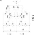
- FIG. 2 is a schematic circuit diagram illustrating the power converter of the present disclosure in the first operation mode.
- the first relay RY1 switches to connect the first inductor L1 to the first terminal of the first load capacitor C3
- the second relay RY2 switches to connect the second inductor L2 to the second terminal of the second load capacitor C4.
- the first switch S1 and the fourth switch S4 are turned on so that energy stored in the first bus capacitor C1 and the second bus capacitor C2 is transmitted to be stored in the first inductor L1 and the second inductor L2 (through a first energy storage path PS1 shown in the figure).
- the first switch S1 and the fourth switch S4 are turned off so that the energy stored in the first inductor L1 and the second inductor L2 is released to the first load capacitor C3 and the second load capacitor C4 (through a first energy release path PR1 shown in the figure).
- the power converter 1 transfers energy from the first bus capacitor C1 and the second bus capacitor C2 to the first load capacitor C3 and the second load capacitor C4, thereby realizing a DC-DC conversion (step-down) function.
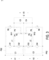
- FIG. 3 is a schematic circuit diagram illustrating the power converter of the present disclosure in the second operation mode.
- the first relay RY1 switches to connect the first inductor L1 to the second terminal of the fifth switch S5
- the second relay RY2 switches to connect the second inductor L2 to the first terminal of the sixth switch S6.
- the second switch S2, the third switch S3, and the fifth switch S5 are turned on so that energy stored in the first bus capacitor C1 is transmitted to be stored in the first inductor L1 and the second inductor L2 (through a second energy storage path PS2 shown in the figure).
- the power converter 1 transfers energy from the first bus capacitor C1 to the second bus capacitor C2, thereby adjusting the energy stored in the first bus capacitor C1 and the second bus capacitor C2 to realize the balance of bus capacitor voltages.
- FIG. 4 is a schematic circuit diagram illustrating the power converter of the present disclosure in the third operation mode.
- the first relay RY1 switches to connect the first inductor L1 to the second terminal of the fifth switch S5
- the second relay RY2 switches to connect the second inductor L2 to the first terminal of the sixth switch S6.
- the second switch S2, the third switch S3, and the sixth switch S6 are turned on so that energy stored in the second bus capacitor C2 is transmitted to be stored in the first inductor L1 and the second inductor L2 (through a third energy storage path PS3 shown in the figure).
- the power converter 1 transfers energy from the second bus capacitor C2 to the first bus capacitor C1, thereby adjusting the energy stored in the first bus capacitor C1 and the second bus capacitor C2 to realize the balance of bus capacitor voltages.
- FIGs. 5A and 5B are schematic circuit diagrams illustrating the power converter of the present disclosure in the fourth operation mode.
- the first relay RY1 switches to connect the first inductor L1 to the first terminal of the first load capacitor C3, and the second relay RY2 switches to connect the second inductor L2 to the first terminal of the sixth switch S6.
- the first switch S1, the third switch S3, and the sixth switch S6 are turned on.
- the power converter 1 transfers energy from the first bus capacitor C1 to the first load capacitor C3 and transfers energy from the second bus capacitor C2 to the first bus capacitor C1, thereby realizing the hybrid power supply.
- FIGs. 6A and 6B are schematic circuit diagrams illustrating the power converter of the present disclosure in the fifth operation mode.
- the first relay RY1 switches to connect the first inductor L1 to the second terminal of the fifth switch S5
- the second relay RY2 switches to connect the second inductor L2 to the second terminal of the second load capacitor C4.
- the second switch S2, the fourth switch S4, and the fifth switch S5 are turned on.
- the power converter 1 transfers energy from the first bus capacitor C1 to the second bus capacitor C2 and transfers energy from the second bus capacitor C2 to the second load capacitor C4, thereby realizing hybrid power supply.
- FIG. 7 is a schematic circuit diagram illustrating a power converter according to a second embodiment of the present disclosure.
- the power converter of the second embodiment shown in FIG. 7 further includes a power factor correction converter (PFC) 3.
- PFC power factor correction converter
- the first upper-bridge voltage conversion module 11, the first lower-bridge voltage conversion module 12, the second upper-bridge voltage conversion module 13, and the second lower-bridge voltage conversion module 14 form a buck converter
- the power source 2 is an AC power source
- the power factor correction converter 3 is connected between the power source 2 and the buck converter.
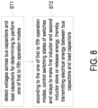
- FIG. 8 is a schematic flow chart illustrating a power conversion method according to an embodiment of the present disclosure.
- the power conversion method is applicable to the power converter of any of the foregoing embodiments.
- the power conversion method includes steps ST1 and ST2. Firstly, in the step ST1, voltages across the first bus capacitor C1, the second bus capacitor C2, the first load capacitor C3, and the second load capacitor C4 are detected for determining to perform one of the first operation mode, the second operation mode, the third operation mode, the fourth operation mode, and the fifth operation mode.
- step ST2 according to the one of the first to fifth operation modes, switching states of the first switch S1, the second switch S2, the third switch S3, the fourth switch S4, the fifth switch S5, the sixth switch S6, the first relay RY1, and the second relay RY2 are controlled to make the first inductor L1 and the second inductor L2 store or release energy, thereby transmitting electrical energy between the first bus capacitor C1, the second bus capacitor C2, the first load capacitor C3, and the second load capacitor C4.
- the power conversion method includes following steps. Firstly, switch the first relay RY1 to connect the first inductor L1 to the first terminal of the first load capacitor C3, and switch the second relay RY2 to connect the second inductor L2 to the second terminal of the second load capacitor C4. Then, turn on the first switch S1 and the fourth switch S4 for transmitting the energy stored in the first bus capacitor C1 and the second bus capacitor C2 to be stored in the first inductor L1 and the second inductor L2. Finally, turn off the first switch S 1 and the fourth switch S4 for releasing the energy stored in the first inductor L1 and the second inductor L2 to the first load capacitor C3 and the second load capacitor C4.
- the power conversion method includes following steps. Firstly, switch the first relay RY1 to connect the first inductor L1 to the second terminal of the fifth switch S5, and switch the second relay RY2 to connect the second inductor L2 to the first terminal of the sixth switch S6. Then, turn on the second switch S2, the third switch S3, and the fifth switch S5 for transmitting the energy stored in the first bus capacitor C1 to be stored in the first inductor L1 and the second inductor L2. Finally, turn on the second switch S2 and the third switch S3 and turn off the fifth switch S5 for releasing the energy stored in the first inductor L1 and the second inductor L2 to the second bus capacitor C2.
- the power conversion method includes following steps. Firstly, switch the first relay RY1 to connect the first inductor L1 to the second terminal of the fifth switch S5, and switch the second relay RY2 to connect the second inductor L2 to the first terminal of the sixth switch S6. Then, turn on the second switch S2, the third switch S3, and the sixth switch S6 for transmitting the energy stored in the second bus capacitor C2 to be stored in the first inductor L1 and the second inductor L2. Finally, turn on the second switch S2 and the third switch S3 and turn off the sixth switch S6 for releasing the energy stored in the first inductor L1 and the second inductor L2 to the first bus capacitor C 1.
- the power conversion method includes following steps. Firstly, switch the first relay RY1 to connect the first inductor L1 to the first terminal of the first load capacitor C3, and switch the second relay RY2 to connect the second inductor L2 to the first terminal of the sixth switch S6. Then, turn on the first switch S1, the third switch S3, and the sixth switch S6 for transmitting the energy stored in the first bus capacitor C1 to be stored in the first inductor L1 and transmitting the energy stored in the second bus capacitor C2 to be stored in the second inductor L2.
- the power conversion method includes following steps. Firstly, switch the first relay RY1 to connect the first inductor L1 to the second terminal of the fifth switch S5, and switch the second relay RY2 to connect the second inductor L2 to the second terminal of the second load capacitor C4. Then, turn on the second switch S2, the fourth switch S4, and the fifth switch S5 for transmitting the energy stored in the first bus capacitor C1 to be stored in the first inductor L1 and transmitting the energy stored in the second bus capacitor C2 to be stored in the second inductor L2.
- the present disclosure provides a power converter and a power conversion method which realize a balance of capacitor voltages based on inherent inductor components of converter.
- the power converter and the power conversion method of the present disclosure can reduce a size of overall circuit and improve a power density.
- the power converter and the power conversion method of the present disclosure are able to realize energy balance and hybrid power supply and satisfy various load requirements.
Landscapes
- Engineering & Computer Science (AREA)
- Power Engineering (AREA)
- Dc-Dc Converters (AREA)
- Inverter Devices (AREA)
Abstract
A power converter (1) and a power conversion method are provided and capable of bus capacitor voltage balance based on inherent inductor components of the power converter. Compared with the conventional approach that adds a balance circuit, the power converter (1) and the power conversion method can reduce a size of overall circuit and improve a power density. In addition, two relays (RY1, RY2) of the power converter (1) are configured to switch switching states such that two inductors (L1, L2) store or release energy, thereby transmitting electrical energy between two bus capacitors (C1, C2) and two load capacitors (C3, C4). The power converter (1) and the power conversion method are able to realize energy balance and hybrid power supply and satisfy various load requirements.
Description
- The present disclosure relates to a power converter and a power conversion method, and more particularly to a power converter and a power conversion method capable of realizing energy balance and hybrid power supply.
- In a DC/DC converter with two bus capacitors, the two bus capacitors are connected between a positive input terminal and a negative input terminal, and thus an input side has a positive bus capacitor voltage and a negative bus capacitor voltage. When the DC/DC converter performs voltage reduction and supplies power to an output side, an imbalance between the positive and negative bus capacitor voltages may be caused by different duty cycles of switches within the DC-DC converter.
- To balance the positive and negative bus capacitor voltages, conventional approaches usually add a balance circuit to adjust the bus capacitor voltages. However, the additional balance circuit increases a size of overall circuit and thus reduces a power density.
- Therefore, there is a need of providing a power converter and a power conversion method in order to overcome the drawbacks of the conventional technologies.
- The present disclosure provides a power converter and a power conversion method which realize a balance of capacitor voltages based on inherent inductor components of converter. Compared with the conventional approach that adds a balance circuit, the power converter and the power conversion method of the present disclosure can reduce a size of overall circuit and improve a power density. In addition, through transmitting electrical energy between capacitors and inductors, the power converter and the power conversion method of the present disclosure are able to realize energy balance and hybrid power supply and satisfy various load requirements.
- In accordance with an aspect of the present disclosure, a power converter is provided. The power converter includes a first upper-bridge voltage conversion module, a first lower-bridge voltage conversion module, a second upper-bridge voltage conversion module, and a second lower-bridge voltage conversion module. The first upper-bridge voltage conversion module includes a first bus capacitor, a first switch, a second switch, a first inductor and a first load capacitor, and the first switch, the second switch and the first inductor are electrically connected between the first bus capacitor and the first load capacitor. The first lower-bridge voltage conversion module includes a second bus capacitor, a third switch, a fourth switch, a second inductor and a second load capacitor, and the third switch, the fourth switch and the second inductor are electrically connected between the second bus capacitor and the second load capacitor. The second upper-bridge voltage conversion module includes a fifth switch and a first relay. A first terminal of the fifth switch is connected to a first terminal of the first bus capacitor, the first relay is configured to selectively switch to connect the first inductor to a second terminal of the fifth switch or a first terminal of the first load capacitor, and a second terminal of the first load capacitor is connected to a second terminal of the first bus capacitor. The second lower-bridge voltage conversion module includes a sixth switch and a second relay. A first terminal of the second load capacitor is connected to a first terminal of the second bus capacitor, the second relay is configured to selectively switch to connect the second inductor to a first terminal of the sixth switch or a second terminal of the second load capacitor, and a second terminal of the sixth switch is connected to a second terminal of the second bus capacitor. The first switch, the second switch, the third switch, the fourth switch, the fifth switch, the sixth switch, the first relay and the second relay are configured to switch switching states for making the first inductor and the second inductor store or release energy, thereby transmitting electrical energy between the first bus capacitor, the second bus capacitor, the first load capacitor and the second load capacitor.
- In accordance with another aspect of the present disclosure, a power conversion method is provided. The power conversion method is applied to the power converter of the present disclosure and includes steps of: detecting voltages across the first bus capacitor, the second bus capacitor, the first load capacitor and the second load capacitor for determining to perform one of a first operation mode, a second operation mode, a third operation mode, a fourth operation mode and a fifth operation mode; and according to the one of the first to fifth operation modes, controlling switching states of the first switch, the second switch, the third switch, the fourth switch, the fifth switch, the sixth switch, the first relay and the second relay to make the first inductor and the second inductor store or release energy, thereby transmitting electrical energy between the first bus capacitor, the second bus capacitor, the first load capacitor and the second load capacitor.
-
-
FIG. 1 is a schematic circuit diagram illustrating a power converter according to a first embodiment of the present disclosure; -
FIG. 2 is a schematic circuit diagram illustrating the power converter of the present disclosure in the first operation mode; -
FIG. 3 is a schematic circuit diagram illustrating the power converter of the present disclosure in the second operation mode; -
FIG. 4 is a schematic circuit diagram illustrating the power converter of the present disclosure in the third operation mode; -
FIGs. 5A and5B are schematic circuit diagrams illustrating the power converter of the present disclosure in the fourth operation mode; -
FIGs. 6A and6B are schematic circuit diagrams illustrating the power converter of the present disclosure in the fifth operation mode; -
FIG. 7 is a schematic circuit diagram illustrating a power converter according to a second embodiment of the present disclosure; and -
FIG. 8 is a schematic flow chart illustrating a power conversion method according to an embodiment of the present disclosure. - The present disclosure will now be described more specifically with reference to the following embodiments. It is to be noted that the following descriptions of preferred embodiments of this disclosure are presented herein for purpose of illustration and description only.
-
FIG. 1 is a schematic circuit diagram illustrating a power converter according to a first embodiment of the present disclosure. As shown inFIG. 1 , thepower converter 1 includes a first upper-bridgevoltage conversion module 11, a first lower-bridgevoltage conversion module 12, a second upper-bridgevoltage conversion module 13, and a second lower-bridgevoltage conversion module 14. - The first upper-bridge
voltage conversion module 11 includes a first bus capacitor C1, a first switch S1, a second switch S2, a first inductor L1, and a first load capacitor C3. The first switch S1, the second switch S2, and the first inductor L1 are electrically connected between the first bus capacitor C1 and the first load capacitor C3. The first lower-bridgevoltage conversion module 12 includes a second bus capacitor C2, a third switch S3, a fourth switch S4, a second inductor L2, and a second load capacitor C4. The third switch S3, the fourth switch S4, and the second inductor L2 are electrically connected between the second bus capacitor C2 and the second load capacitor C4. - The second upper-bridge
voltage conversion module 13 includes a fifth switch S5 and a first relay RY1. A first terminal of the fifth switch S5 is connected to a first terminal of the first bus capacitor C1. The first relay RY1 is configured to selectively switch to connect the first inductor L1 to a second terminal of the fifth switch S5 or a first terminal of the first load capacitor C3. A second terminal of the first load capacitor C3 is connected to a second terminal of the first bus capacitor C1. In this embodiment, the first relay RY1 includes a first moving contact P1, a first static contact P2, and a second static contact P3 respectively connected to the first inductor L1, the second terminal of the fifth switch S5, and the first terminal of the first load capacitor C3. When the first relay RY1 switches the first moving contact P1 to connect to the first static contact P2, the first inductor L1 is connected to the second terminal of the fifth switch S5. When the first relay RY1 switches the first moving contact P1 to connect to the second static contact P3, the first inductor L1 is connected to the first terminal of the first load capacitor C3. - The second lower-bridge
voltage conversion module 14 includes a sixth switch S6 and a second relay RY2. A first terminal of the second load capacitor C4 is connected to a first terminal of the second bus capacitor C2. The second relay RY2 is configured to selectively switch to connect the second inductor L2 to a first terminal of the sixth switch S6 or a second terminal of the second load capacitor C4. A second terminal of the sixth switch S6 is connected to a second terminal of the second bus capacitor C2. In this embodiment, the second relay RY2 includes a second moving contact P4, a third static contact P5, and a fourth static contact P6 respectively connected to the second inductor L2, the first terminal of the sixth switch S6, and the second terminal of the second load capacitor C4. When the second relay RY2 switches the second moving contact P4 to connect to the third static contact P5, the second inductor L2 is connected to the first terminal of the sixth switch S6. When the second relay RY2 switches the second moving contact P4 to connect to the fourth static contact P6, the second inductor L2 is connected to the second terminal of the second load capacitor C4. Further, the second terminal of the fifth switch S5 and the first terminal of the sixth switch S6 are connected to each other.FIG. 1 exemplifies the first to sixth switches S1-S6 as IGBTs (insulated gate bipolar transistors), but the possible implementations of these switches are not limited thereto. For example, the first to sixth switches S1-S6 may be MOSFETs (metal-oxide-semiconductor field effect transistors). - The first switch S1, the second switch S2, the third switch S3, the fourth switch S4, the fifth switch S5, the sixth switch S6, the first relay RY1, and the second relay RY2 are configured to switch their switching states such that the first inductor L1 and the second inductor L2 store or release energy. Thereby, electrical energy is transmitted between the first bus capacitor C1, the second bus capacitor C2, the first load capacitor C3, and the second load capacitor C4. Consequently, voltage balance of the capacitors is achieved based on inherent inductor components of converter. Compared with the conventional approach that adds a balance circuit, the power converter and the power conversion method of the present disclosure can reduce the size of overall circuit and improve the power density. In addition, through transmitting electrical energy between capacitors and inductors, the power converter and the power conversion method of the present disclosure is able to realize energy balance and hybrid power supply and satisfy various load requirements.
- Additionally, the first bus capacitor C1 is configured to establish a first voltage V1, the second bus capacitor C2 is configured to establish a second voltage V2, and the first load capacitor C3 and the second load capacitor C4 are configured to establish a third voltage V3. In the embodiment shown in
FIG. 1 , the first voltage V1 and the second voltage V2 serves as input-side voltages, and the third voltage V3 serves as an output-side voltage. Under this circumstance, thepower converter 1 may further include apower source 2 and a load (e.g., a capacitor C shown inFIG. 1 ), and thepower source 2 is connected to a positive input terminal Bus+, a neutral terminal N, and a negative input terminal Bus- of thepower converter 1. The positive input terminal Bus+ is connected to the first terminal of the first bus capacitor C1, the negative input terminal Bus- is connected to the second terminal of the second bus capacitor C2, and the load (the capacitor C) is connected to the first terminal of the first load capacitor C3 and the second terminal of the second load capacitor C4. The neutral terminal N is connected to the second terminal of the first bus capacitor C1, the first terminal of the second bus capacitor C2, the second terminal of the first load capacitor C3, the first terminal of the second load capacitor C4, a second terminal of the second switch S2, and a first terminal of the third switch S3. In fact, thepower converter 1 of the present disclosure is a bidirectional power converter. Specifically, in another embodiment, the third voltage V3 may serve as an input-side voltage, and correspondingly the first voltage V1 and the second voltage V2 may serve as output-side voltages. In this case, the positions of thepower source 2 and the load are interchanged, the specific operation thereof can be derived from the embodiment shown inFIG. 1 , and thus detailed descriptions thereof are omitted herein. - In an embodiment, as shown in
FIG. 1 , first and second terminals of the first switch S1 are connected to the first terminal of the first bus capacitor C1 and a first terminal of the second switch S2 respectively, and the second terminal of the second switch S2 is connected to the second terminal of the first bus capacitor C1. A first terminal of the first inductor L1 is connected to the second terminal of the first switch S1 and the first terminal of the second switch S2, and a second terminal of the first inductor L1 is connected to the first relay RY1. - In an embodiment, as shown in
FIG. 1 , the first terminal and a second terminal of the third switch S3 are connected to the first terminal of the second bus capacitor C2 and a first terminal of the fourth switch S4 respectively, and a second terminal of the fourth switch S4 is connected to the second terminal of the second bus capacitor C2. A first terminal of the second inductor L2 is connected to the second terminal of the third switch S3 and the first terminal of the fourth switch S4, and a second terminal of the second inductor L2 is connected to the second relay RY2. - In an embodiment, the
power converter 1 is controlled by a controller (not shown), such as a digital signal processor, a programmable logic controller, or a microcontroller. The controller is configured to detect a variation rate of voltages across the capacitors and determines one of the first to fifth operation modes that thepower converter 1 performs accordingly, thereby achieving the energy balance and hybrid power supply. In another embodiment, the controller receives a user command to control thepower converter 1 to perform a specific operation mode for energy dispatching. - Please refer to
FIG. 2. FIG. 2 is a schematic circuit diagram illustrating the power converter of the present disclosure in the first operation mode. As shown inFIG. 2 , in the first operation mode, the first relay RY1 switches to connect the first inductor L1 to the first terminal of the first load capacitor C3, and the second relay RY2 switches to connect the second inductor L2 to the second terminal of the second load capacitor C4. Firstly, the first switch S1 and the fourth switch S4 are turned on so that energy stored in the first bus capacitor C1 and the second bus capacitor C2 is transmitted to be stored in the first inductor L1 and the second inductor L2 (through a first energy storage path PS1 shown in the figure). Then, the first switch S1 and the fourth switch S4 are turned off so that the energy stored in the first inductor L1 and the second inductor L2 is released to the first load capacitor C3 and the second load capacitor C4 (through a first energy release path PR1 shown in the figure). In the first operation mode, thepower converter 1 transfers energy from the first bus capacitor C1 and the second bus capacitor C2 to the first load capacitor C3 and the second load capacitor C4, thereby realizing a DC-DC conversion (step-down) function. - Please refer to
FIG. 3. FIG. 3 is a schematic circuit diagram illustrating the power converter of the present disclosure in the second operation mode. As shown inFIG. 3 , in the second operation mode, the first relay RY1 switches to connect the first inductor L1 to the second terminal of the fifth switch S5, and the second relay RY2 switches to connect the second inductor L2 to the first terminal of the sixth switch S6. Firstly, the second switch S2, the third switch S3, and the fifth switch S5 are turned on so that energy stored in the first bus capacitor C1 is transmitted to be stored in the first inductor L1 and the second inductor L2 (through a second energy storage path PS2 shown in the figure). Then, the second switch S2 and the third switch S3 are turned on and the fifth switch S5 is turned off so that the energy stored in the first inductor L1 and the second inductor L2 is released to the second bus capacitor C2 (through a second energy release path PR2 shown in the figure). In the second operation mode, thepower converter 1 transfers energy from the first bus capacitor C1 to the second bus capacitor C2, thereby adjusting the energy stored in the first bus capacitor C1 and the second bus capacitor C2 to realize the balance of bus capacitor voltages. - Please refer to
FIG. 4. FIG. 4 is a schematic circuit diagram illustrating the power converter of the present disclosure in the third operation mode. As shown inFIG. 4 , in the third operation mode, the first relay RY1 switches to connect the first inductor L1 to the second terminal of the fifth switch S5, and the second relay RY2 switches to connect the second inductor L2 to the first terminal of the sixth switch S6. Firstly, the second switch S2, the third switch S3, and the sixth switch S6 are turned on so that energy stored in the second bus capacitor C2 is transmitted to be stored in the first inductor L1 and the second inductor L2 (through a third energy storage path PS3 shown in the figure). Then, the second switch S2 and the third switch S3 are turned on and the sixth switch S6 is turned off so that the energy stored in the first inductor L1 and the second inductor L2 is released to the first bus capacitor C1 (through a third energy release path PR3 shown in the figure). In the third operation mode, thepower converter 1 transfers energy from the second bus capacitor C2 to the first bus capacitor C1, thereby adjusting the energy stored in the first bus capacitor C1 and the second bus capacitor C2 to realize the balance of bus capacitor voltages. - Please refer to
FIGs. 5A and5B .FIGs. 5A and5B are schematic circuit diagrams illustrating the power converter of the present disclosure in the fourth operation mode. As shown inFIGs. 5A and5B , in the fourth operation mode, the first relay RY1 switches to connect the first inductor L1 to the first terminal of the first load capacitor C3, and the second relay RY2 switches to connect the second inductor L2 to the first terminal of the sixth switch S6. Firstly, as shown inFIG. 5A , the first switch S1, the third switch S3, and the sixth switch S6 are turned on. Accordingly, energy stored in the first bus capacitor C1 is transmitted to be stored in the first inductor L1 (through a fourth energy storage path PS4 shown in the figure), and energy stored in the second bus capacitor C2 is transmitted to be stored in the second inductor L2 (through a fifth energy storage path PS5 shown in the figure). Then, as shown inFIG. 5B , the third switch S3 is turned on, and the first switch S1 and the sixth switch S6 are turned off. Accordingly, the energy stored in the first inductor L1 is released to the first load capacitor C3 (through a fourth energy release path PR4 shown in the figure), and the energy stored in the second inductor L2 is released to the first bus capacitor C1 (through a fifth energy release path PR5 shown in the figure). In the fourth operation mode, thepower converter 1 transfers energy from the first bus capacitor C1 to the first load capacitor C3 and transfers energy from the second bus capacitor C2 to the first bus capacitor C1, thereby realizing the hybrid power supply. - Please refer to
FIGs. 6A and6B .FIGs. 6A and6B are schematic circuit diagrams illustrating the power converter of the present disclosure in the fifth operation mode. As shown inFIGs. 6A and6B , in the fifth operation mode, the first relay RY1 switches to connect the first inductor L1 to the second terminal of the fifth switch S5, and the second relay RY2 switches to connect the second inductor L2 to the second terminal of the second load capacitor C4. Firstly, as shown inFIG. 6A , the second switch S2, the fourth switch S4, and the fifth switch S5 are turned on. Accordingly, energy stored in the first bus capacitor C1 is transmitted to be stored in the first inductor L1 (through a sixth energy storage path PS6 shown in the figure), and energy stored in the second bus capacitor C2 is transmitted to be stored in the second inductor L2 (through a seventh energy storage path PS7 shown in the figure). Then, as shown inFIG. 6B , the second switch S2 is turned on, and the fourth switch S4 and the fifth switch S5 are turned off. Accordingly, the energy stored in the first inductor L1 is released to the second bus capacitor C2 (through a sixth energy release path PR6 shown in the figure), and the energy stored in the second inductor L2 is released to the second load capacitor C4 (through a seventh energy release path PR7 shown in the figure). In the fifth operation mode, thepower converter 1 transfers energy from the first bus capacitor C1 to the second bus capacitor C2 and transfers energy from the second bus capacitor C2 to the second load capacitor C4, thereby realizing hybrid power supply. - Please refer to
FIG. 7. FIG. 7 is a schematic circuit diagram illustrating a power converter according to a second embodiment of the present disclosure. Different from the first embodiment shown inFIG. 1 , the power converter of the second embodiment shown inFIG. 7 further includes a power factor correction converter (PFC) 3. In the second embodiment, as shown inFIG. 7 , the first upper-bridgevoltage conversion module 11, the first lower-bridgevoltage conversion module 12, the second upper-bridgevoltage conversion module 13, and the second lower-bridgevoltage conversion module 14 form a buck converter, thepower source 2 is an AC power source, and the powerfactor correction converter 3 is connected between thepower source 2 and the buck converter. - Please refer to
FIG. 8. FIG. 8 is a schematic flow chart illustrating a power conversion method according to an embodiment of the present disclosure. The power conversion method is applicable to the power converter of any of the foregoing embodiments. As shown inFIG. 8 , the power conversion method includes steps ST1 and ST2. Firstly, in the step ST1, voltages across the first bus capacitor C1, the second bus capacitor C2, the first load capacitor C3, and the second load capacitor C4 are detected for determining to perform one of the first operation mode, the second operation mode, the third operation mode, the fourth operation mode, and the fifth operation mode. Then, in the step ST2, according to the one of the first to fifth operation modes, switching states of the first switch S1, the second switch S2, the third switch S3, the fourth switch S4, the fifth switch S5, the sixth switch S6, the first relay RY1, and the second relay RY2 are controlled to make the first inductor L1 and the second inductor L2 store or release energy, thereby transmitting electrical energy between the first bus capacitor C1, the second bus capacitor C2, the first load capacitor C3, and the second load capacitor C4. - In the first operation mode, the power conversion method includes following steps. Firstly, switch the first relay RY1 to connect the first inductor L1 to the first terminal of the first load capacitor C3, and switch the second relay RY2 to connect the second inductor L2 to the second terminal of the second load capacitor C4. Then, turn on the first switch S1 and the fourth switch S4 for transmitting the energy stored in the first bus capacitor C1 and the second bus capacitor C2 to be stored in the first inductor L1 and the second inductor L2. Finally, turn off the
first switch S 1 and the fourth switch S4 for releasing the energy stored in the first inductor L1 and the second inductor L2 to the first load capacitor C3 and the second load capacitor C4. - In the second operation mode, the power conversion method includes following steps. Firstly, switch the first relay RY1 to connect the first inductor L1 to the second terminal of the fifth switch S5, and switch the second relay RY2 to connect the second inductor L2 to the first terminal of the sixth switch S6. Then, turn on the second switch S2, the third switch S3, and the fifth switch S5 for transmitting the energy stored in the first bus capacitor C1 to be stored in the first inductor L1 and the second inductor L2. Finally, turn on the second switch S2 and the third switch S3 and turn off the fifth switch S5 for releasing the energy stored in the first inductor L1 and the second inductor L2 to the second bus capacitor C2.
- In the third operation mode, the power conversion method includes following steps. Firstly, switch the first relay RY1 to connect the first inductor L1 to the second terminal of the fifth switch S5, and switch the second relay RY2 to connect the second inductor L2 to the first terminal of the sixth switch S6. Then, turn on the second switch S2, the third switch S3, and the sixth switch S6 for transmitting the energy stored in the second bus capacitor C2 to be stored in the first inductor L1 and the second inductor L2. Finally, turn on the second switch S2 and the third switch S3 and turn off the sixth switch S6 for releasing the energy stored in the first inductor L1 and the second inductor L2 to the first
bus capacitor C 1. - In the fourth operation mode, the power conversion method includes following steps. Firstly, switch the first relay RY1 to connect the first inductor L1 to the first terminal of the first load capacitor C3, and switch the second relay RY2 to connect the second inductor L2 to the first terminal of the sixth switch S6. Then, turn on the first switch S1, the third switch S3, and the sixth switch S6 for transmitting the energy stored in the first bus capacitor C1 to be stored in the first inductor L1 and transmitting the energy stored in the second bus capacitor C2 to be stored in the second inductor L2. Finally, turn on the third switch S3 and turn off the
first switch S 1 and the sixth switch S6 for releasing the energy stored in the first inductor L1 to the first load capacitor C3 and releasing the energy stored in the second inductor L2 to the firstbus capacitor C 1. - In the fifth operation mode, the power conversion method includes following steps. Firstly, switch the first relay RY1 to connect the first inductor L1 to the second terminal of the fifth switch S5, and switch the second relay RY2 to connect the second inductor L2 to the second terminal of the second load capacitor C4. Then, turn on the second switch S2, the fourth switch S4, and the fifth switch S5 for transmitting the energy stored in the first bus capacitor C1 to be stored in the first inductor L1 and transmitting the energy stored in the second bus capacitor C2 to be stored in the second inductor L2. Finally, turn on the second switch S2 and turn off the fourth switch S4 and the fifth switch S5 for releasing the energy stored in the first inductor L1 to the second bus capacitor C2 and releasing the energy stored in the second inductor L2 to the second load capacitor C4.
- In summary, the present disclosure provides a power converter and a power conversion method which realize a balance of capacitor voltages based on inherent inductor components of converter. Compared with the conventional approach that adds a balance circuit, the power converter and the power conversion method of the present disclosure can reduce a size of overall circuit and improve a power density. In addition, through transmitting electrical energy between capacitors and inductors, the power converter and the power conversion method of the present disclosure are able to realize energy balance and hybrid power supply and satisfy various load requirements.
Claims (15)
- A power converter (1), characterized by comprising:a first upper-bridge voltage conversion module (11) comprising a first bus capacitor (C1), a first switch (S1), a second switch (S2), a first inductor (L1) and a first load capacitor (C3), wherein the first switch (S1), the second switch (S2) and the first inductor (L1) are electrically connected between the first bus capacitor (C1) and the first load capacitor (C3);a first lower-bridge voltage conversion module (12) comprising a second bus capacitor (C2), a third switch (S3), a fourth switch (S4), a second inductor (L2) and a second load capacitor (C4), wherein the third switch (S3), the fourth switch (S4) and the second inductor (L2) are electrically connected between the second bus capacitor (C2) and the second load capacitor (C4);a second upper-bridge voltage conversion module (13) comprising a fifth switch (S5) and a first relay (RY1), wherein a first terminal of the fifth switch (S5) is connected to a first terminal of the first bus capacitor (C1), the first relay (RY1) is configured to selectively switch to connect the first inductor (L1) to a second terminal of the fifth switch (S5) or a first terminal of the first load capacitor (C3), and a second terminal of the first load capacitor (C3) is connected to a second terminal of the first bus capacitor (C1); anda second lower-bridge voltage conversion module (14) comprising a sixth switch (S6) and a second relay (RY2), wherein a first terminal of the second load capacitor (C4) is connected to a first terminal of the second bus capacitor (C2), the second relay (RY2) is configured to selectively switch to connect the second inductor (L2) to a first terminal of the sixth switch (S6) or a second terminal of the second load capacitor (C4), and a second terminal of the sixth switch (S6) is connected to a second terminal of the second bus capacitor (C2),wherein the first switch (S1), the second switch (S2), the third switch (S3), the fourth switch (S4), the fifth switch (S5), the sixth switch (S6), the first relay (RY1) and the second relay (RY2) are configured to switch switching states such that the first inductor (L1) and the second inductor (L2) store or release energy, thereby transmitting electrical energy between the first bus capacitor (C1), the second bus capacitor (C2), the first load capacitor (C3) and the second load capacitor (C4).
- The power converter (1) according to claim 1, wherein the first relay (RY1) comprises a first moving contact (P1), a first static contact (P2) and a second static contact (P3) respectively connected to the first inductor (L1), the second terminal of the fifth switch (S5) and the first terminal of the first load capacitor (C3); when the first relay (RY1) switches the first moving contact (P1) to connect to the first static contact (P2), the first inductor (L1) is connected to the second terminal of the fifth switch (S5); and when the first relay (RY1) switches the first moving contact (P1) to connect to the second static contact (P3), the first inductor (L1) is connected to the first terminal of the first load capacitor (C3).
- The power converter (1) according to claim 1, wherein the second relay (RY2) comprises a second moving contact (P4), a third static contact (P5) and a fourth static contact (P6) respectively connected to the second inductor (L2), the first terminal of the sixth switch (S6) and the second terminal of the second load capacitor (C4); when the second relay (RY2) switches the second moving contact (P4) to connect to the third static contact (P5), the second inductor (L2) is connected to the first terminal of the sixth switch (S6); and when the second relay (RY2) switches the second moving contact (P4) to connect to the fourth static contact (P6), the second inductor (L2) is connected to the second terminal of the second load capacitor (C4).
- The power converter (1) according to claim 1, wherein the second terminal of the fifth switch (S5) and the first terminal of the sixth switch (S6) are connected to each other.
- The power converter (1) according to claim 1, wherein a first terminal and a second terminal of the first switch (S 1) are respectively connected to the first terminal of the first bus capacitor (C1) and a first terminal of the second switch (S2), a second terminal of the second switch (S2) is connected to the second terminal of the first bus capacitor (C1), a first terminal of the first inductor (L1) is connected to the second terminal of the first switch (S1) and the first terminal of the second switch (S2), and a second terminal of the first inductor (L1) is connected to the first relay (RY1).
- The power converter (1) according to claim 1, wherein a first terminal and a second terminal of the third switch (S3) are respectively connected to the first terminal of the second bus capacitor (C2) and a first terminal of the fourth switch (S4), a second terminal of the fourth switch (S4) is connected to the second terminal of the second bus capacitor (C2), a first terminal of the second inductor (L2) is connected to the second terminal of the third switch (S3) and the first terminal of the fourth switch (S4), and a second terminal of the second inductor (L2) is connected to the second relay (RY2).
- The power converter (1) according to claim 1, wherein the first bus capacitor (C1) is configured to establish a first voltage (V1), the second bus capacitor (C2) is configured to establish a second voltage (V2), and the first load capacitor (C3) and the second load capacitor are configured to establish a third voltage (V3).
- The power converter (1) according to claim 1, further comprising a neutral terminal (N), a power source (2) and a load (C), wherein the power source (2) is connected to the first and second terminals of the first bus capacitor (C1) and the first and second terminals of the second bus capacitor (C2), the load is connected to the first terminal of the first load capacitor (C3) and the second terminal of the second load capacitor (C4), the neutral terminal (N) is connected to the second terminal of the first bus capacitor (C1), the first terminal of the second bus capacitor (C2), the second terminal of the first load capacitor (C3), the first terminal of the second load capacitor (C4), a second terminal of the second switch (S2) and a first terminal of the third switch (S3).
- The power converter (1) according to claim 1, further comprising a power source (2) and a power factor correction converter (3), wherein the first upper-bridge voltage conversion module (11), the first lower-bridge voltage conversion module (12), the second upper-bridge voltage conversion module (13) and the second lower-bridge voltage conversion module (14) form a buck converter, and the power factor correction converter (3) is connected between the power source (2) and the buck converter.
- A power conversion method applied to the power converter (1) as claimed in claim 1, and the power conversion method characterized by comprising steps of:detecting voltages across the first bus capacitor (C1), the second bus capacitor (C2), the first load capacitor (C3) and the second load capacitor (C4) for determining to perform one of a first operation mode, a second operation mode, a third operation mode, a fourth operation mode and a fifth operation mode; andaccording to the one of the first to fifth operation modes, controlling switching states of the first switch (S1), the second switch (S2), the third switch (S3), the fourth switch (S4), the fifth switch (S5), the sixth switch (S6), the first relay (RY1) and the second relay (RY2) to make the first inductor (L1) and the second inductor (L2) store or release energy, thereby transmitting electrical energy between the first bus capacitor (C1), the second bus capacitor (C2), the first load capacitor (C3) and the second load capacitor (C4).
- The power conversion method according to claim 10, wherein in the first operation mode, the power conversion method comprises steps of:switching the first relay (RY1) to connect the first inductor (L1) to the first terminal of the first load capacitor (C3), and switching the second relay (RY2) to connect the second inductor (L2) to the second terminal of the second load capacitor (C4);turning on the first switch (S1) and the fourth switch (S4) for transmitting energy stored in the first bus capacitor (C1) and the second bus capacitor (C2) to be stored in the first inductor (L1) and the second inductor (L2); andturning off the first switch (S1) and the fourth switch (S4) for releasing energy stored in the first inductor (L1) and the second inductor (L2) to the first load capacitor (C3) and the second load capacitor (C4).
- The power conversion method according to claim 10, wherein in the second operation mode, the power conversion method comprises steps of:switching the first relay (RY1) to connect the first inductor (L1) to the second terminal of the fifth switch (S5), and switching the second relay (RY2) to connect the second inductor (L2) to the first terminal of the sixth switch (S6);turning on the second switch (S2), the third switch (S3) and the fifth switch (S5) for transmitting energy stored in the first bus capacitor (C1) to be stored in the first inductor (L1) and the second inductor (L2); andturning on the second switch (S2) and the third switch (S3) and turning off the fifth switch (S5) for releasing energy stored in the first inductor (L1) and the second inductor (L2) to the second bus capacitor (C2).
- The power conversion method according to claim 10, wherein in the third operation mode, the power conversion method comprises steps of:switching the first relay (RY1) to connect the first inductor (L1) to the second terminal of the fifth switch (S5), and switching the second relay (RY2) to connect the second inductor (L2) to the first terminal of the sixth switch (S6);turning on the second switch (S2), the third switch (S3) and the sixth switch (S6) for transmitting energy stored in the second bus capacitor (C2) to be stored in the first inductor (L1) and the second inductor (L2); andturning on the second switch (S2) and the third switch (S3) and turning off the sixth switch (S6) for releasing energy stored in the first inductor (L1) and the second inductor (L2) to the first bus capacitor (C1).
- The power conversion method according to claim 10, wherein in the fourth operation mode, the power conversion method comprises steps of:switching the first relay (RY1) to connect the first inductor (L1) to the first terminal of the first load capacitor (C3), and switching the second relay (RY2) to connect the second inductor (L2) to the first terminal of the sixth switch (S6);turning on the first switch (S1), the third switch (S3) and the sixth switch (S6) for transmitting energy stored in the first bus capacitor (C1) to be stored in the first inductor (L1) and transmitting energy stored in the second bus capacitor (C2) to be stored in the second inductor (L2); andturning on the third switch (S3) and turning off the first switch (S1) and the sixth switch (S6) for releasing energy stored in the first inductor (L1) to the first load capacitor (C3) and releasing energy stored in the second inductor (L2) to the first bus capacitor (C1).
- The power conversion method according to claim 10, wherein in the fifth operation mode, the power conversion method comprises steps of:switching the first relay (RY1) to connect the first inductor (L1) to the second terminal of the fifth switch (S5), and switching the second relay (RY2) to connect the second inductor (L2) to the second terminal of the second load capacitor (C4);turning on the second switch (S2), the fourth switch (S4) and the fifth switch (S5) for transmitting energy stored in the first bus capacitor (C1) to be stored in the first inductor (L1) and transmitting energy stored in the second bus capacitor (C2) to be stored in the second inductor (L2); andturning on the second switch (S2) and turning off the fourth switch (S4) and the fifth switch (S5) for releasing energy stored in the first inductor (L1) to the second bus capacitor (C2) and releasing energy stored in the second inductor (L2) to the second load capacitor (C4).
Applications Claiming Priority (1)
| Application Number | Priority Date | Filing Date | Title |
|---|---|---|---|
| CN202311274168.7A CN119727382A (en) | 2023-09-28 | 2023-09-28 | Power converter and power conversion method |
Publications (1)
| Publication Number | Publication Date |
|---|---|
| EP4531259A1 true EP4531259A1 (en) | 2025-04-02 |
Family
ID=89224242
Family Applications (1)
| Application Number | Title | Priority Date | Filing Date |
|---|---|---|---|
| EP23218060.4A Pending EP4531259A1 (en) | 2023-09-28 | 2023-12-19 | Power converter and power conversion method |
Country Status (3)
| Country | Link |
|---|---|
| US (1) | US12438464B2 (en) |
| EP (1) | EP4531259A1 (en) |
| CN (1) | CN119727382A (en) |
Citations (2)
| Publication number | Priority date | Publication date | Assignee | Title |
|---|---|---|---|---|
| US20150244268A1 (en) * | 2014-02-27 | 2015-08-27 | Edison DC Systems, Inc. | Power conversion system with controlled neutral |
| US20190273445A1 (en) * | 2016-10-26 | 2019-09-05 | Korea Electric Power Corporation | Apparatus for controlling output voltage for single-type converter, and method therefor |
Family Cites Families (12)
| Publication number | Priority date | Publication date | Assignee | Title |
|---|---|---|---|---|
| WO2007110954A1 (en) * | 2006-03-29 | 2007-10-04 | Mitsubishi Denki Kabushiki Kaisha | Power supply apparatus |
| US8279649B2 (en) | 2010-10-11 | 2012-10-02 | Solarbridge Technologies, Inc. | Apparatus and method for controlling a power inverter |
| US8611107B2 (en) | 2011-04-27 | 2013-12-17 | Solarbridge Technologies, Inc. | Method and system for controlling a multi-stage power inverter |
| JP2012253942A (en) * | 2011-06-03 | 2012-12-20 | Denso Corp | Dc-dc converter device |
| CN103683468B (en) | 2012-09-17 | 2016-08-24 | 台达电子工业股份有限公司 | Power system and method for controlling the power system |
| US9584044B2 (en) | 2013-03-15 | 2017-02-28 | Sunpower Corporation | Technologies for converter topologies |
| WO2018212813A1 (en) * | 2017-05-15 | 2018-11-22 | Dynapower Company Llc | Dc/dc converter and control thereof |
| CN107959417B (en) | 2017-12-22 | 2019-10-08 | 科华恒盛股份有限公司 | A kind of control method of DCDC reversible transducer |
| CN109768706A (en) | 2019-02-14 | 2019-05-17 | 西安特锐德智能充电科技有限公司 | Three-level DC-DC converter and circuit control method |
| CN109889042A (en) | 2019-03-26 | 2019-06-14 | 深圳市健网科技有限公司 | The voltage conversion circuit and voltage switching control method of bidirectional DC power supply converter |
| CN112928898B (en) | 2019-12-06 | 2026-02-17 | 中兴通讯股份有限公司 | BUS voltage equalization regulation method and power converter |
| CN112271928B (en) | 2020-11-06 | 2022-04-08 | 阳光电源股份有限公司 | Bidirectional DC/DC converter and modulation method thereof |
-
2023
- 2023-09-28 CN CN202311274168.7A patent/CN119727382A/en active Pending
- 2023-11-22 US US18/518,268 patent/US12438464B2/en active Active
- 2023-12-19 EP EP23218060.4A patent/EP4531259A1/en active Pending
Patent Citations (2)
| Publication number | Priority date | Publication date | Assignee | Title |
|---|---|---|---|---|
| US20150244268A1 (en) * | 2014-02-27 | 2015-08-27 | Edison DC Systems, Inc. | Power conversion system with controlled neutral |
| US20190273445A1 (en) * | 2016-10-26 | 2019-09-05 | Korea Electric Power Corporation | Apparatus for controlling output voltage for single-type converter, and method therefor |
Non-Patent Citations (1)
| Title |
|---|
| JEONG SEO-GWANG ET AL: "High-efficiency three-phase bidirectional dc-ac converter for energy storage systems", IET POWER ELECTRONICS, IET, UK, vol. 12, no. 8, 10 July 2019 (2019-07-10), pages 2031 - 2037, XP006084019, ISSN: 1755-4535, DOI: 10.1049/IET-PEL.2018.5760 * |
Also Published As
| Publication number | Publication date |
|---|---|
| US12438464B2 (en) | 2025-10-07 |
| US20250112548A1 (en) | 2025-04-03 |
| CN119727382A (en) | 2025-03-28 |
Similar Documents
| Publication | Publication Date | Title |
|---|---|---|
| JP7618757B2 (en) | Vehicles and their energy conversion devices and power systems | |
| US11121634B2 (en) | Bidirectional DC-to-DC converter with inrush current suppression | |
| EP3621174B1 (en) | Method and apparatus for charging and discharging | |
| US20210044135A1 (en) | System and method for charging using motor driving system | |
| JP6951222B2 (en) | Power converter and power conversion system | |
| JP6302095B2 (en) | Switching power supply and method for controlling the switching power supply | |
| US12508927B2 (en) | Converter system for transferring power | |
| US10778106B2 (en) | Power conversion system | |
| KR102659239B1 (en) | Apparatus incorporating non-isolated charger and dc converter | |
| KR102730545B1 (en) | Electric power conversion system and control method therefor | |
| CN105264761A (en) | Discharge control device | |
| EP3819160B1 (en) | Wide voltage range power conversion system for electric and/or hybrid vehicles | |
| CN107276410B (en) | Power control device and method for vehicle | |
| JP2022069834A (en) | Power supply controller | |
| JP2013074779A (en) | INSULATED BIDIRECTIONAL Cuk CONVERTER AND DRIVE METHOD THEREOF | |
| US20160379782A1 (en) | Control system for a wireless power switch without a neutral wire | |
| JP2010110148A (en) | Power supply device | |
| CN114301271A (en) | Power conversion system and control method | |
| JP2016220433A (en) | Power conversion apparatus and power supply system using the same | |
| KR101203734B1 (en) | Integrated module of inverter and charger circuit | |
| EP3920396B1 (en) | Buck-boost circuit and control method | |
| CN108352720A (en) | The device that the battery of electric vehicle or similar vehicles is recharged | |
| US12438464B2 (en) | Power converter and power conversion method | |
| JP2015019545A (en) | Power conversion device | |
| TWI868955B (en) | Power converter and power conversion method |
Legal Events
| Date | Code | Title | Description |
|---|---|---|---|
| PUAI | Public reference made under article 153(3) epc to a published international application that has entered the european phase |
Free format text: ORIGINAL CODE: 0009012 |
|
| STAA | Information on the status of an ep patent application or granted ep patent |
Free format text: STATUS: THE APPLICATION HAS BEEN PUBLISHED |
|
| AK | Designated contracting states |
Kind code of ref document: A1 Designated state(s): AL AT BE BG CH CY CZ DE DK EE ES FI FR GB GR HR HU IE IS IT LI LT LU LV MC ME MK MT NL NO PL PT RO RS SE SI SK SM TR |
|
| STAA | Information on the status of an ep patent application or granted ep patent |
Free format text: STATUS: REQUEST FOR EXAMINATION WAS MADE |
|
| 17P | Request for examination filed |
Effective date: 20250919 |