EP4531105A1 - An electrostatic discharge protectionusing a mos-based switch - Google Patents
An electrostatic discharge protectionusing a mos-based switch Download PDFInfo
- Publication number
- EP4531105A1 EP4531105A1 EP23306650.5A EP23306650A EP4531105A1 EP 4531105 A1 EP4531105 A1 EP 4531105A1 EP 23306650 A EP23306650 A EP 23306650A EP 4531105 A1 EP4531105 A1 EP 4531105A1
- Authority
- EP
- European Patent Office
- Prior art keywords
- terminal
- switch
- diode
- coupled
- mos
- Prior art date
- Legal status (The legal status is an assumption and is not a legal conclusion. Google has not performed a legal analysis and makes no representation as to the accuracy of the status listed.)
- Granted
Links
Images

Classifications
-
- H—ELECTRICITY
- H03—ELECTRONIC CIRCUITRY
- H03K—PULSE TECHNIQUE
- H03K17/00—Electronic switching or gating, i.e. not by contact-making and –breaking
- H03K17/08—Modifications for protecting switching circuit against overcurrent or overvoltage
- H03K17/081—Modifications for protecting switching circuit against overcurrent or overvoltage without feedback from the output circuit to the control circuit
- H03K17/0812—Modifications for protecting switching circuit against overcurrent or overvoltage without feedback from the output circuit to the control circuit by measures taken in the control circuit
- H03K17/08122—Modifications for protecting switching circuit against overcurrent or overvoltage without feedback from the output circuit to the control circuit by measures taken in the control circuit in field-effect transistor switches
-
- H—ELECTRICITY
- H10—SEMICONDUCTOR DEVICES; ELECTRIC SOLID-STATE DEVICES NOT OTHERWISE PROVIDED FOR
- H10D—INORGANIC ELECTRIC SEMICONDUCTOR DEVICES
- H10D89/00—Aspects of integrated devices not covered by groups H10D84/00 - H10D88/00
- H10D89/60—Integrated devices comprising arrangements for electrical or thermal protection, e.g. protection circuits against electrostatic discharge [ESD]
- H10D89/601—Integrated devices comprising arrangements for electrical or thermal protection, e.g. protection circuits against electrostatic discharge [ESD] for devices having insulated gate electrodes, e.g. for IGFETs or IGBTs
- H10D89/611—Integrated devices comprising arrangements for electrical or thermal protection, e.g. protection circuits against electrostatic discharge [ESD] for devices having insulated gate electrodes, e.g. for IGFETs or IGBTs using diodes as protective elements
-
- H—ELECTRICITY
- H10—SEMICONDUCTOR DEVICES; ELECTRIC SOLID-STATE DEVICES NOT OTHERWISE PROVIDED FOR
- H10D—INORGANIC ELECTRIC SEMICONDUCTOR DEVICES
- H10D89/00—Aspects of integrated devices not covered by groups H10D84/00 - H10D88/00
- H10D89/60—Integrated devices comprising arrangements for electrical or thermal protection, e.g. protection circuits against electrostatic discharge [ESD]
- H10D89/601—Integrated devices comprising arrangements for electrical or thermal protection, e.g. protection circuits against electrostatic discharge [ESD] for devices having insulated gate electrodes, e.g. for IGFETs or IGBTs
- H10D89/811—Integrated devices comprising arrangements for electrical or thermal protection, e.g. protection circuits against electrostatic discharge [ESD] for devices having insulated gate electrodes, e.g. for IGFETs or IGBTs using FETs as protective elements
- H10D89/813—Integrated devices comprising arrangements for electrical or thermal protection, e.g. protection circuits against electrostatic discharge [ESD] for devices having insulated gate electrodes, e.g. for IGFETs or IGBTs using FETs as protective elements specially adapted to provide an electrical current path other than the field-effect induced current path
- H10D89/815—Integrated devices comprising arrangements for electrical or thermal protection, e.g. protection circuits against electrostatic discharge [ESD] for devices having insulated gate electrodes, e.g. for IGFETs or IGBTs using FETs as protective elements specially adapted to provide an electrical current path other than the field-effect induced current path involving a parasitic bipolar transistor triggered by the local electrical biasing of the layer acting as base region of said parasitic bipolar transistor
-
- H—ELECTRICITY
- H10—SEMICONDUCTOR DEVICES; ELECTRIC SOLID-STATE DEVICES NOT OTHERWISE PROVIDED FOR
- H10D—INORGANIC ELECTRIC SEMICONDUCTOR DEVICES
- H10D8/00—Diodes
- H10D8/20—Breakdown diodes, e.g. avalanche diodes
- H10D8/25—Zener diodes
Definitions
- the present disclosure relates to a switch, such as a bi-directional MOS-based switch.
- a bi-directional MOS-based switch relates to a bi-directional MOS-based switch arrangement including electrostatic discharge protection.
- a transistor may be used as a switch.
- a MOS based switch such as a MOSFET, may be used as a bi-directional switch.
- a switch like any other component, may experience electrostatic discharge, ESD, events and may need protection against potential damage caused by ESD. Further, such switches may be hot-plugged, such that they are connected to a battery or other energy source without control of the stress applied to the switch. Effectively protecting a switch from ESD and hot-plug events presents a challenge.
- a switch arrangement comprising:
- the second circuit further comprises a first resistor having a first terminal coupled to the body of the MOS switch and a second terminal coupled to the anode terminal of the first diode such that the anode terminal of the first diode is coupled to the body of the MOS switch via the first resistor.
- the first circuit comprises:
- the first circuit further comprises a second resistor connected between the gate terminal and the source terminal.
- the first transistor comprises an nMOS MOSFET.
- the second transistor comprises an nMOS FET.
- the second transistor comprises an NPN transistor.
- the MOS switch is provided with an on-resistance lower than the on-resistance of the first transistor.
- MOS switch is an n-channel MOS switch. In one or more embodiments, MOS switch is an p-channel MOS switch and wherein the first circuit and the second circuit may be coupled with the other of the source terminal and the drain terminal.
- a forward threshold voltage of the third diode plus a Zener voltage of the second diode plus a threshold voltage of the MOS switch plus an overdrive voltage of the MOS switch is selected to be less than a roll-off voltage of the MOS switch.
- the first transistor is configured to turn on when the MOS switch turns on to short the body of the MOS switch to its source terminal.
- the second transistor is configured to short the body of the MOS switch to the source terminal upon the occurrence of a transient voltage applied to the source terminal that exceeds the Zener voltage of the first diode plus a threshold voltage of the second transistor.
- the Zener voltage of the first diode is selected such that based on the occurrence of an electrostatic discharge event applied to the source terminal of the MOS switch which is of a voltage greater than said Zener voltage plus a threshold voltage of the second transistor, the second transistor is switched on to open a current path from the source terminal of the MOS switch, through the second transistor, the body and to the drain terminal of the MOS switch.
- the switch arrangement comprises a bi-directional MOS-based switch arrangement.
- a battery management system including the switch arrangement of the first aspect.
- the first transistor 110 is shown with a fifth diode 134 representing a parasitic component of the first transistor 110.
- the parasitic fifth diode 134 or "built in body diode”, in effect, has a cathode terminal coupled to the drain terminal 112 of the first transistor 110 and an anode terminal coupled to the source terminal 111 of the first transistor 110. Further, in effect, the body of the first transistor 110 is connected to its source terminal 111 by the parasitic fifth diode 134.
Landscapes
- Electronic Switches (AREA)
- Metal-Oxide And Bipolar Metal-Oxide Semiconductor Integrated Circuits (AREA)
- Semiconductor Integrated Circuits (AREA)
Abstract
Description
- The present disclosure relates to a switch, such as a bi-directional MOS-based switch. In particular, it relates to a bi-directional MOS-based switch arrangement including electrostatic discharge protection.
- A transistor may be used as a switch. In particular, a MOS based switch, such as a MOSFET, may be used as a bi-directional switch. A switch, like any other component, may experience electrostatic discharge, ESD, events and may need protection against potential damage caused by ESD. Further, such switches may be hot-plugged, such that they are connected to a battery or other energy source without control of the stress applied to the switch. Effectively protecting a switch from ESD and hot-plug events presents a challenge.
- According to a first aspect of the present disclosure there is provided a switch arrangement comprising:
- a bi-directional metal-oxide-semiconductor, MOS, switch having a drain terminal, a source terminal, a gate terminal and a body;
- a first circuit coupled between the drain terminal, the gate terminal and the source terminal for providing electrostatic discharge protection;
- a first transistor having a source terminal coupled to the body of the MOS switch, a drain terminal coupled to the source terminal of the MOS switch and a gate terminal coupled to the gate terminal of the MOS switch; and
- a second circuit for providing electrostatic discharge protection comprising a first diode of Zener diode type having an anode terminal coupled to the body of the MOS switch and a cathode terminal coupled to the source terminal, and a second transistor having a source terminal coupled to the body of the MOS switch, a drain terminal coupled to the source terminal of the MOS switch and a gate terminal coupled to the anode terminal of the first diode.
- In one or more embodiments, the second circuit further comprises a first resistor having a first terminal coupled to the body of the MOS switch and a second terminal coupled to the anode terminal of the first diode such that the anode terminal of the first diode is coupled to the body of the MOS switch via the first resistor.
- In one or more embodiments, the first circuit comprises:
- a second diode of Zener diode type and a third diode,
- wherein a cathode terminal of the second diode is coupled to the drain terminal and an anode terminal of the second diode is coupled to an anode terminal of the third diode, and the cathode terminal of the third diode is coupled to the gate terminal.
- In one or more embodiments, the first circuit further comprises a second resistor connected between the gate terminal and the source terminal.
- In one or more embodiments, the first transistor comprises an nMOS MOSFET.
- In one or more embodiments, the second transistor comprises an nMOS FET.
- In one or more embodiments, the second transistor comprises an NPN transistor.
- In one or more embodiments, the MOS switch is provided with an on-resistance lower than the on-resistance of the first transistor.
- In one or more embodiments, MOS switch is an n-channel MOS switch. In one or more embodiments, MOS switch is an p-channel MOS switch and wherein the first circuit and the second circuit may be coupled with the other of the source terminal and the drain terminal.
- In one or more embodiments, a forward threshold voltage of the third diode plus a Zener voltage of the second diode plus a threshold voltage of the MOS switch plus an overdrive voltage of the MOS switch is selected to be less than a roll-off voltage of the MOS switch.
- In one or more embodiments, the first transistor is configured to turn on when the MOS switch turns on to short the body of the MOS switch to its source terminal.
- In one or more embodiments, the second transistor is configured to short the body of the MOS switch to the source terminal upon the occurrence of a transient voltage applied to the source terminal that exceeds the Zener voltage of the first diode plus a threshold voltage of the second transistor.
- In one or more embodiments, the Zener voltage of the first diode is selected such that based on the occurrence of an electrostatic discharge event applied to the source terminal of the MOS switch which is of a voltage greater than said Zener voltage plus a threshold voltage of the second transistor, the second transistor is switched on to open a current path from the source terminal of the MOS switch, through the second transistor, the body and to the drain terminal of the MOS switch.
- In one or more embodiments, the switch arrangement comprises a bi-directional MOS-based switch arrangement.
- According to a second aspect of the disclosure, there is provided a battery management system including the switch arrangement of the first aspect.
- While the disclosure is amenable to various modifications and alternative forms, specifics thereof have been shown by way of example in the drawings and will be described in detail. It should be understood, however, that other embodiments, beyond the particular embodiments described, are possible as well. All modifications, equivalents, and alternative embodiments falling within the spirit and scope of the appended claims are covered as well.
- The above discussion is not intended to represent every example embodiment or every implementation within the scope of the current or future Claim sets. The figures and Detailed Description that follow also exemplify various example embodiments. Various example embodiments may be more completely understood in consideration of the following Detailed Description in connection with the accompanying Drawings.
- One or more embodiments will now be described by way of example only with reference to the accompanying drawings in which:
-
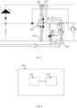
Figure 1 shows an example embodiment of a switch arrangement; -
Figure 2 shows the switch arrangement ofFigure 1 and illustrates operation during a positive ESD strike; -
Figure 3 shows the switch arrangement ofFigure 1 and illustrates operation during a negative ESD strike; -
Figure 4 shows an example battery management system. - The embodiments described relate to a circuit arrangement including a bi-directional MOS based switch and further circuitry to provide electrostatic discharge, ESD, protection. The further circuitry may also improve electromagnetic compatibility and protect the switch against voltage transients caused by hot-plug events.
-
Figure 1 shows aswitch arrangement 100 comprising a metal-oxide-semiconductor, MOS, bi-directional switch 101 (herein referred to as MOS switch) having adrain terminal 102, asource terminal 103, agate terminal 104 and a body orsubstrate terminal 105. Thearrangement 100 is configured as a bi-directional MOS-based switch arrangement. - The
switch arrangement 100 further comprises afirst clamp circuit 107 coupled between thedrain terminal 102, thegate terminal 104 and thesource terminal 103. Thefirst clamp circuit 107 is configured to activate when a voltage greater than a first threshold voltage is applied to thedrain terminal 102, i.e. a VDS voltage of theMOS switch 101 is greater than a first threshold voltage. Thefirst clamp circuit 107, on activation, is configured to raise the voltage at thegate terminal 104 of theswitch 101. The operation of thearrangement 100 and the effect of raising the gate voltage will be described in more detail below. - Returning to the
switch arrangement 100, there is provided afirst transistor 110 having asource terminal 111 coupled to thebody 105 of theMOS switch 101, adrain terminal 112 coupled to thesource terminal 103 of theMOS switch 101 and agate terminal 113 coupled to thegate terminal 104 of theMOS switch 101. Thefirst transistor 110 may comprises an nMOS transistor, such as an nMOS Field Effect Transistor, FET. Thefirst transistor 110 is configured to switch on at the same time as theMOS switch 101. - The
switch arrangement 100 of the present example comprises asecond clamp circuit 115. Thesecond clamp circuit 115, in the present example, comprises afirst diode 116 of Zener diode type having ananode terminal 117 coupled to thebody 105 of theMOS switch 101 and acathode terminal 118 coupled to thesource terminal 103. Thesecond clamp circuit 115 further comprises asecond transistor 119 having asource terminal 120 coupled to thebody 105 of theMOS switch 101, adrain terminal 121 coupled to thesource terminal 103 of theMOS switch 101 and agate terminal 122 coupled to theanode terminal 117 of thefirst diode 116. Thesecond transistor 119 may comprises an nMOS transistor, such as an nMOS FET or an NPN transistor. - In one or more examples, the
second clamp circuit 115 further comprises afirst resistor 123 having a first terminal coupled to thebody 105 of theMOS switch 101 and a second terminal coupled to theanode terminal 117 of the first, Zener,diode 116 such that theanode terminal 117 of the first, Zener,diode 116 is coupled to thebody 105 of theMOS switch 101 via thefirst resistor 123. - In one or more examples, the
first clamp circuit 107 comprises a Zenerdiode 125, termed asecond diode 125, and athird diode 126 which may be a normal p-n diode. Acathode terminal 127 of the Zenerdiode 125 is coupled to thedrain terminal 102 and ananode terminal 128 of the Zenerdiode 125 is coupled to ananode terminal 129 of thethird diode 126. Thecathode terminal 130 of thethird diode 126 is coupled to thegate terminal 104. Thecathode terminal 130 is also coupled to thesource terminal 103 via asecond resistor 131. It will be appreciated that thefirst clamp circuit 107 may take other forms. - The
second resistor 131 is thus electrically coupled between thegate terminal 104 and thesource terminal 103 of theMOS switch 101. - In
figure 1 , thesecond clamp circuit 115 is shown with afourth diode 133 representing a parasitic component of thesecond transistor 119. As will be understood by those skilled in the art, the parasiticfourth diode 133 or "built in body diode", in effect, has a cathode terminal coupled to thedrain terminal 121 of thesecond transistor 119 and an anode terminal coupled to thesource terminal 120 of thesecond transistor 119. Further, in effect, the body of thesecond transistor 119 is connected to itssource terminal 120. - In
figure 1 , thefirst transistor 110 is shown with afifth diode 134 representing a parasitic component of thefirst transistor 110. As will be understood by those skilled in the art, the parasiticfifth diode 134 or "built in body diode", in effect, has a cathode terminal coupled to thedrain terminal 112 of thefirst transistor 110 and an anode terminal coupled to thesource terminal 111 of thefirst transistor 110. Further, in effect, the body of thefirst transistor 110 is connected to itssource terminal 111 by the parasiticfifth diode 134. - Further, in the present example, the
MOS switch 101 also has parasitic components that are shown as built inbody diodes 136, 167. Thus, in effect, thedrain terminal 102 of theMOS switch 101 is coupled to a cathode terminal of a parasiticsixth diode 136, and the source terminal of the MOS switch is coupled to a cathode terminal of a parasiticseventh diode 137 and wherein the anode terminals of the parasiticsixth diode 136 and the parasiticseventh diode 137 are both coupled to thebody 105. - In the event of a positive transient voltage applied to the
drain terminal 102, such as would occur during an electrostatic discharge (ESD) event, thefirst clamp circuit 107 is configured to bias thegate terminal 104 ofMOS switch 101 to make it conducting to allow ESD current due to the positive transient voltage to flow through theMOS switch 101. - Example
figure 2 illustrates the flow of current in the event of such a positive transient voltage. - As mentioned briefly above, the
first clamp circuit 107 is configured to generate a gate to source voltage on the transistor of theMOS switch 101 when the drain to source voltage of the transistor of theMOS switch 101 is higher than a first threshold voltage. - The Zener voltage of the
Zener diode 125 or "second diode" is Vttrig_ZD2. The forward threshold voltage (or "activation voltage") of the third diode is Vd3. In one or more examples, Vd3 may be approximately 0.6V. The threshold voltage of theMOS switch 101 is designated Vt_MOS. Thus, the first threshold voltage or "clamp voltage" is the sum of Vt_MOS + Vttrig_ZD2 + Vd3. Accordingly, when the gate to source voltage of the transistor of theMOS switch 101 is higher than its threshold voltage, the switch will thus conduct the ESD stress current causing the drain to source voltage to be limited to Vt_MOS + Vttrig_ZD2 + Vd3 + Vod. Vod being the overdrive voltage on top of Vt_MOS to get the expected ESD current flowing through theMOS switch 101 with a limited Vds voltage. - Thus, when a transient is applied to the
drain terminal 102 the drain-source voltage, Vds, of theMOS switch 101 may be greater than the first threshold voltage comprising Vt_MOS + Vttrig_ZD2 + Vd3, such that thefirst clamp circuit 107 causes an increase in the gate to source voltage increasing over its threshold voltage, therefore providing the drain to source voltage limitation, as descri bed.
i.e.
- The
first clamp circuit 107 is such that theMOS switch 101 is self-protected because the resultingflow 200 of current through theZener diode 125 and thethird diode 126 acts to raise the voltage at thegate terminal 104 up to the threshold voltage of theMOS switch 101, Vt_MOS. - This allows the current caused by the transient voltage to follow the
path 201 through the channel of theMOS switch 101 to thesource terminal 103. The MOS switch is thereby protected due to the drain to source voltage limitation provided by thefirst clamp circuit 107. - If the roll-off voltage of the
MOS switch 101 is Vrf, then the Zener voltage of theZener diode 125, Vttrig_ZD2, and the forward threshold voltage of the third diode Vd3 may be chosen such that Vttrig_ZD2 + Vd3 + Vt_MOS is lower than Vrf. In one or more examples, a 2 to 3V overdrive voltage is provided between the desired maximum drain source voltage under ESD stress with respect to the breakdown voltage of the transistor of theMOS switch 101. Thus, such a configuration will clamp the drain source voltage VDS around Vttrig_ZD2 + Vd3 + VGS, wherein VGS comprises the gate-source voltage of theMOS switch 101. This is advantageous because the gate source voltage of theMOS switch 101 must be at least the Vt_MOS level to get it conducting current between drain and source. In practice, the gate source voltage gets to few volts higher than Vt_MOS such that drain source on-resistance of the MOS switch x the ESD current is limiting the drain source voltage to the adequate level, such as the breakdown voltage of the MOS switch minus, for example, a margin such as 2.5 V. - In one or more examples, the resistance value of the
second resistor 131 may be selected to makesure MOS switch 101 does not have a floating gate voltage that would cause excessive leakage in its channel. - As mentioned, when the
MOS switch 101 is turned on, thefirst transistor 110 is also configured to turn on substantially simultaneously, thus shorting thebody 105 of theMOS switch 101 to itssource terminal 103. This is advantageous because the transient voltage capability (i.e. the drain-source voltage VDS) of theMOS switch 101 is high, whenbody 105 and thesource terminal 103 are shorted together, preventing the early activation of the parasitic NPN represented by theparasitic diodes switch arrangement 100 may be such that Vbs (the base source voltage) of theMOS switch 101 must be low during ESD stress in order to get the maximum drain-source on resistance performance of transistor of theMOS switch 101 therefore allowing, for example, the lowest possible drain to source voltage when ESD current is flowing through its channel. - In one or more examples, the MOS switch is provided with a low on-resistance, Ron, and may therefore have a large footprint. Accordingly, in one or more examples, the
first transistor 110 has a smaller footprint and is configured to turn on more rapidly than theMOS switch 101, at least during an ESD event. However, in one or more examples, thefirst transistor 110 is configured with an on-resistance low enough to keep the body-source voltage, VBS, of theMOS switch 101 close to 0V due to the fact that its source is also pulled up together with thegate terminal 104 due to thefirst clamp circuit 107. - It will be appreciated that the
first transistor 110 has a smaller size than theMOS switch 101 and therefore the current flow into thefirst transistor 110 is much lower than into theMOS switch 101. - Example
figure 3 illustrates the flow of current in the event of a negative transient voltage. In the present example, it is primarily thesecond clamp circuit 115 that is configured to protect theMOS switch 101 against transient voltage events applied at thesource terminal 103, i.e. a transient voltage applied as a source-drain voltage, VSD, of theMOS switch 101. - The
second clamp circuit 115 may act differently depending on whether the voltage transient at thesource terminal 103 is a fast transient or a relatively slower transient, such as one that may occur during a hot-plug situation. - During a fast transient voltage applied at the
source terminal 103, then the transient may be of a sufficiently high voltage for theMOS switch 101 to be turned on in reverse, that is if the gate-drain voltage is >0. Thus, thefirst diode 116 acts to control the gate source voltage of thesecond transistor 119 to cause thesecond transistor 119 to conduct to receive the ESD current during a fast transient voltage applied at thesource terminal 103, leading to limit the body to source voltage of theMOS switch 101. It may also be noted that the body to drain voltage of theMOS switch 101 may be also limited to around 0.6V due to the built-inbody diode 136 between body and drain, and therefore the Vsd voltage of theMOS switch 101 is also limited in response to negative ESD stress. Acurrent path 300 is also generated due to thegate 104 being connected to thesource 103 via thesecond resistor 131 which results in theMOS switch 101 having a gate drain voltage that makes the channel also conduct negative ESD current. - The
first diode 116, on occurrence of voltage transients at thesource terminal 103 may be configured to provide a gate voltage at the gate of thesecond transistor 119. Thesecond transistor 119 is turned on provided the transient voltage is greater than the Zener voltage of the first, Zener,diode 116 and the threshold voltage of thesecond transistor 119. This is advantageous, because thesecond circuit 115 is configured to, in the event of a transient voltage applied at the source terminal that exceeds the Zener voltage of the first diode 116 (e.g. VSD > Vttrig_ZD1+Vt_2nd_transistor), provide for switching on of thesecond transistor 119 to provide acurrent path 301 from thesource terminal 103, through the channel of thesecond transistor 119, through thebody 105 and to thedrain terminal 102. This may be more likely to occur if theMOS switch 101 is smaller. - During a slower transient voltage applied at the source terminal 103 (which may occur during a hot-plug event), then the
MOS switch 101 may not be susceptible to being turned on in reverse. Then, again, thesecond transistor 119 may be configured to turn on, provided the transient voltage is greater than the Zener voltage of the first, Zener,diode 116 plus its threshold voltage. Thus, thesecond clamp circuit 115 is configured to, in the event of a (slower) transient voltage applied at thesource terminal 103 that exceeds the Zener voltage of thefirst diode 116 and the threshold voltage of thesecond transistor 119, provide for switching on of thesecond transistor 119, due to reversecurrent flow 302 through the first, Zener,diode 116 to the gate of thesecond transistor 119. As before, this provides acurrent path 301 from thesource terminal 103, through the channel of thesecond transistor 119, through thebody 105 and to thedrain terminal 102. - In summary, in the event of a negative transient, i.e. one applied at the source terminal, the
second clamp circuit 115, by virtue of the action of thefirst diode 116 and thesecond transistor 119, is configured to short thebody 105 to thesource terminal 103 which gives the opportunity for self protection of the MOS switch. - It will be appreciated that the triggering of the
second transistor 119 can clamp the source-drain voltage of the MOS switch to a desired value by the Zener voltage of the first, Zener,diode 116. - The
first clamp circuit 107 and thesecond clamp circuit 115 are named as such because at least one of their functions, in some examples, is to clamp a terminal-to-terminal voltage of theMOS switch 101. However, it will be appreciated that thefirst clamp circuit 107 and thesecond clamp circuit 115 may be referred to more generally as afirst circuit 107 and asecond circuit 115. - The
switch arrangement 100 of the present disclosure has particular application in a battery management system. Thus,figure 4 shows abattery management system 400 including theswitch arrangement 100 of preceding embodiments for coupling to abattery 401. In such an implementation,several switch arrangements 100 may be provided together and coupled to thebattery pack 401. - It will be appreciated that any components said to be coupled may be coupled or connected either directly or indirectly. In the case of indirect coupling, additional components may be located between the two components that are said to be coupled.
- In this specification, example embodiments have been presented in terms of a selected set of details. However, a person of ordinary skill in the art would understand that many other example embodiments may be practiced which include a different selected set of these details. It is intended that the following claims cover all possible example embodiments.
Claims (15)
- A switch arrangement comprising:a bi-directional metal-oxide-semiconductor, MOS, switch having a drain terminal, a source terminal, a gate terminal and a body;a first circuit coupled between the drain terminal, the gate terminal and the source terminal for providing electrostatic discharge protection;a first transistor having a source terminal coupled to the body of the MOS switch, a drain terminal coupled to the source terminal of the MOS switch and a gate terminal coupled to the gate terminal of the MOS switch; anda second circuit for providing electrostatic discharge protection comprising a first diode of Zener diode type having an anode terminal coupled to the body of the MOS switch and a cathode terminal coupled to the source terminal, and a second transistor having a source terminal coupled to the body of the MOS switch, a drain terminal coupled to the source terminal of the MOS switch and a gate terminal coupled to the anode terminal of the first diode.
- The switch arrangement of claim 1, wherein the second circuit further comprises a first resistor having a first terminal coupled to the body of the MOS switch and a second terminal coupled to the anode terminal of the first diode such that the anode terminal of the first diode is coupled to the body of the MOS switch via the first resistor in series.
- The switch arrangement of claim 1 or claim 2, wherein the first circuit comprises:a second diode of Zener diode type and a third diode,wherein a cathode terminal of the second diode is coupled to the drain terminal and an anode terminal of the second diode is coupled to an anode terminal of the third diode, and the cathode terminal of the third diode is coupled to the gate terminal.
- The switch arrangement of claim 3, wherein the first circuit further comprises a second resistor connected between the gate terminal and the source terminal.
- The switch arrangement of any preceding claim, wherein the first transistor comprises an nMOS MOSFET.
- The switch arrangement of any preceding claim, wherein the second transistor comprises an nMOS FET.
- The switch arrangement of any preceding claim, wherein the second transistor comprises an NPN transistor.
- The switch arrangement of any preceding claim, wherein the MOS switch is provided with an on-resistance lower than the on-resistance of the first transistor.
- The switch arrangement of any preceding claim, wherein MOS switch is an n-channel MOS switch.
- The switch arrangement of claim 3 or 4, wherein a forward threshold voltage of the third diode plus a Zener voltage of the second diode plus a threshold voltage of the MOS switch plus an overdrive voltage of the MOS switch is selected to be less than a roll-off voltage of the MOS switch.
- The switch arrangement of any preceding claim, wherein the first transistor is configured to turn on when the MOS switch turns on to short the body of the MOS switch to its source terminal.
- The switch arrangement of any preceding claim, wherein the second transistor is configured to short the body of the MOS switch to the source terminal upon the occurrence of a transient voltage applied to the source terminal that exceeds the Zener voltage of the first diode plus a threshold voltage of the second transistor.
- The switch arrangement of any preceding claim, wherein the Zener voltage of the first diode is selected such that based on the occurrence of an electrostatic discharge event applied to the source terminal of the MOS switch which is of a voltage greater than said Zener voltage plus a threshold voltage of the second transistor, the second transistor is switched on to open a current path from the source terminal of the MOS switch, through the second transistor, the body and to the drain terminal of the MOS switch.
- The switch arrangement of any preceding claim, wherein the switch arrangement comprises a bi-directional MOS-based switch arrangement.
- A battery management system including the switch arrangement of any preceding claim.
Priority Applications (3)
| Application Number | Priority Date | Filing Date | Title |
|---|---|---|---|
| EP23306650.5A EP4531105B1 (en) | 2023-09-29 | 2023-09-29 | An electrostatic discharge protectionusing a mos-based switch |
| CN202411106782.7A CN119743130A (en) | 2023-09-29 | 2024-08-13 | switch |
| US18/886,224 US12633910B2 (en) | 2023-09-29 | 2024-09-16 | Switch |
Applications Claiming Priority (1)
| Application Number | Priority Date | Filing Date | Title |
|---|---|---|---|
| EP23306650.5A EP4531105B1 (en) | 2023-09-29 | 2023-09-29 | An electrostatic discharge protectionusing a mos-based switch |
Publications (2)
| Publication Number | Publication Date |
|---|---|
| EP4531105A1 true EP4531105A1 (en) | 2025-04-02 |
| EP4531105B1 EP4531105B1 (en) | 2026-04-29 |
Family
ID=88296989
Family Applications (1)
| Application Number | Title | Priority Date | Filing Date |
|---|---|---|---|
| EP23306650.5A Active EP4531105B1 (en) | 2023-09-29 | 2023-09-29 | An electrostatic discharge protectionusing a mos-based switch |
Country Status (2)
| Country | Link |
|---|---|
| EP (1) | EP4531105B1 (en) |
| CN (1) | CN119743130A (en) |
Citations (3)
| Publication number | Priority date | Publication date | Assignee | Title |
|---|---|---|---|---|
| US20120161232A1 (en) * | 2010-12-28 | 2012-06-28 | Texas Instruments Incorporated | Robust esd cell with adjustable holding voltage for advanced analog technologies |
| US9263428B2 (en) * | 2006-08-24 | 2016-02-16 | Infineon Technologies Ag | Diode biased ESD protection device and method |
| US20230268338A1 (en) * | 2022-01-17 | 2023-08-24 | Stmicroelectronics Sa | Electrostatic discharge protection device |
-
2023
- 2023-09-29 EP EP23306650.5A patent/EP4531105B1/en active Active
-
2024
- 2024-08-13 CN CN202411106782.7A patent/CN119743130A/en active Pending
Patent Citations (3)
| Publication number | Priority date | Publication date | Assignee | Title |
|---|---|---|---|---|
| US9263428B2 (en) * | 2006-08-24 | 2016-02-16 | Infineon Technologies Ag | Diode biased ESD protection device and method |
| US20120161232A1 (en) * | 2010-12-28 | 2012-06-28 | Texas Instruments Incorporated | Robust esd cell with adjustable holding voltage for advanced analog technologies |
| US20230268338A1 (en) * | 2022-01-17 | 2023-08-24 | Stmicroelectronics Sa | Electrostatic discharge protection device |
Also Published As
| Publication number | Publication date |
|---|---|
| CN119743130A (en) | 2025-04-01 |
| EP4531105B1 (en) | 2026-04-29 |
| US20250112630A1 (en) | 2025-04-03 |
Similar Documents
| Publication | Publication Date | Title |
|---|---|---|
| CN108123596B (en) | NMOS switching tube driving circuit | |
| US7427887B2 (en) | Open drain driver, and a switch comprising the open drain driver | |
| US9088158B2 (en) | Reverse voltage condition protection in a power supply system | |
| EP2071724B1 (en) | Power supply control circuit | |
| US8299841B2 (en) | Semiconductor device | |
| US7280328B2 (en) | Semiconductor integrated circuit device | |
| EP1063757A2 (en) | Power MOSFET having voltage-clamped gate | |
| US6078487A (en) | Electro-static discharge protection device having a modulated control input terminal | |
| CN110838836B (en) | Fault Tolerant Low Leakage Switch | |
| JPH08275406A (en) | Battery disconnect switch and battery disconnect switch system | |
| US8233252B2 (en) | ESD protection circuit for low voltages | |
| US20130099297A1 (en) | Electrostatic discharge protection device | |
| US20210376596A1 (en) | Inrush current limiter and system including the same | |
| CN107968567B (en) | NMOS switching tube driving circuit | |
| US7855863B2 (en) | Driver with electrostatic discharge protection | |
| CN110855277B (en) | Adjustable clamping circuit | |
| US6633470B2 (en) | Overvoltage protection circuit for bidirectional transmission gate | |
| EP4531105B1 (en) | An electrostatic discharge protectionusing a mos-based switch | |
| US12633910B2 (en) | Switch | |
| US10396068B2 (en) | Electrostatic discharge protection device | |
| KR20200077746A (en) | Electrostatic discharge protection circuit | |
| US20180102642A1 (en) | Electrostatic discharge circuit | |
| US11811221B2 (en) | Electrostatic discharge protection device | |
| JP2003264233A (en) | Semiconductor integrated circuit device | |
| US9741705B1 (en) | Compact ESD bootstrap clamp |
Legal Events
| Date | Code | Title | Description |
|---|---|---|---|
| PUAI | Public reference made under article 153(3) epc to a published international application that has entered the european phase |
Free format text: ORIGINAL CODE: 0009012 |
|
| STAA | Information on the status of an ep patent application or granted ep patent |
Free format text: STATUS: THE APPLICATION HAS BEEN PUBLISHED |
|
| AK | Designated contracting states |
Kind code of ref document: A1 Designated state(s): AL AT BE BG CH CY CZ DE DK EE ES FI FR GB GR HR HU IE IS IT LI LT LU LV MC ME MK MT NL NO PL PT RO RS SE SI SK SM TR |
|
| STAA | Information on the status of an ep patent application or granted ep patent |
Free format text: STATUS: REQUEST FOR EXAMINATION WAS MADE |
|
| 17P | Request for examination filed |
Effective date: 20251002 |
|
| REG | Reference to a national code |
Ref country code: DE Ref legal event code: R079 Free format text: PREVIOUS MAIN CLASS: H01L0027020000 Ipc: H10D0089600000 Ref document number: 602023016123 Country of ref document: DE |
|
| GRAP | Despatch of communication of intention to grant a patent |
Free format text: ORIGINAL CODE: EPIDOSNIGR1 |
|
| STAA | Information on the status of an ep patent application or granted ep patent |
Free format text: STATUS: GRANT OF PATENT IS INTENDED |
|
| RIC1 | Information provided on ipc code assigned before grant |
Ipc: H10D 89/60 20250101AFI20260127BHEP Ipc: H10D 89/00 20250101ALI20260127BHEP |
|
| INTG | Intention to grant announced |
Effective date: 20260205 |
|
| GRAS | Grant fee paid |
Free format text: ORIGINAL CODE: EPIDOSNIGR3 |
|
| GRAA | (expected) grant |
Free format text: ORIGINAL CODE: 0009210 |
|
| STAA | Information on the status of an ep patent application or granted ep patent |
Free format text: STATUS: THE PATENT HAS BEEN GRANTED |
|
| AK | Designated contracting states |
Kind code of ref document: B1 Designated state(s): AL AT BE BG CH CY CZ DE DK EE ES FI FR GB GR HR HU IE IS IT LI LT LU LV MC ME MK MT NL NO PL PT RO RS SE SI SK SM TR |
|
| REG | Reference to a national code |
Ref country code: CH Ref legal event code: F10 Free format text: ST27 STATUS EVENT CODE: U-0-0-F10-F00 (AS PROVIDED BY THE NATIONAL OFFICE) Effective date: 20260429 Ref country code: GB Ref legal event code: FG4D |