EP4531045A1 - Decoder, decoding method, memory controller and memory system - Google Patents
Decoder, decoding method, memory controller and memory system Download PDFInfo
- Publication number
- EP4531045A1 EP4531045A1 EP23925600.1A EP23925600A EP4531045A1 EP 4531045 A1 EP4531045 A1 EP 4531045A1 EP 23925600 A EP23925600 A EP 23925600A EP 4531045 A1 EP4531045 A1 EP 4531045A1
- Authority
- EP
- European Patent Office
- Prior art keywords
- codeword
- coded
- vector
- hard
- module
- Prior art date
- Legal status (The legal status is an assumption and is not a legal conclusion. Google has not performed a legal analysis and makes no representation as to the accuracy of the status listed.)
- Pending
Links
Images








Classifications
-
- G—PHYSICS
- G11—INFORMATION STORAGE
- G11C—STATIC STORES
- G11C16/00—Erasable programmable read-only memories
- G11C16/02—Erasable programmable read-only memories electrically programmable
- G11C16/06—Auxiliary circuits, e.g. for writing into memory
- G11C16/08—Address circuits; Decoders; Word-line control circuits
-
- G—PHYSICS
- G06—COMPUTING OR CALCULATING; COUNTING
- G06F—ELECTRIC DIGITAL DATA PROCESSING
- G06F11/00—Error detection; Error correction; Monitoring
- G06F11/07—Responding to the occurrence of a fault, e.g. fault tolerance
- G06F11/08—Error detection or correction by redundancy in data representation, e.g. by using checking codes
- G06F11/10—Adding special bits or symbols to the coded information, e.g. parity check, casting out 9's or 11's
- G06F11/1008—Adding special bits or symbols to the coded information, e.g. parity check, casting out 9's or 11's in individual solid state devices
- G06F11/1012—Adding special bits or symbols to the coded information, e.g. parity check, casting out 9's or 11's in individual solid state devices using codes or arrangements adapted for a specific type of error
-
- G—PHYSICS
- G06—COMPUTING OR CALCULATING; COUNTING
- G06F—ELECTRIC DIGITAL DATA PROCESSING
- G06F7/00—Methods or arrangements for processing data by operating upon the order or content of the data handled
- G06F7/76—Arrangements for rearranging, permuting or selecting data according to predetermined rules, independently of the content of the data
- G06F7/78—Arrangements for rearranging, permuting or selecting data according to predetermined rules, independently of the content of the data for changing the order of data flow, e.g. matrix transposition or LIFO buffers; Overflow or underflow handling therefor
-
- G—PHYSICS
- G11—INFORMATION STORAGE
- G11C—STATIC STORES
- G11C8/00—Arrangements for selecting an address in a digital store
- G11C8/10—Decoders
-
- H—ELECTRICITY
- H03—ELECTRONIC CIRCUITRY
- H03M—CODING; DECODING; CODE CONVERSION IN GENERAL
- H03M13/00—Coding, decoding or code conversion, for error detection or error correction; Coding theory basic assumptions; Coding bounds; Error probability evaluation methods; Channel models; Simulation or testing of codes
- H03M13/03—Error detection or forward error correction by redundancy in data representation, i.e. code words containing more digits than the source words
- H03M13/05—Error detection or forward error correction by redundancy in data representation, i.e. code words containing more digits than the source words using block codes, i.e. a predetermined number of check bits joined to a predetermined number of information bits
- H03M13/09—Error detection only, e.g. using cyclic redundancy check [CRC] codes or single parity bit
- H03M13/095—Error detection codes other than CRC and single parity bit codes
- H03M13/096—Checksums
-
- H—ELECTRICITY
- H03—ELECTRONIC CIRCUITRY
- H03M—CODING; DECODING; CODE CONVERSION IN GENERAL
- H03M13/00—Coding, decoding or code conversion, for error detection or error correction; Coding theory basic assumptions; Coding bounds; Error probability evaluation methods; Channel models; Simulation or testing of codes
- H03M13/03—Error detection or forward error correction by redundancy in data representation, i.e. code words containing more digits than the source words
- H03M13/05—Error detection or forward error correction by redundancy in data representation, i.e. code words containing more digits than the source words using block codes, i.e. a predetermined number of check bits joined to a predetermined number of information bits
- H03M13/11—Error detection or forward error correction by redundancy in data representation, i.e. code words containing more digits than the source words using block codes, i.e. a predetermined number of check bits joined to a predetermined number of information bits using multiple parity bits
- H03M13/1102—Codes on graphs and decoding on graphs, e.g. low-density parity check [LDPC] codes
- H03M13/1105—Decoding
- H03M13/1108—Hard decision decoding, e.g. bit flipping, modified or weighted bit flipping
-
- H—ELECTRICITY
- H03—ELECTRONIC CIRCUITRY
- H03M—CODING; DECODING; CODE CONVERSION IN GENERAL
- H03M13/00—Coding, decoding or code conversion, for error detection or error correction; Coding theory basic assumptions; Coding bounds; Error probability evaluation methods; Channel models; Simulation or testing of codes
- H03M13/03—Error detection or forward error correction by redundancy in data representation, i.e. code words containing more digits than the source words
- H03M13/05—Error detection or forward error correction by redundancy in data representation, i.e. code words containing more digits than the source words using block codes, i.e. a predetermined number of check bits joined to a predetermined number of information bits
- H03M13/11—Error detection or forward error correction by redundancy in data representation, i.e. code words containing more digits than the source words using block codes, i.e. a predetermined number of check bits joined to a predetermined number of information bits using multiple parity bits
- H03M13/1102—Codes on graphs and decoding on graphs, e.g. low-density parity check [LDPC] codes
- H03M13/1148—Structural properties of the code parity-check or generator matrix
- H03M13/116—Quasi-cyclic LDPC [QC-LDPC] codes, i.e. the parity-check matrix being composed of permutation or circulant sub-matrices
-
- H—ELECTRICITY
- H03—ELECTRONIC CIRCUITRY
- H03M—CODING; DECODING; CODE CONVERSION IN GENERAL
- H03M13/00—Coding, decoding or code conversion, for error detection or error correction; Coding theory basic assumptions; Coding bounds; Error probability evaluation methods; Channel models; Simulation or testing of codes
- H03M13/37—Decoding methods or techniques, not specific to the particular type of coding provided for in groups H03M13/03 - H03M13/35
- H03M13/3707—Adaptive decoding and hybrid decoding, e.g. decoding methods or techniques providing more than one decoding algorithm for one code
- H03M13/3715—Adaptation to the number of estimated errors or to the channel state
-
- H—ELECTRICITY
- H03—ELECTRONIC CIRCUITRY
- H03M—CODING; DECODING; CODE CONVERSION IN GENERAL
- H03M13/00—Coding, decoding or code conversion, for error detection or error correction; Coding theory basic assumptions; Coding bounds; Error probability evaluation methods; Channel models; Simulation or testing of codes
- H03M13/37—Decoding methods or techniques, not specific to the particular type of coding provided for in groups H03M13/03 - H03M13/35
- H03M13/3723—Decoding methods or techniques, not specific to the particular type of coding provided for in groups H03M13/03 - H03M13/35 using means or methods for the initialisation of the decoder
-
- H—ELECTRICITY
- H03—ELECTRONIC CIRCUITRY
- H03M—CODING; DECODING; CODE CONVERSION IN GENERAL
- H03M13/00—Coding, decoding or code conversion, for error detection or error correction; Coding theory basic assumptions; Coding bounds; Error probability evaluation methods; Channel models; Simulation or testing of codes
- H03M13/37—Decoding methods or techniques, not specific to the particular type of coding provided for in groups H03M13/03 - H03M13/35
- H03M13/3738—Decoding methods or techniques, not specific to the particular type of coding provided for in groups H03M13/03 - H03M13/35 with judging correct decoding
-
- H—ELECTRICITY
- H03—ELECTRONIC CIRCUITRY
- H03M—CODING; DECODING; CODE CONVERSION IN GENERAL
- H03M13/00—Coding, decoding or code conversion, for error detection or error correction; Coding theory basic assumptions; Coding bounds; Error probability evaluation methods; Channel models; Simulation or testing of codes
- H03M13/37—Decoding methods or techniques, not specific to the particular type of coding provided for in groups H03M13/03 - H03M13/35
- H03M13/45—Soft decoding, i.e. using symbol reliability information
- H03M13/458—Soft decoding, i.e. using symbol reliability information by updating bit probabilities or hard decisions in an iterative fashion for convergence to a final decoding result
-
- H—ELECTRICITY
- H03—ELECTRONIC CIRCUITRY
- H03M—CODING; DECODING; CODE CONVERSION IN GENERAL
- H03M13/00—Coding, decoding or code conversion, for error detection or error correction; Coding theory basic assumptions; Coding bounds; Error probability evaluation methods; Channel models; Simulation or testing of codes
- H03M13/27—Coding, decoding or code conversion, for error detection or error correction; Coding theory basic assumptions; Coding bounds; Error probability evaluation methods; Channel models; Simulation or testing of codes using interleaving techniques
-
- H—ELECTRICITY
- H03—ELECTRONIC CIRCUITRY
- H03M—CODING; DECODING; CODE CONVERSION IN GENERAL
- H03M13/00—Coding, decoding or code conversion, for error detection or error correction; Coding theory basic assumptions; Coding bounds; Error probability evaluation methods; Channel models; Simulation or testing of codes
- H03M13/61—Aspects and characteristics of methods and arrangements for error correction or error detection, not provided for otherwise
- H03M13/615—Use of computational or mathematical techniques
- H03M13/616—Matrix operations, especially for generator matrices or check matrices, e.g. column or row permutations
Definitions
- the present disclosure relates to the field of memory technologies, and in particular to a coder, a coding method, a memory controller and a memory system.
- 3D NAND flash memory Flash has evolved from Singe Level Cells (SLC) that can store 1 bit of information and Double Level Cells (DLC) that can store 2 bits of information to Triple Level Cells (TLC) that can store 3 bits of information, and even Quadruple Level Cells (QLC) that can store 4 bits of information.
- SLC Singe Level Cells
- DLC Double Level Cells
- TLC Triple Level Cells
- QLC Quadruple Level Cells
- LDPC low density parity check
- 3D NAND Flash the complex structure of 3D NAND Flash and more data it stores, the types of errors it contains become more and more complex.
- the current error correction methods suffer from the low error correction speed and the inefficiency, which seriously affects the reading rate.
- the examples of the present disclosure provide a coder, a coding method, a memory controller and a memory system.
- an example of the present disclosure provides a coder comprising: a cache module and a flip indication module, wherein;
- the flip indication module is further configured to:
- the coder further comprises a variable node module and a check node module that are connected to form a variable-check connection network according to a pre-constructed check matrix;
- the flip indication module is further configured to:
- the flip indication module is further configured to:
- the flip indication module is further configured to:
- the flipping criterion comprises:
- the coder further comprises: a counting module and a termination decision module, wherein,
- the coder further comprises a rearrangement module
- the termination decision module is further configured to: when the checksum vector is not a zero vector and the number of iterations has not reached the maximum number of iterations, output a continue coding signal, and the continue coding signal is configured to: instruct the variable node module, the check node module and the flip indication module to continue to perform a hard-decision coding operation on the codeword to be coded.
- an example of the present disclosure provides a coding method, comprising:
- the determining, with assistance of the soft data, the number of parity checks not satisfied by the bits in the codeword to be coded comprises:
- the determining, with assistance of the soft data in combination with the initial error bit indication vector, the number of parity checks not satisfied by the bits in the codeword to be coded comprises:
- the determining the initial error bit indication vector corresponding to the codeword to be coded comprises:
- the determining the initial error bit indication vector corresponding to the codeword to be coded according to the hard-read data, the codeword to be coded, the checksum vector, and the check matrix comprises:
- the method further comprises:
- the method further comprises:
- the flipping criterion comprises:
- the method further comprises:
- the method further comprises:
- the method further comprises: when the checksum vector is not a zero vector and the number of iterations has not reached the maximum number of iterations, output a continue coding signal, wherein the continue coding signal is configured to instruct to perform a hard-decision coding operation on the codeword to be coded.
- an example of the present disclosure provides a memory system, comprising:
- the processor is further configured to: read hard-read data from the memory device; and send the hard-read data to the coder; and the coder is further configured to: receive the hard-read data and generate the codeword to be coded according to the hard-read data.
- the coder comprises: a cache module, a variable node module, a check node module, and a flip indication module, wherein,
- the coder provided by the example of the present disclosure caches the soft data related to the codeword to be coded through the included buffer module, and then the flip indication module, when performing hard-decision coding on the codeword to be coded, determines, with assistance of the soft data, a number of parity checks not satisfied by bits in the codeword to be coded in one or more iterations.
- the soft data is used to assist the flipping decision of the hard-decision coding to enable high throughput and low power consumption of the hard-decision coding, greatly improving the error correction capability of hard-decision coding.
- first element in one example may also be referred to as a second or third element in another example without departing from the spirit and scope of the examples of the present disclosure.
- a memory device is memory equipment used to preserve information in modern information technology.
- 3D NAND (Not-And) type memory device has become a mainstream product in the storage market due to its high storage density, controllable production cost, suitable programming and erasing speed and retention characteristics.
- the types of errors that occur during the read operation of the memory device become more and more complex.
- LDPC hard-decision coding in the coder is used to code the codeword to be coded (data read from the memory device)
- the coding time is longer and the error correction capability is weaker, which seriously affects the reading rate.
- an example of the present disclosure provides a coder that utilizes soft data to assist the flip decision of hard-decision coding, and realizes the characteristics of high throughput and low power consumption of hard-decision coding, thus greatly improving he error correction capability of hard-decision coding.
- FIG. 1 is a schematic diagram of an example system having a memory system according to an example of the present disclosure.
- the system 100 can be a mobile phone, a desktop computer, a laptop computer, a tablet, a vehicle computer, a gaming console, a printer, a positioning device, a wearable electronic device, a smart sensor, a virtual reality (VR) device, an argument reality (AR) device, or any other suitable electronic devices having a memory system therein.
- system 100 can include a host 108 and a memory system 102.
- the host 108 may include a processor, such as a Central Processing Unit (CPU) or a System of Chip (SoC).
- SoC System of Chip
- the SoC may be, for example, an Application Processor (AP).
- AP Application Processor
- the host 108 further includes at least one operating system (OS) that can generally manage and control the functions and operations performed in the host 108.
- the OS may enable interoperability between a host 108 coupled to the memory system 102 and users who need and use the memory system 102.
- the OS may support functions and operations corresponding to user's requests.
- the OS may be classified into a general-purpose operating system and a mobile operating system.
- the general-purpose operating system can include personal operating systems, which may be an operating system that is used to support services for general purpose including Windows and Chrome, and enterprise operating systems, which may be an operating system specially designed to ensure and support high performance including Windows Server, Linux, Unix, etc.
- the mobile operating system may refer to an operating system for mobility services or functions (e.g., power saving function). Generally speaking, the mobile operating system may be an operating system such as Android, iOS, and Windows Mobile.
- the host 108 may include multiple Oss.
- the host 108 may run multiple operating systems related to the memory system 102.
- the host 108 converts the user's request into one or more commands, and transmits the one or more commands to the memory system 102, so that the memory system 102 executes operations related to the one or more commands.
- the memory system 102 is capable of operating or performing specific functions or performing various internal operations in response to a request from the host 108. In some examples, the memory system 102 is capable of storing data accessed by the host 108.
- the memory system 102 can function as a primary memory system or a secondary memory system for the host 108.
- the memory system 102 and the host 108 can be electrically coupled and communicate according to corresponding protocols.
- the memory system 102 can be implemented and packaged into different types of end electronic products, including, but not limited to: Solid State Drive (SSD), Multimedia Card (MMC), Embedded MMC (eMMC), Reduced Size MMC (RSMMC), Micro MMC, Secure Digital (SD) cards, Mini SD, Micro SD, Universal Serial Bus (USB) storage devices, Universal Flash Memory (UFS) devices, Compact Flash (CF) cards, Smart Media (SM) cards and memory sticks, and so on.
- SSD Solid State Drive
- MMC Multimedia Card
- eMMC Embedded MMC
- RMSMC Reduced Size MMC
- Micro MMC Secure Digital (SD) cards, Mini SD, Micro SD, Universal Serial Bus (USB) storage devices, Universal Flash Memory (UFS) devices, Compact Flash (CF) cards, Smart Media (SM) cards and memory sticks, and so on.
- SSD Solid State Drive
- MMC Multimedia Card
- eMMC Embedded MMC
- RSMMC Reduced Size MMC
- Micro MMC Secure Digital (SD
- the memory system 102 may also be configured as part of, for example, computers, ultra-mobile PCs (UMPCs), workstations, netbooks, personal digital assistants (PDAs), portable computers, web tablets, tablet computers, wireless phones, mobile phones, smart phones, e-books, portable multimedia players (PMPs), portable game consoles, navigation systems, black boxes, digital cameras, digital multimedia broadcasting (DMB) players, three-dimensional (3D) televisions, smart TVs, digital audio recorders, digital audio players, digital picture recorders, digital picture players, digital video recorders, digital video players, storage devices configured with a data center, devices capable of transmitting and receiving information in a wireless environment, one of various electronic devices configured with a home network, one of various electronic devices configured with a computer network, one of various electronic devices configured with telematics network, radio frequency identification (RFID) devices, or one of the various components configured with a computing system.
- UMPCs ultra-mobile PCs
- PDAs personal digital assistants
- portable computers web tablets, tablet computers, wireless phones,
- the memory system 102 may include one or more memory devices 104 and a memory controller 106.
- the memory controller 106 can respond to the request of the host 108, and then control the memory device 104.
- the memory controller 106 can read data from the memory device 104, and transmit the read data to the host 108.
- the memory controller 106 can receive data to be stored from the host 108, and store the data to be stored into the memory device 104. That is, the memory controller 106 is capable of controlling write (or program) operations, read operations, erase operations, background operations, and the like of the memory device 104.
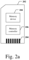
- the memory system 102 can be implemented and packaged into different types of end electronic products. In one example as shown in FIG.
- Memory card 202 can include a PC card (PCMCIA, personal computer memory card international association), a CF card, a smart media (SM) card, a memory stick, a multimedia card (MMC, RS-MMC, MMCmicro), an SD card (SD, miniSD, microSD, SDHC), a UFS, etc.
- Memory card 202 can further include a memory card connector 204 coupling memory card 202 with a host (e.g., host 108 in FIG. 1 ).
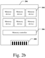
- memory controller 206 and multiple memory devices 104 may be integrated into an SSD 206.
- SSD 206 can further include an SSD connector 208 coupling SSD 206 with a host (e.g., host 108 in FIG. 1 ). In some examples, at least one of the storage capacity or the operation speed of SSD 206 is greater than those of memory card 202.
- the memory controller 106 may include a host I/F (or front-end interface) 301, a memory I/F (or back-end interface) 302, a processor 303, and a memory 304.
- the above-mentioned components 301, 302, 303, and 304 of the memory controller 106 in the memory controller 106 can share transmission signals inside the memory controller 106 through an internal bus.
- the host I/F 301 can interface the host 108 with the memory system 102 in response to the protocol of host 108, and the host I/F 301 exchanges transfer commands and data operations between the host 108 and the memory system 102.
- the host I/F 301 can process commands and data sent by the host 108, and can include at least one of the followings: Universal Serial Bus (USB), Multimedia Card (MMC), Peripheral Component Interconnect Express (PCI-e or PCIe), Small Computer System Interface (SCSI), Serial SCSI (SAS), Serial Advanced Technology Attachment (SATA), Parallel Advanced Technology Attachment (PATA), Small Computer System Interface (SCSI), Enhanced Small Disk Interface (ESDI), and Electronics Integration drive (IDE).
- USB Universal Serial Bus
- MMC Multimedia Card
- PCI-e or PCIe Peripheral Component Interconnect Express
- SCSI Small Computer System Interface
- SAS Serial SCSI
- SAS Serial Advanced Technology Attachment
- PATA Parallel Advanced Technology Attachment
- SCSI Small Computer System Interface
- ESDI Enhanced Small Disk Interface
- IDE Electronics Integration drive
- the host I/F 301 is a component of the memory system 102 used to exchange data with the host 108 and may be implemented by firmware called a host interface layer
- the memory I/F 302 may be an interface for commands and data transferred between memory controller 106 and memory device 104, allowing memory controller 106 to control the memory device 104 in response to requests communicated from the host 108.
- the memory I/F 302 may generate control signals for controlling the memory device 104.
- the memory I/F 302 can write data into the memory device 104 or read data from the memory device 104 under the control of the processor 303.
- the memory I/F 302 can handle commands and data between the memory controller 106 and the memory device 104, for example, the operation of the NAND flash interface, especially the operation between the memory controller 106 and the memory device 104.
- the memory I/F 302 may be implemented as a component for exchanging data with the memory device 104 by firmware called a Flash Interface Layer (FIL).
- FIL Flash Interface Layer
- the processor 303 may be implemented by a microprocessor or a central processing unit (CPU).
- the memory system 102 may include one or more processors 303.
- the processor 303 can control the overall operation of the memory system 102.
- the processor 303 may control a program operation or a read operation of the memory device 104 in response to a write request or a read request from the host 108.
- the processor 303 may use or run firmware to control the overall operation of the memory system 102.
- firmware may be referred to as a flash translation layer (FTL).
- the FTL may operate as an interface between the host 108 and the memory device 104.
- the host 108 can transmit requests related to write operations and read operations to the memory device 104 through the FTL.
- the memory controller 106 uses the processor 303 when performing an operation requested from the host 108 in the memory device 104.
- the processor 303 coupled to memory device 104 may process instructions or commands related to commands from the host 108.
- the memory controller 106 can perform a foreground operation such as a command operation corresponding to a command input from the host 108, for example, a program operation corresponding to a write command, a read operation corresponding to a read command, and an erase/discard operation corresponding to an erase/discard command, and a parameter setting operation corresponding to a set parameter command or a set feature command with a set command.
- the memory controller 106 may perform background operations on the memory device 104 by the processor 303.
- the background operations may include garbage collection (GC) operations, wear leveling (WL) operations, map clear operations, and bad block management operations that check or search for bad blocks.
- the garbage collection operations may include operations to copy and process data stored in a certain memory block in the memory device 104 to another memory block.
- the wear leveling operations may include operations to swap and process stored data between memory blocks of the memory device 104.
- the map clear operations may include operations to store map data stored in the memory controller 106 into memory blocks of the memory device 104.
- the bad block management operations may include operations to check and process bad blocks in memory blocks of the memory device 104.
- the memory controller 106 may respond to operations to access memory blocks of the memory device 104.
- the operations to access the memory blocks of the memory device 104 may include foreground or background operations performed on the memory blocks of the memory device 104.
- the memory 304 may be a working memory of the memory controller 106 and is configured to store data used to drive the memory controller 106. More specifically, when the memory controller 106 controls the memory device 104 in response to a request from the host 108, the memory 304 can store firmware driven by the processor 303 and data (e.g., metadata) required to drive the firmware.
- the memory 304 may also be a buffer memory of the memory controller 106 and is configured to temporarily store the write data transferred from the host 108 to the memory device 104 and the read data transferred from the memory device 104 to the host 108.
- the memory 304 may include program memory, data memory, write buffer/cache, read buffer/cache, data buffer/cache, and map buffer/cache for storing the write data and the read data.
- the memory 304 may be implemented using volatile memory.
- the memory 304 may be implemented using static random access memory (SRAM), dynamic random access memory (DRAM), or both.
- FIG. 3 shows the memory 304 being included in the memory controller 106, the present disclosure is limited thereto.
- the memory 304 may be external to the memory controller 106, and the memory controller 106 may input and output data to and from memory 304 via a separate memory interface (not shown).
- An error correction (ECC) module 305 is provided with an encoding section 3051 and a decoding section 3052.
- the encoding section 3051 can perform an encoding operation such as LDPC on data to be programmed into the semiconductor memory device 104, and output data including an additional parity check bit.
- the parity check bit may be stored in the semiconductor memory device 104.
- the decoding section 3052 can perform error correction decoding on the data read from the semiconductor memory device 104, determine whether the error correction decoding is successful, output an instruction signal based on the determination result, and use the parity check bit generated by the LDPC encoding operation to correct error bits of data.
- FIG. 3 shows that the error correction module 305 is included in the memory controller 106, the present disclosure is not limited thereto.
- the error correction module 305 may be external to the memory controller 106, and the memory controller 106 may be in data communication with the error correction module 305 via a separate interface (not shown).
- the memory device 104 may include non-volatile memory that retains data stored therein even when power is not supplied.
- the memory device 104 may further include volatile storage memory.
- the device 104 can store data provided from the host 108 through a write operation.
- the memory device 104 can also provide the stored data to the host 108 through a read operation.
- the memory device 104 may include any memory disclosed, for example, volatile memory devices such as dynamic random access memory (DRAM) and static RAM (SRAM), or non-volatile memory devices such as Read-Only Memory (ROM), Mask ROM (MROM), Programmable ROM (PROM), Erasable Programmable ROM (EPROM), Electrically Erasable Programmable ROM (EEPROM), Ferroelectric RAM (FRAM), Phase Change RAM (PRAM), Magnetic Resistive RAM (MRAM), Resistive RAM (RRAM or ReRAM), and flash memory (such as three-dimensional NAND flash memory).
- volatile memory devices such as dynamic random access memory (DRAM) and static RAM (SRAM)
- non-volatile memory devices such as Read-Only Memory (ROM), Mask ROM (MROM), Programmable ROM (PROM), Erasable Programmable ROM (EPROM), Electrically Erasable Programmable ROM (EEPROM), Ferroelectric RAM (FRAM), Phase Change RAM (PRAM), Magnetic Resistive RAM (MRAM), Resistive RAM (R
- the memory device is illustrated by taking a three-dimensional NAND flash memory as an example.
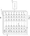
- FIG. 4 it shows a schematic circuit diagram of an example memory device 400 including peripheral circuits according to some aspects of the present disclosure.
- the memory device 400 may be an example of the memory device 104 in FIG. 1 .
- the memory device 400 may include a memory array 401 and a peripheral circuit 402 coupled to the memory array 401.
- the memory array 401 is illustrated by taking a three-dimensional NAND type memory array as an example.
- the memory cells 406 are provided in the form of an array of NAND memory strings 408 each extending vertically above a substrate (not shown).
- each NAND memory string 408 includes a plurality of memory cells 406 coupled in series and stacked vertically.
- Each memory cell 406 can hold a continuous, analog value, such as an electrical voltage or charge, that depends on the number of electrons trapped within a region of memory cell 406.
- Each memory cell 406 can be either a floating gate type of memory cell including a floating-gate transistor or a charge trap type of memory cell including a charge trap transistor.
- each memory cell 406 is a single-level cell (SLC) that has two possible memory states and thus, can store one bit of data.
- the first memory state "0" can correspond to a first range of voltages
- the second memory state "1" can correspond to a second range of voltages.
- each memory cell 406 is a multi-level cell (MLC) that is capable of storing more than a single bit of data in more than four memory states.
- the MLC can store two bits per cell, three bits per cell (also known as trinary-level cell (TLC)), four bits per cell (also known as a quad-level cell (QLC)), or five bits per cell (also known as a penta-level cell (PLC)).
- TLC trinary-level cell
- QLC quad-level cell
- PLC penta-level cell
- Each MLC can be programmed to assume a range of possible nominal storage values. In one example, if each MLC stores two bits of data, then the MLC can be programmed to assume one of three possible programming levels from an erased state by writing one of three possible nominal storage values to the cell. A fourth nominal storage value can be used for the erased state.
- each NAND memory string 408 can include a bottom selective gate (BSG) 410 at its source end and a top selective gate (TSG) 412 at its drain end.
- BSG 410 and TSG 412 can be configured to activate selected NAND memory strings 408 during read and program operations.
- the sources of NAND memory strings 408 in a same block 404 are coupled through a same source line (SL) 414, e.g., a common SL.
- SL source line
- all NAND memory strings 408 in the same block 404 have an array common source (ACS), according to some examples.
- ACS array common source
- each NAND memory string 408 is coupled to a respective bit line (BL) 416 from which data can be read or written via an output bus (not shown), according to some examples.
- each NAND memory string 408 is configured to be selected or deselected by at least one of applying a select voltage (e.g., above the threshold voltage of the transistor having TSG 412) or a deselect voltage (e.g., 0 V) to respective TSG 412 through one or more TSG lines 413 or applying a select voltage (e.g., above the threshold voltage of the transistor having BSG 410) or a deselect voltage (e.g., 0 V) to respective BSG 410 through one or more BSG lines 415.
- a select voltage e.g., above the threshold voltage of the transistor having TSG 412
- a deselect voltage e.g., 0 V
- NAND memory strings 408 can be organized into multiple blocks 404, each of which can have a common source line 414, e.g., coupled to the ground.
- each block 404 is the basic data unit for erase operations, i.e., all memory cells 406 on the same block 404 are erased at the same time.
- source lines 414 coupled to selected block 404 as well as unselected blocks 404 in the same plane as selected block 404 can be biased with an erase voltage (Vers), such as a high positive voltage (e.g., 20 V or more).
- erase operations may be performed at a half-block level, a quarter-block level, or a level having any suitable number of blocks or any suitable fractions of a block.
- Memory cells 406 of adjacent NAND memory strings 408 can be coupled through word lines 418 that select which row of memory cells 406 is affected by read and program operations.
- FIG. 5 shows a schematic cross-sectional view of an example memory array 401 including NAND memory strings 408 in accordance with some aspects of the present disclosure.
- the NAND memory string 408 may include a stacked structure 510, which includes a plurality of gate layers 511 and a plurality of insulating layers 512 alternately stacked in sequence, and a memory string 408 vertically penetrating through the gate layers 511 and the insulating layers 512.
- the gate layer 511 and the insulating layer 512 can be stacked alternately, and two adjacent gate layers 511 are separated by an insulating layer 512.
- the number of pairs of gate layers 511 and insulating layers 512 in the stacked structure 510 can determine the number of memory cells included in the memory array 401.
- the constituent material of the gate layer 511 may include a conductive material.
- the conductive material may include but is not limited to tungsten (W), cobalt (Co), Copper (Cu), aluminum (Al), polysilicon, doped silicon, silicide, or any combination thereof.
- each gate layer 511 may include a metal layer, e.g., a tungsten layer.
- each gate layer 511 includes a doped polysilicon layer.
- Each gate layer 511 may include a control gate surrounding the memory cell.
- the gate layer 511 at the top of the stacked structure 510 may extend laterally as a top selective gate line
- the gate layer 511 at the bottom of the stacked structure 510 may extend laterally as a bottom selective gate line
- the gate layer 511 extending laterally between the top selective gate line and the bottom selective gate line may be used as a word line layer 503.
- the stacked structure 510 may be disposed on a substrate 501.
- the substrate 501 may include silicon (e.g., monocrystalline silicon), silicon germanium (SiGe), gallium arsenide (GaAs), germanium (Ge), silicon-on-insulator (SOI), germanium-on-insulator (GOI), or any other suitable material.
- NAND memory string 408 includes a channel structure extending vertically through the stacked structure 510.
- the channel structure includes a channel hole filled with semiconductor material(s) (e.g., as a semiconductor channel) and dielectric material(s) (e.g., as a memory film).
- the semiconductor channel includes silicon, e.g., polysilicon.
- the memory film is a composite dielectric layer including a tunneling layer, a storage layer (also referred to as a "charge trap/storage layer"), and a blocking layer.
- the channel structure may have a cylindrical shape (e.g., a pillar shape).
- the semiconductor channel, the tunneling layer, the storage layer and the blocking layer are radially arranged in this order from the center of the pillar toward the outer surface of the pillar.
- the tunneling layer may include silicon oxide, silicon oxynitride, or any combination thereof.
- the storage layer may include silicon nitride, silicon oxynitride, or any combination thereof.
- the blocking layer may include silicon oxide, silicon oxynitride, a high dielectric constant (high-k) dielectric, or any combination thereof.
- the memory film may include a composite layer of silicon oxide/silicon oxynitride/silicon oxide (ONO).
- peripheral circuits 402 can be coupled to memory array 401 through bit lines 416, word lines 418, source lines 414, BSG lines 415, and TSG lines 413.
- Peripheral circuits 402 can include any suitable analog, digital, and mixed-signal circuits for facilitating the operations of memory array 401 by applying and sensing at least one of voltage signals or current signals to and from each target memory cell 406 through bit lines 416, word lines 418, source lines 414, BSG lines 415, and TSG lines 413.
- Peripheral circuits 402 can include various types of circuits formed using metal-oxide-semiconductor (MOS) technologies. For example, FIG.
- MOS metal-oxide-semiconductor
- Page buffer/sense amplifier 604 can be configured to read and program (write) data from and to memory array 401 according to the control signals from control logic 612.
- page buffer/sense amplifier 604 may store program data (write data) to be programmed into memory array 401.
- page buffer/sense amplifier 604 may perform program verify operations to ensure that the data has been properly programmed into memory cells 406 coupled to selected word lines 418.
- page buffer/sense amplifier 604 may also sense the low power signals from bit line 416 that represents a data bit stored in memory cell 406 and amplify the small voltage swing to recognizable logic levels in a read operation.
- Column decoder/bit line driver 606 can be configured to be controlled by control logic 612 and select one or more NAND memory strings 408 by applying bit line voltages generated from voltage generator 610.
- Row decoder/word line driver 608 can be configured to be controlled by control logic 612 and select/deselect blocks 404 of memory array 401 and select/deselect word lines 418 of block 404. Row decoder/word line driver 608 can be further configured to drive word lines 418 using word line voltages generated from voltage generator 610. In some examples, row decoder/word line driver 608 can also select/deselect and drive BSG lines 415 and TSG lines 413 as well. Row decoder/word line driver 608 is configured to perform program operations on the memory cells 406 coupled to the selected word line(s) 418.
- Voltage generator 610 can be configured to be controlled by control logic 612 and generate the word line voltages (e.g., read voltage, program voltage, pass voltage, channel boost voltage, verification voltage, etc.), bit line voltages, and source line voltages to be supplied to memory array 401.
- word line voltages e.g., read voltage, program voltage, pass voltage, channel boost voltage, verification voltage, etc.
- Control logic 612 can be coupled to each peripheral circuit described above, such as voltage generator 610, row decoder/word line driver 608, etc., and configured to control operations of each peripheral circuit.
- Registers 614 can be coupled to control logic 612 and include status registers, command registers, and address registers for storing status information, command operation codes (OP codes), and command addresses for controlling the operations of each peripheral circuit.
- Interface 616 may be coupled to control logic 612 and act as a control buffer to buffer and relay control commands received from a host (not shown) to control logic 612, and to buffer and relay status information received from control logic 612 to the host.
- Interface 616 may further be coupled to column decoder/bit line driver 606 via data bus 618 and act as a data I/O interface and data buffer to buffer and relay data to or from memory array 401.
- Single-Level Cell occupies a certain share in the memory market due to its advantages such as fast read and write speed, high reliability and long service life, whereas Multi-Level Cell (MLC), Trinary-Level Cell (TLC) and Quad-Level Cell (QLC) have become the development trend of the memory market due to their higher storage density and larger storage capacity.
- MLC Multi-Level Cell
- TLC Trinary-Level Cell
- QLC Quad-Level Cell
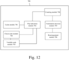
- FIG. 7 is a schematic structural diagram of a coder according to an example of the present disclosure.
- the coder 700 includes a cache module 701 and a flip indication module 702, wherein;
- the coder provided by the example of the present disclosure can be applied to the aforementioned memory system, and the coder 700 can be set in the decoding section of the memory controller as shown in FIG. 3 and configured to perform a coding operation on the codeword to be coded.
- the code word to be coded herein may refer to hard-read data, which may be read by the memory controller from the memory device according to a hard-read voltage, or the code word to be coded may also be the codeword flipped in a certain iteration during the coding. Whether the codeword to be coded is the hard-read data or the codeword flipped in a certain iteration will be described in detail in the subsequent description, and will not be repeated here.
- the hard-read voltage may be an initial read voltage, and the initial read voltage is the default read voltage preset by the memory system, which may be the same as a reference voltage in the Read Retry Table (RRT), or have a certain offset from the reference voltage, and the offset is included in the RRT.
- the hard-read voltage may also be an optimal read voltage.
- the way to obtain the optimal read voltage includes but is not limited to: determine the optimal read voltage according to the use of the memory device and the RRT.
- the specific process includes: traversing the RRT, determining a voltage offset in the RRT with the least error when reading memory device in this use case, and then obtaining the optimal read voltage based on the reference voltage and the determined voltage offset.
- the RRT is a table including multiple voltage offsets, wherein each voltage offset is relative to a reference voltage.
- These voltage offsets can be realized by hardware circuits in the memory. For example, these voltage offsets can be set through registers included in the memory. In other words, the required voltage offsets for all the read voltages are obtained based on the RRT table, and are then superimposed with the reference voltage (including the superposition of signs, that is, if the voltage offset is negative, the final read voltage is lower than the reference voltage) to obtain the required voltage value, which is then applied to the corresponding word line.
- RRT for example, as shown in Table 1, it is the RRT corresponding to a TLC type memory cell according to the example of the present disclosure.
- Each column in Table 1 represents a set of voltage offsets, i.e., Rd1 to Rd7, that distinguish adjacent programming states relative to the corresponding reference voltages. It should be noted that since the TLC type memory cell has 8 data states, it can be distinguished by using 7 read voltages, that is, there are 7 columns in Table 1.
- the set of voltage offsets described above may include a positive offset that increases toward a direction greater than the reference voltage, and a negative offset that decreases toward a direction smaller than the reference voltage.
- +V1, +V2, +V3, +V4 are positive offsets, wherein the values of V1, V2, V3, and V4 increase sequentially
- -V5 to -V11 are negative offsets, wherein the values of V5 to V11 decrease sequentially. Table 1.
- the soft data used in the coder can be a kind of probability information used to measure the reliability of certain read data (such as the hard-read data in the example of the present disclosure), which can be represented by a Log-Likelihood Ratio (LLR). Therefore, there will be read data as a benchmark for soft data to measure its reliability.
- LLR Log-Likelihood Ratio
- the hard-read data read with an optimal read voltage is 1100
- the data read with a first re-read voltage is 1000
- the first re-read voltage is on the left side of the optimal read voltage and deviates from the optimal read voltage with a certain offset, denoted as - ⁇
- the data read with a second re-read voltage is 1110, wherein the second re-read voltage is on the right side of the optimal read voltage and deviates from the optimal read voltage with a certain offset, denoted as + ⁇ .
- the soft data can be 0110.
- the soft data can be used to determine the reliability of the hard-read data 1100/1000/1110.
- the soft data is used to determine the reliability of the hard-read data, wherein the bit of "0" in the soft data indicates that the reliability of that bit in the hard-read data is relatively higher. In other words, that bit is determined to be closer to the truth.
- a bit of "1" in the soft data indicates that the reliability of that bit in the hard-read data is weaker.
- determination of the reliability of the hard-read data 1100 is done by using the soft data 0110, the leftmost bit of the hard-read data 1100 is "1", the number corresponding to that bit in the soft data is "0", and thus the reliability of that bit is relatively higher, that is, a strong "1".
- the middle two bits in the hard-read data 1100 correspond to “1 "s in the soft data, thus the reliability of the middle two bits is weaker, that is, weak "1” or "0", and the rightmost bit of the hard-read data 1100 is a strong "0".
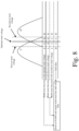
- the way of obtaining the soft data may include: as shown in FIG. 8 , directly reading the soft data from a NAND type memory device.
- the memory controller may send a command to read soft data to the memory device, and the memory device feeds back the soft data to the memory controller.
- the soft data may also be based on the XOR result of two adjacent hard-read data pre-cached in the memory of the memory controller.
- the coder When performing hard-decision coding on the codeword to be coded, the coder provided by the examples of the present disclosure obtains the soft data related to the codeword to be coded that is buffered by the buffer module in the coder, and then determines, with assistance of the soft data, a number of parity checks not satisfied by bits in the codeword to be coded.
- the hard-decision coding may be LDPC bit flip coding.
- LDPC bit-flip coding fast-read soft data is used to assist LDPC bit-flip coding at least in a first flip iteration, so as to greatly improve the correction capability of LDPC bit-flip coding.
- the use of soft data to assist bit flip determination at least in the first flip iteration may be done only in the first flip iteration, or in the first flip iteration and the second flip iteration, or in multiple flip iterations and so on.
- the parity checks not satisfied may mean that after the codeword to be coded is checked with the check matrix for a single time, each non-zero element in the generated checksum vector corresponds to that an equation of parity checks with which the bits in the codeword to be coded engage is not satisfied.
- the number of parity checks not satisfied by the bits in the codeword to be coded may refer to the number of equations of parity checks with which the bits in the codeword to be coded engage that are non-zero elements.
- the numbers of parity checks not satisfied by the bits in the codeword are respectively: C1: 2; C2: 2; C3: 0; C4: 1; C5: 2; C6: 1; C7:1; C8:0; C9:0; C10:1; C11:0; C12:1.
- the flip indication module 702 may further be configured to:
- this operation in some examples is to use soft data to assist in determining the number of parity checks not satisfied by the bits in the codeword to be coded.
- the initial error bit indication vector of the codeword to be coded is firstly determined.
- the initial error bit indication vector can refer to the number of parity checks not satisfied by the bits in the codeword to be coded when only LDPC bit flip coding is performed without using soft data assistance. Then, the number of parity checks not satisfied by the bits in the codeword to be coded is determined with assistance of the soft data in combination with the initial error bit indication vector.
- the flip indication module 702 is further configured to:
- the soft data is first expressed in the form of a soft data vector. Then, a sum operation is performed on the soft data vector and the aforementioned initial error bit indication vector to obtain a target error bit indication vector, wherein each element in the target error bit indication vector corresponds to the number of parity checks not satisfied by one bit.
- the initial error bit vector is: ⁇ 0, 1, 1, 0 ⁇
- the soft data vector corresponding to the soft data is ⁇ 0, 1, 1, 0 ⁇
- the target error bit vector is: ⁇ 0, 2, 2, 0 ⁇ .
- the number of parity checks not satisfied by the first bit in the codeword to be coded is 0, the number of parity checks not satisfied by the second bit in the codeword to be coded is 2, the number of parity checks not satisfied by the third bit in the codeword to be coded is 2, and the number of parity checks not satisfied by the fourth bit in the codeword to be coded is 0.
- the coder 700 further includes a variable node module 703 and a check node module 704.
- the node module and the check node module are connected to form a variable-check connection network according to a pre-constructed check matrix; wherein,
- the coder shown in FIG. 7 discloses only the main structures related to the inventive concepts of the examples of the present disclosure.
- the coder can further include a variable node module and a check node module.
- the variable node module can include multiple variable node units
- the check node module can include multiple check node units.
- the multiple variable node unit and multiple check node units are connected to form a variable-check connection network according to a pre-constructed check matrix.
- the pre-constructed check matrix may refer to an LDPC check matrix, also called an H matrix.
- variable-check connection network formed above can also be referred to as a Tanner graph, as shown in FIG. 10 .
- the Tanner graph includes a check node 1001, a variable node 1002 and an edge 1003 connecting the check node and the variable node.
- Check node information 1004A Values transferred from check nodes to variable nodes after check node processing are referred to as check node information 1004A.
- variable node information 1004B Values transferred from variable nodes to check nodes after variable node processing.
- the Tanner graph includes 5 check nodes 1001 of the parity check equation of the H matrix, 10 variable nodes 1002 representing code symbols, and edges 1003 representing the relationship between the check nodes and the variable nodes.
- the edge 1003 connects each check node to a variable node corresponding to a code symbol included in a parity check equation represented by the check node.
- FIG. 11 shows a Tanner graph formed by an H matrix, wherein the number of variable nodes connected to each check node is fixed at 4, and the number of check nodes connected to each variable node is fixed at 2.
- An initial value of a variable node can be hard-read data.
- the variable node module can receive hard-read data and generate the codeword to be coded according to the hard-read data, send the codeword to be coded to a check node module, and send the codeword to be coded and the hard-read data to the flip indication module.
- the check node module can receive the codeword to be coded, determine a checksum vector according to the codeword to be coded and the aforementioned check matrix, and send the checksum vector to the flip indication module.
- the flip indication module can receive the aforementioned codeword to be coded, hard-read data, checksum vector, obtain the check matrix, and then obtain the initial error bit indication vector according to the codeword to be coded, hard-read data, the checksum vector and the check matrix.
- the coder can be located in the decoding section of the memory controller. Therefore, the hard-read data received by the variable node module may be the read command in response to the processor. In this case, the read data fed back by the memory device via the memory I/F is directly transmitted to the variable node module via the bus. Alternatively, the hard-read data received by the variable node module may be the read command in response to the processor. In this case, the read data fed back by the memory device via the memory I/F is temporarily stored in the memory, and the hard-read data is obtained from the memory by the processor and transmitted to the variable node module. Any other processes that can obtain hard-read data are possible.
- the coder is inside the memory controller, and is coupled with other components such as the processor via a bus. Therefore, the variable node module can receive hard-read data from outside the coder. After the variable node module receives the hard-read data, the value of each bit of the hard-read data is assigned to the corresponding variable node unit to generate a codeword to be coded.
- Determining the checksum vector according to the codeword to be coded and the aforementioned check matrix may be implemented by multiplying the check matrix by the transposition of the codeword to be coded to obtain the checksum vector.
- the flip indication module 702 is further configured to:
- the first bit vector is obtained by performing a sum operation on the hard-read data (the codeword to be coded in the first iterative flip) and the codeword to be coded and then perform a modulo operation on the sum
- a second bit vector is obtained by multiplying transposition of the checksum vector by the check matrix
- the aforementioned initial error bit indication vector is obtained by performing a sum operation on the first bit vector and the second bit vector.
- the number of elements in the first bit vector and the second bit vector is the same as the number of bits in the codeword to be coded.
- f 1 y + y 0 mod 2 + s ′ H
- f1 is the initial error bit indication vector, and each element corresponds to a bit in the codeword to be coded
- y is the codeword to be coded
- y 0 is the hard-read data
- s' is the transposition of the checksum vector
- H is check matrix
- the codeword to be coded is the hard-read data
- the codeword to be coded is hard-read data after bit flipping.
- the flip indication module 702 is further configured to:
- the flipping criterion may include:
- the flip indication module obtains a flip indication vector according to the obtained number of parity checks not satisfied by each bit and the flipping criterion.
- the variable node module flips the bits to be flipped in the codeword to be coded according to the flip indication vector.
- the flipping criterion include but are not limited to flipping the bits in the codeword to be coded for which the number of parity checks not satisfied is largest, and flipping the bits in the codeword to be coded for which the number of parity checks not satisfied is greater than or equal to a preset threshold. In the above description, only the bit corresponding to the largest data in f2 is flipped; or alternatively, the bit whose data in f2 is greater than or equal to T (that is, the preset threshold) is flipped.
- the coder 700 further includes: a counting module 704 and a termination decision module 705, wherein,
- the number of flipping iterations is limited.
- the number of flipping iterations can be counted by the counting module 704, that is, the number of iterations is counted by the counting module.
- the termination decision module 705 determines whether the counted number of iterations reaches the maximum number of iterations and whether the checksum vector is a zero vector. When the maximum number of iterations is reached and the checksum vector is a non-zero vector, a first stop coding signal is output. The first stop coding signal is used to indicate that the hard-decision coding of the codeword to be coded fails.
- the coder 700 further includes: a rearrangement module 706;
- the termination decision module 705 outputs a second stop coding signal
- the rearrangement module in response to the second stop coding signal, performs rearrangement processing on the codeword to be coded, and outputs codeword to be coded in a correct order, so as to complete the coding of hard-read data.
- the termination decision module 705 is further configured to: when the checksum vector is not a zero vector and the number of iterations has not reached the maximum number of iterations, output a continue coding signal, and the continue coding signal is configured to: instruct the variable node module, the check node module and the flip indication module to continue to perform a hard-decision coding operation on the codeword to be coded.
- the operations here may refer to the terminating decision module outputting a continue coding signal when the checksum vector is not a zero vector and the number of iterations has not reached the maximum number of iterations.
- the continue coding signal is configured to indicate the aforementioned variable node module, the check node module and the flip indication module to continue to perform hard-decision coding operations on the codeword to be coded, so as to determine whether the coding of codeword to be coded succeeds or fails.
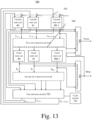
- FIG. 13 shows a schematic structural diagram of a coder according to an example of the present disclosure.
- d represents the hard-read data
- v represents the codeword to be coded
- S represents the checksum vector
- I represents the flip indication vector
- Stop is the stop coding signal, including the first stop coding signal and a second stop coding signal.
- a first sub-connection network and a second sub-connection network together form a variable-check node connection network.
- an implementable coding workflow can be as follows:
- the methods for obtaining the hard-read data and soft data in operation S1401 have been described above. That is, the hard-read data can be obtained by directly receiving feedback from the memory device or from the memory of the memory controller.
- the soft data can be cached into the cache module of the coder, and then obtained from the cache module.
- the above-mentioned operations are merely one way of implementing the coding workflow. The execution order of each operation can be adjusted according to the actual situation.
- S1404 can occur before S1402, and in this case, it is firstly determined whether the number of iterations reaches the maximum number of iterations, and if the maximum number of iterations has not reached, a checksum vector is generated by using check matrix and the codeword to be decoded; otherwise, outputting a coding failure indication signa, and ending the process.
- the soft data is applied to LDPC bit flipping (that is, hard-decision) coding.
- LDPC bit flipping that is, hard-decision
- the strong error correction capability of soft data is leveraged to speed up the LDPC bit flipping coding, so as to reduce the power consumed by LDPC bit flipping coding and improve the throughput of error correction of the coder.
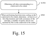
- An example of the present disclosure also provides a coding method, as shown in FIG. 15 , including:
- the determining, with assistance of the soft data, the number of parity checks not satisfied by the bits in the codeword to be coded comprises:
- the determining, with assistance of the soft data in combination with the initial error bit indication vector, the number of parity checks not satisfied by the bits in the codeword to be coded comprises:
- the determining the initial error bit indication vector corresponding to the codeword to be coded comprises:
- the determining the initial error bit indication vector corresponding to the codeword to be coded according to the hard-read data, the codeword to be coded, the checksum vector, and the check matrix comprises:
- the method further comprises:
- the flipping criterion comprises:
- the method further comprises:
- the method further comprises:
- the method further comprises: when the checksum vector is not a zero vector and the number of iterations has not reached the maximum number of iterations, output a continue coding signal, wherein the continue coding signal is configured to instruct to perform a hard-decision coding operation on the codeword to be coded.
- An example of the present disclosure further provides a memory controller 1600, as shown in FIG. 16 , including: a processor 1601 and the coder 700 described in any one of the above aspects, wherein the processor 1601 is configured to read soft data corresponding to a codeword to be coded from a memory device; the coder is configured to: cache the soft data; and when performing hard-decision coding on the codeword to be coded, determine, at least in a first flip iteration and with assistance of the soft data, a number of parity checks not satisfied by bits in the codeword to be coded.
- the memory controller provided by the example of the present disclosure includes the aforementioned coder, and therefore, the terms and features of the coder have been described in detail above, and will not be repeated here.
- An example of the present disclosure further provides a memory system, including:
- the processor is further configured to: read hard-read data from the memory device; and send the hard-read data to the coder; and the coder is further configured to: receive the hard-read data and generate the codeword to be coded according to the hard-read data.
- the coder includes: a cache module, a variable node module, a check node module, and a flip indication module, wherein;
- the memory system provided by the examples of the present disclosure includes the memory controller described above and the coder included in the memory controller. Therefore, reference may be made to the above description for the terms and features appearing herein, which will not be repeated here.
Landscapes
- Physics & Mathematics (AREA)
- Engineering & Computer Science (AREA)
- Theoretical Computer Science (AREA)
- Probability & Statistics with Applications (AREA)
- Mathematical Physics (AREA)
- General Engineering & Computer Science (AREA)
- General Physics & Mathematics (AREA)
- Microelectronics & Electronic Packaging (AREA)
- Quality & Reliability (AREA)
- Error Detection And Correction (AREA)
- Detection And Correction Of Errors (AREA)
- Memory System (AREA)
- Techniques For Improving Reliability Of Storages (AREA)
Abstract
Description
- The present disclosure relates to the field of memory technologies, and in particular to a coder, a coding method, a memory controller and a memory system.
- With the development of storage technology, 3D NAND flash memory (Flash) has evolved from Singe Level Cells (SLC) that can store 1 bit of information and Double Level Cells (DLC) that can store 2 bits of information to Triple Level Cells (TLC) that can store 3 bits of information, and even Quadruple Level Cells (QLC) that can store 4 bits of information. The number of stacked layers is also increasing. For memory devices with more and more layers and memory bits, low density parity check (LDPC) is usually employed for error correction when reading data in order to enhance the reliability of the data stored in the memory device. However, with the complex structure of 3D NAND Flash and more data it stores, the types of errors it contains become more and more complex. The current error correction methods suffer from the low error correction speed and the inefficiency, which seriously affects the reading rate.
- In view of this, the examples of the present disclosure provide a coder, a coding method, a memory controller and a memory system.
- To achieve the above object, technical solution of the present disclosure is achieved as follows.
- In a first aspect, an example of the present disclosure provides a coder comprising: a cache module and a flip indication module, wherein;
- the cache module is configured to cache soft data related to a codeword to be coded; and
- the flip indication module is configured to: obtain the soft data from the cache module, and when performing hard-decision coding on the codeword to be coded, determine, at least in a first flip iteration and with assistance of the soft data, a number of parity checks not satisfied by bits in the codeword to be coded.
- In the above solution, the flip indication module is further configured to:
- determine an initial error bit indication vector corresponding to the codeword to be coded; and
- determine, with assistance of the soft data in combination with the initial error bit indication vector, the number of parity checks not satisfied by the bits in the codeword to be coded.
- In the above solution, the coder further comprises a variable node module and a check node module that are connected to form a variable-check connection network according to a pre-constructed check matrix; wherein,
- the variable node module is configured to: receive hard-read data and generate the codeword to be coded according to the hard-read data; send the codeword to be coded to a check node module; and send the codeword to be coded and the hard-read data to the flip indication module;
- the check node module is configured to: receive the codeword to be coded; determine a checksum vector according to the codeword to be coded and the check matrix; and send the checksum vector to the flip indication module; and
- the flip indication module is further configured to: receive the codeword to be coded and the hard-read data sent by the variable node module; receive the checksum vector sent by the check node module; obtain the check matrix and the soft data; and determine the initial error bit indication vector corresponding to the codeword to be coded according to the hard-read data, the codeword to be coded, the checksum vector, and the check matrix.
- In the above solution, the flip indication module is further configured to:
- determine a soft data vector corresponding to the soft data;
- perform a sum operation on the soft data vector and the initial error bit indication vector to obtain a target error bit indication vector; and
- determine a number of parity checks not satisfied by each bit in the codeword to be coded according to the target error bit indication vector; and
- wherein each element in the target error bit indication vector corresponds to the number of parity checks not satisfied by one bit.
- In the above solution, the flip indication module is further configured to:
- perform a sum operation on the hard-read data and the codeword to be coded and then perform a modulo operation on the sum to obtain a first bit vector;
- multiply transposition of the checksum vector by the check matrix to obtain a second bit vector; and
- perform a sum operation on the first bit vector and the second bit vector to obtain the initial error bit indication vector.
- In the above solution, the flip indication module is further configured to:
- generate a flip indication vector according to the number of parity checks not satisfied and a flipping criterion, wherein the flip indication vector comprises determined bits that need to be flipped in the codeword to be coded; and
- the variable node module is further configured to: receive the flip indication vector, and flip the bits that need to be flipped in the codeword to be coded according to the flip indication vector.
- In the above solution, the flipping criterion comprises:
- flipping the bits in the codeword to be coded for which the number of parity checks not satisfied is largest; or
- flipping the bits in the codeword to be coded for which the number of parity checks not satisfied is greater than or equal to a preset threshold.
- In the above solution, the coder further comprises: a counting module and a termination decision module, wherein,
- the counting module is configured to: count a number of iterations of the hard-decision coding performed on the codeword to be coded; and
- the termination decision module is configured to: determine whether the number of iterations reaches a maximum number of iterations and determine whether the checksum vector is a zero vector; and when the number of iterations reaches the maximum number of iterations and the checksum vector is a non-zero vector, output a first stop coding signal, wherein the first stop coding signal is configured to indicate that the hard-decision coding of the codeword to be coded fails.
- In the above solution, the coder further comprises a rearrangement module;
- the termination decision module is further configured to: when it is determined that the checksum vector is a zero vector, output a second stop coding signal; and
- the rearrangement module is configured to: in response to the second stop coding signal, perform rearrangement processing on the codeword to be coded; and output codeword to be coded in a correct order.
- In the above solution, the termination decision module is further configured to: when the checksum vector is not a zero vector and the number of iterations has not reached the maximum number of iterations, output a continue coding signal, and the continue coding signal is configured to: instruct the variable node module, the check node module and the flip indication module to continue to perform a hard-decision coding operation on the codeword to be coded.
- In a second aspect, an example of the present disclosure provides a coding method, comprising:
- obtaining soft data corresponding to a codeword to be coded; and
- when performing hard-decision coding on the codeword to be coded, determining, at least in a first flip iteration and with assistance of the soft data, a number of parity checks not satisfied by bits in the codeword to be coded.
- In the above solution, the determining, with assistance of the soft data, the number of parity checks not satisfied by the bits in the codeword to be coded comprises:
- determining an initial error bit indication vector corresponding to the codeword to be coded; and
- determining, with assistance of the soft data in combination with the initial error bit indication vector, the number of parity checks not satisfied by the bits in the codeword to be coded.
- In the above solution, the determining, with assistance of the soft data in combination with the initial error bit indication vector, the number of parity checks not satisfied by the bits in the codeword to be coded comprises:
- determining a soft data vector corresponding to the soft data;
- performing a sum operation on the soft data vector and the initial error bit indication vector to obtain a target error bit indication vector;
- determining a number of parity checks not satisfied by each bit in the codeword to be coded according to the target error bit indication vector; and
- wherein each element in the target error bit indication vector corresponds to the number of parity checks not satisfied by one bit.
- In the above solution, the determining the initial error bit indication vector corresponding to the codeword to be coded comprises:
- receiving hard-read data and generating the codeword to be coded according to the hard-read data;
- determining a checksum vector according to the codeword to be coded and a pre-constructed check matrix; and
- determining the initial error bit indication vector corresponding to the codeword to be coded according to the hard-read data, the codeword to be coded, the checksum vector, and the check matrix.
- In the above solution, the determining the initial error bit indication vector corresponding to the codeword to be coded according to the hard-read data, the codeword to be coded, the checksum vector, and the check matrix comprises:
- performing a sum operation on the hard-read data and the codeword to be coded and then perform a modulo operation on the sum to obtain a first bit vector;
- multiplying transposition of the checksum vector by the check matrix to obtain a second bit vector; and
- performing a sum operation on the first bit vector and the second bit vector to obtain the initial error bit indication vector.
- In the above solution, the method further comprises:
- generating a flip indication vector according to the number of parity checks not satisfied and a flipping criterion, wherein the flip indication vector comprises determined bits that need to be flipped in the codeword to be coded; and
- flipping the bits that need to be flipped in the codeword to be coded according to the flip indication vector.
- In the above solution, the method further comprises:
- generating a flip indication vector according to the number of parity checks not satisfied and a flipping criterion, wherein the flip indication vector comprises determined bits that need to be flipped in the codeword to be coded; and
- flipping the bits that need to be flipped in the codeword to be coded according to the flip indication vector.
- In the above solution, the flipping criterion comprises:
- flipping the bits in the codeword to be coded for which the number of parity checks not satisfied is largest; or
- flipping the bits in the codeword to be coded for which the number of parity checks not satisfied is greater than or equal to a preset threshold.
- In the above solution, the method further comprises:
- counting a number of iterations of the hard-decision coding performed on the codeword to be coded;
- determining whether the number of iterations reaches a maximum number of iterations and determining whether the checksum vector is a zero vector; and
- when the number of iterations reaches the maximum number of iterations and the checksum vector is a non-zero vector, outputting a first stop coding signal, wherein the first stop coding signal is configured to indicate that the hard-decision coding of the codeword to be coded fails.
- In the above solution, the method further comprises:
- determining whether the checksum vector is a zero vector, and when it is determined that the checksum vector is a zero vector, outputting a second stop coding signal;
- in response to the second stop coding signal, performing rearrangement processing on the codeword to be coded; and outputting codeword to be coded in a correct order.
- In the above solution, the method further comprises:
when the checksum vector is not a zero vector and the number of iterations has not reached the maximum number of iterations, output a continue coding signal, wherein the continue coding signal is configured to instruct to perform a hard-decision coding operation on the codeword to be coded. - In a third aspect, an example of the present disclosure further provides a memory controller, comprising a processor and the coder according to any one of the above aspects, wherein the processor is configured to read soft data corresponding to a codeword to be coded from a memory device;
the coder is configured to: cache the soft data; and when performing hard-decision coding on the codeword to be coded, determine, at least in a first flip iteration and with assistance of the soft data, a number of parity checks not satisfied by bits in the codeword to be coded. - In a fourth aspect, an example of the present disclosure provides a memory system, comprising:
- a memory device configured to store data;
- a memory controller coupled to the memory device and comprising a processor and a coder; wherein the processor is configured to read soft data corresponding to a codeword to be coded from the memory device; and
- the coder is configured to: cache the soft data; and when performing hard-decision coding on the codeword to be coded, determine, at least in a first flip iteration and with assistance of the soft data, a number of parity checks not satisfied by bits in the codeword to be coded.
- In the above solution, the processor is further configured to: read hard-read data from the memory device; and send the hard-read data to the coder; and
the coder is further configured to: receive the hard-read data and generate the codeword to be coded according to the hard-read data. - In the above solution, the coder comprises: a cache module, a variable node module, a check node module, and a flip indication module, wherein,
- the cache module is configured to: cache the soft data read by the processor;
- the variable node module is configured to: receive the hard-read data read by the processor and generate the codeword to be coded according to the hard-read data; and send the codeword to be coded to a check node module;
- the check node module is configured to: receive the codeword to be coded sent by the variable node module; determine a checksum vector according to the codeword to be coded and a pre-constructed check matrix; and send the checksum vector to a flip indication module; and
- the flip indication module is configured to: receive the hard-read data and the codeword to be coded sent by the variable node module; receive the checksum vector sent by the check node module; obtain the check matrix and the soft data; determine an initial error bit indication vector corresponding to the codeword to be coded according to the hard-read data, the codeword to be coded, the checksum vector, and the check matrix; and determine, with assistance of the soft data in combination with the initial error bit indication vector, a number of parity checks not satisfied by bits in the codeword to be coded.
- Examples of the present disclosure provide a coder, a coding method, a memory controller, and a memory system. The coder comprises: a cache module and a flip indication module. The cache module is configured to cache soft data related to a codeword to be coded. The flip indication module is configured to: obtain the soft data from the cache module, and when performing hard-decision coding on the codeword to be coded, determine, at least in a first flip iteration and with assistance of the soft data, a number of parity checks not satisfied by bits in the codeword to be coded. The coder provided by the example of the present disclosure caches the soft data related to the codeword to be coded through the included buffer module, and then the flip indication module, when performing hard-decision coding on the codeword to be coded, determines, with assistance of the soft data, a number of parity checks not satisfied by bits in the codeword to be coded in one or more iterations. In this way, the soft data is used to assist the flipping decision of the hard-decision coding to enable high throughput and low power consumption of the hard-decision coding, greatly improving the error correction capability of hard-decision coding.
- In the drawings, which are not necessarily to scale, like reference numerals may describe similar components in the different views. The same number with a different letter suffix may indicate different instances of similar components. The drawings generally illustrate various examples discussed in this document, by way of example and not limitation.
-
FIG. 1 is a schematic diagram of an example system having a memory system according to an example of the present disclosure; -
FIG. 2a is a schematic diagram of an example memory card having a memory system according to an example of the present disclosure; -
FIG. 2b is a schematic diagram of an example solid state drive having a memory system according to an example of the present disclosure; -
FIG. 3 is a schematic structural diagram of a memory controller according to an example of the present disclosure; -
FIG. 4 is a schematic diagram of an example memory device including peripheral circuits according to an example of the present disclosure; -
FIG. 5 is a schematic cross-sectional view of a memory array including NAND type memory strings according to an example of the present disclosure; -
FIG. 6 is a schematic diagram of an example memory device including a memory array and peripheral circuits according to an example of the present disclosure; -
FIG. 7 is a schematic structural diagram of a coder according to an example of the present disclosure; -
FIG. 8 is an example schematic diagram of acquiring soft data and hard-read data according to an example of the present disclosure; -
FIG. 9 is a schematic structural diagram of a coder according to another example of the present disclosure; -
FIG. 10 is a schematic diagram of a Tanner graph according to an example of the present disclosure; -
FIG. 11 is a schematic diagram of a Tanner graph according to an example of the present disclosure; -
FIG. 12 is a schematic structural diagram of a coder according to another example of the present disclosure; -
FIG. 13 is a schematic structural diagram of a coder according to another example of the present disclosure; -
FIG. 14 is a schematic diagram of a workflow of a coder according to an example of the present disclosure; -
FIG. 15 is a schematic flowchart of a coding method according to an example of the present disclosure; and -
FIG. 16 is a schematic structural diagram of a memory controller according to an example of the present disclosure. - Various examples of the present disclosure are described in more detail below with reference to the accompanying drawings. Other examples that are variations of any disclosed example can be formed by differently configuring or arranging elements and features of the examples of the present disclosure. Therefore, examples of the present disclosure are not limited to the examples set forth herein. Rather, the described examples are provided so that the disclosed examples will be thorough and complete, and will fully convey the scope of the disclosed examples to those skilled in the art to which the examples of the present disclosure pertain. It should be noted that references to "an example," "another example," and the like do not necessarily mean only one example, and that different references to any such phrase are not necessarily directed to the same example. It should be understood that although the terms such as "first," "second," "third," etc. may be used herein to identify various elements, these elements should not be limited by these terms. These terms are used to distinguish one element from another element having the same or similar name. Therefore, a first element in one example may also be referred to as a second or third element in another example without departing from the spirit and scope of the examples of the present disclosure.
- The drawings are not necessarily to scale, and in some instances the scale may have been exaggerated to clearly illustrate features of the examples. When an element is referred to as being connected or coupled to another element, it should be understood that the former may be directly connected or coupled to the latter or electrically connected or coupled to the latter via one or more intervening elements therebetween. In addition, it will also be understood that when an element is referred to as being "between" two elements, it may be the only element between the two elements, or one or more intervening elements may also be present.
- The terminology used herein is for the purpose of describing particular examples only and is not intended to be limiting of the present disclosure. As used herein, singular forms are intended to include plural forms unless the context clearly dictates otherwise. Unless otherwise stated or clearly understood as a singular form from the context, at least one of the articles "a" or "an" used in the examples of the present disclosure and the appended claims shall be collectively interpreted as meaning "one or more". It should be further understood that the terms "comprise", "comprising", "include" and "including" used in the examples of the present disclosure specify the presence of stated elements and do not exclude the presence or addition of one or more other elements. The term "at least one of" used in the examples of the present disclosure includes any and all combinations of one or more of the associated listed items. Unless otherwise defined, all terms including technical and scientific terms used in the examples of the present disclosure have the same meanings as commonly understood by one of ordinary skill in the art to which the present disclosure belongs in view of the examples of the present disclosure. It should be further understood that, unless clearly defined by the examples of the present disclosure, terms such as those defined in commonly used dictionaries should be interpreted as having meanings consistent with their meanings in the context of the examples of the present disclosure and related technologies, and should not be interpreted in an ideal or overly formalized way.
- In the following description, numerous specific details are set forth in order to provide a thorough understanding of the disclosure, and the disclosure may be practiced without some or all of these specific details. In other instances, at least one of well-known processing structures or processes have not been described in detail so as not to unnecessarily obscure the present disclosure. It should also be understood that in some cases, unless stated otherwise, a feature or element described with respect to one example may be used alone or in combination with other features or elements of another example, unless otherwise specified, as would be apparent to a person skilled in the relevant art. Hereinafter, various examples of the present disclosure are described in detail with reference to the accompanying drawings. The following description focuses on details to facilitate understanding of examples of the present disclosure. Well-known technical details may be omitted so as not to obscure the features and aspects of the examples of the present disclosure.
- To understand the characteristics and technical content of the examples of the present disclosure in more detail, the examples of the present disclosure are described in detail below in conjunction with the accompanying drawings. The appended drawings are only for reference and description, and are not intended to limit the examples of the present disclosure.
- A memory device is memory equipment used to preserve information in modern information technology. As a typical non-volatile memory device, 3D NAND (Not-And) type memory device has become a mainstream product in the storage market due to its high storage density, controllable production cost, suitable programming and erasing speed and retention characteristics. With the increase in the number of memory bits of the memory cell and the increase in the number of stacked layers, the types of errors that occur during the read operation of the memory device become more and more complex. In this case, when LDPC hard-decision coding in the coder is used to code the codeword to be coded (data read from the memory device), the coding time is longer and the error correction capability is weaker, which seriously affects the reading rate.
- Based on one or more of the above problems, an example of the present disclosure provides a coder that utilizes soft data to assist the flip decision of hard-decision coding, and realizes the characteristics of high throughput and low power consumption of hard-decision coding, thus greatly improving he error correction capability of hard-decision coding.
- The examples of the present disclosure will be further described in detail below in conjunction with the accompanying drawings and specific examples.
-
FIG. 1 is a schematic diagram of an example system having a memory system according to an example of the present disclosure. InFIG. 1 , thesystem 100 can be a mobile phone, a desktop computer, a laptop computer, a tablet, a vehicle computer, a gaming console, a printer, a positioning device, a wearable electronic device, a smart sensor, a virtual reality (VR) device, an argument reality (AR) device, or any other suitable electronic devices having a memory system therein. As shown inFIG. 1 ,system 100 can include ahost 108 and amemory system 102. Thehost 108 may include a processor, such as a Central Processing Unit (CPU) or a System of Chip (SoC). The SoC may be, for example, an Application Processor (AP). Thehost 108 further includes at least one operating system (OS) that can generally manage and control the functions and operations performed in thehost 108. The OS may enable interoperability between ahost 108 coupled to thememory system 102 and users who need and use thememory system 102. The OS may support functions and operations corresponding to user's requests. By way of example but without limitation, according to whether the type of thehost 102 is a removable host, the OS may be classified into a general-purpose operating system and a mobile operating system. The general-purpose operating system can include personal operating systems, which may be an operating system that is used to support services for general purpose including Windows and Chrome, and enterprise operating systems, which may be an operating system specially designed to ensure and support high performance including Windows Server, Linux, Unix, etc. The mobile operating system may refer to an operating system for mobility services or functions (e.g., power saving function). Generally speaking, the mobile operating system may be an operating system such as Android, iOS, and Windows Mobile. In some examples, thehost 108 may include multiple Oss. Correspondingly, thehost 108 may run multiple operating systems related to thememory system 102. In other examples, thehost 108 converts the user's request into one or more commands, and transmits the one or more commands to thememory system 102, so that thememory system 102 executes operations related to the one or more commands. - The
memory system 102 is capable of operating or performing specific functions or performing various internal operations in response to a request from thehost 108. In some examples, thememory system 102 is capable of storing data accessed by thehost 108. Thememory system 102 can function as a primary memory system or a secondary memory system for thehost 108. Thememory system 102 and thehost 108 can be electrically coupled and communicate according to corresponding protocols. Thememory system 102 can be implemented and packaged into different types of end electronic products, including, but not limited to: Solid State Drive (SSD), Multimedia Card (MMC), Embedded MMC (eMMC), Reduced Size MMC (RSMMC), Micro MMC, Secure Digital (SD) cards, Mini SD, Micro SD, Universal Serial Bus (USB) storage devices, Universal Flash Memory (UFS) devices, Compact Flash (CF) cards, Smart Media (SM) cards and memory sticks, and so on. - In some examples, the
memory system 102 may also be configured as part of, for example, computers, ultra-mobile PCs (UMPCs), workstations, netbooks, personal digital assistants (PDAs), portable computers, web tablets, tablet computers, wireless phones, mobile phones, smart phones, e-books, portable multimedia players (PMPs), portable game consoles, navigation systems, black boxes, digital cameras, digital multimedia broadcasting (DMB) players, three-dimensional (3D) televisions, smart TVs, digital audio recorders, digital audio players, digital picture recorders, digital picture players, digital video recorders, digital video players, storage devices configured with a data center, devices capable of transmitting and receiving information in a wireless environment, one of various electronic devices configured with a home network, one of various electronic devices configured with a computer network, one of various electronic devices configured with telematics network, radio frequency identification (RFID) devices, or one of the various components configured with a computing system. - Referring back to
FIG. 1 , thememory system 102 may include one ormore memory devices 104 and amemory controller 106. Thememory controller 106 can respond to the request of thehost 108, and then control thememory device 104. For example, thememory controller 106 can read data from thememory device 104, and transmit the read data to thehost 108. Furthermore, thememory controller 106 can receive data to be stored from thehost 108, and store the data to be stored into thememory device 104. That is, thememory controller 106 is capable of controlling write (or program) operations, read operations, erase operations, background operations, and the like of thememory device 104. Furthermore, thememory system 102 can be implemented and packaged into different types of end electronic products. In one example as shown inFIG. 2 a ,memory controller 106 and asingle memory device 104 may be integrated intomemory card 202.Memory card 202 can include a PC card (PCMCIA, personal computer memory card international association), a CF card, a smart media (SM) card, a memory stick, a multimedia card (MMC, RS-MMC, MMCmicro), an SD card (SD, miniSD, microSD, SDHC), a UFS, etc.Memory card 202 can further include amemory card connector 204coupling memory card 202 with a host (e.g., host 108 inFIG. 1 ). In another example as shown inFIG. 2b ,memory controller 206 andmultiple memory devices 104 may be integrated into anSSD 206.SSD 206 can further include anSSD connector 208coupling SSD 206 with a host (e.g., host 108 inFIG. 1 ). In some examples, at least one of the storage capacity or the operation speed ofSSD 206 is greater than those ofmemory card 202. - As shown in
FIG. 3 , thememory controller 106 may include a host I/F (or front-end interface) 301, a memory I/F (or back-end interface) 302, aprocessor 303, and amemory 304. The above-mentionedcomponents memory controller 106 in thememory controller 106 can share transmission signals inside thememory controller 106 through an internal bus. In some examples, the host I/F 301 can interface thehost 108 with thememory system 102 in response to the protocol ofhost 108, and the host I/F 301 exchanges transfer commands and data operations between thehost 108 and thememory system 102. The host I/F 301 can process commands and data sent by thehost 108, and can include at least one of the followings: Universal Serial Bus (USB), Multimedia Card (MMC), Peripheral Component Interconnect Express (PCI-e or PCIe), Small Computer System Interface (SCSI), Serial SCSI (SAS), Serial Advanced Technology Attachment (SATA), Parallel Advanced Technology Attachment (PATA), Small Computer System Interface (SCSI), Enhanced Small Disk Interface (ESDI), and Electronics Integration drive (IDE). In some examples, the host I/F 301 is a component of thememory system 102 used to exchange data with thehost 108 and may be implemented by firmware called a host interface layer (HIL). - The memory I/
F 302 may be an interface for commands and data transferred betweenmemory controller 106 andmemory device 104, allowingmemory controller 106 to control thememory device 104 in response to requests communicated from thehost 108. The memory I/F 302 may generate control signals for controlling thememory device 104. In some examples, if thememory device 104 is a NAND flash memory, the memory I/F 302 can write data into thememory device 104 or read data from thememory device 104 under the control of theprocessor 303. The memory I/F 302 can handle commands and data between thememory controller 106 and thememory device 104, for example, the operation of the NAND flash interface, especially the operation between thememory controller 106 and thememory device 104. According to an example, the memory I/F 302 may be implemented as a component for exchanging data with thememory device 104 by firmware called a Flash Interface Layer (FIL). - The
processor 303 may be implemented by a microprocessor or a central processing unit (CPU). Thememory system 102 may include one ormore processors 303. Theprocessor 303 can control the overall operation of thememory system 102. By way of example and not limitation, theprocessor 303 may control a program operation or a read operation of thememory device 104 in response to a write request or a read request from thehost 108. According to an example, theprocessor 303 may use or run firmware to control the overall operation of thememory system 102. In this disclosure, firmware may be referred to as a flash translation layer (FTL). The FTL may operate as an interface between thehost 108 and thememory device 104. Thehost 108 can transmit requests related to write operations and read operations to thememory device 104 through the FTL. For example, thememory controller 106 uses theprocessor 303 when performing an operation requested from thehost 108 in thememory device 104. Theprocessor 303 coupled tomemory device 104 may process instructions or commands related to commands from thehost 108. Thememory controller 106 can perform a foreground operation such as a command operation corresponding to a command input from thehost 108, for example, a program operation corresponding to a write command, a read operation corresponding to a read command, and an erase/discard operation corresponding to an erase/discard command, and a parameter setting operation corresponding to a set parameter command or a set feature command with a set command. - As another example, the
memory controller 106 may perform background operations on thememory device 104 by theprocessor 303. By way of example and not limitation, the background operations may include garbage collection (GC) operations, wear leveling (WL) operations, map clear operations, and bad block management operations that check or search for bad blocks. The garbage collection operations may include operations to copy and process data stored in a certain memory block in thememory device 104 to another memory block. The wear leveling operations may include operations to swap and process stored data between memory blocks of thememory device 104. The map clear operations may include operations to store map data stored in thememory controller 106 into memory blocks of thememory device 104. The bad block management operations may include operations to check and process bad blocks in memory blocks of thememory device 104. Thememory controller 106 may respond to operations to access memory blocks of thememory device 104. The operations to access the memory blocks of thememory device 104 may include foreground or background operations performed on the memory blocks of thememory device 104. - The
memory 304 may be a working memory of thememory controller 106 and is configured to store data used to drive thememory controller 106. More specifically, when thememory controller 106 controls thememory device 104 in response to a request from thehost 108, thememory 304 can store firmware driven by theprocessor 303 and data (e.g., metadata) required to drive the firmware. Thememory 304 may also be a buffer memory of thememory controller 106 and is configured to temporarily store the write data transferred from thehost 108 to thememory device 104 and the read data transferred from thememory device 104 to thehost 108. Thememory 304 may include program memory, data memory, write buffer/cache, read buffer/cache, data buffer/cache, and map buffer/cache for storing the write data and the read data. Thememory 304 may be implemented using volatile memory. Thememory 304 may be implemented using static random access memory (SRAM), dynamic random access memory (DRAM), or both. - Although
FIG. 3 shows thememory 304 being included in thememory controller 106, the present disclosure is limited thereto. In an example, thememory 304 may be external to thememory controller 106, and thememory controller 106 may input and output data to and frommemory 304 via a separate memory interface (not shown). - An error correction (ECC)
module 305 is provided with an encoding section 3051 and a decoding section 3052. The encoding section 3051 can perform an encoding operation such as LDPC on data to be programmed into thesemiconductor memory device 104, and output data including an additional parity check bit. The parity check bit may be stored in thesemiconductor memory device 104. The decoding section 3052 can perform error correction decoding on the data read from thesemiconductor memory device 104, determine whether the error correction decoding is successful, output an instruction signal based on the determination result, and use the parity check bit generated by the LDPC encoding operation to correct error bits of data. - Here, although
FIG. 3 shows that theerror correction module 305 is included in thememory controller 106, the present disclosure is not limited thereto. In an example, theerror correction module 305 may be external to thememory controller 106, and thememory controller 106 may be in data communication with theerror correction module 305 via a separate interface (not shown). - Referring back to
FIG. 1 , thememory device 104 may include non-volatile memory that retains data stored therein even when power is not supplied. Thememory device 104 may further include volatile storage memory. Thedevice 104 can store data provided from thehost 108 through a write operation. Thememory device 104 can also provide the stored data to thehost 108 through a read operation. In examples of the present disclosure, thememory device 104 may include any memory disclosed, for example, volatile memory devices such as dynamic random access memory (DRAM) and static RAM (SRAM), or non-volatile memory devices such as Read-Only Memory (ROM), Mask ROM (MROM), Programmable ROM (PROM), Erasable Programmable ROM (EPROM), Electrically Erasable Programmable ROM (EEPROM), Ferroelectric RAM (FRAM), Phase Change RAM (PRAM), Magnetic Resistive RAM (MRAM), Resistive RAM (RRAM or ReRAM), and flash memory (such as three-dimensional NAND flash memory). - The memory device is illustrated by taking a three-dimensional NAND flash memory as an example. Referring to
FIG. 4 , it shows a schematic circuit diagram of anexample memory device 400 including peripheral circuits according to some aspects of the present disclosure. Thememory device 400 may be an example of thememory device 104 inFIG. 1 . Thememory device 400 may include amemory array 401 and aperipheral circuit 402 coupled to thememory array 401. Thememory array 401 is illustrated by taking a three-dimensional NAND type memory array as an example. Thememory cells 406 are provided in the form of an array ofNAND memory strings 408 each extending vertically above a substrate (not shown). In some examples, eachNAND memory string 408 includes a plurality ofmemory cells 406 coupled in series and stacked vertically. Eachmemory cell 406 can hold a continuous, analog value, such as an electrical voltage or charge, that depends on the number of electrons trapped within a region ofmemory cell 406. Eachmemory cell 406 can be either a floating gate type of memory cell including a floating-gate transistor or a charge trap type of memory cell including a charge trap transistor. - In some examples, each
memory cell 406 is a single-level cell (SLC) that has two possible memory states and thus, can store one bit of data. For example, the first memory state "0" can correspond to a first range of voltages, and the second memory state "1" can correspond to a second range of voltages. In some examples, eachmemory cell 406 is a multi-level cell (MLC) that is capable of storing more than a single bit of data in more than four memory states. For example, the MLC can store two bits per cell, three bits per cell (also known as trinary-level cell (TLC)), four bits per cell (also known as a quad-level cell (QLC)), or five bits per cell (also known as a penta-level cell (PLC)). Each MLC can be programmed to assume a range of possible nominal storage values. In one example, if each MLC stores two bits of data, then the MLC can be programmed to assume one of three possible programming levels from an erased state by writing one of three possible nominal storage values to the cell. A fourth nominal storage value can be used for the erased state. - As shown in
FIG. 4 , eachNAND memory string 408 can include a bottom selective gate (BSG) 410 at its source end and a top selective gate (TSG) 412 at its drain end.BSG 410 andTSG 412 can be configured to activate selectedNAND memory strings 408 during read and program operations. In some examples, the sources ofNAND memory strings 408 in asame block 404 are coupled through a same source line (SL) 414, e.g., a common SL. In other words, allNAND memory strings 408 in thesame block 404 have an array common source (ACS), according to some examples.TSG 412 of eachNAND memory string 408 is coupled to a respective bit line (BL) 416 from which data can be read or written via an output bus (not shown), according to some examples. In some examples, eachNAND memory string 408 is configured to be selected or deselected by at least one of applying a select voltage (e.g., above the threshold voltage of the transistor having TSG 412) or a deselect voltage (e.g., 0 V) torespective TSG 412 through one ormore TSG lines 413 or applying a select voltage (e.g., above the threshold voltage of the transistor having BSG 410) or a deselect voltage (e.g., 0 V) torespective BSG 410 through one or more BSG lines 415. - As shown in
FIG. 4 ,NAND memory strings 408 can be organized intomultiple blocks 404, each of which can have acommon source line 414, e.g., coupled to the ground. In some examples, eachblock 404 is the basic data unit for erase operations, i.e., allmemory cells 406 on thesame block 404 are erased at the same time. To erasememory cells 406 in a selectedblock 404,source lines 414 coupled to selectedblock 404 as well asunselected blocks 404 in the same plane as selectedblock 404 can be biased with an erase voltage (Vers), such as a high positive voltage (e.g., 20 V or more). It is understood that in some examples, erase operations may be performed at a half-block level, a quarter-block level, or a level having any suitable number of blocks or any suitable fractions of a block.Memory cells 406 of adjacentNAND memory strings 408 can be coupled throughword lines 418 that select which row ofmemory cells 406 is affected by read and program operations. -
FIG. 5 shows a schematic cross-sectional view of anexample memory array 401 includingNAND memory strings 408 in accordance with some aspects of the present disclosure. As shown inFIG. 5 , theNAND memory string 408 may include astacked structure 510, which includes a plurality of gate layers 511 and a plurality of insulatinglayers 512 alternately stacked in sequence, and amemory string 408 vertically penetrating through the gate layers 511 and the insulating layers 512. Thegate layer 511 and the insulatinglayer 512 can be stacked alternately, and two adjacent gate layers 511 are separated by an insulatinglayer 512. The number of pairs of gate layers 511 and insulatinglayers 512 in thestacked structure 510 can determine the number of memory cells included in thememory array 401. - The constituent material of the
gate layer 511 may include a conductive material. The conductive material may include but is not limited to tungsten (W), cobalt (Co), Copper (Cu), aluminum (Al), polysilicon, doped silicon, silicide, or any combination thereof. In some examples, eachgate layer 511 may include a metal layer, e.g., a tungsten layer. In some examples, eachgate layer 511 includes a doped polysilicon layer. Eachgate layer 511 may include a control gate surrounding the memory cell. Thegate layer 511 at the top of the stackedstructure 510 may extend laterally as a top selective gate line, thegate layer 511 at the bottom of the stackedstructure 510 may extend laterally as a bottom selective gate line, and thegate layer 511 extending laterally between the top selective gate line and the bottom selective gate line may be used as aword line layer 503. - In some examples, the
stacked structure 510 may be disposed on asubstrate 501. Thesubstrate 501 may include silicon (e.g., monocrystalline silicon), silicon germanium (SiGe), gallium arsenide (GaAs), germanium (Ge), silicon-on-insulator (SOI), germanium-on-insulator (GOI), or any other suitable material. - In some examples,
NAND memory string 408 includes a channel structure extending vertically through thestacked structure 510. In some examples, the channel structure includes a channel hole filled with semiconductor material(s) (e.g., as a semiconductor channel) and dielectric material(s) (e.g., as a memory film). In some examples, the semiconductor channel includes silicon, e.g., polysilicon. In some examples, the memory film is a composite dielectric layer including a tunneling layer, a storage layer (also referred to as a "charge trap/storage layer"), and a blocking layer. The channel structure may have a cylindrical shape (e.g., a pillar shape). According to some examples, the semiconductor channel, the tunneling layer, the storage layer and the blocking layer are radially arranged in this order from the center of the pillar toward the outer surface of the pillar. The tunneling layer may include silicon oxide, silicon oxynitride, or any combination thereof. The storage layer may include silicon nitride, silicon oxynitride, or any combination thereof. The blocking layer may include silicon oxide, silicon oxynitride, a high dielectric constant (high-k) dielectric, or any combination thereof. In one example, the memory film may include a composite layer of silicon oxide/silicon oxynitride/silicon oxide (ONO). - Referring back to
FIG. 4 ,peripheral circuits 402 can be coupled tomemory array 401 throughbit lines 416, word lines 418, source lines 414,BSG lines 415, andTSG lines 413.Peripheral circuits 402 can include any suitable analog, digital, and mixed-signal circuits for facilitating the operations ofmemory array 401 by applying and sensing at least one of voltage signals or current signals to and from eachtarget memory cell 406 throughbit lines 416, word lines 418, source lines 414,BSG lines 415, andTSG lines 413.Peripheral circuits 402 can include various types of circuits formed using metal-oxide-semiconductor (MOS) technologies. For example,FIG. 6 illustrates some example peripheral circuits, theperipheral circuits 402 including a page buffer/sense amplifier 604, a column decoder/bit line driver 606, a row decoder/word line driver 608, avoltage generator 610,control logic 612, registers 614, aninterface 616, and adata bus 618. It is understood that in some examples, additional peripheral circuits not shown inFIG. 6 may be included as well. - Page buffer/
sense amplifier 604 can be configured to read and program (write) data from and tomemory array 401 according to the control signals fromcontrol logic 612. In one example, page buffer/sense amplifier 604 may store program data (write data) to be programmed intomemory array 401. In another example, page buffer/sense amplifier 604 may perform program verify operations to ensure that the data has been properly programmed intomemory cells 406 coupled to selected word lines 418. In still another example, page buffer/sense amplifier 604 may also sense the low power signals frombit line 416 that represents a data bit stored inmemory cell 406 and amplify the small voltage swing to recognizable logic levels in a read operation. Column decoder/bit line driver 606 can be configured to be controlled bycontrol logic 612 and select one or moreNAND memory strings 408 by applying bit line voltages generated fromvoltage generator 610. - Row decoder/
word line driver 608 can be configured to be controlled bycontrol logic 612 and select/deselect blocks 404 ofmemory array 401 and select/deselectword lines 418 ofblock 404. Row decoder/word line driver 608 can be further configured to driveword lines 418 using word line voltages generated fromvoltage generator 610. In some examples, row decoder/word line driver 608 can also select/deselect and driveBSG lines 415 andTSG lines 413 as well. Row decoder/word line driver 608 is configured to perform program operations on thememory cells 406 coupled to the selected word line(s) 418.Voltage generator 610 can be configured to be controlled bycontrol logic 612 and generate the word line voltages (e.g., read voltage, program voltage, pass voltage, channel boost voltage, verification voltage, etc.), bit line voltages, and source line voltages to be supplied tomemory array 401. -
Control logic 612 can be coupled to each peripheral circuit described above, such asvoltage generator 610, row decoder/word line driver 608, etc., and configured to control operations of each peripheral circuit.Registers 614 can be coupled to controllogic 612 and include status registers, command registers, and address registers for storing status information, command operation codes (OP codes), and command addresses for controlling the operations of each peripheral circuit.Interface 616 may be coupled to controllogic 612 and act as a control buffer to buffer and relay control commands received from a host (not shown) to controllogic 612, and to buffer and relay status information received fromcontrol logic 612 to the host.Interface 616 may further be coupled to column decoder/bit line driver 606 viadata bus 618 and act as a data I/O interface and data buffer to buffer and relay data to or frommemory array 401. - Among 3D NAND type memory devices, Single-Level Cell (SLC) occupies a certain share in the memory market due to its advantages such as fast read and write speed, high reliability and long service life, whereas Multi-Level Cell (MLC), Trinary-Level Cell (TLC) and Quad-Level Cell (QLC) have become the development trend of the memory market due to their higher storage density and larger storage capacity.
- However, as the number of memory bits of the memory cell increases and the number of stacked layers increases, the types of errors it contains become more and more complex. When performing a read operation on the memory device, LDPC hard-decision coding is used to code the codeword to be coded, the coding time is longer, and the error correction ability is weak, which seriously affects the reading rate.
- Based on the memory device and memory system described above, in order to solve one or more of the above-mentioned problems, reference is made to
FIG. 7. FIG. 7 is a schematic structural diagram of a coder according to an example of the present disclosure. - In some examples, the
coder 700 includes acache module 701 and aflip indication module 702, wherein; - the
cache module 701 is configured to cache soft data related to the codeword to be coded; - the
flip indication module 702 is configured to: obtain the soft data from thecache module 701, and when performing hard-decision coding on the codeword to be coded, determine, at least in a first flip iteration and with assistance of the soft data, a number of parity checks not satisfied by bits in the codeword to be coded. - It should be noted that the coder provided by the example of the present disclosure can be applied to the aforementioned memory system, and the
coder 700 can be set in the decoding section of the memory controller as shown inFIG. 3 and configured to perform a coding operation on the codeword to be coded. The code word to be coded herein may refer to hard-read data, which may be read by the memory controller from the memory device according to a hard-read voltage, or the code word to be coded may also be the codeword flipped in a certain iteration during the coding. Whether the codeword to be coded is the hard-read data or the codeword flipped in a certain iteration will be described in detail in the subsequent description, and will not be repeated here. - Here, the hard-read voltage may be an initial read voltage, and the initial read voltage is the default read voltage preset by the memory system, which may be the same as a reference voltage in the Read Retry Table (RRT), or have a certain offset from the reference voltage, and the offset is included in the RRT. Alternatively, the hard-read voltage may also be an optimal read voltage. The way to obtain the optimal read voltage includes but is not limited to: determine the optimal read voltage according to the use of the memory device and the RRT. The specific process includes: traversing the RRT, determining a voltage offset in the RRT with the least error when reading memory device in this use case, and then obtaining the optimal read voltage based on the reference voltage and the determined voltage offset.
- It should be noted that the RRT is a table including multiple voltage offsets, wherein each voltage offset is relative to a reference voltage. These voltage offsets can be realized by hardware circuits in the memory. For example, these voltage offsets can be set through registers included in the memory. In other words, the required voltage offsets for all the read voltages are obtained based on the RRT table, and are then superimposed with the reference voltage (including the superposition of signs, that is, if the voltage offset is negative, the final read voltage is lower than the reference voltage) to obtain the required voltage value, which is then applied to the corresponding word line.
- For the RRT, for example, as shown in Table 1, it is the RRT corresponding to a TLC type memory cell according to the example of the present disclosure. Each column in Table 1 represents a set of voltage offsets, i.e., Rd1 to Rd7, that distinguish adjacent programming states relative to the corresponding reference voltages. It should be noted that since the TLC type memory cell has 8 data states, it can be distinguished by using 7 read voltages, that is, there are 7 columns in Table 1.
- The set of voltage offsets described above may include a positive offset that increases toward a direction greater than the reference voltage, and a negative offset that decreases toward a direction smaller than the reference voltage. For example, for Rd7, +V1, +V2, +V3, +V4 are positive offsets, wherein the values of V1, V2, V3, and V4 increase sequentially, whereas -V5 to -V11 are negative offsets, wherein the values of V5 to V11 decrease sequentially.
Table 1. RRT Rd1 Rd2 Rd3 Rd4 Rd5 Rd6 Rd7 -- -- -- -- -- -- 0 -- -- -- -- -- -- +V1 -- -- -- -- -- -- +V2 -- -- -- -- -- -- +V3 -- -- -- -- -- -- +V4 -- -- -- -- -- -- -V5 -- -- -- -- -- -- -V6 -- -- -- -- -- -- -V7 -- -- -- -- -- -- -V8 -- -- -- -- -- -- -V9 -- -- -- -- -- -- -V10 -- -- -- -- -- -- -V11 - Returning to the coder shown in
FIG. 7 , the soft data used in the coder can be a kind of probability information used to measure the reliability of certain read data (such as the hard-read data in the example of the present disclosure), which can be represented by a Log-Likelihood Ratio (LLR). Therefore, there will be read data as a benchmark for soft data to measure its reliability. - Reference may be made to
FIG. 8 for the soft data. InFIG. 8 , it is assumed that the hard-read data read with an optimal read voltage is 1100, the data read with a first re-read voltage is 1000, wherein the first re-read voltage is on the left side of the optimal read voltage and deviates from the optimal read voltage with a certain offset, denoted as -Δ, and the data read with a second re-read voltage is 1110, wherein the second re-read voltage is on the right side of the optimal read voltage and deviates from the optimal read voltage with a certain offset, denoted as +Δ. Correspondingly, the soft data can be 0110. In this case, the soft data can be used to determine the reliability of the hard-read data 1100/1000/1110. In some examples, the soft data is used to determine the reliability of the hard-read data, wherein the bit of "0" in the soft data indicates that the reliability of that bit in the hard-read data is relatively higher. In other words, that bit is determined to be closer to the truth. A bit of "1" in the soft data indicates that the reliability of that bit in the hard-read data is weaker. For example, inFIG. 8 , determination of the reliability of the hard-read data 1100 is done by using the soft data 0110, the leftmost bit of the hard-read data 1100 is "1", the number corresponding to that bit in the soft data is "0", and thus the reliability of that bit is relatively higher, that is, a strong "1". By analogy, the middle two bits in the hard-read data 1100 correspond to "1 "s in the soft data, thus the reliability of the middle two bits is weaker, that is, weak "1" or "0", and the rightmost bit of the hard-read data 1100 is a strong "0". - In some examples, the way of obtaining the soft data may include: as shown in
FIG. 8 , directly reading the soft data from a NAND type memory device. In some examples, the memory controller may send a command to read soft data to the memory device, and the memory device feeds back the soft data to the memory controller. In some other examples, the soft data may also be based on the XOR result of two adjacent hard-read data pre-cached in the memory of the memory controller. - When performing hard-decision coding on the codeword to be coded, the coder provided by the examples of the present disclosure obtains the soft data related to the codeword to be coded that is buffered by the buffer module in the coder, and then determines, with assistance of the soft data, a number of parity checks not satisfied by bits in the codeword to be coded. The hard-decision coding may be LDPC bit flip coding. In LDPC bit-flip coding, fast-read soft data is used to assist LDPC bit-flip coding at least in a first flip iteration, so as to greatly improve the correction capability of LDPC bit-flip coding. The use of soft data to assist bit flip determination at least in the first flip iteration may be done only in the first flip iteration, or in the first flip iteration and the second flip iteration, or in multiple flip iterations and so on.
- Here, the parity checks not satisfied may mean that after the codeword to be coded is checked with the check matrix for a single time, each non-zero element in the generated checksum vector corresponds to that an equation of parity checks with which the bits in the codeword to be coded engage is not satisfied. The number of parity checks not satisfied by the bits in the codeword to be coded may refer to the number of equations of parity checks with which the bits in the codeword to be coded engage that are non-zero elements.
- By way of example, assuming that the codeword to be coded is:
C1C2C3C4CSC6C8C9C10C11C12, the checksum vectors that are satisfied in a single check are as follows:




- In this case, the numbers of parity checks not satisfied by the bits in the codeword are respectively: C1: 2; C2: 2; C3: 0; C4: 1; C5: 2; C6: 1; C7:1; C8:0; C9:0; C10:1; C11:0; C12:1.
- In some examples, the
flip indication module 702 may further be configured to: - determine an initial error bit indication vector corresponding to the codeword to be coded; and
- determine, with assistance of the soft data in combination with the initial error bit indication vector, the number of parity checks not satisfied by the bits in the codeword to be coded.
- It should be noted that this operation in some examples is to use soft data to assist in determining the number of parity checks not satisfied by the bits in the codeword to be coded. In some examples, the initial error bit indication vector of the codeword to be coded is firstly determined. The initial error bit indication vector can refer to the number of parity checks not satisfied by the bits in the codeword to be coded when only LDPC bit flip coding is performed without using soft data assistance. Then, the number of parity checks not satisfied by the bits in the codeword to be coded is determined with assistance of the soft data in combination with the initial error bit indication vector.
- In some examples, the
flip indication module 702 is further configured to: - determine a soft data vector corresponding to the soft data;
- perform a sum operation on the soft data vector and the initial error bit indication vector to obtain a target error bit indication vector; and
- determine a number of parity checks not satisfied by each bit in the codeword to be coded according to the target error bit indication vector; and
- wherein each element in the target error bit indication vector corresponds to the number of parity checks not satisfied by one bit.
- It should be noted that, how to determine, with assistance of the soft data in combination with the initial error bit indication vector, the number of parity checks not satisfied by the bits in the codeword to be coded will be described below. In some examples, the soft data is first expressed in the form of a soft data vector. Then, a sum operation is performed on the soft data vector and the aforementioned initial error bit indication vector to obtain a target error bit indication vector, wherein each element in the target error bit indication vector corresponds to the number of parity checks not satisfied by one bit.
- For example, assuming the initial error bit vector is: {0, 1, 1, 0}, the soft data vector corresponding to the soft data is {0, 1, 1, 0}, and the target error bit vector is: {0, 2, 2, 0}. Here, the number of parity checks not satisfied by the first bit in the codeword to be coded is 0, the number of parity checks not satisfied by the second bit in the codeword to be coded is 2, the number of parity checks not satisfied by the third bit in the codeword to be coded is 2, and the number of parity checks not satisfied by the fourth bit in the codeword to be coded is 0.
- According to the example of the present disclosure, to obtain the initial error bit indication vector in some examples, as shown in
FIG. 9 , thecoder 700 further includes avariable node module 703 and acheck node module 704. The node module and the check node module are connected to form a variable-check connection network according to a pre-constructed check matrix; wherein, - the
variable node module 703 is configured to: receive hard-read data and generate the codeword to be coded according to the hard-read data; send the codeword to be coded to the check node module; and send the codeword to be coded and the hard-read data to the flip indication module; - the
check node module 704 is configured to: receive the codeword to be coded; determine a checksum vector according to the codeword to be coded and the check matrix; and send the checksum vector to the flip indication module; and - the
flip indication module 702 is further configured to: receive the codeword to be coded and the hard-read data sent by the variable node module; receive the checksum vector sent by the check node module; obtain the check matrix and the soft data; and determine the initial error bit indication vector corresponding to the codeword to be coded according to the hard-read data, the codeword to be coded, the checksum vector, and the check matrix. - It should be noted that the coder shown in
FIG. 7 discloses only the main structures related to the inventive concepts of the examples of the present disclosure. In LDPC bit flip coding, the coder can further include a variable node module and a check node module. Moreover, the variable node module can include multiple variable node units, and the check node module can include multiple check node units. The multiple variable node unit and multiple check node units are connected to form a variable-check connection network according to a pre-constructed check matrix. Here, the pre-constructed check matrix may refer to an LDPC check matrix, also called an H matrix. - In the actual application, the variable-check connection network formed above can also be referred to as a Tanner graph, as shown in
FIG. 10 . InFIG. 10 , the Tanner graph includes acheck node 1001, avariable node 1002 and anedge 1003 connecting the check node and the variable node. Values transferred from check nodes to variable nodes after check node processing are referred to as check node information 1004A. Values transferred from variable nodes to check nodes after variable node processing are referred to asvariable node information 1004B. - As an example, with reference to
FIG. 11 , the Tanner graph includes 5check nodes 1001 of the parity check equation of the H matrix, 10variable nodes 1002 representing code symbols, andedges 1003 representing the relationship between the check nodes and the variable nodes. Theedge 1003 connects each check node to a variable node corresponding to a code symbol included in a parity check equation represented by the check node.FIG. 11 shows a Tanner graph formed by an H matrix, wherein the number of variable nodes connected to each check node is fixed at 4, and the number of check nodes connected to each variable node is fixed at 2. An initial value of a variable node can be hard-read data. - Under the coder structure shown in
Figure 9 , the variable node module can receive hard-read data and generate the codeword to be coded according to the hard-read data, send the codeword to be coded to a check node module, and send the codeword to be coded and the hard-read data to the flip indication module. The check node module can receive the codeword to be coded, determine a checksum vector according to the codeword to be coded and the aforementioned check matrix, and send the checksum vector to the flip indication module. The flip indication module can receive the aforementioned codeword to be coded, hard-read data, checksum vector, obtain the check matrix, and then obtain the initial error bit indication vector according to the codeword to be coded, hard-read data, the checksum vector and the check matrix. - It should be noted that, based on the above description, the coder can be located in the decoding section of the memory controller. Therefore, the hard-read data received by the variable node module may be the read command in response to the processor. In this case, the read data fed back by the memory device via the memory I/F is directly transmitted to the variable node module via the bus. Alternatively, the hard-read data received by the variable node module may be the read command in response to the processor. In this case, the read data fed back by the memory device via the memory I/F is temporarily stored in the memory, and the hard-read data is obtained from the memory by the processor and transmitted to the variable node module. Any other processes that can obtain hard-read data are possible. In general, the coder is inside the memory controller, and is coupled with other components such as the processor via a bus. Therefore, the variable node module can receive hard-read data from outside the coder. After the variable node module receives the hard-read data, the value of each bit of the hard-read data is assigned to the corresponding variable node unit to generate a codeword to be coded.
- Determining the checksum vector according to the codeword to be coded and the aforementioned check matrix may be implemented by multiplying the check matrix by the transposition of the codeword to be coded to obtain the checksum vector.
- For the initial error bit indication vector obtained by using the codeword to be coded, hard-read data, checksum vector and check matrix, in some examples, the
flip indication module 702 is further configured to: - perform a sum operation on the hard-read data and the codeword to be coded and then perform a modulo operation on the sum to obtain a first bit vector;
- multiply transposition of the checksum vector by the check matrix to obtain a second bit vector; and
- perform a sum operation on the first bit vector and the second bit vector to obtain the initial error bit indication vector.
- It should be noted that what is described herein is the specific operations of how to obtain the initial error bit indication vector by using the codeword to be coded, the hard-read data, the checksum vector and the check matrix. In some examples, the first bit vector is obtained by performing a sum operation on the hard-read data (the codeword to be coded in the first iterative flip) and the codeword to be coded and then perform a modulo operation on the sum, a second bit vector is obtained by multiplying transposition of the checksum vector by the check matrix, and then the aforementioned initial error bit indication vector is obtained by performing a sum operation on the first bit vector and the second bit vector. Here, the number of elements in the first bit vector and the second bit vector is the same as the number of bits in the codeword to be coded.
- In some examples, the calculation process above can be described in the following formula:

wherein f1 is the initial error bit indication vector, and each element corresponds to a bit in the codeword to be coded; y is the codeword to be coded; y0 is the hard-read data; s' is the transposition of the checksum vector; and H is check matrix. - It should be noted that in the first flip iteration, y = y0. That is, in the first flip iteration, the codeword to be coded is the hard-read data, and in the remaining flip iterations, the codeword to be coded is hard-read data after bit flipping.
- Based on this, in the example of the present disclosure, the target error bit indication vector can be expressed in the following formula:

wherein f2 is the target error bit indication vector; and R is the soft data. - In some examples, the
flip indication module 702 is further configured to: - generate a flip indication vector according to the number of parity checks not satisfied and a flipping criterion, wherein the flip indication vector comprises determined bits that need to be flipped in the codeword to be coded; and
- the variable node module is further configured to: receive the flip indication vector, and flip the bits that need to be flipped in the codeword to be coded according to the flip indication vector.
- Wherein, the flipping criterion may include:
- flipping the bits in the codeword to be coded for which the number of parity checks not satisfied is largest; or
- flipping the bits in the codeword to be coded for which the number of parity checks not satisfied is greater than or equal to a preset threshold.
- It should be noted that after the target error bit indication vector is obtained, the number of parity checks not satisfied by each bit in the codeword to be coded is obtained. Afterwards, the flip indication module obtains a flip indication vector according to the obtained number of parity checks not satisfied by each bit and the flipping criterion. After that, the variable node module flips the bits to be flipped in the codeword to be coded according to the flip indication vector. Here, the flipping criterion here include but are not limited to flipping the bits in the codeword to be coded for which the number of parity checks not satisfied is largest, and flipping the bits in the codeword to be coded for which the number of parity checks not satisfied is greater than or equal to a preset threshold. In the above description, only the bit corresponding to the largest data in f2 is flipped; or alternatively, the bit whose data in f2 is greater than or equal to T (that is, the preset threshold) is flipped.
- In some examples, as shown in
FIG. 12 , thecoder 700 further includes: acounting module 704 and atermination decision module 705, wherein, - the
counting module 704 is configured to: count a number of iterations of the hard-decision coding performed on the codeword to be coded; - the
termination decision module 705 is configured to: determine whether the number of iterations reaches a maximum number of iterations and determine whether the checksum vector is a zero vector; and when the number of iterations reaches the maximum number of iterations and the checksum vector is a non-zero vector, output a first stop coding signal, wherein the first stop coding signal is configured to indicate that the hard-decision coding of the codeword to be coded fails. - It should be noted that in hard-decision coding, the number of flipping iterations is limited. The number of flipping iterations can be counted by the
counting module 704, that is, the number of iterations is counted by the counting module. Afterwards, thetermination decision module 705 determines whether the counted number of iterations reaches the maximum number of iterations and whether the checksum vector is a zero vector. When the maximum number of iterations is reached and the checksum vector is a non-zero vector, a first stop coding signal is output. The first stop coding signal is used to indicate that the hard-decision coding of the codeword to be coded fails. - In some examples, the
coder 700 further includes: arearrangement module 706; - the
termination decision module 705 is further configured to: when it is determined that the checksum vector is a zero vector, output a second stop coding signal, and the second stop coding signal is configured to indicate that the hard-decision coding of the codeword to be coded is successful; and - the
rearrangement module 706 is configured to: in response to the second stop coding signal, perform rearrangement processing on the codeword to be coded; and output codeword to be coded in a correct order. - It should be noted that the
termination decision module 705 outputs a second stop coding signal, and the rearrangement module, in response to the second stop coding signal, performs rearrangement processing on the codeword to be coded, and outputs codeword to be coded in a correct order, so as to complete the coding of hard-read data. - In some examples, the
termination decision module 705 is further configured to: when the checksum vector is not a zero vector and the number of iterations has not reached the maximum number of iterations, output a continue coding signal, and the continue coding signal is configured to: instruct the variable node module, the check node module and the flip indication module to continue to perform a hard-decision coding operation on the codeword to be coded. - It should be noted that, the operations here may refer to the terminating decision module outputting a continue coding signal when the checksum vector is not a zero vector and the number of iterations has not reached the maximum number of iterations. The continue coding signal is configured to indicate the aforementioned variable node module, the check node module and the flip indication module to continue to perform hard-decision coding operations on the codeword to be coded, so as to determine whether the coding of codeword to be coded succeeds or fails.
- Based on the above description, as shown in
FIG. 13 , it shows a schematic structural diagram of a coder according to an example of the present disclosure. It should be noted that, in FIG. 13, d represents the hard-read data, v represents the codeword to be coded, S represents the checksum vector, I represents the flip indication vector, and Stop is the stop coding signal, including the first stop coding signal and a second stop coding signal. Here, a first sub-connection network and a second sub-connection network together form a variable-check node connection network. - Based on the coder shown in
FIG. 13 , the coding workflow provided by the example of the present disclosure may be shown inFIG. 14 . In some examples, an implementable coding workflow can be as follows: - S1401: Obtaining hard-read data y0 and soft data R, assigning the hard-read data to a codeword to be coded y (y= y0), and caching the soft data; a number of iterations is 0; here, y0 is the d in
FIG. 13 , and y is the v inFIG. 13 . - S1402: Generating a checksum vector by using a check matrix and the codeword to be coded, and determining whether the checksum vector is a zero vector (that is, H * yT = 0?); if yes, executing S1403; and if not, executing S1404;
- S1403: Outputting the codeword to be coded that is coded successfully, and ending the process;
- S1404: Determining whether the number of iterations reaches a maximum number of iterations; if yes, executing S1305; and if not, executing S1406;
- S1405: Outputting a coding failure indication signal, for example, the first stop coding signal;
- S1406: Calculating, using the f2 formula, the number of parity checks not satisfied by bits in the codeword to be coded;
- S1407: Determining the bits that need to be flipped in the codeword to be coded according to the number of parity checks not satisfied and the flipping criterion;
- S1408: Incrementing the number of iterations by 1, continuing to enter the next iteration, continuing to execute S1402 to S1408 in sequence until the coding succeeds or fails, and ending the process.
- It should be noted that the methods for obtaining the hard-read data and soft data in operation S1401 have been described above. That is, the hard-read data can be obtained by directly receiving feedback from the memory device or from the memory of the memory controller. The soft data can be cached into the cache module of the coder, and then obtained from the cache module. The above-mentioned operations are merely one way of implementing the coding workflow. The execution order of each operation can be adjusted according to the actual situation. For example, S1404 can occur before S1402, and in this case, it is firstly determined whether the number of iterations reaches the maximum number of iterations, and if the maximum number of iterations has not reached, a checksum vector is generated by using check matrix and the codeword to be decoded; otherwise, outputting a coding failure indication signa, and ending the process.
- In accordance with the coder provided by the examples of the present disclosure, the soft data is applied to LDPC bit flipping (that is, hard-decision) coding. The strong error correction capability of soft data is leveraged to speed up the LDPC bit flipping coding, so as to reduce the power consumed by LDPC bit flipping coding and improve the throughput of error correction of the coder.
- An example of the present disclosure also provides a coding method, as shown in
FIG. 15 , including: - S1501: obtaining soft data corresponding to a codeword to be coded; and
- S1502: when performing hard-decision coding on the codeword to be coded, determining, at least in a first flip iteration and with assistance of the soft data, a number of parity checks not satisfied by bits in the codeword to be coded.
- In some examples, the determining, with assistance of the soft data, the number of parity checks not satisfied by the bits in the codeword to be coded comprises:
- determining an initial error bit indication vector corresponding to the codeword to be coded; and
- determining, with assistance of the soft data in combination with the initial error bit indication vector, the number of parity checks not satisfied by the bits in the codeword to be coded.
- In some examples, wherein the determining, with assistance of the soft data in combination with the initial error bit indication vector, the number of parity checks not satisfied by the bits in the codeword to be coded comprises:
- determining a soft data vector corresponding to the soft data;
- performing a sum operation on the soft data vector and the initial error bit indication vector to obtain a target error bit indication vector;
- determining a number of parity checks not satisfied by each bit in the codeword to be coded according to the target error bit indication vector; and
- wherein each element in the target error bit indication vector corresponds to the number of parity checks not satisfied by one bit.
- In some examples, the determining the initial error bit indication vector corresponding to the codeword to be coded comprises:
- receiving hard-read data and generating the codeword to be coded according to the hard-read data;
- determining a checksum vector according to the codeword to be coded and a pre-constructed check matrix; and
- determining the initial error bit indication vector corresponding to the codeword to be coded according to the hard-read data, the codeword to be coded, the checksum vector, and the check matrix.
- In some examples, the determining the initial error bit indication vector corresponding to the codeword to be coded according to the hard-read data, the codeword to be coded, the checksum vector, and the check matrix comprises:
- performing a sum operation on the hard-read data and the codeword to be coded and then perform a modulo operation on the sum to obtain a first bit vector;
- multiplying transposition of the checksum vector by the check matrix to obtain a second bit vector; and
- performing a sum operation on the first bit vector and the second bit vector to obtain the initial error bit indication vector.
- In some examples, the method further comprises:
- generating a flip indication vector according to the number of parity checks not satisfied and a flipping criterion, wherein the flip indication vector comprises determined bits that need to be flipped in the codeword to be coded; and
- flipping the bits that need to be flipped in the codeword to be coded according to the flip indication vector.
- In some examples, the flipping criterion comprises:
- flipping the bits in the codeword to be coded for which the number of parity checks not satisfied is largest; or
- flipping the bits in the codeword to be coded for which the number of parity checks not satisfied is greater than or equal to a preset threshold.
- In some examples, the method further comprises:
- counting a number of iterations of the hard-decision coding performed on the codeword to be coded;
- determining whether the number of iterations reaches a maximum number of iterations and determining whether the checksum vector is a zero vector; and
- when the number of iterations reaches the maximum number of iterations and the checksum vector is a non-zero vector, outputting a first stop coding signal, wherein the first stop coding signal is configured to indicate that the hard-decision coding of the codeword to be coded fails.
- In some examples, the method further comprises:
- determining whether the checksum vector is a zero vector, and when it is determined that the checksum vector is a zero vector, outputting a second stop coding signal;
- in response to the second stop coding signal, performing rearrangement processing on the codeword to be coded; and outputting codeword to be coded in a correct order.
- In some examples, the method further comprises:
when the checksum vector is not a zero vector and the number of iterations has not reached the maximum number of iterations, output a continue coding signal, wherein the continue coding signal is configured to instruct to perform a hard-decision coding operation on the codeword to be coded. - It should be noted that the coding method provided by the example of the present disclosure is actually the working process of the coder provided above. The working process of the coder has been described in detail above, and reference may be made to the above description for the terms and features appearing herein, which will not be repeated here.
- An example of the present disclosure further provides a
memory controller 1600, as shown inFIG. 16 , including: aprocessor 1601 and thecoder 700 described in any one of the above aspects, wherein theprocessor 1601 is configured to read soft data corresponding to a codeword to be coded from a memory device;
the coder is configured to: cache the soft data; and when performing hard-decision coding on the codeword to be coded, determine, at least in a first flip iteration and with assistance of the soft data, a number of parity checks not satisfied by bits in the codeword to be coded. - It should be noted that the memory controller provided by the example of the present disclosure includes the aforementioned coder, and therefore, the terms and features of the coder have been described in detail above, and will not be repeated here.
- An example of the present disclosure further provides a memory system, including:
- a memory device configured to store data;
- a memory controller coupled to the memory device and comprises a processor and a coder; wherein the processor is configured to read soft data corresponding to a codeword to be coded from the memory device; and
- the coder is configured to: cache the soft data; and when performing hard-decision coding on the codeword to be coded, determine, at least in a first flip iteration and with assistance of the soft data, a number of parity checks not satisfied by bits in the codeword to be coded.
- In some examples, the processor is further configured to: read hard-read data from the memory device; and send the hard-read data to the coder; and
the coder is further configured to: receive the hard-read data and generate the codeword to be coded according to the hard-read data. - In some examples, the coder includes: a cache module, a variable node module, a check node module, and a flip indication module, wherein;
- the cache module is configured to cache the soft data read by the processor;
- the variable node module is configured to: receive the hard-read data read by the processor and generate the codeword to be coded according to the hard-read data; and send the codeword to be coded to a check node module;
- the check node module is configured to: receive the codeword to be coded sent by the variable node module; determine a checksum vector according to the codeword to be coded and a pre-constructed check matrix; and send the checksum vector to a flip indication module; and
- the flip indication module is configured to: receive the hard-read data and the codeword to be coded sent by the variable node module; receive the checksum vector sent by the check node module; obtain the check matrix and the soft data; determine an initial error bit indication vector corresponding to the codeword to be coded according to the hard-read data, the codeword to be coded, the checksum vector, and the check matrix; and determine, with assistance of the soft data in combination with the initial error bit indication vector, a number of parity checks not satisfied by bits in the codeword to be coded.
- It should be noted that the memory system provided by the examples of the present disclosure includes the memory controller described above and the coder included in the memory controller. Therefore, reference may be made to the above description for the terms and features appearing herein, which will not be repeated here.
- The forgoing description is only a specific example of the present disclosure, but the protection scope of the present disclosure is not limited thereto. Anyone skilled in the art can easily conceive of changes or substitutions within the technical scope of the present disclosure, which should fall within the protection scope of the present disclosure.
Claims (24)
- A coder, comprising:a cache module configured to:
cache soft data related to a codeword to be coded; anda flip indication module configured to:obtain the soft data from the cache module, andwhen performing hard-decision coding on the codeword to be coded, determine, at least in a first flip iteration and with assistance of the soft data, a number of parity checks not satisfied by bits in the codeword to be coded. - The coder of claim 1, wherein the flip indication module is further configured to:determine an initial error bit indication vector corresponding to the codeword to be coded; anddetermine, with assistance of the soft data in combination with the initial error bit indication vector, the number of parity checks not satisfied by the bits in the codeword to be coded.
- The coder of claim 2, wherein the coder further comprises:a variable node module configured to:receive hard-read data and generate the codeword to be coded according to the hard-read data;send the codeword to be coded to a check node module; andsend the codeword to be coded and the hard-read data to the flip indication module;andthe check node module, wherein the variable node module and the check node module are connected to form a variable-check connection network according to a pre-constructed check matrix, and the check node module is configured to:receive the codeword to be coded;determine a checksum vector according to the codeword to be coded and the check matrix; andsend the checksum vector to the flip indication module; andthe flip indication module is further configured to:receive the codeword to be coded and the hard-read data sent by the variable node module;receive the checksum vector sent by the check node module;obtain the check matrix and the soft data; anddetermine the initial error bit indication vector corresponding to the codeword to be coded according to the hard-read data, the codeword to be coded, the checksum vector, and the check matrix.
- The coder of claim 2, wherein the flip indication module is further configured to:determine a soft data vector corresponding to the soft data;perform a sum operation on the soft data vector and the initial error bit indication vector to obtain a target error bit indication vector; anddetermine a number of parity checks not satisfied by each bit in the codeword to be coded according to the target error bit indication vector; andwherein each element in the target error bit indication vector corresponds to the number of parity checks not satisfied by one bit.
- The coder of claim 3, wherein the flip indication module is further configured to:perform a sum operation on the hard-read data and the codeword to be coded and then perform a modulo operation on the sum to obtain a first bit vector;multiply transposition of the checksum vector by the check matrix to obtain a second bit vector; andperform a sum operation on the first bit vector and the second bit vector to obtain the initial error bit indication vector.
- The coder of claim 3, wherein,the flip indication module is further configured to:
generate a flip indication vector according to the number of parity checks not satisfied and a flipping criterion, wherein the flip indication vector comprises determined bits that need to be flipped in the codeword to be coded; andthe variable node module is further configured to:
receive the flip indication vector, and flip the bits that need to be flipped in the codeword to be coded according to the flip indication vector. - The coder of claim 6, wherein the flipping criterion comprises:flipping the bits in the codeword to be coded for which the number of parity checks not satisfied is largest; orflipping the bits in the codeword to be coded for which the number of parity checks not satisfied is greater than or equal to a preset threshold.
- The coder of claim 3, wherein the coder further comprises:a counting module configured to:
count a number of iterations of the hard-decision coding performed on the codeword to be coded; anda termination decision module configured to:determine whether the number of iterations reaches a maximum number of iterations and determine whether the checksum vector is a zero vector; andwhen the number of iterations reaches the maximum number of iterations and the checksum vector is a non-zero vector, output a first stop coding signal, wherein the first stop coding signal is configured to indicate that the hard-decision coding of the codeword to be coded fails. - The coder of claim 8, wherein the coder further comprises a rearrangement module, wherein:the termination decision module is further configured to:
when it is determined that the checksum vector is a zero vector, output a second stop coding signal; andthe rearrangement module is configured to:in response to the second stop coding signal, perform rearrangement processing on the codeword to be coded; andoutput codeword to be coded in a correct order. - The coder of claim 9, wherein:the termination decision module is further configured to:
when the checksum vector is not a zero vector and the number of iterations has not reached the maximum number of iterations, output a continue coding signal; andthe continue coding signal is configured to:
instruct the variable node module, the check node module and the flip indication module to continue to perform a hard-decision coding operation on the codeword to be coded. - A coding method, comprising:obtaining soft data corresponding to a codeword to be coded; andwhen performing hard-decision coding on the codeword to be coded, determining, at least in a first flip iteration and with assistance of the soft data, a number of parity checks not satisfied by bits in the codeword to be coded.
- The coding method of claim 11, wherein the determining, with assistance of the soft data, the number of parity checks not satisfied by the bits in the codeword to be coded comprises:determining an initial error bit indication vector corresponding to the codeword to be coded; anddetermining, with assistance of the soft data in combination with the initial error bit indication vector, the number of parity checks not satisfied by the bits in the codeword to be coded.
- The coding method of claim 12, wherein the determining, with assistance of the soft data in combination with the initial error bit indication vector, the number of parity checks not satisfied by the bits in the codeword to be coded comprises:determining a soft data vector corresponding to the soft data;performing a sum operation on the soft data vector and the initial error bit indication vector to obtain a target error bit indication vector;determining a number of parity checks not satisfied by each bit in the codeword to be coded according to the target error bit indication vector; andwherein each element in the target error bit indication vector corresponds to the number of parity checks not satisfied by one bit.
- The coding method of claim 12, wherein the determining the initial error bit indication vector corresponding to the codeword to be coded comprises:receiving hard-read data and generating the codeword to be coded according to the hard-read data;determining a checksum vector according to the codeword to be coded and a pre-constructed check matrix; anddetermining the initial error bit indication vector corresponding to the codeword to be coded according to the hard-read data, the codeword to be coded, the checksum vector, and the check matrix.
- The coding method of claim 14, wherein the determining the initial error bit indication vector corresponding to the codeword to be coded according to the hard-read data, the codeword to be coded, the checksum vector, and the check matrix comprises:performing a sum operation on the hard-read data and the codeword to be coded and then perform a modulo operation on the sum to obtain a first bit vector;multiplying transposition of the checksum vector by the check matrix to obtain a second bit vector; andperforming a sum operation on the first bit vector and the second bit vector to obtain the initial error bit indication vector.
- The coding method of claim 11, further comprising:generating a flip indication vector according to the number of parity checks not satisfied and a flipping criterion, wherein the flip indication vector comprises determined bits that need to be flipped in the codeword to be coded; andflipping the bits that need to be flipped in the codeword to be coded according to the flip indication vector.
- The coding method of claim 16, wherein the flipping criterion comprises:flipping the bits in the codeword to be coded for which the number of parity checks not satisfied is largest; orflipping the bits in the codeword to be coded for which the number of parity checks not satisfied is greater than or equal to a preset threshold.
- The coding method of claim 13, further comprising:counting a number of iterations of the hard-decision coding performed on the codeword to be coded;determining whether the number of iterations reaches a maximum number of iterations and determining whether the checksum vector is a zero vector; andwhen the number of iterations reaches the maximum number of iterations and the checksum vector is a non-zero vector, outputting a first stop coding signal, wherein the first stop coding signal is configured to indicate that the hard-decision coding of the codeword to be coded fails.
- The coding method of claim 18, further comprising:determining whether the checksum vector is a zero vector, and when it is determined that the checksum vector is a zero vector, outputting a second stop coding signal;in response to the second stop coding signal, performing rearrangement processing on the codeword to be coded; andoutputting codeword to be coded in a correct order.
- The coding method of claim 19, further comprising:
when the checksum vector is not a zero vector and the number of iterations has not reached the maximum number of iterations, output a continue coding signal, wherein the continue coding signal is configured to instruct to perform a hard-decision coding operation on the codeword to be coded. - A memory controller, comprising:a processor configured to:
read soft data corresponding to a codeword to be coded from a memory device; andthe coder of any one of claims 1-10, configured to:cache the soft data; andwhen performing hard-decision coding on the codeword to be coded, determine, at least in a first flip iteration and with assistance of the soft data, a number of parity checks not satisfied by bits in the codeword to be coded. - A memory system, comprising:a memory device configured to store data;a memory controller coupled to the memory device, wherein the memory controller comprises:a processor configured to:
read soft data corresponding to a codeword to be coded from the memory device; anda coder configured to:cache the soft data; andwhen performing hard-decision coding on the codeword to be coded, determine, at least in a first flip iteration and with assistance of the soft data, a number of parity checks not satisfied by bits in the codeword to be coded. - The memory system of claim 22, wherein:the processor is further configured to:read hard-read data from the memory device; andsend the hard-read data to the coder; andthe coder is further configured to:
receive the hard-read data and generate the codeword to be coded according to the hard-read data. - The memory system of claim 23, wherein the coder comprises:a cache module configured to:
cache the soft data read by the processor;a variable node module configured to:receive the hard-read data read by the processor and generate the codeword to be coded according to the hard-read data; andsend the codeword to be coded to a check node module; andthe check node module configured to:receive the codeword to be coded sent by the variable node module;determine a checksum vector according to the codeword to be coded and a pre-constructed check matrix; andsend the checksum vector to a flip indication module; andthe flip indication module configured to:receive the hard-read data and the codeword to be coded sent by the variable node module;receive the checksum vector sent by the check node module;obtain the check matrix and the soft data;determine an initial error bit indication vector corresponding to the codeword to be coded according to the hard-read data, the codeword to be coded, the checksum vector, and the check matrix; anddetermine, with assistance of the soft data in combination with the initial error bit indication vector, a number of parity checks not satisfied by bits in the codeword to be coded.
Applications Claiming Priority (1)
| Application Number | Priority Date | Filing Date | Title |
|---|---|---|---|
| PCT/CN2023/111313 WO2025030278A1 (en) | 2023-08-04 | 2023-08-04 | Decoder, decoding method, memory controller and memory system |
Publications (2)
| Publication Number | Publication Date |
|---|---|
| EP4531045A1 true EP4531045A1 (en) | 2025-04-02 |
| EP4531045A4 EP4531045A4 (en) | 2025-09-03 |
Family
ID=94386780
Family Applications (1)
| Application Number | Title | Priority Date | Filing Date |
|---|---|---|---|
| EP23925600.1A Pending EP4531045A4 (en) | 2023-08-04 | 2023-08-04 | DECODER, DECODING METHOD, MEMORY CONTROL AND MEMORY SYSTEM |
Country Status (6)
| Country | Link |
|---|---|
| US (1) | US12308856B2 (en) |
| EP (1) | EP4531045A4 (en) |
| JP (1) | JP2025531700A (en) |
| KR (1) | KR20250041056A (en) |
| CN (1) | CN119923687A (en) |
| WO (1) | WO2025030278A1 (en) |
Families Citing this family (1)
| Publication number | Priority date | Publication date | Assignee | Title |
|---|---|---|---|---|
| US20260104961A1 (en) * | 2024-10-11 | 2026-04-16 | Micron Technology, Inc. | Hard information decoder aided by a soft information decoder |
Family Cites Families (13)
| Publication number | Priority date | Publication date | Assignee | Title |
|---|---|---|---|---|
| CN101174839A (en) * | 2006-10-30 | 2008-05-07 | 富士通株式会社 | Encoding device, decoding device, encoding/decoding device, and recording/reproducing device |
| KR102226174B1 (en) * | 2017-05-15 | 2021-03-10 | 에스케이하이닉스 주식회사 | Iterative decoder, decoding method and semiconductor memory system |
| JP2019083082A (en) * | 2017-10-30 | 2019-05-30 | 株式会社日立製作所 | Flash memory module and flash memory |
| US10491244B2 (en) * | 2017-11-14 | 2019-11-26 | Nyquist Semiconductor Limited | Systems and methods for decoding error correcting codes |
| CN108154902B (en) * | 2017-12-22 | 2020-11-13 | 联芸科技(杭州)有限公司 | High-reliability error detection method, reading control method and device for memory |
| KR102643457B1 (en) * | 2018-11-19 | 2024-03-06 | 에스케이하이닉스 주식회사 | Ldpc decoder, semiconductor memory system and operating method thereof |
| KR102588969B1 (en) * | 2019-03-19 | 2023-10-16 | 에스케이하이닉스 주식회사 | Error correction decoder and memory system having the error correction decoder |
| TWI697000B (en) * | 2019-12-09 | 2020-06-21 | 慧榮科技股份有限公司 | Memory controller and method of accessing flash memory |
| CN112350738B (en) * | 2020-09-29 | 2023-05-30 | 西南交通大学 | Combined decoding method and system for accelerating soft decoding based on bit flipping algorithm |
| CN112332858B (en) * | 2020-11-06 | 2022-11-04 | 山东云海国创云计算装备产业创新中心有限公司 | A decoding method, device, equipment and storage medium |
| US11722151B2 (en) * | 2021-08-09 | 2023-08-08 | Micron Technology, Inc. | Bit flipping decoder based on soft information |
| US11569847B1 (en) * | 2021-10-04 | 2023-01-31 | Innogrit Technologies Co., Ltd. | Systems and methods for decoding codewords in a same page with historical decoding information |
| EP4216443B1 (en) * | 2022-01-25 | 2025-07-23 | Nokia Solutions and Networks Oy | Reduced-power ldpc decoding |
-
2023
- 2023-08-04 EP EP23925600.1A patent/EP4531045A4/en active Pending
- 2023-08-04 JP JP2025511942A patent/JP2025531700A/en active Pending
- 2023-08-04 CN CN202380010289.2A patent/CN119923687A/en active Pending
- 2023-08-04 KR KR1020257006516A patent/KR20250041056A/en active Pending
- 2023-08-04 WO PCT/CN2023/111313 patent/WO2025030278A1/en active Pending
- 2023-09-25 US US18/372,570 patent/US12308856B2/en active Active
Also Published As
| Publication number | Publication date |
|---|---|
| WO2025030278A1 (en) | 2025-02-13 |
| US12308856B2 (en) | 2025-05-20 |
| US20250047303A1 (en) | 2025-02-06 |
| EP4531045A4 (en) | 2025-09-03 |
| CN119923687A (en) | 2025-05-02 |
| KR20250041056A (en) | 2025-03-25 |
| JP2025531700A (en) | 2025-09-25 |
Similar Documents
| Publication | Publication Date | Title |
|---|---|---|
| US10381089B2 (en) | Semiconductor memory system performing read operation based on counted memory cells and operating method thereof | |
| US10102146B2 (en) | Memory system and operating method for improving rebuild efficiency | |
| US10956263B2 (en) | Memory system with deep learning based interference correction capability and method of operating such memory system | |
| US11681554B2 (en) | Logical address distribution in multicore memory system | |
| US11237733B2 (en) | Memory system and operating method thereof | |
| CN110275796A (en) | Memory system with hybrid decoding scheme and method of operation | |
| US10439647B2 (en) | Controller, semiconductor memory system and operating method thereof | |
| CN107957959A (en) | Accumulator system and its operating method with the erasing of file level security | |
| US20190179563A1 (en) | Memory system and operation method thereof | |
| US10908992B2 (en) | Controller and operation method thereof | |
| CN109739681B (en) | Memory system with shared buffer architecture and method of operation | |
| EP4531045A1 (en) | Decoder, decoding method, memory controller and memory system | |
| CN119229943B (en) | Error correction methods, memory systems and memory controllers | |
| US20250095766A1 (en) | Memory controller, memory system and operation method thereof | |
| US12388468B2 (en) | Generalized hierarchical concatenated codes with fixed dimension and code length | |
| CN110928722A (en) | Memory system and operation method of memory system | |
| CN115756302A (en) | Memory system and operating method thereof | |
| JP2023001880A (en) | Controller and how it works | |
| US10963337B2 (en) | Memory system with super chip-kill recovery and method of operating such memory system | |
| US12578884B2 (en) | Dynamic online code-rate allocation according to wordline noise for adapative ECC in SSD/UFS | |
| US12587214B2 (en) | Adaptive generalized concatenated codes for low power ECC with varying overhead | |
| US20260005709A1 (en) | Two-dimensional generalized concatenated codes with sub-fields | |
| US10079613B2 (en) | Data mapping scheme for generalized product codes |
Legal Events
| Date | Code | Title | Description |
|---|---|---|---|
| STAA | Information on the status of an ep patent application or granted ep patent |
Free format text: STATUS: UNKNOWN |
|
| STAA | Information on the status of an ep patent application or granted ep patent |
Free format text: STATUS: THE INTERNATIONAL PUBLICATION HAS BEEN MADE |
|
| PUAI | Public reference made under article 153(3) epc to a published international application that has entered the european phase |
Free format text: ORIGINAL CODE: 0009012 |
|
| STAA | Information on the status of an ep patent application or granted ep patent |
Free format text: STATUS: REQUEST FOR EXAMINATION WAS MADE |
|
| 17P | Request for examination filed |
Effective date: 20240911 |
|
| AK | Designated contracting states |
Kind code of ref document: A1 Designated state(s): AL AT BE BG CH CY CZ DE DK EE ES FI FR GB GR HR HU IE IS IT LI LT LU LV MC ME MK MT NL NO PL PT RO RS SE SI SK SM TR |
|
| REG | Reference to a national code |
Ref country code: DE Ref legal event code: R079 Free format text: PREVIOUS MAIN CLASS: G11C0016100000 Ipc: H03M0013110000 |
|
| A4 | Supplementary search report drawn up and despatched |
Effective date: 20250730 |
|
| RIC1 | Information provided on ipc code assigned before grant |
Ipc: H03M 13/11 20060101AFI20250725BHEP Ipc: H03M 13/37 20060101ALI20250725BHEP Ipc: H03M 13/45 20060101ALI20250725BHEP Ipc: G06F 11/08 20060101ALI20250725BHEP Ipc: G06F 7/78 20060101ALI20250725BHEP Ipc: H03M 13/27 20060101ALN20250725BHEP Ipc: H03M 13/00 20060101ALN20250725BHEP |
|
| STAA | Information on the status of an ep patent application or granted ep patent |
Free format text: STATUS: EXAMINATION IS IN PROGRESS |
|
| 17Q | First examination report despatched |
Effective date: 20260324 |