EP4530861A1 - Schaltung und verfahren zur verbesserten auswahl von leistungsüberwachung - Google Patents
Schaltung und verfahren zur verbesserten auswahl von leistungsüberwachung Download PDFInfo
- Publication number
- EP4530861A1 EP4530861A1 EP24196933.6A EP24196933A EP4530861A1 EP 4530861 A1 EP4530861 A1 EP 4530861A1 EP 24196933 A EP24196933 A EP 24196933A EP 4530861 A1 EP4530861 A1 EP 4530861A1
- Authority
- EP
- European Patent Office
- Prior art keywords
- examples
- field
- processor
- memory
- instruction
- Prior art date
- Legal status (The legal status is an assumption and is not a legal conclusion. Google has not performed a legal analysis and makes no representation as to the accuracy of the status listed.)
- Pending
Links
Images













Classifications
-
- G—PHYSICS
- G06—COMPUTING OR CALCULATING; COUNTING
- G06F—ELECTRIC DIGITAL DATA PROCESSING
- G06F11/00—Error detection; Error correction; Monitoring
- G06F11/30—Monitoring
- G06F11/34—Recording or statistical evaluation of computer activity, e.g. of down time, of input/output operation ; Recording or statistical evaluation of user activity, e.g. usability assessment
- G06F11/3409—Recording or statistical evaluation of computer activity, e.g. of down time, of input/output operation ; Recording or statistical evaluation of user activity, e.g. usability assessment for performance assessment
-
- G—PHYSICS
- G06—COMPUTING OR CALCULATING; COUNTING
- G06F—ELECTRIC DIGITAL DATA PROCESSING
- G06F11/00—Error detection; Error correction; Monitoring
- G06F11/30—Monitoring
- G06F11/3003—Monitoring arrangements specially adapted to the computing system or computing system component being monitored
- G06F11/3024—Monitoring arrangements specially adapted to the computing system or computing system component being monitored where the computing system component is a central processing unit [CPU]
-
- G—PHYSICS
- G06—COMPUTING OR CALCULATING; COUNTING
- G06F—ELECTRIC DIGITAL DATA PROCESSING
- G06F2201/00—Indexing scheme relating to error detection, to error correction, and to monitoring
- G06F2201/81—Threshold
-
- G—PHYSICS
- G06—COMPUTING OR CALCULATING; COUNTING
- G06F—ELECTRIC DIGITAL DATA PROCESSING
- G06F2201/00—Indexing scheme relating to error detection, to error correction, and to monitoring
- G06F2201/86—Event-based monitoring
-
- G—PHYSICS
- G06—COMPUTING OR CALCULATING; COUNTING
- G06F—ELECTRIC DIGITAL DATA PROCESSING
- G06F2201/00—Indexing scheme relating to error detection, to error correction, and to monitoring
- G06F2201/88—Monitoring involving counting
Definitions
- Modern processors typically include performance monitoring capabilities to enable skilled users to perform debug and code analysis functions.
- a top-down microarchitecture analysis (TMA) methodology is provided for use in identifying software performance issues.
- TMA methodology is a hierarchical organization of event-based metrics that identifies dominant performance bottlenecks in an application. Its aim is to show, on average, how well processor pipeline(s) are utilized while running an application.
- current mechanisms for accessing this information can suffer from lack of precision and/or resource impacts.
- a processor may be configured with multiple dedicated or fixed counters of a performance monitoring unit to enable counting of raw events of a highest hierarchical level of a multi-level performance monitoring methodology (also referred to herein equally as a "performance monitoring arrangement,” “performance monitoring organization,” and “performance monitoring system”).
- a multi-level performance monitoring methodology also referred to herein equally as a "performance monitoring arrangement,” “performance monitoring organization,” and “performance monitoring system”
- TMA Top-Down Microarchitecture Analysis
- a set of fixed counters may be provided, each associated with a particular highest level performance metric, e.g., which according to the above TMA methodology is a TMA level 1 (L1).
- a TMA level 1 L1
- MSR performance metric model
- N e.g., 4
- Certain performance monitoring unit (PMU) events may be used to measure how well those pipeline slots were utilized.
- PMU performance monitoring unit
- each pipeline slot available during an application's runtime can be classified into one of four L1 categories (e.g., Front End Bound, Bad Speculation, Back End Bound, or Retiring) based on occurrence of these PMU events during execution.
- L1 categories e.g., Front End Bound, Bad Speculation, Back End Bound, or Retiring
- more or different L1 metrics may be maintained.
- one of these four L1 categories may not be maintained in a fixed counter, but this L1 performance metric can be derived from the other L1 performance metrics as described further below.
- TMA metrics can include dozens of events in total. This process of multiplexing can introduce problems in the profile, requiring more time to collect and at times generate inconsistent data, since each run of the workload may behave differently (e.g., based on what else is running on the system, interrupt rates, etc.). Examples may reduce or even avoid the need for multiplexing, thus improving fidelity of profiles.
- Some processors may provide a performance metrics MSR (e.g., called PERF_METRICS MSR), which can provide a means to collect TMA L1 data without using programmable counters.
- this counter can only provide percentage information, e.g., a percentage of slots that fell into each of the TMA L1 categories.
- this PERF_METRICS interface has downsides.
- accesses to the PERF_METRICS MSR are much slower than accesses to PMU counters.
- reads to programmable PMU counters can be as fast as 10 cycles (e.g., using a read operation via a read performance monitoring counter instruction (RDPMC), a read of PERF_METRICS MSR takes around 100 cycles in certain examples.
- RDPMC read performance monitoring counter instruction
- processor identification information may be accessed to denote the presence of fixed performance monitoring counters, including the fixed counters described herein.
- a set of four fixed counters may be provided to count the four TMA L1 metrics. More or fewer such fixed counters may be provided in other examples to count additional or different TMA level 1 metrics. And in other examples, additional fixed counters may be provided for TMA metrics of other levels, and/or other types of metrics. In one example, the following fixed counters may be allocated to the TMA L1 performance metrics:
- the missing metric can be computed from SLOTS - SUM(FixedCtr[7:4]), where SLOTS may be obtained from another fixed counter or via another means.
- SLOTS may be obtained from another fixed counter or via another means.
- these counters are enabled and configured in response to a request from a given performance analysis software or other entity.
- fields in one or more configuration registers may be set.
- This configuration register(s) may include various bit fields for configuring these fixed counters.
- the bit fields may enable the counters, their overflow behavior, user/operating system (OS) mode and so forth.
- an enable indicator of a global performance control register e.g., PERF_GLOBAL_CTRL
- an overflow indicator of a global performance status register e.g., PER_GLOBAL_STATUS
- PER_GLOBAL_STATUS an overflow indicator of a global performance status register
- an in-use indicator of a global performance in-use register (e.g., PERF _GLOBAL _INUSE) may be set to indicate that the counter is active.
- an enable indicator of a processor-event based sampling enable register (e.g., PEBS_ENABLE) may be set.
- writes may be made to a fixed counter configuration register (e.g., FIXED_CTR_CTRL).
- a configuration field may be provided in this register for each fixed counter.
- the configuration field may store information to identify whether the counter is enabled for a given privilege level (e.g., user or OS, or both), and whether a performance monitoring interrupt (PMI) is to be raised in response to overflow of the counter.
- a given privilege level e.g., user or OS, or both
- PMI performance monitoring interrupt
- a user may wish to determine the percentage of slots in each L1 category. To determine this percentage, the total number of slots can be collected by one of various means.
- a TOPDOWN. SLOTS event can be obtained via a fixed counter or a programmable event (as one example, this event may be: event ID 0xA4, umask 0x01).
- total slots may be computed by collecting total cycles and multiplying by the slots per cycle. Note that slots per cycle may vary per microarchitecture, but if the width is fixed, the width is enumerated in an ID register, e.g., CPUID.0xA.EDX[19:16] (otherwise 0, in which case the above technique may be used).
- cycles can be collected via a fixed counter or a programmable CPU_CLK_UNHALTED.CORE event (as one example, this event may be: event ID 0x3c, umask 0x00).
- FIG. 1 shown is a block diagram of a portion of a processor in accordance with an example.
- processor 100 is shown at a high level, and illustrates a general pipeline architecture of a processing engine such as a processor core. Understand that multiple pipelines may be present in one or more cores.
- a performance monitor 180 also is present, details of which are described below.
- a branch predictor 110 may, based upon history of branch direction, predict whether a branch is taken or not taken and provide this information to an instruction cache 120.
- Instruction cache 120 is coupled to an instruction fetch circuit 130.
- Instruction fetch circuit 130 may fetch instructions, either from instruction cache 120 or from another storage.
- fetched instructions which at this point may be in the form of macro-instructions, are provided to a decoder 140.
- decoder 140 may decode each macro-instruction into one or more micro-operations.
- decoder 140 provides the decoded instructions to a register renamer 150 which, as shown, also may perform allocation and scheduling operations to schedule incoming instructions for execution within an execution circuit 160.
- Execution circuit 160 may include multiple execution units such as integer and floating-point units to perform operations on incoming source operands. Results are provided via a write back path to a register file 170.
- performance monitor 180 is coupled to both the front end (FE) and back end (BE) of processor 100. Understand that in one or more implementations performance monitor 180 may be a distributed hardware circuit that includes various storages, e.g., registers or other counters, to perform counting of various events or other operations, under control of a control circuit 185. As shown control circuit may include (or be coupled to) a set of registers 188, which may include configuration, control, and/or status registers that may be used for enabling and/or configuring fixed counters described herein (e.g., according to the logic table 700 in FIG. 7 ).
- performance monitor 180 includes a set of fixed counters 182 (e.g., 182-0 to 182m) and a set of programmable counters 184 (e.g., 184n to 184p). Note the counters may be external to the performance monitor 180. In certain examples, at least some fixed counters 182 may be provided for maintaining TMA level 1 counts as described herein. Although examples are not limited in this regard, in one or more examples there may be eight fixed counters, including the four TMA level 1 counters and four additional counters that may count other events such as described above. In one or more examples a separate set of fixed and programmable counters may be provided per core. And while in FIG. 1 the various counters are generically shown in a performance monitor, in some implementations, the counters may reside in a bus cluster unit or other location.
- programmable counters there may be different numbers of programmable counters. In one example, there may be eight programmable counters. In certain examples, since there are fixed counters provided for TMA level 1 metrics, there is no need to allocate any of programmable counters 184 for these metrics, reducing pressure on these programmable counters. Understand while shown at this high level in the example of FIG. 1 , many variations and alternatives are possible.
- a last branch record (LBR) insert and/or remove event is countable (Event Select E4H, UMask 01H). For example, this event counts when an LBR entry is inserted or removed.
- inserted means an actual LBR buffer update has occurred, considering LBR configuration and filtering.
- an LBR entry is removed when a RET instruction is retired in LBR Call-stack mode. Software may use this event in usages like profile-guided optimization (PGO) for profiling collections across processors and in virtualized environments.
- PGO profile-guided optimization
- processors that support performance metrics may also support clearing them on read, e.g., if a MSR PERF_CAPABILITIES.DPMC_CLEAR_ METRICS[bit 19] is set.
- RDMPC is a read performance monitoring instruction which reads the contents of a particular counter.
- the counter is referenced by contents of a register.
- the register is implicit (e.g., not explicit).
- method 200 is a method for controlling operation of one or more fixed and programmable counters of a performance monitor.
- method 200 may be performed at least in part by hardware circuitry such as a control circuit 185 of the performance monitor. In other cases, method 200 may be performed by hardware circuitry, in combination with firmware and/or software.
- method 200 begins by enabling and configuring one or more TMA fixed counters at block 210.
- these counters may be enabled in response to a write to one or more configuration registers (e.g., registers 188 in FIG. 1 ).
- configuration registers e.g., registers 188 in FIG. 1 .
- individual counters can be enabled and configured for a given mode of operation. For example, in one use case a performance monitoring tool may issue a request that causes the configuration register write.
- one or more programmable counters can be enabled and configured for a selected event or events. For example, additional configuration register writes may be performed to cause different ones of a set of programmable counters to be associated with given events.
- both the fixed and programmable counters e.g., 184n to 184p in FIG. 2 ) can be globally enabled.
- the various counters of a performance monitoring unit are configured for normal operation. As such, a given application or other program of interest may begin execution. During such workload execution, at block 230 various counters may be updated based on this workload execution. For example, events that occur during processor execution and are associated with a particular top-down level 1 metric may cause updating of an associated fixed counter.
- a storage such as a performance log file (which may be stored in a system memory, e.g., a dynamic random-access memory (DRAM)).
- DRAM dynamic random-access memory
- control may pass to block 250 where it can be determined whether a given counter has reached a stop point. For example, some counters may be programmed to count until a given (e.g., threshold) value (e.g., counter mask) is reached. Upon such an occurrence, control passes to block 260, discussed above. Understand while shown at this high level in the example of FIG. 2 , many variations and alternatives are possible. For example in other cases, one or more of the fixed counters can be read in response to a read performance monitoring counter instruction (e.g., RDPMC), which can be executed in a small number of cycles (e.g., 10).
- RDPMC read performance monitoring counter instruction
- the performance monitoring capability employed in some examples may be built upon three sets of event counters: fixed function counters, general purpose counters, and timed PEBS counters (e.g., timed PEBS counters 337a-337n in FIG. 3 ).
- three fixed function counters may be defined and implemented to count instructions retired, reference clocks, and core clocks.
- the general-purpose counters and timed PEBS counters may be defined and implemented as described below.
- any number of general-purpose counters may each be associated with a corresponding timed PEBS counter.
- any number of timed PEBS counters may be available for use in connection with monitoring events (e.g., Load STLB hit) that may not be defined and/or selectable as PEBS events according to a previous PEBS architecture.
- a precise event is a performance event that is linked to a specific instruction or micro-operation in an instruction trace and occurs when that instruction or micro-operation retires. Such precise events may include, but are not limited to, instructions retired, branch instructions retired, cache references, or cache misses, to name just a few examples.
- a non-precise event is a performance event that is either not linked to a specific instruction or micro-operation in an instruction trace or can occur speculatively even when the instruction or micro-operation does not retire.
- a non-precise event may include, but is not limited to, reference clock ticks, core clock ticks, cycles when interrupts are masked, to name just a few examples.
- performance of a processing device is monitored to manage events and measure their impact on performance.
- the processing device tracks precise and non-precise events and stores architectural and micro-architectural metadata regarding the events in a non-intrusive manner utilizing a mechanism on the processing device without the intervention of a performance monitoring interrupt (PMI).
- PMI performance monitoring interrupt
- the operation of a processing device may include the occurrences of a plurality of events that monitor performance of the system.
- An event may include any operation, occurrence, or action in a processor.
- the event is a response to a given instruction and data stream in the processing device.
- the events may be associated with architectural metadata including state information of the processing device including, but not limited to, an instruction pointer, a time stamp counter, and register state.
- the events may also be generic events (e.g., INST_RETIRED) that may be tagged with a performance cost.
- a performance counter is configured to count one or more types of events. While the counter is incrementing or decrementing, software reads the counter at selected intervals to determine the number of events that have been counted between the intervals.
- the counter may be implemented in multiple ways. In examples, the counter decrements from a positive starting value, overflowing when the count reaches zero. In other examples, the counter starts at a zero value and increments the count of occurrences until it overflows at a specified value. In other examples, the counter starts at a negative value, and increments until it overflows upon reaching zero.
- the performance counter may generate a performance record or a performance monitoring interrupt (PMI) when the counter overflows.
- PMI performance monitoring interrupt
- the counter may be preset to a modulus value that may cause the counter to overflow after a specific number of events have been counted, which generates either a PMI or a performance record, such as a precise event-based sampling (PEBS) record.
- a modulus value that may cause the counter to overflow after a specific number of events have been counted, which generates either a PMI or a performance record, such as a precise event-based sampling (PEBS) record.
- PEBS precise event-based sampling
- a performance record may include a performance cost or penalty metric that would help to rank criticality of events to performance.
- the cost may be measured in the retirement push-out time induced by the event.
- Examples may include new (e.g., not defined and/or selectable as PEBS events according to a previous PEBS architecture) precise events (e.g., for STLB-hit retired load/stores, BR _MISP _RETIRED.PLUS_ONE (fires on the first instruction after a branch misprediction) and/or upgrading events (MACHINE_CLEARS) to precise.
- new events e.g., not defined and/or selectable as PEBS events according to a previous PEBS architecture
- precise events e.g., for STLB-hit retired load/stores, BR _MISP _RETIRED.PLUS_ONE (fires on the first instruction after a branch misprediction) and/or upgrading events (MACHINE_CLEARS) to precise.
- the PEBS mechanism may include several components, such as an event select (ES) control (e.g., ES control 350a-350c in FIG. 3 ), a performance counter, a PEBS enable circuit and a PEBS handler circuit.
- ES event select
- the ES control may be programmed with an event identifier, which causes a performance counter corresponding to the ES control to start tracking (e.g., counting occurrences of) the programmed event corresponding to the event identifier.
- Examples may also include a PEBS enable circuit of the processing device that controls when a PEBS record is generated.
- a PEBS record is stored in a memory of the PEBS handler circuit upon overflow of the performance counter corresponding to the PEBS enable circuit.
- a user e.g., software
- a PEBS record may include architectural metadata of a state of the system upon the overflow of the performance counter.
- Such architectural metadata may include, but is not limited to, an Instruction Pointer (IP), Time Stamp Counter (TSC) and register state.
- IP Instruction Pointer
- TSC Time Stamp Counter
- register state may include, but is not limited to, an Instruction Pointer (IP), Time Stamp Counter (TSC) and register state.
- a PEBS record may also include micro-architectural information that may measure the performance cost of events. For example, in the case of MEM_LOAD_RETIRED.L3_MISS (demand load accesses missing the L3 cache), the PEBS record may include a performance cost or penalty metric that would help to rank criticality of misses at different IPs.
- Examples may further utilize the PEBS mechanism to track and manage non-precise events of a processing device.
- a non-precise event is a performance event that is either not linked to a specific instruction or micro-operation in an instruction trace or can occur speculatively even when the instruction or micro-operation does not retire.
- a non-precise event may include, but is not limited to, reference clock ticks, core clock ticks, cycles when interrupts are masked, and so on.
- NPEBS non-precise event-based sampling
- the NPEBS record shares the same format as the PEBS record. In other examples, the NPEBS record is formatted differently from the PEBS record.
- the PEBS handler circuit and the NPEBS handler circuit may share some circuitry.
- the NPEBS handler circuit may use the resources of the PEBS handler circuit, differing from the PEBS handler circuit only in name.
- the performance counter associated with the ES control and the PEBS enable circuit tracks the programmed non-precise event.
- the NPEBS handler circuit is coupled to the PEBS enable circuit, which is coupled to the performance counter such that when the performance counter overflows, the PEBS enable circuit causes the NPEBS handler circuit to generate the NPEBS record for the non-precise event. Accordingly, the architectural metadata associated with the non-precise event is captured without requiring a PMI.
- the NPEBS handler circuit controls timing of the generation of the NPEBS record for the non-precise event.
- the NPEBS record for the non-precise event is generated immediately upon occurrence of the overflow of the performance counter tracking the non-precise event.
- the NPEBS record for the non-precise event is generated immediately after the occurrence of the overflow of the performance counter tracking the non-precise events (e.g., upon execution of next subsequent instruction).
- the NPEBS handler circuit stores the NPEBS record for the non-precise event in memory storage of the NPEBS handler circuit.
- Some examples include compact circuits, and therefore are implemented as an integral part of a wide range of processing units without incurring a significant increase of cost and power consumption. Some examples are programmable circuit logics and are used to track and manage different types of non-precise events on the same circuit logic.
- the NPEBS handler circuit is also extensible to track multiple processing units.
- the NPEBS handler circuit may be shared by a plurality of applications running on a same processor and managed by an operating system (OS) or a virtual machine as a shared resource.
- OS operating system
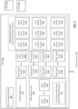
- FIG. 3 is a block diagram illustrating a processor to generate and store PEBS and NPEBS records according to examples. Any or all of the blocks shown in FIG. 3 may represent circuitry and/or logic in a performance management unit (PMU) of the processor.
- PMU performance management unit
- the PMU supports timed PEBS and a hybrid enumeration architecture via CPUID.
- a CPUID leaf enhances enumeration of PMU capabilities.
- CPUID sub-leafing accommodates future PMU extensions, hybrid resources are exposed per core-type, a bitmap hybrid enumeration of general counters availability is used, a bitmap hybrid enumeration of fixed counters availability is used, and new architectural PMU capabilities can be exposed via CPUID.
- a core 302 of a multicore processor (e.g., having one or more performance core(s) and one or more efficiency core(s) - other cores 390 and 393 are shown and they may be either performance or efficiency) includes an NPEBS handler circuit 306 and a PEBS handler circuit 308 (e.g., performance monitor 180) having one or more memory storages 330a to 330n (which may be implemented as physical memory storage such as a buffer).
- the PEBS handler circuit 308 may also include a performance monitoring interrupt (PMI) component 332 as described above.
- PMI performance monitoring interrupt
- the processor core 302 may include one or more event select (ES) controls 334a to 334n corresponding to one or more general purpose performance counters 336a - 336n and further corresponding to one or more PEBS enable circuits 338a - 338n (details of which are described above).
- PEBS enable circuits 338a- 338n may be located in a single control register (e.g., machine specific register or MSR).
- MSR machine specific register
- the performance core(s) and efficiency core(s) share an instruction set architecture.
- the performance core(s) and efficiency core(s) have different instruction set architectures.
- PEBS, NPEBS, and Precise Distribution of Instructions Retired (PDIR) operations are applied using fixed function counters 360a-360c.
- the three fixed function counters 360a-360c are defined and implemented to count instructions retired, reference clocks, and core clocks. It will be appreciated, however, that the underlying principles of the invention are not limited to any particular number of fixed function counters or any particular fixed function counter implementation.
- the processor core 302 may execute a stream of instructions that may be embedded with markers for events that may be placed on a bus/interconnect fabric 304.
- the execution of a segment of instructions may constitute one or more non-precise events.
- a non-precise event is a performance event that is either not linked to a specific instruction or micro-operation in an instruction trace or can occur speculatively when the instruction or micro-operation does not retire.
- Such non-precise events may include, but are not limited to, reference clocks, core clocks and cycles, to name a few examples.
- the non-precise event is generated by the processor core 302.
- the non-precise event is generated outside the processor core 302 and communicated to the processor via the bus/interconnect fabric 304.
- event select (ES) controls 350a-c shown in FIG. 3 perform similar operations to ES controls 334a-c described above but correspond to the fixed function performance counters 360a-c and further correspond to PEBS enable circuits 370a-c associated with the fixed function counters 360a-c.
- the PEBS enable circuits 338a- 338n and 370a-c are located in a single control register.
- the programming of the ES controls 350a-c causes a performance counter 360a-c corresponding to the programmed ES control to track occurrences of the particular programmed non-precise/precise event. In some examples, any event that is not defined as a precise event is considered a non-precise event.
- the ES control 350a-c is programmed by an executing application. In another example, a user programs the ES control 350a-c with the non-precise/precise event identifier.
- the performance counter 360a-c corresponding to the ES control 350a-c is incremented or decremented upon each occurrence of the programmed event.
- the PEBS enable circuit 370a-c corresponding to the ES control 350a-c and the fixed function performance counter 360a-c may be set (e.g., activated, flag set, bit set to 3, etc.) to generate a PEBS record upon overflow of the fixed function performance counter 360a-c or, if the counter is decremented, upon the fixed function performance counter 360a-c reaching a value of 0.
- PEBS enable bits are set to enable the PEBS handler circuit 308 to generate a PEBS record upon overflow or zero value of the fixed function performance counter 360a-c that is counting the event.
- a PEBS record includes an architectural metadata of a state of the system upon the overflow or zero value of the fixed function performance counter 360a-c.
- the architectural metadata may include, but is not limited to, an IP, TSC, or register state, for example.
- the NPEBS handler circuit 306 is coupled to the PEBS enable circuit 370a-c such that when the fixed function performance counter 360a-c overflows or reaches a zero value, the NPEBS handler circuit 306 causes the PEBS enable circuit 370a-c to generate the PEBS record for the event.
- the NPEBS handler circuit 306 controls timing of generation of the PEBS record for the event. For example, in one example, the NPEBS handler circuit 306 causes the PEBS enable circuit 370a-c to generate the PEBS record for the event immediately upon occurrence of the overflow or zero value of the performance counter 360a-c, tracking and counting the programmed event.
- the NPEBS handler circuit 306 causes the PEBS enable circuit 370a-c to generate the PEBS record for the event immediately after the occurrence of the overflow or zero value of the fixed function performance counter 360a-c, tracking and counting the programmed event.
- the PEBS record is generated after the next instruction that retires (i.e., after completion of the next instruction in the instruction trace that triggered the fixed function performance counter 360a-c to overflow or run to zero).
- the PEBS record generated for the event by PEBS handler circuit 308 is stored in memory storage 330 of the PEBS handler circuit 308. Accordingly, the architectural metadata associated with the event may be captured without utilizing a PMI.
- the PMI component 332 collects the PEBS records stored in the memory storage(s) 330a- 330n of PEBS handler circuit 308.
- the PMI component 332 may immediately collect the PEBS records stored in the memory storage 330a- 330n.
- the PMI component 332 is delayed in collecting the PEBS records in memory storage 330a-330n at once.
- the interface may be provided as an MSR.
- a performance capabilities control register 380 (e.g., PERF_CAPABILITIES MSR) enhances enumeration for PMU non-architectural features.
- this register 380 includes a per-field attributed to indicated whether the reporting is common or hybrid across core-types.
- An example format is as follows. Field Name Bits 1 Type LBR FMT 5:0 Common PEBS Trap 6 Common PEBS Arch Regs 7 Common PEBS FMT 11:8 Common Freeze while SMM 12 Common Full Write 13 Common PEBS Baseline 14 Common Perf Metrics Available 15 Hybrid PEBS Output PT Available 16 Hybrid PEBS Timing Info 17 Common TSX Store Address Register 18 Hybrid RDPMC Clear Metrics 19 Hybrid
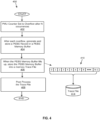
- FIG. 4 illustrates an example of operations 400 of a process to generate and store PEBS records in a memory buffer, and to store the memory buffer to a PEBS trace file.
- a PMU counter is set to -N. Starting at a negative value, the PMU counter in this example is to be incremented every time a PEBS record is generated, until it reaches zero (0). In an alternate example, not shown, the PMU counter is set to +N, and decremented every time a PEBS record is generated.
- N number of PEBS records are generated and stored in a PEBS memory buffer.
- the N PEBS records 410 are stored in a PEBS trace file 414. This step is also illustrated as 230, showing N PEBS records being stored in a PEBS trace file 414.
- the PEBS trace file is post-processed, after which the process ends.
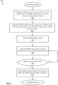
- FIG. 5 illustrates an example of operations 500 of a process of programming a PEBS handler circuit to monitor processor performance and generate a PEBS record to be stored in a PEBS memory buffer, and then stored in a PEBS trace file.
- a PMU counter is programmed to count function calls, such as BR_INST_RETIRED and NEAR_CALL_PS event, and to overflow after N calls.
- the PEBS handler circuit is programmed to generate, after each overflow, a PEBS record configured to contain architectural metadata including state information of the processor including, but not limited to, an instruction pointer, a time stamp counter, and register state, as well as performance cost. Configuration of the processor information monitored by PEBS and stored in a PEBS data record.
- a PEBS handler circuit is enabled.
- a PEBS record is generated upon counter overflow, and stored in PEBS memory buffer.
- a check if the PEBS memory buffer is full is performed, and if no, return to block 508, and if yes, proceed to block 512.
- the PEBS memory e.g., buffer
- the PEBS memory contents are stored to a PEBS trace file. The process then ends.
- architectural performance monitoring a range for the counters' MSRs in the 19xxH address range.
- This MSR range allows for at least scaling the number of general-purpose and fixed-function counters beyond the quantities in current products. Additionally, it banks registers of the same counter closer to each other.
- the PMC_GPn_CTR MSR holds the counter value with full-width write support1.
- the MSR address is 1900H + 4 * n.
- the PMC_GP1_CTR MSR has MSR address 1904H.
- the aliased register for legacy counters is in MSR address 4C1H + n.
- the PMC_GPn_CFG_A MSR is the Performance Event Select Register at address 1901H + 4 * n.
- PMC_GP1_CFG_A has MSR address 1905H.
- the aliased register for legacy counters is in MSR address 186H + n.
- the PMC_FXm_CTR MSR holds the counter value.
- the MSR address is 1980H + 4* m.
- IXED_CTR1 has MSR address 1984H.
- the aliased register for legacy counters is in MSR address 309H + m.
- UMASK2 field (e.g., bits 40 through 47) qualify the condition that the selected event logic unit detects. Valid UMASK2 values for each event logic unit are specific to the unit. The new UMASK2 field may also be used in conjunction with UMASK.
- An example architectural performance monitoring layout of the PERFEVTSELx MSRs (e.g., Unit Mask 2 (UMASK2) field 608) is shown in FIG. 6 .
- Automatic counter reloader logic e.g., automatic counter reloader logic 190 or part of PEBS handler circuit 308 (circuitry, firmware, a combination thereof, etc.) provides a means for Auto Counter Reload (ACR) for software to specify that, for each supported counter, the performance monitor hardware should automatically reload the counter to a specified initial value upon overflow of chosen counters.
- ACR Auto Counter Reload
- This mechanism enables software to sample based on the relative rate of two (or more) events, such that a sample (PMI or PEBS) is taken only if the rate of one event exceeds some threshold relative to the rate of another event. Common examples may include sampling only when IPC (instructions per cycle) drops below a threshold or MPKI (mispredicts per 1000 instructions) exceeds a threshold. In some examples, the threshold is user configurable.
- bit fields in PMCx_RELOAD_CFG may have the following meaning:
- the overflow bit (PERF_GLOBAL_STATUS.PMCx_OVF) will never be set. Instead, upon overflow, the counter will be immediately reloaded; thus, it is never in an overflowed state. There is an exception associated with PEBS.
- FIXED_CTRx For FIXED_CTRx, the reload value is stored in FIXED_CTRx_EXT[31:0], and which counters cause reload of FIXED _CTRx is configured in FIXED_CTRx_RELOAD_CFG.
- ACR reload is not guaranteed to be precise in some examples; in some cases, a small number of events may be lost during the time between counter overflow and counter reload.
- the overflow of a single counter is configured to reload multiple counters, it is guaranteed that those counters will be reloaded simultaneously.
- the counter reload actions will be taken only after the PEBS record has been written. This ensures that any counter values captured in the PEBS record reflect the value before the reload occurs. Because some latency is associated with PEBS record generation, this could result in more lost counts due to more time passing between counter overflow and counter reload.
- the overflow bit associated with the counter (in PERF_GLOBAL_STATUS) will be set from the time the counter overflows to the time the PEBS record is written. This is required to ensure the PEBS record is not lost due to a VM exit taken during record generation. Once the record is written, the overflow bit will be cleared, and the counter reloaded.
- Pdist When counters that support a precise distribution (PDIST) are reloaded by ACR, the PDIST behavior will be lost. With Pdist, the PEBS record will be generated precisely upon completion of the instruction or operation that causes the counter to overflow (there is no "wait for next occurrence" by default). Pdist is supported by selected counters, and is only supported when those counters are programmed to count select precise events.
- Certain architectural performance monitoring (PerfMon) facilities include a set of performance monitoring counters and performance event select registers.
- Certain examples herein add an "equal" (EQ) flag (e.g., as bit 36 of PERFEVTSELx MSRs), for example, such that when the EQ flag is set (e.g., to one) and an invert counter mask (INV) flag is clear (e.g., set to zero), a comparison of a threshold evaluates to true if the selected performance monitoring event is equal to the specified counter mask (Cmask) value.
- EQ equal
- IOV invert counter mask
- the comparison evaluates to true if the event is less than the Cmask value and the event is not zero. In certain examples, if the Cmask is zero, the EQ flag is ignored. In certain examples, the equal field is referred to as the zero behavior ("Z") field.
- certain examples herein add an additional (e.g., 8-bit) unit mask field (e.g., to bits 47:40 of PERFEVTSELx MSRs), aka "UnitMask2". In certain examples, this is enumerated in new feature bit 0x21.0.EBX[0],
- the UMASK2 field e.g., bits 40 through 47 bits qualify the condition that the selected event logic unit detects. In certain examples, valid UMASK2 values for each event logic unit are specific to the unit.
- the second UMASK2 field may also be used in conjunction with a first UMASK field, e.g., as shown in FIG. 6 .
- IA32_PERFEVTSELx MSRs start at address 186H and occupy a contiguous block of MSR address space.
- each performance event select register is paired with a corresponding performance counter, e.g., in the 0C1H address block.
- the number of IA32_PERFEVTSELx MSRs may vary from the number of physical counters present on the hardware, e.g., because an agent running at a higher privilege level (e.g., a virtual machine monitor (VMM)) may not expose all counters.
- VMM virtual machine monitor
- the bit width of an IA32_PMCx MSR is reported using the CPUID.0H:EAX[23:16], e.g., the number of valid bits for a read operation.
- the lower-order 32 bits of the MSR may be written with any value, and the high-order bits are sign-extended from the value of bit 31.
- the bit field layout of IA32_PERFEVTSELx MSRs is defined architecturally.
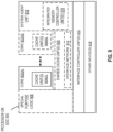
- FIG. 6 illustrates examples of architectural performance monitoring layouts of the PERFEVTSELx MSRs 600.
- PERFEVTSELx MSRs 600 is 64 bits wide (e.g., as shown) or 32 bits wide.
- control register 185 in FIG. 1 and/or control register 380 in FIG. 3 utilizes the format of MSR 600.
- PERFEVTSELx MSRs 600 includes an event select field, e.g., bits 0-7 of PERFEVTSELx MSRs 600 (e.g., of bit indices 0 to 63).
- the event select field allows for the selection of event logic unit used to detect microarchitectural conditions.
- the set of values for this field is defined architecturally, e.g., each value corresponds to an event logic unit for use with an architectural performance event.
- the number of architectural events is queried using CPUID.0H:EAX.
- a processor may support only a subset of pre-defined values.
- PERFEVTSELx MSRs 600 includes a unit mask (UMASK) field, e.g., bits 8-15 of PERFEVTSELx MSRs 600 (e.g., of bit indices 0 to 63).
- UMASK unit mask
- the unit mask field bits qualify the condition that the selected event logic unit detects.
- valid UMASK values for each event logic unit are specific to the unit.
- its corresponding UMASK value defines a specific microarchitectural condition.
- a pre-defined microarchitectural condition associated with an architectural event may not be applicable to a given processor, e.g., the processor then reports only a subset of pre-defined architectural events.
- pre-defined architectural events are listed in the table below.
- support for pre-defined architectural events is enumerated using CPUID.0H:EBX.
- Table 1 Example UMask and Event Select Encodings for Pre-Defined Architectural Performance Events Bit Position CPUID.AH.EBX Event Name UMask Event Select 0 UnHalted Core Cycles 00H 3CH 1 Instruction Retired 00H C0H 2 UnHalted Reference Cycles 01H 3CH 3 LCC Reference 4FH 2EH 4 LLC Misses 41H 2EH 5 Branch Instruction Retired 00H C4H 6 Branch Misses Retired 00H C5H 7 Topdown Slots 01H A4H
- PERFEVTSELx MSRs 600 includes a user mode (USR) field (e.g., bit or flag), e.g., bit 16 of PERFEVTSELx MSRs 600 (e.g., of bit indices 0 to 63).
- USB user mode
- the user mode field specifies that the selected microarchitectural condition is counted when the processor (e.g., core or logical processor) is operating at privilege levels 1, 2, or 3. This flag can be used with the OS flag.
- PERFEVTSELx MSRs 600 includes an operating system mode (OS) field (e.g., bit or flag), e.g., bit 17 of PERFEVTSELx MSRs 600 (e.g., of bit indices 0 to 63).
- OS operating system mode
- the operating system mode field specifies that the selected microarchitectural condition is counted when the processor (e.g., core or logical processor) is operating at privilege level 0 (e.g., OS or kernel level). This flag can be used with the USR flag.
- PERFEVTSELx MSRs 600 includes an edge detect (E) field (e.g., bit or flag), e.g., bit 18 of PERFEVTSELx MSRs 600 (e.g., of bit indices 0 to 63).
- the edge detect field enables (when set) edge detection of the selected microarchitectural condition.
- the processor e.g., core or logical processor
- this mechanism does not permit back-to-back assertions to be distinguished.
- this mechanism allows software to measure not only the fraction of time spent in a particular state, but also the average length of time spent in such a state (for example, the time spent waiting for an interrupt to be serviced).
- PERFEVTSELx MSRs 600 includes a pin control (PC) field (e.g., bit or flag), e.g., bit 19 of PERFEVTSELx MSRs 600 (e.g., of bit indices 0 to 63).
- the pin control field bit is reserved (not writeable).
- the processor e.g., core or logical processor
- the processor toggles the PMi pins and increments the counter when performance-monitoring events occur (e.g., and when the pin control field bit is cleared)
- the processor e.g., core or logical processor
- the toggling of a pin is defined as assertion of the pin for a single bus clock followed by de-assertion.
- PERFEVTSELx MSRs 600 includes an (e.g., Advanced Programmable Interrupt Controller (ACIP)) interrupt enable (INT) field (e.g., bit or flag), e.g., bit 20 of PERFEVTSELx MSRs 600 (e.g., of bit indices 0 to 63).
- ACIP Advanced Programmable Interrupt Controller
- the (e.g., ACIP) interrupt enable field when set, causes the processor (e.g., core or logical processor) to generates an exception through its local interrupt controller (e.g., APIC) on counter overflow.
- APIC local interrupt controller
- PERFEVTSELx MSRs 600 includes an any thread (ANY) field (e.g., bit or flag), e.g., bit 21 of PERFEVTSELx MSRs 600 (e.g., of bit indices 0 to 63).
- the any thread field is used for any processor (e.g., processor core) comprising of two or more logical processors.
- processor core e.g., processor core
- counting the associated event conditions e.g., including matching the thread's current privilege level (CPL) with the OS/USR setting of IA32_PERFEVTSELx
- each fixed-function performance counter IA32_FIXED_CTRx (e.g., starting at MSR address 309H) is configured by a (e.g., 4-bit) control block in the IA32_PERF_FIXED_CTR_CTRL MSR.
- the control block also allows thread specificity configuration using an Any Thread bit for fixed-function counters 0, 1, and 2.
- PERFEVTSELx MSRs 600 includes an enable counters (EN) field (e.g., bit or flag), e.g., bit 22 of PERFEVTSELx MSRs 600 (e.g., of bit indices 0 to 63).
- EN enable counters
- the enable counters field when set, enables performance counting in the corresponding performance-monitoring counter, e.g., and when clear, the corresponding counter is disabled.
- PERFEVTSELx MSRs 600 includes an invert counter mask (INV) field (e.g., bit or flag) 604, e.g., bit 23 of PERFEVTSELx MSRs 600 (e.g., of bit indices 0 to 63).
- the invert field 604 when set, inverts the counter-mask (CMASK) comparison, so that both greater than or equal to and less than comparisons can be made (e.g., set to a zero if greater than or equal, and set to 1 if less than).
- the counter mask (CMASK) is programmed to zero, INV flag is ignored.
- the INV field is used as discussed in reference to the logic table 700 in FIG. 7 .
- PERFEVTSELx MSRs 600 includes a counter mask (CMASK) field (e.g., bits) 606, e.g., bits 24-31 of PERFEVTSELx MSRs 600 (e.g., of bit indices 0 to 63).
- the counter mask field 606 e.g., when this field is not zero, causes a processor (e.g., core or logical processor) to compare this mask (e.g., threshold indicated by the mask) to the events count of the detected microarchitectural condition, e.g., during a single cycle.
- the counter is incremented by one, e.g., otherwise the counter is not incremented.
- this mask allows for software to characterize microarchitectural conditions that can count multiple occurrences per cycle (for example, two or more instructions retired per clock; or bus queue occupations).
- the counter-mask field is 0, then the counter is incremented each cycle by the event count associated with multiple occurrences.
- the CMASK field is used as discussed in reference to the logic table 700 in FIG. 7 .
- PERFEVTSELx MSRs 600 includes an in transaction region (IN_TX) field (e.g., bit or flag), e.g., bit 32 of PERFEVTSELx MSRs 600 (e.g., of bit indices 0 to 63).
- the in transaction region field when set, causes a counter to only include counts that occurred inside a transactional region, regardless of whether that region was aborted or committed. In certain examples, this bit may only be set if the processor supports hardware lock elision (HLE) or restricted transaction memory (RTM).
- HLE hardware lock elision
- RTM restricted transaction memory
- PERFEVTSELx MSRs 600 includes an in transaction exclude abort (IN_ TXCP) field (e.g., bit or flag), e.g., bit 33 of PERFEVTSELx MSRs 600 (e.g., of bit indices 0 to 63).
- the in transaction exclude abort field when set, causes a counter to not include counts that occurred inside of an aborted transactional region. In certain examples, this bit may only be set if the processor supports HLE or RTM. In certain examples, this bit may only be set for IA32 _PERFEVTSEL2.
- PERFEVTSELx MSRs 600 includes an adaptive record (AR) field (e.g., bit or flag), e.g., bit 34 of PERFEVTSELx MSRs 600 (e.g., of bit indices 0 to 63).
- AR adaptive record
- the adaptive record field when set, causes generation of an adaptive PEBS record (e.g., when set, modifies the sample information included in the PEBS record based on the configuration of an (e.g., separate) MSR).
- PERFEVTSELx MSRs 600 includes an LBR event logging enable (LEL) field (e.g., bit or flag), e.g., bit 35 of PERFEVTSELx MSRs 600 (e.g., of bit indices 0 to 63).
- LEL LBR event logging enable
- the LBR event logging enable field when set, enables occurrences of the chosen event to be additionally logged in a new LBR field (e.g., IA32_LBR_INFO.PMCx_CNT field).
- this two-bit field represents the number of occurrences of the event since retirement of the operation that last recorded an LBR entry, saturating at a value of 3.
- PERFEVTSELx MSRs 600 includes an equal (EQ) field 602 (e.g., bit or flag), e.g., bit 36 of PERFEVTSELx MSRs 600 (e.g., of bit indices 0 to 63).
- EQ flag 602 when the EQ flag 602 is set (e.g., to one) (e.g., and an invert counter mask (INV) flag 604 is clear (e.g., set to zero)), a comparison of a threshold evaluates to true if the selected performance monitoring event is equal to the specified counter mask (CMask) 606 value.
- CMask specified counter mask
- the comparison evaluates to true if the event is less than the CMask 606 value and the event is not zero. In certain examples, if the CMask is zero, the EQ flag is ignored. In certain examples, the equal field is referred to as the zero behavior ("Z") field. In certain examples, the EQ field is used as discussed in reference to the logic table 700 in FIG. 7 .
- some events may run out of usable unit mask bits, e.g., cache events or retired branch type.
- combining unit masks e.g., UMASK and UMASK2 in FIG. 6
- L0_HIT and L1_HIT UMasks for MEM LOAD_RETIRED give total data cache (e.g., data-cache unit (DCU)) hits.
- PERFEVTSELx MSRs 600 includes a second unit mask (UMASK2) field 608, e.g., bits 40-47 of PERFEVTSELx MSRs 600 (e.g., of bit indices 0 to 63).
- second unit mask (UMASK2) field 608 (i) allows an indication of more/additional events and/or allow more events and/or (ii) allows for combining with the other UMASK in FIG. 6 to synthesize new events.
- the value "N" (e.g., threshold) stored in the counter mask (CMASK) field 606 causes a performance monitor (e.g., a counter for the monitored event) to increment (or decrement) a counter when greater than or equal to "N" number of those monitored events (e.g., any event discussed herein) occur, e.g., in the same cycle.
- a performance monitor e.g., a counter for the monitored event
- increment e.g., a counter for the monitored event
- setting (e.g., to one) the invert counter mask (INV) flag 604 instead causes the performance monitor (e.g., a counter for the monitored event) to increment (or decrement) a counter when less than "N" number of events occur, e.g., in the same cycle.
- the performance monitor e.g., a counter for the monitored event
- increment (or decrement) a counter when less than "N" number of events occur, e.g., in the same cycle.
- BW bandwidth
- PERFEVTSELx MSRs 600 includes an equal (EQ) field (e.g., bit or flag) 602, e.g., bit 36 of PERFEVTSELx MSRs 600 (e.g., of bit indices 0 to 63).
- EQ equal
- bit or flag bit 36 of PERFEVTSELx MSRs 600
- FIG. 7 illustrates an example of a logic table (e.g., truth table) 700 using certain fields of a PERFEVTSELx MSR (e.g., MSR 600 in FIG. 6 ).
- a logic table e.g., truth table
- incrementing is mentioned, but it should be understood that a counter may be decremented in other examples. In certain examples, the counter is incremented and/or decremented by a value of 1.
- logic table 700 e.g., truth table
- a first mode, third mode, fifth mode, and seventh mode is indicated by the EQ flag 602 being cleared (e.g., set to zero),
- the counter mask (CMASK) field 606 being cleared causes the EQ flag 602 and INV flag 604 to be ignored, e.g., causes the corresponding counter to be incremented (e.g., by performance monitor 180 in FIG. 1 ) for each occurrence "X" of the corresponding (e.g., selected) performance monitoring event.
- a second mode (e.g., as shown in the corresponding line of logic table 700) is indicated by the EQ flag 602 being cleared (e.g., set to zero), the invert counter mask (INV) flag 604 being cleared (e.g., set to zero), and the counter mask (CMASK) field 606 being set to a non-zero value "N" (e.g., an integer), such that the corresponding counter is incremented (e.g., by performance monitor 180 in FIG. 1 ) only if the corresponding (e.g., selected) performance monitoring event count (e.g., in a single cycle) is equal to or greater than the specified counter mask (CMask) 606 value.
- N e.g., an integer
- a fourth mode (e.g., as shown in the corresponding line of logic table 700) is indicated by the EQ flag 602 being cleared (e.g., set to zero), the invert counter mask (INV) flag 604 being set (e.g., to one), and the counter mask (CMASK) field 606 being set to a non-zero value "N" (e.g., an integer), such that the corresponding counter is incremented (e.g., by performance monitor 180 in FIG. 1 ) only if the corresponding (e.g., selected) performance monitoring event count (e.g., in a single cycle) (e.g., including zero) is less than the specified counter mask (CMask) 606 value.
- N e.g., an integer
- a sixth mode (e.g., as shown in the corresponding line of logic table 700) is indicated by the EQ flag 602 being set (e.g., to one), the invert counter mask (INV) flag 604 being cleared (e.g., set to zero), and the counter mask (CMASK) field 606 being set to a non-zero value "N" (e.g., an integer), such that the corresponding counter is incremented (e.g., by performance monitor 180 in FIG.
- N e.g., an integer
- CMask specified counter mask
- an eighth mode (e.g., as shown in the corresponding line of logic table 700) is indicated by the EQ flag 602 being set (e.g., to one), the invert counter mask (INV) flag 604 being set (e.g., to one), and the counter mask (CMASK) field 606 being set to a non-zero value "N" (e.g., an integer), such that the corresponding counter is incremented (e.g., by performance monitor 180 in FIG.
- N e.g., an integer
- CMask specified counter mask
- a Performance Counter (e.g., MSR to control a performance counter) has a counter mask (CMask) 606 field to express a threshold number of events in a cycle.
- the equal bit 602 e.g., EQ bit or z bit
- this functionality (e.g., shown in the corresponding line(s) of logic table 700) is enumerated in new feature bit 0x21.0.EBX[1].
- the use of the EQ bit allows for the expression of certain (e.g., common) patterns with one counter and the EQ bit enables sampling over constructs with multiple counters.
- Some examples utilize instruction formats described herein. Some instructions support an 8-bit immediate. Some instructions support a 32-bit immediate. Some examples are implemented in one or more computer architectures, cores, accelerators, etc. Some examples are generated or are IP cores. Some examples utilize emulation and/or translation.
- an apparatus e.g., a processor
- the threshold field is a counter mask field of the control register.
- the control register comprises a mode field, and the performance monitor control circuit is to increment the performance monitoring counter in response to the performance monitoring event being equal to, but not greater than, the threshold field in response to the mode field being set to a first mode.
- the mode field set to the first mode comprises an equal field of the control register set to a one and an invert field of the control register set to zero.
- the performance monitor control circuit in response to the mode field of the control register being set to a second mode, is to increment the performance monitoring counter in response to the performance monitoring event being greater than zero and less than (e.g., but not equal to) the threshold field.
- the mode field set to the second mode comprises an equal field of the control register set to a one and an invert field of the control register set to one.
- the control register comprises a first unit mask field in a first half of the control register and second unit mask field in a second half of the control register.
- a method in another set of examples, includes executing, by an execution circuit of a processor, one or more instructions; setting a threshold field of a control register of the processor; and incrementing, by a performance monitor control circuit of the processor, a performance monitoring counter in response to a performance monitoring event of the one or more instructions being equal to, but not greater than, the threshold field.
- the threshold field is a counter mask field of the control register.
- the method further comprises setting a mode field of the control register to a first mode, wherein the incrementing, by the performance monitor control circuit, in response to the performance monitoring event being equal to, but not greater than, the threshold field, is in response to the mode field being set to the first mode.
- the setting the mode field to the first mode comprises setting an equal field of the control register to a one, and an invert field of the control register to zero.
- the method further comprises: setting the mode field of the control register to a second mode; and incrementing, by the performance monitor control circuit in response to the mode field being set to the second mode, the performance monitoring counter in response to the performance monitoring event being greater than zero and less than the threshold field.
- the setting the mode field to the second mode comprises setting an equal field of the control register to a one and an invert field of the control register to one.
- the control register comprises a first unit mask field in a first half of the control register and second unit mask field in a second half of the control register.
- an apparatus e.g., a processor
- the threshold field is a counter mask field of the control register.
- the control register comprises a mode field, and the performance monitor control circuit is to increment the performance monitoring counter in response to the performance monitoring event being equal to, but not greater than, the threshold field in response to the mode field being set to a first mode.
- the mode field set to the first mode comprises an equal field of the control register set to a one and an invert field of the control register set to zero.
- the performance monitor control circuit in response to the mode field of the control register being set to a second mode, is to increment the performance monitoring counter in response to the performance monitoring event being greater than zero and less than (e.g., but not equal to) the threshold field.
- the mode field set to the second mode comprises an equal field of the control register set to a one and an invert field of the control register set to one.
- the control register comprises a first unit mask field in a first half of the control register and second unit mask field in a second half of the control register.
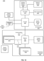
- FIG. 8 illustrates an example computing system.
- Multiprocessor system 800 is an interfaced system and includes a plurality of processors or cores including a first processor 870 and a second processor 880 coupled via an interface 850 such as a point-to-point (P-P) interconnect, a fabric, and/or bus.
- the first processor 870 and the second processor 880 are homogeneous.
- first processor 870 and the second processor 880 are heterogenous.
- the example system 800 is shown to have two processors, the system may have three or more processors, or may be a single processor system.
- the computing system is a system on a chip (SoC).
- SoC system on a chip
- Processors 870 and 880 are shown including integrated memory controller (IMC) circuitry 872 and 882, respectively.
- IMC integrated memory controller
- Processor 870 also includes interface circuits 876 and 878; similarly, second processor 880 includes interface circuits 886 and 888.
- Processors 870, 880 may exchange information via the interface 850 using interface circuits 878, 888.
- IMCs 872 and 882 couple the processors 870, 880 to respective memories, namely a memory 832 and a memory 834, which may be portions of main memory locally attached to the respective processors.
- Processors 870, 880 may each exchange information with a network interface (NW I/F) 890 via individual interfaces 852, 854 using interface circuits 876, 894, 886, 898.
- the network interface 890 e.g., one or more of an interconnect, bus, and/or fabric, and in some examples is a chipset
- the coprocessor 838 is a special-purpose processor, such as, for example, a high-throughput processor, a network or communication processor, compression engine, graphics processor, general purpose graphics processing unit (GPGPU), neural-network processing unit (NPU), embedded processor, or the like.
- a shared cache (not shown) may be included in either processor 870, 880 or outside of both processors, yet connected with the processors via an interface such as P-P interconnect, such that either or both processors' local cache information may be stored in the shared cache if a processor is placed into a low power mode.
- Network interface 890 may be coupled to a first interface 816 via interface circuit 896.
- first interface 816 may be an interface such as a Peripheral Component Interconnect (PCI) interconnect, a PCI Express interconnect or another I/O interconnect.
- PCI Peripheral Component Interconnect
- first interface 816 is coupled to a power control unit (PCU) 817, which may include circuitry, software, and/or firmware to perform power management operations with regard to the processors 870, 880 and/or co-processor 838.
- PCU 817 provides control information to a voltage regulator (not shown) to cause the voltage regulator to generate the appropriate regulated voltage.
- PCU 817 also provides control information to control the operating voltage generated.
- PCU 817 may include a variety of power management logic units (circuitry) to perform hardware-based power management.
- Such power management may be wholly processor controlled (e.g., by various processor hardware, and which may be triggered by workload and/or power, thermal or other processor constraints) and/or the power management may be performed responsive to external sources (such as a platform or power management source or system software).
- PCU 817 is illustrated as being present as logic separate from the processor 870 and/or processor 880. In other cases, PCU 817 may execute on a given one or more of cores (not shown) of processor 870 or 880. In some cases, PCU 817 may be implemented as a microcontroller (dedicated or general-purpose) or other control logic configured to execute its own dedicated power management code, sometimes referred to as P-code. In yet other examples, power management operations to be performed by PCU 817 may be implemented externally to a processor, such as by way of a separate power management integrated circuit (PMIC) or another component external to the processor. In yet other examples, power management operations to be performed by PCU 817 may be implemented within BIOS or other system software.
- PMIC power management integrated circuit
- Various I/O devices 814 may be coupled to first interface 816, along with a bus bridge 818 which couples first interface 816 to a second interface 820.
- one or more additional processor(s) 815 such as coprocessors, high throughput many integrated core (MIC) processors, GPGPUs, accelerators (such as graphics accelerators or digital signal processing (DSP) units), field programmable gate arrays (FPGAs), or any other processor, are coupled to first interface 816.
- second interface 820 may be a low pin count (LPC) interface.
- Various devices may be coupled to second interface 820 including, for example, a keyboard and/or mouse 822, communication devices 827 and storage circuitry 828.
- Storage circuitry 828 may be one or more non-transitory machine-readable storage media as described below, such as a disk drive or other mass storage device which may include instructions/code and data 830 and may implement the storage 828 in some examples. Further, an audio I/O 824 may be coupled to second interface 820. Note that other architectures than the point-to-point architecture described above are possible. For example, instead of the point-to-point architecture, a system such as multiprocessor system 800 may implement a multi-drop interface or other such architecture.
- Processor cores may be implemented in different ways, for different purposes, and in different processors.
- implementations of such cores may include: 1) a general purpose in-order core intended for general-purpose computing; 2) a high-performance general purpose out-of-order core intended for general-purpose computing; 3) a special purpose core intended primarily for graphics and/or scientific (throughput) computing.
- Implementations of different processors may include: 1) a CPU including one or more general purpose in-order cores intended for general-purpose computing and/or one or more general purpose out-of-order cores intended for general-purpose computing; and 2) a coprocessor including one or more special purpose cores intended primarily for graphics and/or scientific (throughput) computing.
- Such different processors lead to different computer system architectures, which may include: 1) the coprocessor on a separate chip from the CPU; 2) the coprocessor on a separate die in the same package as a CPU; 3) the coprocessor on the same die as a CPU (in which case, such a coprocessor is sometimes referred to as special purpose logic, such as integrated graphics and/or scientific (throughput) logic, or as special purpose cores); and 4) a system on a chip (SoC) that may be included on the same die as the described CPU (sometimes referred to as the application core(s) or application processor(s)), the above described coprocessor, and additional functionality.
- SoC system on a chip
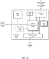
- FIG. 9 illustrates a block diagram of an example processor and/or SoC 900 that may have one or more cores and an integrated memory controller.
- the solid lined boxes illustrate a processor 900 with a single core 902(A), system agent unit circuitry 910, and a set of one or more interface controller unit(s) circuitry 916, while the optional addition of the dashed lined boxes illustrates an alternative processor 900 with multiple cores 902(A)-(N), a set of one or more integrated memory controller unit(s) circuitry 914 in the system agent unit circuitry 910, and special purpose logic 908, as well as a set of one or more interface controller units circuitry 916.
- the processor 900 may be one of the processors 870 or 880, or co-processor 838 or 815 of FIG. 8 .
- different implementations of the processor 900 may include: 1) a CPU with the special purpose logic 908 being integrated graphics and/or scientific (throughput) logic (which may include one or more cores, not shown), and the cores 902(A)-(N) being one or more general purpose cores (e.g., general purpose in-order cores, general purpose out-of-order cores, or a combination of the two); 2) a coprocessor with the cores 902(A)-(N) being a large number of special purpose cores intended primarily for graphics and/or scientific (throughput); and 3) a coprocessor with the cores 902(A)-(N) being a large number of general purpose in-order cores.
- the special purpose logic 908 being integrated graphics and/or scientific (throughput) logic
- the cores 902(A)-(N) being one or more general purpose cores (e.g., general purpose in-order cores, general purpose out-of-order cores, or a combination of the two)
- the processor 900 may be a general-purpose processor, coprocessor or special-purpose processor, such as, for example, a network or communication processor, compression engine, graphics processor, GPGPU (general purpose graphics processing unit), a high throughput many integrated core (MIC) coprocessor (including 30 or more cores), embedded processor, or the like.
- the processor may be implemented on one or more chips.
- the processor 900 may be a part of and/or may be implemented on one or more substrates using any of a number of process technologies, such as, for example, complementary metal oxide semiconductor (CMOS), bipolar CMOS (BiCMOS), P-type metal oxide semiconductor (PMOS), or N-type metal oxide semiconductor (NMOS).
- CMOS complementary metal oxide semiconductor
- BiCMOS bipolar CMOS
- PMOS P-type metal oxide semiconductor
- NMOS N-type metal oxide semiconductor
- a memory hierarchy includes one or more levels of cache unit(s) circuitry 904(A)-(N) within the cores 902(A)-(N), a set of one or more shared cache unit(s) circuitry 906, and external memory (not shown) coupled to the set of integrated memory controller unit(s) circuitry 914.
- the set of one or more shared cache unit(s) circuitry 906 may include one or more mid-level caches, such as level 2 (L2), level 3 (L3), level 4 (L4), or other levels of cache, such as a last level cache (LLC), and/or combinations thereof.
- LLC last level cache
- interface network circuitry 912 e.g., a ring interconnect
- special purpose logic 908 e.g., integrated graphics logic
- the set of shared cache unit(s) circuitry 906, and the system agent unit circuitry 910 alternative examples use any number of well-known techniques for interfacing such units.
- coherency is maintained between one or more of the shared cache unit(s) circuitry 906 and cores 902(A)-(N).
- interface controller units circuitry 916 couple the cores 902 to one or more other devices 918 such as one or more I/O devices, storage, one or more communication devices (e.g., wireless networking, wired networking, etc.), etc.
- the system agent unit circuitry 910 includes those components coordinating and operating cores 902(A)-(N).
- the system agent unit circuitry 910 may include, for example, power control unit (PCU) circuitry and/or display unit circuitry (not shown).
- the PCU may be or may include logic and components needed for regulating the power state of the cores 902(A)-(N) and/or the special purpose logic 908 (e.g., integrated graphics logic).
- the display unit circuitry is for driving one or more externally connected displays.
- the cores 902(A)-(N) may be homogenous in terms of instruction set architecture (ISA). Alternatively, the cores 902(A)-(N) may be heterogeneous in terms of ISA; that is, a subset of the cores 902(A)-(N) may be capable of executing an ISA, while other cores may be capable of executing only a subset of that ISA or another ISA.
- ISA instruction set architecture
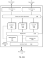
- FIG. 10 is a block diagram illustrating a computing system 1000 configured to implement one or more aspects of the examples described herein.
- the computing system 1000 includes a processing subsystem 1001 having one or more processor(s) 1002 and a system memory 1004 communicating via an interconnection path that may include a memory hub 1005.
- the memory hub 1005 may be a separate component within a chipset component or may be integrated within the one or more processor(s) 1002.
- the memory hub 1005 couples with an I/O subsystem 1011 via a communication link 1006.
- the I/O subsystem 1011 includes an I/O hub 1007 that can enable the computing system 1000 to receive input from one or more input device(s) 1008.
- the I/O hub 1007 can enable a display controller, which may be included in the one or more processor(s) 1002, to provide outputs to one or more display device(s) 1010A.
- the one or more display device(s) 1010A coupled with the I/O hub 1007 can include a local, internal, or embedded display device.
- the processing subsystem 100 includes one or more parallel processor(s) 1012 coupled to memory hub 1005 via a bus or other communication link 1013.
- the communication link 1013 may be one of any number of standards-based communication link technologies or protocols, such as, but not limited to PCI Express, or may be a vendor specific communications interface or communications fabric.
- the one or more parallel processor(s) 1012 may form a computationally focused parallel or vector processing system that can include a large number of processing cores and/or processing clusters, such as a many integrated core (MIC) processor.
- the one or more parallel processor(s) 1012 form a graphics processing subsystem that can output pixels to one of the one or more display device(s) 1010A coupled via the I/O hub 1007.
- the one or more parallel processor(s) 1012 can also include a display controller and display interface (not shown) to enable a direct connection to one or more display device(s) 1010B.
- a system storage unit 1014 can connect to the I/O hub 1007 to provide a storage mechanism for the computing system 1000.
- An I/O switch 1016 can be used to provide an interface mechanism to enable connections between the I/O hub 1007 and other components, such as a network adapter 1018 and/or wireless network adapter 1019 that may be integrated into the platform, and various other devices that can be added via one or more add-in device(s) 1020.
- the add-in device(s) 1020 may also include, for example, one or more external graphics processor devices, graphics cards, and/or compute accelerators.
- the network adapter 1018 can be an Ethernet adapter or another wired network adapter.
- the wireless network adapter 1019 can include one or more of a Wi-Fi, Bluetooth, near field communication (NFC), or other network device that includes one or more wireless radios.
- the computing system 1000 can include other components not explicitly shown, including USB or other port connections, optical storage drives, video capture devices, and the like, which may also be connected to the I/O hub 1007.
- Communication paths interconnecting the various components in FIG. 10 may be implemented using any suitable protocols, such as PCI (Peripheral Component Interconnect) based protocols (e.g., PCI-Express), or any other bus or point-to-point communication interfaces and/or protocol(s), such as the NVLink high-speed interconnect, Compute Express Link TM (CXL TM ) (e.g., CXL.mem), Infinity Fabric (IF), Ethernet (IEEE 802.3), remote direct memory access (RDMA), InfiniBand, Internet Wide Area RDMA Protocol (iWARP), Transmission Control Protocol (TCP), User Datagram Protocol (UDP), quick UDP Internet Connections (QUIC), RDMA over Converged Ethernet (RoCE), Intel QuickPath Interconnect (QPI), Intel Ultra Path Interconnect (UPI), Intel On-
- the one or more parallel processor(s) 1012 may incorporate circuitry optimized for graphics and video processing, including, for example, video output circuitry, and constitutes a graphics processing unit (GPU). Alternatively or additionally, the one or more parallel processor(s) 1012 can incorporate circuitry optimized for general purpose processing, while preserving the underlying computational architecture, described in greater detail herein.
- Components of the computing system 1000 may be integrated with one or more other system elements on a single integrated circuit.
- the one or more parallel processor(s) 1012, memory hub 1005, processor(s) 1002, and I/O hub 1007 can be integrated into a system on chip (SoC) integrated circuit.
- SoC system on chip
- the components of the computing system 1000 can be integrated into a single package to form a system in package (SIP) configuration.
- SIP system in package
- at least a portion of the components of the computing system 1000 can be integrated into a multi-chip module (MCM), which can be interconnected with other multi-chip modules into a modular computing system.
- connection topology including the number and arrangement of bridges, the number of processor(s) 1002, and the number of parallel processor(s) 1012, may be modified as desired.
- system memory 1004 can be connected to the processor(s) 1002 directly rather than through a bridge, while other devices communicate with system memory 1004 via the memory hub 1005 and the processor(s) 1002.
- the parallel processor(s) 1012 are connected to the I/O hub 1007 or directly to one of the one or more processor(s) 1002, rather than to the memory hub 1005.
- the I/O hub 1007 and memory hub 1005 may be integrated into a single chip. It is also possible that two or more sets of processor(s) 1002 are attached via multiple sockets, which can couple with two or more instances of the parallel processor(s) 1012.
- the memory hub 1005 may be referred to as a Northbridge in some architectures, while the I/O hub 1007 may be referred to as a Southbridge.
- FIG. 11A illustrates examples of a parallel processor 1100.
- the parallel processor 1100 may be a GPU, GPGPU or the like as described herein.
- the various components of the parallel processor 1100 may be implemented using one or more integrated circuit devices, such as programmable processors, application specific integrated circuits (ASICs), or field programmable gate arrays (FPGA).
- the illustrated parallel processor 1100 may be one or more of the parallel processor(s) 1012 shown in FIG. 10 .
- the parallel processor 1100 includes a parallel processing unit 1102.
- the parallel processing unit includes an I/O unit 1104 that enables communication with other devices, including other instances of the parallel processing unit 1102.
- the I/O unit 1104 may be directly connected to other devices.
- the I/O unit 1104 connects with other devices via the use of a hub or switch interface, such as memory hub 1005.
- the connections between the memory hub 1005 and the I/O unit 1104 form a communication link 1013.
- the I/O unit 1104 connects with a host interface 1106 and a memory crossbar 1116, where the host interface 1106 receives commands directed to performing processing operations and the memory crossbar 1116 receives commands directed to performing memory operations.
- the host interface 1106 can direct work operations to perform those commands to a front end 1108.
- the front end 1108 couples with a scheduler 1110, which is configured to distribute commands or other work items to a processing cluster array 1112.
- the scheduler 1110 ensures that the processing cluster array 1112 is properly configured and in a valid state before tasks are distributed to the processing clusters of the processing cluster array 1112.
- the scheduler 1110 may be implemented via firmware logic executing on a microcontroller.
- the microcontroller implemented scheduler 1110 is configurable to perform complex scheduling and work distribution operations at coarse and fine granularity, enabling rapid preemption and context switching of threads executing on the processing cluster array 1112.
- the host software can prove workloads for scheduling on the processing cluster array 1112 via one of multiple graphics processing doorbells.
- polling for new workloads or interrupts can be used to identify or indicate availability of work to perform.
- the workloads can then be automatically distributed across the processing cluster array 1112 by the scheduler 1110 logic within the scheduler microcontroller.
- the processing cluster array 1112 can include up to "N" processing clusters (e.g., cluster 1114A, cluster 1114B, through cluster 1114N). Each cluster 1114A-1114N of the processing cluster array 1112 can execute a large number of concurrent threads.
- the scheduler 1110 can allocate work to the clusters 1114A-1114N of the processing cluster array 1112 using various scheduling and/or work distribution algorithms, which may vary depending on the workload arising for each type of program or computation.
- the scheduling can be handled dynamically by the scheduler 1110 or can be assisted in part by compiler logic during compilation of program logic configured for execution by the processing cluster array 1112.
- different clusters 1114A-1114N of the processing cluster array 1112 can be allocated for processing different types of programs or for performing different types of computations.
- the processing cluster array 1112 can be configured to perform various types of parallel processing operations.
- the processing cluster array 1112 is configured to perform general-purpose parallel compute operations.
- the processing cluster array 1112 can include logic to execute processing tasks including filtering of video and/or audio data, performing modeling operations, including physics operations, and performing data transformations.
- the processing cluster array 1112 is configured to perform parallel graphics processing operations.
- the processing cluster array 1112 can include additional logic to support the execution of such graphics processing operations, including, but not limited to texture sampling logic to perform texture operations, as well as tessellation logic and other vertex processing logic.
- the processing cluster array 1112 can be configured to execute graphics processing related shader programs such as, but not limited to vertex shaders, tessellation shaders, geometry shaders, and pixel shaders.
- the parallel processing unit 1102 can transfer data from system memory via the I/O unit 1104 for processing. The transferred data can be stored to on-chip memory (e.g., parallel processor memory 1122) during processing, then written back to system memory.
- the scheduler 1110 may be configured to divide the processing workload into approximately equal sized tasks, to better enable distribution of the graphics processing operations to multiple clusters 1114A-1114N of the processing cluster array 1112.
- portions of the processing cluster array 1112 can be configured to perform different types of processing. For example, a first portion may be configured to perform vertex shading and topology generation, a second portion may be configured to perform tessellation and geometry shading, and a third portion may be configured to perform pixel shading or other screen space operations, to produce a rendered image for display.
- Intermediate data produced by one or more of the clusters 1114A-1114N may be stored in buffers to allow the intermediate data to be transmitted between clusters 1114A-1114N for further processing.
- the processing cluster array 1112 can receive processing tasks to be executed via the scheduler 1110, which receives commands defining processing tasks from front end 1108.
- processing tasks can include indices of data to be processed, e.g., surface (patch) data, primitive data, vertex data, and/or pixel data, as well as state parameters and commands defining how the data is to be processed (e.g., what program is to be executed).
- the scheduler 1110 may be configured to fetch the indices corresponding to the tasks or may receive the indices from the front end 1108.
- the front end 1108 can be configured to ensure the processing cluster array 1112 is configured to a valid state before the workload specified by incoming command buffers (e.g., batch-buffers, push buffers, etc.) is initiated.
- incoming command buffers e.g., batch-buffers, push buffers, etc.
- Each of the one or more instances of the parallel processing unit 1102 can couple with parallel processor memory 1122.
- the parallel processor memory 1122 can be accessed via the memory crossbar 1116, which can receive memory requests from the processing cluster array 1112 as well as the I/O unit 1104.
- the memory crossbar 1116 can access the parallel processor memory 1122 via a memory interface 1118.
- the memory interface 1118 can include multiple partition units (e.g., partition unit 1120A, partition unit 1120B, through partition unit 1120N) that can each couple to a portion (e.g., memory unit) of parallel processor memory 1122.
- the number of partition units 1120A-1120N may be configured to be equal to the number of memory units, such that a first partition unit 1120A has a corresponding first memory unit 1124A, a second partition unit 1120B has a corresponding second memory unit 1124B, and an Nth partition unit 1120N has a corresponding Nth memory unit 1124N. In other examples, the number of partition units 1120A-1120N may not be equal to the number of memory devices.
- the memory units 1124A-1124N can include various types of memory devices, including dynamic random-access memory (DRAM) or graphics random access memory, such as synchronous graphics random access memory (SGRAM), including graphics double data rate (GDDR) memory.
- DRAM dynamic random-access memory
- SGRAM synchronous graphics random access memory
- GDDR graphics double data rate
- the memory units 1124A-1124N may also include 3D stacked memory, including but not limited to high bandwidth memory (HBM).
- Render targets such as frame buffers or texture maps may be stored across the memory units 1124A-1124N, allowing partition units 1120A-1120N to write portions of each render target in parallel to efficiently use the available bandwidth of parallel processor memory 1122.
- a local instance of the parallel processor memory 1122 may be excluded in favor of a unified memory design that utilizes system memory in conjunction with local cache memory.
- any one of the clusters 1114A-1114N of the processing cluster array 1112 has the ability to process data that will be written to any of the memory units 1124A-1124N within parallel processor memory 1122.
- the memory crossbar 1116 can be configured to transfer the output of each cluster 1114A-1114N to any partition unit 1120A-1120N or to another cluster 1114A-1114N, which can perform additional processing operations on the output.
- Each cluster 1114A-1114N can communicate with the memory interface 1118 through the memory crossbar 1116 to read from or write to various external memory devices.
- the memory crossbar 1116 has a connection to the memory interface 1118 to communicate with the I/O unit 1104, as well as a connection to a local instance of the parallel processor memory 1122, enabling the processing units within the different processing clusters 1114A-1114N to communicate with system memory or other memory that is not local to the parallel processing unit 1102.
- the memory crossbar 1116 may, for example, be able to use virtual channels to separate traffic streams between the clusters 1114A-1114N and the partition units 1120A-1120N.
- the parallel processor 1100 can be an add-in device, such as add-in device 1020 of FIG. 10 , which may be a graphics card such as a discrete graphics card that includes one or more GPUs, one or more memory devices, and device-to-device or network or fabric interfaces.
- the different instances of the parallel processing unit 1102 can be configured to inter-operate even if the different instances have different numbers of processing cores, different amounts of local parallel processor memory, and/or other configuration differences.
- some instances of the parallel processing unit 1102 can include higher precision floating point units relative to other instances.
- Systems incorporating one or more instances of the parallel processing unit 1102 or the parallel processor 1100 can be implemented in a variety of configurations and form factors, including but not limited to desktop, laptop, or handheld personal computers, servers, workstations, game consoles, and/or embedded systems.
- An orchestrator can form composite nodes for workload performance using one or more of: disaggregated processor resources, cache resources, memory resources, storage resources, and networking resources.
- the parallel processing unit 1102 can be partitioned into multiple instances. Those multiple instances can be configured to execute workloads associated with different clients in an isolated manner, enabling a pre-determined quality of service to be provided for each client.
- each cluster 1114A-1114N can be compartmentalized and isolated from other clusters, allowing the processing cluster array 1112 to be divided into multiple compute partitions or instances. In such configuration, workloads that execute on an isolated partition are protected from faults or errors associated with a different workload that executes on a different partition.
- the partition units 1120A-1120N can be configured to enable a dedicated and/or isolated path to memory for the clusters 1114A-1114N associated with the respective compute partitions. This datapath isolation enables the compute resources within a partition can communicate with one or more assigned memory units 1124A-1124N without being subjected to inference by the activities of other partitions.
- FIG. 11B is a block diagram of a partition unit 1120.
- the partition unit 1120 may be an instance of one of the partition units 1120A-1120N of FIG. 11A .
- the partition unit 1120 includes an L2 cache 1121, a frame buffer interface 1125, and a ROP 1126 (raster operations unit).
- the L2 cache 1121 is a read/write cache that is configured to perform load and store operations received from the memory crossbar 1116 and ROP 1126. Read misses and urgent write-back requests are output by L2 cache 1121 to frame buffer interface 1125 for processing. Updates can also be sent to the frame buffer via the frame buffer interface 1125 for processing.
- the frame buffer interface 1125 interfaces with one of the memory units in parallel processor memory, such as the memory units 1124A-1124N of FIG. 11A (e.g., within parallel processor memory 1122).
- the partition unit 1120 may additionally or alternatively also interface with one of the memory units in parallel processor memory via a memory controller (not shown).
- the ROP 1126 is a processing unit that performs raster operations such as stencil, z test, blending, and the like.
- the ROP 1126 then outputs processed graphics data that is stored in graphics memory.
- the ROP 1126 includes or couples with a CODEC 1127 that includes compression logic to compress depth or color data that is written to memory or the L2 cache 1121 and decompress depth or color data that is read from memory or the L2 cache 1121.
- the compression logic can be lossless compression logic that makes use of one or more of multiple compression algorithms.
- the type of compression that is performed by the CODEC 1127 can vary based on the statistical characteristics of the data to be compressed. For example, in some examples, delta color compression is performed on depth and color data on a per-tile basis.
- the CODEC 1127 includes compression and decompression logic that can compress and decompress compute data associated with machine learning operations.
- the CODEC 1127 can, for example, compress sparse matrix data for sparse machine learning operations.
- the CODEC 1127 can also compress sparse matrix data that is encoded in a sparse matrix format (e.g., coordinate list encoding (COO), compressed sparse row (CSR), compress sparse column (CSC), etc.) to generate compressed and encoded sparse matrix data.
- the compressed and encoded sparse matrix data can be decompressed and/or decoded before being processed by processing elements or the processing elements can be configured to consume compressed, encoded, or compressed and encoded data for processing.
- the ROP 1126 may be included within each processing cluster (e.g., cluster 1114A-1114N of FIG. 11A ) instead of within the partition unit 1120. In such example, read and write requests for pixel data are transmitted over the memory crossbar 1116 instead of pixel fragment data.
- the processed graphics data may be displayed on a display device, such as one of the one or more display device(s) 1010A-1010B of FIG. 10 , routed for further processing by the processor(s) 1002, or routed for further processing by one of the processing entities within the parallel processor 1100 of FIG. 11A .
- FIG. 11C is a block diagram of a processing cluster 1114 within a parallel processing unit.
- the processing cluster is an instance of one of the processing clusters 1114A-1114N of FIG. 11A .
- the processing cluster 1114 can be configured to execute many threads in parallel, where the term "thread” refers to an instance of a particular program executing on a particular set of input data.
- SIMD single-instruction, multiple-data
- SIMT single-instruction, multiple-thread
- Operation of the processing cluster 1114 can be controlled via a pipeline manager 1132 that distributes processing tasks to SIMT parallel processors.
- the pipeline manager 1132 receives instructions from the scheduler 1110 of FIG. 11A and manages execution of those instructions via a graphics multiprocessor 1134 and/or a texture unit 1136.
- the illustrated graphics multiprocessor 1134 is an exemplary instance of a SIMT parallel processor. However, various types of SIMT parallel processors of differing architectures may be included within the processing cluster 1114.
- One or more instances of the graphics multiprocessor 1134 can be included within a processing cluster 1114.
- the graphics multiprocessor 1134 can process data and a data crossbar 1140 can be used to distribute the processed data to one of multiple possible destinations, including other shader units.
- the pipeline manager 1132 can facilitate the distribution of processed data by specifying destinations for processed data to be distributed via the data crossbar 1140.
- Each graphics multiprocessor 1134 within the processing cluster 1114 can include an identical set of functional execution logic (e.g., arithmetic logic units, load-store units, etc.).
- the functional execution logic can be configured in a pipelined manner in which new instructions can be issued before previous instructions are complete.
- the functional execution logic supports a variety of operations including integer and floating-point arithmetic, comparison operations, Boolean operations, bit-shifting, and computation of various algebraic functions.
- the same functional-unit hardware could be leveraged to perform different operations and any combination of functional units may be present.
- the instructions transmitted to the processing cluster 1114 constitute a thread.
- a set of threads executing across the set of parallel processing engines is a thread group.
- a thread group executes the same program on different input data.
- Each thread within a thread group can be assigned to a different processing engine within a graphics multiprocessor 1134.
- a thread group may include fewer threads than the number of processing engines within the graphics multiprocessor 1134. When a thread group includes fewer threads than the number of processing engines, one or more of the processing engines may be idle during cycles in which that thread group is being processed.
- a thread group may also include more threads than the number of processing engines within the graphics multiprocessor 1134. When the thread group includes more threads than the number of processing engines within the graphics multiprocessor 1134, processing can be performed over consecutive clock cycles.
- multiple thread groups can be executed concurrently on the graphics multiprocessor 1134.
- the graphics multiprocessor 1134 may include an internal cache memory to perform load and store operations.
- the graphics multiprocessor 1134 can forego an internal cache and use a cache memory (e.g., level 1 (L1) cache 1148) within the processing cluster 1114.
- Each graphics multiprocessor 1134 also has access to level 2 (L2) caches within the partition units (e.g., partition units 1120A-1120N of FIG. 11A ) that are shared among all processing clusters 1114 and may be used to transfer data between threads.
- L2 (L2) caches within the partition units (e.g., partition units 1120A-1120N of FIG. 11A ) that are shared among all processing clusters 1114 and may be used to transfer data between threads.
- the graphics multiprocessor 1134 may also access off-chip global memory, which can include one or more of local parallel processor memory and/or system memory. Any memory external to the parallel processing unit 1102 may be used as global memory. Examples in which the processing cluster 1114 includes multiple instances of the graphics multiprocessor 11
- Each processing cluster 1114 may include an MMU 1145 (memory management unit) that is configured to map virtual addresses into physical addresses.
- MMU 1145 memory management unit
- the MMU 1145 includes a set of page table entries (PTEs) used to map a virtual address to a physical address of a tile and optionally a cache line index.
- PTEs page table entries
- the MMU 1145 may include address translation lookaside buffers (TLB) or caches that may reside within the graphics multiprocessor 1134 or the L1 cache 1148 of processing cluster 1114.
- TLB address translation lookaside buffers
- the physical address is processed to distribute surface data access locality to allow efficient request interleaving among partition units.
- the cache line index may be used to determine whether a request for a cache line is a hit or miss.
- a processing cluster 1114 may be configured such that each graphics multiprocessor 1134 is coupled to a texture unit 1136 for performing texture mapping operations, e.g., determining texture sample positions, reading texture data, and filtering the texture data.
- Texture data is read from an internal texture L1 cache (not shown) or in some examples from the L1 cache within graphics multiprocessor 1134 and is fetched from an L2 cache, local parallel processor memory, or system memory, as needed.
- Each graphics multiprocessor 1134 outputs processed tasks to the data crossbar 1140 to provide the processed task to another processing cluster 1114 for further processing or to store the processed task in an L2 cache, local parallel processor memory, or system memory via the memory crossbar 1116.
- a preROP 1142 (pre-raster operations unit) is configured to receive data from graphics multiprocessor 1134, direct data to ROP units, which may be located with partition units as described herein (e.g., partition units 1120A-1120N of FIG. 11A ).
- the preROP 1142 unit can perform optimizations for color blending, organize pixel color data, and perform address translations.
- processing units e.g., graphics multiprocessor 1134, texture units 1136, preROPs 1142, etc.
- graphics multiprocessor 1134 may be included within a processing cluster 1114.
- texture units 1136 may be included within a processing cluster 1114.
- preROPs 1142 may be included within a processing cluster 1114.
- a parallel processing unit as described herein may include any number of instances of the processing cluster 1114.
- each processing cluster 1114 can be configured to operate independently of other processing clusters 1114 using separate and distinct processing units, L1 caches, L2 caches, etc.
- FIG. 11D shows an example of the graphics multiprocessor 1134 in which the graphics multiprocessor 1134 couples with the pipeline manager 1132 of the processing cluster 1114.
- the graphics multiprocessor 1134 has an execution pipeline including but not limited to an instruction cache 1152, an instruction unit 1154, an address mapping unit 1156, a register file 1158, one or more general purpose graphics processing unit (GPGPU) cores 1162, and one or more load/store units 1166.
- the GPGPU cores 1162 and load/store units 1166 are coupled with cache memory 1172 and shared memory 1170 via a memory and cache interconnect 1168.
- the graphics multiprocessor 1134 may additionally include tensor and/or ray-tracing cores 1163 that include hardware logic to accelerate matrix and/or ray-tracing operations.
- the instruction cache 1152 may receive a stream of instructions to execute from the pipeline manager 1132.
- the instructions are cached in the instruction cache 1152 and dispatched for execution by the instruction unit 1154.
- the instruction unit 1154 can dispatch instructions as thread groups (e.g., warps), with each thread of the thread group assigned to a different execution unit within GPGPU core 1162.
- An instruction can access any of a local, shared, or global address space by specifying an address within a unified address space.
- the address mapping unit 1156 can be used to translate addresses in the unified address space into a distinct memory address that can be accessed by the load/store units 1166.
- the register file 1158 provides a set of registers for the functional units of the graphics multiprocessor 1134.
- the register file 1158 provides temporary storage for operands connected to the data paths of the functional units (e.g., GPGPU cores 1162, load/store units 1166) of the graphics multiprocessor 1134.
- the register file 1158 may be divided between each of the functional units such that each functional unit is allocated a dedicated portion of the register file 1158. For example, the register file 1158 may be divided between the different warps being executed by the graphics multiprocessor 1134.
- the GPGPU cores 1162 can each include floating point units (FPUs) and/or integer arithmetic logic units (ALUs) that are used to execute instructions of the graphics multiprocessor 1134.
- the GPGPU cores 1162 can include hardware logic that may otherwise reside within the tensor and/or ray-tracing cores 1163.
- the GPGPU cores 1162 can be similar in architecture or can differ in architecture. For example and in some examples, a first portion of the GPGPU cores 1162 include a single precision FPU and an integer ALU while a second portion of the GPGPU cores include a double precision FPU.
- the FPUs can implement the IEEE 754-2008 standard for floating point arithmetic or enable variable precision floating point arithmetic.
- the graphics multiprocessor 1134 can additionally include one or more fixed function or special function units to perform specific functions such as copy rectangle or pixel blending operations.
- One or more of the GPGPU cores can also include fixed or special function logic.
- the GPGPU cores 1162 may include SIMD logic capable of performing a single instruction on multiple sets of data.
- GPGPU cores 1162 can physically execute SIMD4, SIMD8, and SIMD 16 instructions and logically execute SIMD1, SIMD2, and SIMD32 instructions.
- the SIMD instructions for the GPGPU cores can be generated at compile time by a shader compiler or automatically generated when executing programs written and compiled for single program multiple data (SPMD) or SIMT architectures. Multiple threads of a program configured for the SIMT execution model can be executed via a single SIMD instruction. For example and in some examples, eight SIMT threads that perform the same or similar operations can be executed in parallel via a single SIMD8 logic unit.
- the memory and cache interconnect 1168 is an interconnect network that connects each of the functional units of the graphics multiprocessor 1134 to the register file 1158 and to the shared memory 1170.
- the memory and cache interconnect 1168 is a crossbar interconnect that allows the load/store unit 1166 to implement load and store operations between the shared memory 1170 and the register file 1158.
- the register file 1158 can operate at the same frequency as the GPGPU cores 1162, thus data transfer between the GPGPU cores 1162 and the register file 1158 is very low latency.
- the shared memory 1170 can be used to enable communication between threads that execute on the functional units within the graphics multiprocessor 1134.
- the cache memory 1172 can be used as a data cache for example, to cache texture data communicated between the functional units and the texture unit 1136.
- the shared memory 1170 can also be used as a program managed cached.
- the shared memory 1170 and the cache memory 1172 can couple with the data crossbar 1140 to enable communication with other components of the processing cluster. Threads executing on the GPGPU cores 1162 can programmatically store data within the shared memory in addition to the automatically cached data that is stored within the cache memory 1172.
- FIGS. 12A-12C illustrate additional graphics multiprocessors, according to examples.
- FIG. 12A-12B illustrate graphics multiprocessors 1225, 1250, which are related to the graphics multiprocessor 1134 of FIG. 11C and may be used in place of one of those. Therefore, the disclosure of any features in combination with the graphics multiprocessor 1134 herein also discloses a corresponding combination with the graphics multiprocessor(s) 1225, 1250, but is not limited to such.
- FIG. 12C illustrates a graphics processing unit (GPU) 1280 which includes dedicated sets of graphics processing resources arranged into multi-core groups 1265A-1265N, which correspond to the graphics multiprocessors 1225, 1250.
- the illustrated graphics multiprocessors 1225, 1250 and the multi-core groups 1265A-1265N can be streaming multiprocessors (SM) capable of simultaneous execution of a large number of execution threads.
- SM streaming multiprocessors
- the graphics multiprocessor 1225 of FIG. 12A includes multiple additional instances of execution resource units relative to the graphics multiprocessor 1134 of FIG. 11D .
- the graphics multiprocessor 1225 can include multiple instances of the instruction unit 1232A-1232B, register file 1234A-1234B, and texture unit(s) 1244A-1244B.
- the graphics multiprocessor 1225 also includes multiple sets of graphics or compute execution units (e.g., GPGPU core 1236A-1236B, tensor core 1237A-1237B, ray-tracing core 1238A-1238B) and multiple sets of load/store units 1240A-1240B.
- the execution resource units have a common instruction cache 1230, texture and/or data cache memory 1242, and shared memory 1246.
- the various components can communicate via an interconnect fabric 1227.
- the interconnect fabric 1227 may include one or more crossbar switches to enable communication between the various components of the graphics multiprocessor 1225.
- the interconnect fabric 1227 may be a separate, high-speed network fabric layer upon which each component of the graphics multiprocessor 1225 is stacked.
- the components of the graphics multiprocessor 1225 communicate with remote components via the interconnect fabric 1227.
- the cores 1236A-1236B, 1237A-1237B, and 1238A-1238B can each communicate with shared memory 1246 via the interconnect fabric 1227.
- the interconnect fabric 1227 can arbitrate communication within the graphics multiprocessor 1225 to ensure a fair bandwidth allocation between components.
- the graphics multiprocessor 1250 of FIG. 12B includes multiple sets of execution resources 1256A-1256D, where each set of execution resource includes multiple instruction units, register files, GPGPU cores, and load store units, as illustrated in FIG. 11D and FIG. 12A .
- the execution resources 1256A-1256D can work in concert with texture unit(s) 1260A-1260D for texture operations, while sharing an instruction cache 1254, and shared memory 1253.
- the execution resources 1256A-1256D can share an instruction cache 1254 and shared memory 1253, as well as multiple instances of a texture and/or data cache memory 1258A-1258B.
- the various components can communicate via an interconnect fabric 1252 similar to the interconnect fabric 1227 of FIG. 12A .
- FIG. 1 , 11A-11D , and 12A-12B are descriptive and not limiting as to the scope of the present examples.
- the techniques described herein may be implemented on any properly configured processing unit, including, without limitation, one or more mobile application processors, one or more desktop or server central processing units (CPUs) including multi-core CPUs, one or more parallel processing units, such as the parallel processing unit 1102 of FIG. 11A , as well as one or more graphics processors or special purpose processing units, without departure from the scope of the examples described herein.
- CPUs desktop or server central processing units
- parallel processing units such as the parallel processing unit 1102 of FIG. 11A
- graphics processors or special purpose processing units without departure from the scope of the examples described herein.
- the parallel processor or GPGPU as described herein may be communicatively coupled to host/processor cores to accelerate graphics operations, machine-learning operations, pattern analysis operations, and various general-purpose GPU (GPGPU) functions.
- the GPU may be communicatively coupled to the host processor/cores over a bus or other interconnect (e.g., a high-speed interconnect such as PCIe, NVLink, or other known protocols, standardized protocols, or proprietary protocols).
- the GPU may be integrated on the same package or chip as the cores and communicatively coupled to the cores over an internal processor bus/interconnect (e.g., internal to the package or chip).
- the processor cores may allocate work to the GPU in the form of sequences of commands/instructions contained in a work descriptor.
- the GPU then uses dedicated circuitry/logic for efficiently processing these commands/instructions.
- FIG. 12C illustrates a graphics processing unit (GPU) 1280 which includes dedicated sets of graphics processing resources arranged into multi-core groups 1265A-1265N. While the details of only a single multi-core group 1265A are provided, it will be appreciated that the other multi-core groups 1265B-1265N may be equipped with the same or similar sets of graphics processing resources. Details described with respect to the multi-core groups 1265A-1265N may also apply to any graphics multiprocessor 1134, 1225, 1250 described herein.
- GPU graphics processing unit
- a multi-core group 1265A may include a set of graphics cores 1270, a set of tensor cores 1271, and a set of ray tracing cores 1272.
- a scheduler/dispatcher 1268 schedules and dispatches the graphics threads for execution on the various cores 1270, 1271, 1272.
- a set of register files 1269 store operand values used by the cores 1270, 1271, 1272 when executing the graphics threads. These may include, for example, integer registers for storing integer values, floating point registers for storing floating point values, vector registers for storing packed data elements (integer and/or floating-point data elements) and tile registers for storing tensor/matrix values.
- the tile registers may be implemented as combined sets of vector registers.
- I/O circuitry 1263 couples the GPU 1280 to one or more I/O devices 1262 such as digital signal processors (DSPs), network controllers, or user input devices.
- I/O devices 1262 such as digital signal processors (DSPs), network controllers, or user input devices.
- An on-chip interconnect may be used to couple the I/O devices 1262 to the GPU 1280 and memory 1266.
- IOMMUs I/O memory management units
- IOMMUs I/O memory management units
- the IOMMU 1264 manages multiple sets of page tables to map virtual addresses to physical addresses in system memory 1266.
- the I/O devices 1262, CPU(s) 1261, and GPU(s) 1280 may then share the same virtual address space.
- the IOMMU 1264 supports virtualization. In this case, it may manage a first set of page tables to map guest/graphics virtual addresses to guest/graphics physical addresses and a second set of page tables to map the guest/graphics physical addresses to system/host physical addresses (e.g., within system memory 1266).
- the base addresses of each of the first and second sets of page tables may be stored in control registers and swapped out on a context switch (e.g., so that the new context is provided with access to the relevant set of page tables). While not illustrated in FIG.
- the CPU(s) 1261, GPUs 1280, and I/O devices 1262 may be integrated on a single semiconductor chip and/or chip package.
- the illustrated memory 1266 may be integrated on the same chip or may be coupled to the memory controllers 1267 via an off-chip interface.
- the memory 1266 comprises GDDR6 memory which shares the same virtual address space as other physical system-level memories, although the underlying principles described herein are not limited to this specific implementation.
- the tensor cores 1271 may include a plurality of execution units specifically designed to perform matrix operations, which are the fundamental compute operation used to perform deep learning operations. For example, simultaneous matrix multiplication operations may be used for neural network training and inferencing.
- the tensor cores 1271 may perform matrix processing using a variety of operand precisions including single precision floating-point (e.g., 32 bits), half-precision floating point (e.g., 16 bits), integer words (16 bits), bytes (8 bits), and half-bytes (4 bits).
- a neural network implementation extracts features of each rendered scene, potentially combining details from multiple frames, to construct a high-quality final image.
- parallel matrix multiplication work may be scheduled for execution on the tensor cores 1271.
- the training of neural networks requires a significant number of matrix dot product operations.
- the tensor cores 1271 may include at least N dot-product processing elements. Before the matrix multiply begins, one entire matrix is loaded into tile registers and at least one column of a second matrix is loaded each cycle for N cycles. Each cycle, there are N dot products that are processed.
- Matrix elements may be stored at different precisions depending on the particular implementation, including 16-bit words, 8-bit bytes (e.g., INT8) and 4-bit half-bytes (e.g., INT4). Different precision modes may be specified for the tensor cores 1271 to ensure that the most efficient precision is used for different workloads (e.g., such as inferencing workloads which can tolerate quantization to bytes and half-bytes). Supported formats additionally include 64-bit floating point (FP64) and non-IEEE floating point formats such as the bfloat16 format (e.g., Brain floating point), a 16-bit floating point format with one sign bit, eight exponent bits, and eight significand bits, of which seven are explicitly stored.
- FP64 64-bit floating point
- non-IEEE floating point formats such as the bfloat16 format (e.g., Brain floating point), a 16-bit floating point format with one sign bit, eight exponent bits, and eight significand bits, of which seven are explicitly stored.
- One example includes support for a reduced precision tensor-float (TF32) mode, which performs computations using the range of FP32 (8-bits) and the precision of FP16 (10-bits). Reduced precision TF32 operations can be performed on FP32 inputs and produce FP32 outputs at higher performance relative to FP32 and increased precision relative to FP16. In some examples, one or more 8-bit floating point formats (FP8) are supported.
- TF32 reduced precision tensor-float
- FP8 8-bit floating point formats
- the tensor cores 1271 support a sparse mode of operation for matrices in which the vast majority of values are zero.
- the tensor cores 1271 include support for sparse input matrices that are encoded in a sparse matrix representation (e.g., coordinate list encoding (COO), compressed sparse row (CSR), compress sparse column (CSC), etc.).
- the tensor cores 1271 also include support for compressed sparse matrix representations in the event that the sparse matrix representation may be further compressed. Compressed, encoded, and/or compressed and encoded matrix data, along with associated compression and/or encoding metadata, can be read by the tensor cores 1271 and the non-zero values can be extracted.
- a non-zero value can be loaded from the compressed and/or encoded representation of at least a portion of matrix A. Based on the location in matrix A for the non-zero value, which may be determined from index or coordinate metadata associated with the non-zero value, a corresponding value in input matrix B may be loaded. Depending on the operation to be performed (e.g., multiply), the load of the value from input matrix B may be bypassed if the corresponding value is a zero value. In some examples, the pairings of values for certain operations, such as multiply operations, may be pre-scanned by scheduler logic and only operations between non-zero inputs are scheduled.
- output matrix C may be dense or sparse. Where output matrix C is sparse and depending on the configuration of the tensor cores 1271, output matrix C may be output in a compressed format, a sparse encoding, or a compressed sparse encoding.
- the ray tracing cores 1272 may accelerate ray tracing operations for both real-time ray tracing and non-real-time ray tracing implementations.
- the ray tracing cores 1272 may include ray traversal/intersection circuitry for performing ray traversal using bounding volume hierarchies (BVHs) and identifying intersections between rays and primitives enclosed within the BVH volumes.
- the ray tracing cores 1272 may also include circuitry for performing depth testing and culling (e.g., using a Z buffer or similar arrangement).
- the ray tracing cores 1272 perform traversal and intersection operations in concert with the image denoising techniques described herein, at least a portion of which may be executed on the tensor cores 1271.
- the tensor cores 1271 may implement a deep learning neural network to perform denoising of frames generated by the ray tracing cores 1272.
- the CPU(s) 1261, graphics cores 1270, and/or ray tracing cores 1272 may also implement all or a portion of the denoising and/or deep learning algorithms.
- a distributed approach to denoising may be employed in which the GPU 1280 is in a computing device coupled to other computing devices over a network or high-speed interconnect.
- the interconnected computing devices may share neural network learning/training data to improve the speed with which the overall system learns to perform denoising for different types of image frames and/or different graphics applications.
- the ray tracing cores 1272 may be adapted to accelerate general-purpose compute operations that can be accelerated using computational techniques that are analogous to ray intersection tests.
- a compute framework can be provided that enables shader programs to be compiled into low level instructions and/or primitives that perform general-purpose compute operations via the ray tracing cores.
- Exemplary computational problems that can benefit from compute operations performed on the ray tracing cores 1272 include computations involving beam, wave, ray, or particle propagation within a coordinate space. Interactions associated with that propagation can be computed relative to a geometry or mesh within the coordinate space. For example, computations associated with electromagnetic signal propagation through an environment can be accelerated via the use of instructions or primitives that are executed via the ray tracing cores. Diffraction and reflection of the signals by objects in the environment can be computed as direct ray-tracing analogies.
- Ray tracing cores 1272 can also be used to perform computations that are not directly analogous to ray tracing. For example, mesh projection, mesh refinement, and volume sampling computations can be accelerated using the ray tracing cores 1272. Generic coordinate space calculations, such as nearest neighbor calculations can also be performed. For example, the set of points near a given point can be discovered by defining a bounding box in the coordinate space around the point. BVH and ray probe logic within the ray tracing cores 1272 can then be used to determine the set of point intersections within the bounding box. The intersections constitute the origin point and the nearest neighbors to that origin point.
- Computations that are performed using the ray tracing cores 1272 can be performed in parallel with computations performed on the graphics cores 1272 and tensor cores 1271.
- a shader compiler can be configured to compile a compute shader or other general-purpose graphics processing program into low level primitives that can be parallelized across the graphics cores 1270, tensor cores 1271, and ray tracing cores 1272.
- Examples described herein provide techniques to disaggregate an architecture of a system on a chip integrated circuit into multiple distinct chiplets that can be packaged onto a common chassis.
- a graphics processing unit or parallel processor is composed from diverse silicon chiplets that are separately manufactured.
- a chiplet is an at least partially packaged integrated circuit that includes distinct units of logic that can be assembled with other chiplets into a larger package.
- a diverse set of chiplets with different IP core logic can be assembled into a single device.
- the chiplets can be integrated into a base die or base chiplet using active interposer technology.
- the concepts described herein enable the interconnection and communication between the different forms of IP within the GPU. The development of IPs on different process may be mixed. This avoids the complexity of converging multiple IPs, especially on a large SoC with several flavors IPs, to the same process.
- Enabling the use of multiple process technologies improves the time to market and provides a cost-effective way to create multiple product SKUs. For customers, this means getting products that are more tailored to their requirements in a cost effective and timely manner. Additionally, the disaggregated IPs are more amenable to being power gated independently, components that are not in use on a given workload can be powered off, reducing overall power consumption.
- FIG. 13 shows a parallel compute system 1300, according to some examples.
- the parallel compute system 1300 includes a parallel processor 1320, which can be a graphics processor or compute accelerator as described herein.
- the parallel processor 1320 includes a global logic unit 1301, an interface 1302, a thread dispatcher 1303, a media unit 1304, a set of compute units 1305A-1305H, and a cache/memory units 1306.
- the global logic unit 1301, in some examples, includes global functionality for the parallel processor 1320, including device configuration registers, global schedulers, power management logic, and the like.
- the interface 1302 can include a front-end interface for the parallel processor 1320.
- the thread dispatcher 1303 can receive workloads from the interface 1302 and dispatch threads for the workload to the compute units 1305A-1305H. If the workload includes any media operations, at least a portion of those operations can be performed by the media unit 1304. The media unit can also offload some operations to the compute units 1305A-1305H.
- the cache/memory units 1306 can include cache memory (e.g., L3 cache) and local memory (e.g., HBM, GDDR) for the parallel processor 1320.
- FIGS. 14A-14B illustrate a hybrid logical/physical view of a disaggregated parallel processor, according to examples described herein.
- FIG. 14A illustrates a disaggregated parallel compute system 1400.
- FIG. 14B illustrates a chiplet 1430 of the disaggregated parallel compute system 1400.
- a disaggregated compute system 1400 can include a parallel processor 1420 in which the various components of the parallel processor SOC are distributed across multiple chiplets.
- Each chiplet can be a distinct IP core that is independently designed and configured to communicate with other chiplets via one or more common interfaces.
- the chiplets include but are not limited to compute chiplets 1405, a media chiplet 1404, and memory chiplets 1406.
- Each chiplet can be separately manufactured using different process technologies. For example, compute chiplets 1405 may be manufactured using the smallest or most advanced process technology available at the time of fabrication, while memory chiplets 1406 or other chiplets (e.g., I/O, networking, etc.) may be manufactured using a larger or less advanced process technologies.
- the various chiplets can be bonded to a base die 1410 and configured to communicate with each other and logic within the base die 1410 via an interconnect layer 1412.
- the base die 1410 can include global logic 1401, which can include scheduler 1411 and power management 1421 logic units, an interface 1402, a dispatch unit 1403, and an interconnect fabric module 1408 coupled with or integrated with one or more L3 cache banks 1409A-1409N.
- the interconnect fabric 1408 can be an inter-chiplet fabric that is integrated into the base die 1410.
- Logic chiplets can use the fabric 1408 to relay messages between the various chiplets.
- L3 cache banks 1409A-1409N in the base die and/or L3 cache banks within the memory chiplets 1406 can cache data read from and transmitted to DRAM chiplets within the memory chiplets 1406 and to system memory of a host.
- the global logic 1401 is a microcontroller that can execute firmware to perform scheduler 1411 and power management 1421 functionality for the parallel processor 1420.
- the microcontroller that executes the global logic can be tailored for the target use case of the parallel processor 1420.
- the scheduler 1411 can perform global scheduling operations for the parallel processor 1420.
- the power management 1421 functionality can be used to enable or disable individual chiplets within the parallel processor when those chiplets are not in use.
- a set of compute chiplets 1405 can include clusters of compute units (e.g., execution units, streaming multiprocessors, etc.) that include programmable logic to execute compute or graphics shader instructions.
- a media chiplet 1404 can include hardware logic to accelerate media encode and decode operations.
- Memory chiplets 1406 can include volatile memory (e.g., DRAM) and one or more SRAM cache memory banks (e.g., L3 banks).
- each chiplet 1430 can include common components and application specific components.
- Chiplet logic 1436 within the chiplet 1430 can include the specific components of the chiplet, such as an array of streaming multiprocessors, compute units, or execution units described herein.
- the chiplet logic 1436 can couple with an optional cache or shared local memory 1438 or can include a cache or shared local memory within the chiplet logic 1436.
- the chiplet 1430 can include a fabric interconnect node 1442 that receives commands via the inter-chiplet fabric. Commands and data received via the fabric interconnect node 1442 can be stored temporarily within an interconnect buffer 1439. Data transmitted to and received from the fabric interconnect node 1442 can be stored in an interconnect cache 1440.
- Power control 1432 and clock control 1434 logic can also be included within the chiplet.
- the power control 1432 and clock control 1434 logic can receive configuration commands via the fabric can configure dynamic voltage and frequency scaling for the chiplet 1430.
- each chiplet can have an independent clock domain and power domain and can be clock gated and power gated independently of other chiplets.
- At least a portion of the components within the illustrated chiplet 1430 can also be included within logic embedded within the base die 1410 of FIG. 14A .
- logic within the base die that communicates with the fabric can include a version of the fabric interconnect node 1442.
- Base die logic that can be independently clock or power gated can include a version of the power control 1432 and/or clock control 1434 logic.
- SOC System on Chip
- a device or system can have one or more processors (e.g., one or more processor cores) and associated circuitry (e.g., Input/Output ("I/O") circuitry, power delivery circuitry, etc.) arranged in a disaggregated collection of discrete dies, tiles and/or chiplets (e.g., one or more discrete processor core die arranged adjacent to one or more other die such as memory die, I/O die, etc.).
- the various dies, tiles and/or chiplets can be physically and electrically coupled together by a package structure including, for example, various packaging substrates, interposers, active interposers, photonic interposers, interconnect bridges and the like.
- the disaggregated collection of discrete dies, tiles, and/or chiplets can also be part of a System-on-Package ("SoP").
- SoP System-on-Package
- FIG. 15A is a block diagram illustrating both an example in-order pipeline and an example register renaming, out-of-order issue/execution pipeline according to examples.
- FIG. 15B is a block diagram illustrating both an example in-order architecture core and an example register renaming, out-of-order issue/execution architecture core to be included in a processor according to examples.
- the solid lined boxes in FIGS. 15A-15B illustrate the in-order pipeline and in-order core, while the optional addition of the dashed lined boxes illustrates the register renaming, out-of-order issue/execution pipeline and core. Given that the in-order aspect is a subset of the out-of-order aspect, the out-of-order aspect will be described.
- a processor pipeline 1500 includes a fetch stage 1502, an optional length decoding stage 1504, a decode stage 1506, an optional allocation (Alloc) stage 1508, an optional renaming stage 1510, a schedule (also known as a dispatch or issue) stage 1512, an optional register read/memory read stage 1514, an execute stage 1516, a write back/memory write stage 1518, an optional exception handling stage 1522, and an optional commit stage 1524.
- One or more operations can be performed in each of these processor pipeline stages.
- one or more instructions are fetched from instruction memory, and during the decode stage 1506, the one or more fetched instructions may be decoded, addresses (e.g., load store unit (LSU) addresses) using forwarded register ports may be generated, and branch forwarding (e.g., immediate offset or a link register (LR)) may be performed.
- addresses e.g., load store unit (LSU) addresses
- branch forwarding e.g., immediate offset or a link register (LR)
- the decode stage 1506 and the register read/memory read stage 1514 may be combined into one pipeline stage.
- the decoded instructions may be executed, LSU address/data pipelining to an Advanced Microcontroller Bus (AMB) interface may be performed, multiply and add operations may be performed, arithmetic operations with branch results may be performed, etc.
- AMB Advanced Microcontroller Bus
- the example register renaming, out-of-order issue/execution architecture core of FIG. 15B may implement the pipeline 1500 as follows: 1) the instruction fetch circuitry 1538 performs the fetch and length decoding stages 1502 and 1504; 2) the decode circuitry 1540 performs the decode stage 1506; 3) the rename/allocator unit circuitry 1552 performs the allocation stage 1508 and renaming stage 1510; 4) the scheduler(s) circuitry 1556 performs the schedule stage 1512; 5) the physical register file(s) circuitry 1558 and the memory unit circuitry 1570 perform the register read/memory read stage 1514; the execution cluster(s) 1560 perform the execute stage 1516; 6) the memory unit circuitry 1570 and the physical register file(s) circuitry 1558 perform the write back/memory write stage 1518; 7) various circuitry may be involved in the exception handling stage 1522; and 8) the retirement unit circuitry 1554 and the physical register file(s) circuitry 1558 perform the commit stage 1524.
- FIG. 15B shows a processor core 1590 including front-end unit circuitry 1530 coupled to execution engine unit circuitry 1550, and both are coupled to memory unit circuitry 1570.
- the core 1590 may be a reduced instruction set architecture computing (RISC) core, a complex instruction set architecture computing (CISC) core, a very long instruction word (VLIW) core, or a hybrid or alternative core type.
- the core 1590 may be a special-purpose core, such as, for example, a network or communication core, compression engine, coprocessor core, general purpose computing graphics processing unit (GPGPU) core, graphics core, or the like.
- GPGPU general purpose computing graphics processing unit
- the front-end unit circuitry 1530 may include branch prediction circuitry 1532 coupled to instruction cache circuitry 1534, which is coupled to an instruction translation lookaside buffer (TLB) 1536, which is coupled to instruction fetch circuitry 1538, which is coupled to decode circuitry 1540.
- instruction cache circuitry 1534 is included in the memory unit circuitry 1570 rather than the front-end circuitry 1530.
- the decode circuitry 1540 (or decoder) may decode instructions, and generate as an output one or more micro-operations, microcode entry points, microinstructions, other instructions, or other control signals, which are decoded from, or which otherwise reflect, or are derived from, the original instructions.
- the decode circuitry 1540 may further include address generation unit (AGU, not shown) circuitry.
- AGU address generation unit
- the AGU generates an LSU address using forwarded register ports, and may further perform branch forwarding (e.g., immediate offset branch forwarding, LR register branch forwarding, etc.).
- the decode circuitry 1540 may be implemented using various different mechanisms. Examples of suitable mechanisms include, but are not limited to, look-up tables, hardware implementations, programmable logic arrays (PLAs), microcode read only memories (ROMs), etc.
- the core 1590 includes a microcode ROM (not shown) or other medium that stores microcode for certain macroinstructions (e.g., in decode circuitry 1540 or otherwise within the front-end circuitry 1530).
- the decode circuitry 1540 includes a micro-operation (micro-op) or operation cache (not shown) to hold/cache decoded operations, micro-tags, or micro-operations generated during the decode or other stages of the processor pipeline 1500.
- the decode circuitry 1540 may be coupled to rename/allocator unit circuitry 1552 in the execution engine circuitry 1550.
- the execution engine circuitry 1550 includes the rename/allocator unit circuitry 1552 coupled to retirement unit circuitry 1554 and a set of one or more scheduler(s) circuitry 1556.
- the scheduler(s) circuitry 1556 represents any number of different schedulers, including reservations stations, central instruction window, etc.
- the scheduler(s) circuitry 1556 can include arithmetic logic unit (ALU) scheduler/scheduling circuitry, ALU queues, address generation unit (AGU) scheduler/scheduling circuitry, AGU queues, etc.
- ALU arithmetic logic unit
- AGU address generation unit
- the scheduler(s) circuitry 1556 is coupled to the physical register file(s) circuitry 1558.
- Each of the physical register file(s) circuitry 1558 represents one or more physical register files, different ones of which store one or more different data types, such as scalar integer, scalar floating-point, packed integer, packed floating-point, vector integer, vector floating-point, status (e.g., an instruction pointer that is the address of the next instruction to be executed), etc.
- the physical register file(s) circuitry 1558 includes vector registers unit circuitry, writemask registers unit circuitry, and scalar register unit circuitry. These register units may provide architectural vector registers, vector mask registers, general-purpose registers, etc.
- the physical register file(s) circuitry 1558 is coupled to the retirement unit circuitry 1554 (also known as a retire queue or a retirement queue) to illustrate various ways in which register renaming and out-of-order execution may be implemented (e.g., using a reorder buffer(s) (ROB(s)) and a retirement register file(s); using a future file(s), a history buffer(s), and a retirement register file(s); using a register maps and a pool of registers; etc.).
- the retirement unit circuitry 1554 and the physical register file(s) circuitry 1558 are coupled to the execution cluster(s) 1560.
- the execution cluster(s) 1560 includes a set of one or more execution unit(s) circuitry 1562 and a set of one or more memory access circuitry 1564.
- the execution unit(s) circuitry 1562 may perform various arithmetic, logic, floating-point or other types of operations (e.g., shifts, addition, subtraction, multiplication) and on various types of data (e.g., scalar integer, scalar floating-point, packed integer, packed floating-point, vector integer, vector floating-point). While some examples may include a number of execution units or execution unit circuitry dedicated to specific functions or sets of functions, other examples may include only one execution unit circuitry or multiple execution units/execution unit circuitry that all perform all functions.
- the scheduler(s) circuitry 1556, physical register file(s) circuitry 1558, and execution cluster(s) 1560 are shown as being possibly plural because certain examples create separate pipelines for certain types of data/operations (e.g., a scalar integer pipeline, a scalar floating-point/packed integer/packed floating-point/vector integer/vector floating-point pipeline, and/or a memory access pipeline that each have their own scheduler circuitry, physical register file(s) circuitry, and/or execution cluster - and in the case of a separate memory access pipeline, certain examples are implemented in which only the execution cluster of this pipeline has the memory access unit(s) circuitry 1564). It should also be understood that where separate pipelines are used, one or more of these pipelines may be out-of-order issue/execution and the rest in-order.
- the execution engine unit circuitry 1550 may perform load store unit (LSU) address/data pipelining to an Advanced Microcontroller Bus (AMB) interface (not shown), and address phase and writeback, data phase load, store, and branches.
- LSU load store unit
- AMB Advanced Microcontroller Bus
- each instruction of an ISA is expressed using a given instruction format (and, if defined, in a given one of the instruction templates of that instruction format) and includes fields for specifying the operation and the operands.
- an example ADD instruction has a specific opcode and an instruction format that includes an opcode field to specify that opcode and operand fields to select operands (source1/destination and source2); and an occurrence of this ADD instruction in an instruction stream will have specific contents in the operand fields that select specific operands.
- FIG. 18 illustrates examples of an instruction format.
- an instruction may include multiple components including, but not limited to, one or more fields for: one or more prefixes 1801, an opcode 1803, addressing information 1805 (e.g., register identifiers, memory addressing information, etc.), a displacement value 1807, and/or an immediate value 1809.
- addressing information 1805 e.g., register identifiers, memory addressing information, etc.
- displacement value 1807 e.g., a displacement value 1807
- an immediate value 1809 e.g., a displacement value 1807
- the order illustrated is the order in which these fields are to be encoded, however, it should be appreciated that in other examples these fields may be encoded in a different order, combined, etc.
- the opcode field 1803 is used to at least partially define the operation to be performed upon a decoding of the instruction.
- a primary opcode encoded in the opcode field 1803 is one, two, or three bytes in length. In other examples, a primary opcode can be a different length.
- An additional 3-bit opcode field is sometimes encoded in another field.
- the addressing information field 1805 is used to address one or more operands of the instruction, such as a location in memory or one or more registers.
- FIG. 19 illustrates examples of the addressing information field 1805.
- an optional MOD R/M byte 1902 and an optional Scale, Index, Base (SIB) byte 1904 are shown.
- the MOD R/M byte 1902 and the SIB byte 1904 are used to encode up to two operands of an instruction, each of which is a direct register or effective memory address. Note that both of these fields are optional in that not all instructions include one or more of these fields.
- the MOD R/M byte 1902 includes a MOD field 1942, a register (reg) field 1944, and R/M field 1946.
- the content of the MOD field 1942 distinguishes between memory access and non-memory access modes. In some examples, when the MOD field 1942 has a binary value of 11 (1 1b), a register-direct addressing mode is utilized, and otherwise a register-indirect addressing mode is used.
- the register field 1944 may encode either the destination register operand or a source register operand or may encode an opcode extension and not be used to encode any instruction operand.
- the content of register field 1944 directly or through address generation, specifies the locations of a source or destination operand (either in a register or in memory).
- the register field 1944 is supplemented with an additional bit from a prefix (e.g., prefix 1801) to allow for greater addressing.
- the R/M field 1946 may be used to encode an instruction operand that references a memory address or may be used to encode either the destination register operand or a source register operand. Note the R/M field 1946 may be combined with the MOD field 1942 to dictate an addressing mode in some examples.
- the SIB byte 1904 includes a scale field 1952, an index field 1954, and a base field 1956 to be used in the generation of an address.
- the scale field 1952 indicates a scaling factor.
- the index field 1954 specifies an index register to use. In some examples, the index field 1954 is supplemented with an additional bit from a prefix (e.g., prefix 1801) to allow for greater addressing.
- the base field 1956 specifies a base register to use. In some examples, the base field 1956 is supplemented with an additional bit from a prefix (e.g., prefix 1801) to allow for greater addressing.
- the content of the scale field 1952 allows for the scaling of the content of the index field 1954 for memory address generation (e.g., for address generation that uses 2scale * index + base).
- addressing forms utilize a displacement value to generate a memory address.
- a memory address may be generated according to 2scale * index + base + displacement, index*scale + displacement, r/m + displacement, instruction pointer (RIP/EIP) + displacement, register + displacement, etc.
- the displacement may be a 1-byte, 2-byte, 4-byte, etc. value.
- the displacement field 1807 provides this value.
- a displacement factor usage is encoded in the MOD field of the addressing information field 1805 that indicates a compressed displacement scheme for which a displacement value is calculated and stored in the displacement field 1807.
- the immediate value field 1809 specifies an immediate value for the instruction.
- An immediate value may be encoded as a 1-byte value, a 2-byte value, a 4-byte value, etc.
- FIG. 20 illustrates examples of a first prefix 1801(A).
- the first prefix 1801(A) is an example of a REX prefix.
- Instructions that use this prefix may specify general purpose registers, 64-bit packed data registers (e.g., single instruction, multiple data (SIMD) registers or vector registers), and/or control registers and debug registers (e.g., CR8-CR15 and DR8-DR15).
- Instructions using the first prefix 1801(A) may specify up to three registers using 3-bit fields depending on the format: 1) using the reg field 1944 and the R/M field 1946 of the MOD R/M byte 1902; 2) using the MOD R/M byte 1902 with the SIB byte 1904 including using the reg field 1944 and the base field 1956 and index field 1954; or 3) using the register field of an opcode.
- bit positions of the payload byte 7:4 are set as 0100.
- bit position 2 (R) may be an extension of the MOD R/M reg field 1944 and may be used to modify the MOD R/M reg field 1944 when that field encodes a general-purpose register, a 64-bit packed data register (e.g., an SSE register), or a control or debug register. R is ignored when MOD R/M byte 1902 specifies other registers or defines an extended opcode.
- Bit position 0 (B) may modify the base in the MOD R/M R/M field 1946 or the SIB byte base field 1956; or it may modify the opcode register field used for accessing general purpose registers (e.g., general purpose registers 1725).
- FIGS. 21A-21D illustrate examples of how the R, X, and B fields of the first prefix 1801(A) are used.
- FIG. 21A illustrates R and B from the first prefix 1801(A) being used to extend the reg field 1944 and R/M field 1946 of the MOD R/M byte 1902 when the SIB byte 19 04 is not used for memory addressing.
- FIG. 21B illustrates R and B from the first prefix 1801(A) being used to extend the reg field 1944 and R/M field 1946 of the MOD R/M byte 1902 when the SIB byte 19 04 is not used (register-register addressing).
- FIG. 21A illustrates R and B from the first prefix 1801(A) being used to extend the reg field 1944 and R/M field 1946 of the MOD R/M byte 1902 when the SIB byte 19 04 is not used (register-register addressing).
- FIG. 21A illustrates R and B from the first prefix 1801(A) being used to extend the reg field 1944 and R/M field
- FIG. 21C illustrates R, X, and B from the first prefix 1801(A) being used to extend the reg field 1944 of the MOD R/M byte 1902 and the index field 1954 and base field 1956 when the SIB byte 19 04 being used for memory addressing.
- FIG. 21D illustrates B from the first prefix 1801(A) being used to extend the reg field 1944 of the MOD R/M byte 1902 when a register is encoded in the opcode 1803.
- FIGS. 22A-22B illustrate examples of a second prefix 1801(B).
- the second prefix 1801(B) is an example of a VEX prefix.
- the second prefix 1801(B) encoding allows instructions to have more than two operands, and allows SIMD vector registers (e.g., vector/SIMD registers 1710) to be longer than 64-bits (e.g., 128-bit and 256-bit).
- SIMD vector registers e.g., vector/SIMD registers 1710
- 64-bits e.g., 128-bit and 256-bit.
- the second prefix 1801(B) comes in two forms - a two-byte form and a three-byte form.
- the two-byte second prefix 1801(B) is used mainly for 128-bit, scalar, and some 256-bit instructions; while the three-byte second prefix 1801(B) provides a compact replacement of the first prefix 1801(A) and 3-byte opcode instructions.
- FIG. 22A illustrates examples of a two-byte form of the second prefix 1801(B).
- a format field 2201 (byte 0 2203) contains the value C5H.
- byte 1 2205 includes an "R" value in bit[7]. This value is the complement of the "R" value of the first prefix 1801(A).
- Bit[2] is used to dictate the length (L) of the vector (where a value of 0 is a scalar or 128-bit vector and a value of 1 is a 256-bit vector).
- Bits[6:3] shown as vvvv may be used to: 1) encode the first source register operand, specified in inverted (1s complement) form and valid for instructions with 2 or more source operands; 2) encode the destination register operand, specified in 1s complement form for certain vector shifts; or 3) not encode any operand, the field is reserved and should contain a certain value, such as 11 11b.
- Instructions that use this prefix may use the MOD R/M R/M field 1946 to encode the instruction operand that references a memory address or encode either the destination register operand or a source register operand.
- Instructions that use this prefix may use the MOD R/M reg field 1944 to encode either the destination register operand or a source register operand, or to be treated as an opcode extension and not used to encode any instruction operand.
- vvvv For instruction syntax that support four operands, vvvv, the MOD R/M R/M field 1946 and the MOD R/M reg field 1944 encode three of the four operands. Bits[7:4] of the immediate value field 1809 are then used to encode the third source register operand.
- FIG. 22B illustrates examples of a three-byte form of the second prefix 1801(B).
- a format field 2211 (byte 0 2213) contains the value C4H.
- Byte 1 2215 includes in bits[7:5] "R,” "X,” and "B” which are the complements of the same values of the first prefix 1801(A).
- Bits[4:0] of byte 1 2215 (shown as mmmmm) include content to encode, as need, one or more implied leading opcode bytes. For example, 00001 implies a 0FH leading opcode, 00010 implies a 0F38H leading opcode, 00011 implies a 0F3AH leading opcode, etc.
- Bit[7] of byte 2 2217 is used similar to W of the first prefix 1801(A) including helping to determine promotable operand sizes.
- Bit[2] is used to dictate the length (L) of the vector (where a value of 0 is a scalar or 128-bit vector and a value of 1 is a 256-bit vector).
- Instructions that use this prefix may use the MOD R/M R/M field 1946 to encode the instruction operand that references a memory address or encode either the destination register operand or a source register operand.
- Instructions that use this prefix may use the MOD R/M reg field 1944 to encode either the destination register operand or a source register operand, or to be treated as an opcode extension and not used to encode any instruction operand.
- vvvv For instruction syntax that support four operands, vvvv, the MOD R/M R/M field 1946, and the MOD R/M reg field 1944 encode three of the four operands. Bits[7:4] of the immediate value field 1809 are then used to encode the third source register operand.
- FIG. 23 illustrates examples of a third prefix 1801(C).
- the third prefix 1801(C) is an example of an EVEX prefix.
- the third prefix 1801(C) is a four-byte prefix.
- any set of elements in the destination when zeroing vector masks allow any set of elements in the destination to be zeroed during the execution of any operation (specified by the base operation and the augmentation operation); in some examples, an element of the destination is set to 0 when the corresponding mask bit has a 0 value.
- a subset of this functionality is the ability to control the vector length of the operation being performed (that is, the span of elements being modified, from the first to the last one); however, it is not necessary that the elements that are modified be consecutive.
- the opmask field allows for partial vector operations, including loads, stores, arithmetic, logical, etc.
- the execution units 2408A-2408N are primarily used to execute shader programs.
- a shader processor 2402 can process the various shader programs and dispatch execution threads associated with the shader programs via a thread dispatcher 2404.
- the thread dispatcher includes logic to arbitrate thread initiation requests from the graphics and media pipelines and instantiate the requested threads on one or more execution unit in the execution units 2408A-2408N.
- a geometry pipeline can dispatch vertex, tessellation, or geometry shaders to the thread execution logic for processing.
- thread dispatcher 2404 can also process runtime thread spawning requests from the executing shader programs.
- Each hardware thread within each execution unit has a dedicated high-bandwidth register file and associated independent thread-state. Execution is multi-issue per clock to pipelines capable of integer, single and double precision floating point operations, SIMD branch capability, logical operations, transcendental operations, and other miscellaneous operations.
- dependency logic within the execution units 2408A-2408N causes a waiting thread to sleep until the requested data has been returned. While the waiting thread is sleeping, hardware resources may be devoted to processing other threads. For example, during a delay associated with a vertex shader operation, an execution unit can perform operations for a pixel shader, fragment shader, or another type of shader program, including a different vertex shader.
- SIMT Single Instruction Multiple Thread
- Reference to a SIMD core or operation can apply also to SIMT or apply to SIMD in combination with SIMT.
- Each execution unit in execution units 2408A-2408N operates on arrays of data elements.
- the number of data elements is the "execution size," or the number of channels for the instruction.
- An execution channel is a logical unit of execution for data element access, masking, and flow control within instructions.
- the number of channels may be independent of the number of physical Arithmetic Logic Units (ALUs) or Floating Point Units (FPUs) for a particular graphics processor.
- ALUs Arithmetic Logic Units
- FPUs Floating Point Units
- execution units 2408A-2408N support integer and floating-point data types.
- the execution unit instruction set includes SIMD instructions.
- the various data elements can be stored as a packed data type in a register and the execution unit will process the various elements based on the data size of the elements. For example, when operating on a 256-bit wide vector, the 256 bits of the vector are stored in a register and the execution unit operates on the vector as four separate 64-bit packed data elements (Quad-Word (QW) size data elements), eight separate 32-bit packed data elements (Double Word (DW) size data elements), sixteen separate 16-bit packed data elements (Word (W) size data elements), or thirty-two separate 8-bit data elements (byte (B) size data elements).
- QW Quad-Word
- DW Double Word
- W 16-bit packed data elements
- B thirty-two separate 8-bit data elements
- one or more execution units can be combined into a fused execution unit 2409A-2409N having thread control logic (2407A-2407N) that is common to the fused EUs.
- Multiple EUs can be fused into an EU group.
- Each EU in the fused EU group can be configured to execute a separate SIMD hardware thread.
- the number of EUs in a fused EU group can vary according to examples. Additionally, various SIMD widths can be performed per-EU, including but not limited to SIMD8, SIMD16, and SIMD32.
- Each fused graphics execution unit 2409A-2409N includes at least two execution units.
- fused execution unit 2409A includes a first EU 2408A, second EU 2408B, and thread control logic 2407A that is common to the first EU 2408A and the second EU 2408B.
- the thread control logic 2407A controls threads executed on the fused graphics execution unit 2409A, allowing each EU within the fused execution units 2409A-2409N to execute using a common instruction pointer register.
- One or more internal instruction caches are included in the thread execution logic 2400 to cache thread instructions for the execution units.
- one or more data caches are included to cache thread data during thread execution. Threads executing on the execution logic 2400 can also store explicitly managed data in the shared local memory 2411.
- a sampler 2410 is included to provide texture sampling for 3D operations and media sampling for media operations.
- sampler 2410 includes specialized texture or media sampling functionality to process texture or media data during the sampling process before providing the sampled data to an execution unit.
- pixel processor logic within the shader processor 2402 is invoked to further compute output information and cause results to be written to output surfaces (e.g., color buffers, depth buffers, stencil buffers, etc.).
- output surfaces e.g., color buffers, depth buffers, stencil buffers, etc.
- a pixel shader or fragment shader calculates the values of the various vertex attributes that are to be interpolated across the rasterized object.
- pixel processor logic within the shader processor 2402 then executes an application programming interface (API)-supplied pixel or fragment shader program.
- API application programming interface
- the shader processor 2402 dispatches threads to an execution unit (e.g., 2408A) via thread dispatcher 2404.
- shader processor 2402 uses texture sampling logic in the sampler 2410 to access texture data in texture maps stored in memory. Arithmetic operations on the texture data and the input geometry data compute pixel color data for each geometric fragment, or discards one or more pixels from further processing.
- the data port 2414 provides a memory access mechanism for the thread execution logic 2400 to output processed data to memory for further processing on a graphics processor output pipeline.
- the data port 2414 includes or couples to one or more cache memories (e.g., data cache 2412) to cache data for memory access via the data port.
- the execution logic 2400 can also include a ray tracer 2405 that can provide ray tracing acceleration functionality.
- the ray tracer 2405 can support a ray tracing instruction set that includes instructions/functions for ray generation.
- FIG. 24B illustrates exemplary internal details of an execution unit 2408, according to examples.
- a graphics execution unit 2408 can include an instruction fetch unit 2437, a general register file array (GRF) 2424, an architectural register file array (ARF) 2426, a thread arbiter 2422, a send unit 2430, a branch unit 2432, a set of SIMD floating point units (FPUs) 2434, and in some examples a set of dedicated integer SIMD ALUs 2435.
- the GRF 2424 and ARF 2426 includes the set of general register files and architecture register files associated with each simultaneous hardware thread that may be active in the graphics execution unit 2408.
- per thread architectural state is maintained in the ARF 2426, while data used during thread execution is stored in the GRF 2424.
- the execution state of each thread including the instruction pointers for each thread, can be held in thread-specific registers in the ARF 2426.
- the graphics execution unit 2408 has an architecture that is a combination of Simultaneous Multi-Threading (SMT) and fine-grained Interleaved Multi-Threading (IMT).
- SMT Simultaneous Multi-Threading
- IMT Interleaved Multi-Threading
- the architecture has a modular configuration that can be fine-tuned at design time based on a target number of simultaneous threads and number of registers per execution unit, where execution unit resources are divided across logic used to execute multiple simultaneous threads.
- the number of logical threads that may be executed by the graphics execution unit 2408 is not limited to the number of hardware threads, and multiple logical threads can be assigned to each hardware thread.
- the graphics execution unit 2408 can co-issue multiple instructions, which may each be different instructions.
- the thread arbiter 2422 of the graphics execution unit thread 2408 can dispatch the instructions to one of the send unit 2430, branch unit 2432, or SIMD FPU(s) 2434 for execution.
- Each execution thread can access 128 general-purpose registers within the GRF 2424, where each register can store 32 bytes, accessible as a SIMD 8-element vector of 32-bit data elements.
- each execution unit thread has access to 4 Kbytes within the GRF 2424, although examples are not so limited, and greater or fewer register resources may be provided in other examples.
- the graphics execution unit 2408 is partitioned into seven hardware threads that can independently perform computational operations, although the number of threads per execution unit can also vary according to examples. For example, in some examples up to 16 hardware threads are supported. In an example in which seven threads may access 4 Kbytes, the GRF 2424 can store a total of 28 Kbytes. Where 16 threads may access 4Kbytes, the GRF 2424 can store a total of 64Kbytes. Flexible addressing modes can permit registers to be addressed together to build effectively wider registers or to represent strided rectangular block data structures.
- memory operations, sampler operations, and other longer-latency system communications are dispatched via "send" instructions that are executed by the message passing send unit 2430.
- branch instructions are dispatched to a dedicated branch unit 2432 to facilitate SIMD divergence and eventual convergence.
- the graphics execution unit 2408 includes one or more SIMD floating point units (FPU(s)) 2434 to perform floating-point operations.
- the FPU(s) 2434 also support integer computation.
- the FPU(s) 2434 can SIMD execute up to M number of 32-bit floating-point (or integer) operations, or SIMD execute up to 2M 16-bit integer or 16-bit floating-point operations.
- at least one of the FPU(s) provides extended math capability to support high-throughput transcendental math functions and double precision 64-bit floating-point.
- a set of 8-bit integer SIMD ALUs 2435 are also present, and may be specifically optimized to perform operations associated with machine learning computations.
- arrays of multiple instances of the graphics execution unit 2408 can be instantiated in a graphics sub-core grouping (e.g., a sub-slice). For scalability, product architects can choose the exact number of execution units per sub-core grouping.
- the execution unit 2408 can execute instructions across a plurality of execution channels. In a further example, each thread executed on the graphics execution unit 2408 is executed on a different channel.
- Figure 25 illustrates an additional execution unit 2500, according to an example.
- the execution unit 2500 includes a thread control unit 2501, a thread state unit 2502, an instruction fetch/prefetch unit 2503, and an instruction decode unit 2504.
- the execution unit 2500 additionally includes a register file 2506 that stores registers that can be assigned to hardware threads within the execution unit.
- the execution unit 2500 additionally includes a send unit 2507 and a branch unit 2508.
- the send unit 2507 and branch unit 2508 can operate similarly as the send unit 2430 and a branch unit 2432 of the graphics execution unit 2408 of Figure 24B .
- Figure 26 is a block diagram illustrating a graphics processor instruction formats 2600 according to some examples.
- the graphics processor execution units support an instruction set having instructions in multiple formats.
- the solid lined boxes illustrate the components that are generally included in an execution unit instruction, while the dashed lines include components that are optional or that are only included in a sub-set of the instructions.
- instruction format 2600 described and illustrated are macro-instructions, in that they are instructions supplied to the execution unit, as opposed to micro-operations resulting from instruction decode once the instruction is processed.
- the graphics processor execution units natively support instructions in a 128-bit instruction format 2610.
- a 64-bit compacted instruction format 2630 is available for some instructions based on the selected instruction, instruction options, and number of operands.
- the native 128-bit instruction format 2610 provides access to all instruction options, while some options and operations are restricted in the 64-bit format 2630.
- the native instructions available in the 64-bit format 2630 vary by example.
- the instruction is compacted in part using a set of index values in an index field 2613.
- the execution unit hardware references a set of compaction tables based on the index values and uses the compaction table outputs to reconstruct a native instruction in the 128-bit instruction format 2610. Other sizes and formats of instruction can be used.
- instruction opcode 2612 defines the operation that the execution unit is to perform.
- the execution units execute each instruction in parallel across the multiple data elements of each operand. For example, in response to an add instruction the execution unit performs a simultaneous add operation across each color channel representing a texture element or picture element. By default, the execution unit performs each instruction across all data channels of the operands.
- instruction control field 2614 enables control over certain execution options, such as channels selection (e.g., predication) and data channel order (e.g., swizzle).
- channels selection e.g., predication
- data channel order e.g., swizzle
- exec-size field 2616 limits the number of data channels that will be executed in parallel. In some examples, exec-size field 2616 is not available for use in the 64-bit compact instruction format 2630.
- Some execution unit instructions have up to three operands including two source operands, src0 2620, src1 2622, and one destination 2618. In some examples, the execution units support dual destination instructions, where one of the destinations is implied.
- Data manipulation instructions can have a third source operand (e.g., SRC2 2624), where the instruction opcode 2612 determines the number of source operands.
- An instruction's last source operand can be an immediate (e.g., hard-coded) value passed with the instruction.
- the 128-bit instruction format 2610 includes an access/address mode field 2626 specifying, for example, whether direct register addressing mode or indirect register addressing mode is used. When direct register addressing mode is used, the register address of one or more operands is directly provided by bits in the instruction.
- the 128-bit instruction format 2610 includes an access/address mode field 2626, which specifies an address mode and/or an access mode for the instruction.
- the access mode is used to define a data access alignment for the instruction.
- Some examples support access modes including a 16-byte aligned access mode and a 1-byte aligned access mode, where the byte alignment of the access mode determines the access alignment of the instruction operands. For example, when in a first mode, the instruction may use byte-aligned addressing for source and destination operands and when in a second mode, the instruction may use 16-byte-aligned addressing for all source and destination operands.
- the address mode portion of the access/address mode field 2626 determines whether the instruction is to use direct or indirect addressing.
- direct register addressing mode bits in the instruction directly provide the register address of one or more operands.
- indirect register addressing mode the register address of one or more operands may be computed based on an address register value and an address immediate field in the instruction.
- instructions are grouped based on opcode 2612 bit-fields to simplify Opcode decode 2640.
- bits 4, 5, and 6 allow the execution unit to determine the type of opcode.
- the precise opcode grouping shown is merely an example.
- a move and logic opcode group 2642 includes data movement and logic instructions (e.g., move (mov), compare (cmp)).
- move and logic group 2642 shares the five most significant bits (MSB), where move (mov) instructions are in the form of 0000xxxxb and logic instructions are in the form of 0001xxxxb.
- a flow control instruction group 2644 (e.g., call, jump (jmp)) includes instructions in the form of 0010xxxxb (e.g., 0x20).
- a miscellaneous instruction group 2646 includes a mix of instructions, including synchronization instructions (e.g., wait, send) in the form of 0011xxxxb (e.g., 0x30).
- a parallel math instruction group 2648 includes component-wise arithmetic instructions (e.g., add, multiply (mul)) in the form of 0100xxxxb (e.g., 0x40). The parallel math group 2648 performs the arithmetic operations in parallel across data channels.
- the vector math group 2650 includes arithmetic instructions (e.g., dp4) in the form of 0101xxxxb (e.g., 0x50).
- the vector math group performs arithmetic such as dot product calculations on vector operands.
- the illustrated opcode decode 2640 can be used to determine which portion of an execution unit will be used to execute a decoded instruction. For example, some instructions may be designated as systolic instructions that will be performed by a systolic array. Other instructions, such as ray-tracing instructions (not shown) can be routed to a ray-tracing core or ray-tracing logic within a slice or partition of execution logic.
- Figure 27 is a block diagram of another example of a graphics processor 2700. Elements of Figure 27 having the same reference numbers (or names) as the elements of any other figure herein can operate or function in any manner similar to that described elsewhere herein, but are not limited to such.
- graphics processor 2700 includes a geometry pipeline 2720, a media pipeline 2730, a display engine 2740, thread execution logic 2750, and a render output pipeline 2770.
- graphics processor 2700 is a graphics processor within a multi-core processing system that includes one or more general-purpose processing cores. The graphics processor is controlled by register writes to one or more control registers (not shown) or via commands issued to graphics processor 2700 via a ring interconnect 2702.
- ring interconnect 2702 couples graphics processor 2700 to other processing components, such as other graphics processors or general-purpose processors. Commands from ring interconnect 2702 are interpreted by a command streamer 2703, which supplies instructions to individual components of the geometry pipeline 2720 or the media pipeline 2730.
- command streamer 2703 directs the operation of a vertex fetcher 2705 that reads vertex data from memory and executes vertex-processing commands provided by command streamer 2703.
- vertex fetcher 2705 provides vertex data to a vertex shader 2707, which performs coordinate space transformation and lighting operations to each vertex.
- vertex fetcher 2705 and vertex shader 2707 execute vertex-processing instructions by dispatching execution threads to execution units 2752A-2752B via a thread dispatcher 2731.
- execution units 2752A-2752B are an array of vector processors having an instruction set for performing graphics and media operations. In some examples, execution units 2752A-2752B have an attached L1 cache 2751 that is specific for each array or shared between the arrays.
- the cache can be configured as a data cache, an instruction cache, or a single cache that is partitioned to contain data and instructions in different partitions.
- geometry pipeline 2720 includes tessellation components to perform hardware-accelerated tessellation of 3D objects.
- a programmable hull shader 2711 configures the tessellation operations.
- a programmable domain shader 2717 provides back-end evaluation of tessellation output.
- a tessellator 2713 operates at the direction of hull shader 2711 and contains special purpose logic to generate a set of detailed geometric objects based on a coarse geometric model that is provided as input to geometry pipeline 2720.
- tessellation components e.g., hull shader 2711, tessellator 2713, and domain shader 2717
- Program code may be applied to input information to perform the functions described herein and generate output information.
- the output information may be applied to one or more output devices, in known fashion.
- a processing system includes any system that has a processor, such as, for example, a digital signal processor (DSP), a microcontroller, an application specific integrated circuit (ASIC), a field programmable gate array (FPGA), a microprocessor, or any combination thereof.
- DSP digital signal processor
- ASIC application specific integrated circuit
- FPGA field programmable gate array
- microprocessor or any combination thereof.
- the program code may be implemented in a high-level procedural or object-oriented programming language to communicate with a processing system.
- the program code may also be implemented in assembly or machine language, if desired.
- the mechanisms described herein are not limited in scope to any particular programming language. In any case, the language may be a compiled or interpreted language.
- Emulation including binary translation, code morphing, etc.
- FIG. 30 is a block diagram illustrating an IP core development system 3000 that may be used to manufacture an integrated circuit to perform operations according to some examples.
- the IP core development system 3000 may be used to generate modular, re-usable designs that can be incorporated into a larger design or used to construct an entire integrated circuit (e.g., an SOC integrated circuit).
- a design facility 3030 can generate a software simulation 3010 of an IP core design in a high-level programming language (e.g., C/C++).
- the software simulation 3010 can be used to design, test, and verify the behavior of the IP core using a simulation model 3012.
- the simulation model 3012 may include functional, behavioral, and/or timing simulations.
- a register transfer level (RTL) design 3015 can then be created or synthesized from the simulation model 3012.
Landscapes
- Engineering & Computer Science (AREA)
- General Engineering & Computer Science (AREA)
- Theoretical Computer Science (AREA)
- Computer Hardware Design (AREA)
- Quality & Reliability (AREA)
- Physics & Mathematics (AREA)
- General Physics & Mathematics (AREA)
- Debugging And Monitoring (AREA)
Applications Claiming Priority (2)
| Application Number | Priority Date | Filing Date | Title |
|---|---|---|---|
| US202363541712P | 2023-09-29 | 2023-09-29 | |
| US18/395,390 US20250110848A1 (en) | 2023-09-29 | 2023-12-22 | Circuitry and methods for enhanced selection of performance monitoring |
Publications (1)
| Publication Number | Publication Date |
|---|---|
| EP4530861A1 true EP4530861A1 (de) | 2025-04-02 |
Family
ID=92593328
Family Applications (1)
| Application Number | Title | Priority Date | Filing Date |
|---|---|---|---|
| EP24196933.6A Pending EP4530861A1 (de) | 2023-09-29 | 2024-08-28 | Schaltung und verfahren zur verbesserten auswahl von leistungsüberwachung |
Country Status (3)
| Country | Link |
|---|---|
| US (1) | US20250110848A1 (de) |
| EP (1) | EP4530861A1 (de) |
| CN (1) | CN119739598A (de) |
Families Citing this family (2)
| Publication number | Priority date | Publication date | Assignee | Title |
|---|---|---|---|---|
| CN120196527B (zh) * | 2025-05-26 | 2025-10-03 | 山东云海国创云计算装备产业创新中心有限公司 | 处理器性能硬件优化方法、系统、电子设备及存储介质 |
| CN121301154A (zh) * | 2025-10-20 | 2026-01-09 | 摩尔线程智能科技(北京)股份有限公司 | 性能监测系统、方法、芯片、电子设备 |
Citations (1)
| Publication number | Priority date | Publication date | Assignee | Title |
|---|---|---|---|---|
| US20150347267A1 (en) * | 2014-05-30 | 2015-12-03 | Jonathan D. Combs | Monitoring Performance of a Processing Device to Manage Non-Precise Events |
Family Cites Families (2)
| Publication number | Priority date | Publication date | Assignee | Title |
|---|---|---|---|---|
| US5809224A (en) * | 1995-10-13 | 1998-09-15 | Compaq Computer Corporation | On-line disk array reconfiguration |
| US20240056411A1 (en) * | 2022-08-09 | 2024-02-15 | Mellanox Technologies, Ltd. | Address resolution service |
-
2023
- 2023-12-22 US US18/395,390 patent/US20250110848A1/en active Pending
-
2024
- 2024-08-28 EP EP24196933.6A patent/EP4530861A1/de active Pending
- 2024-08-29 CN CN202411198588.6A patent/CN119739598A/zh active Pending
Patent Citations (1)
| Publication number | Priority date | Publication date | Assignee | Title |
|---|---|---|---|---|
| US20150347267A1 (en) * | 2014-05-30 | 2015-12-03 | Jonathan D. Combs | Monitoring Performance of a Processing Device to Manage Non-Precise Events |
Also Published As
| Publication number | Publication date |
|---|---|
| US20250110848A1 (en) | 2025-04-03 |
| CN119739598A (zh) | 2025-04-01 |
Similar Documents
| Publication | Publication Date | Title |
|---|---|---|
| EP4530861A1 (de) | Schaltung und verfahren zur verbesserten auswahl von leistungsüberwachung | |
| EP4439283A1 (de) | Befehle zum schreiben und/oder lesen von steuer- und/oder statusregistern | |
| EP4718241A1 (de) | Schaltung und verfahren für einen bedingten zaunbefehl | |
| EP4625156A1 (de) | Schaltung und verfahren zur frühen abholung von anrufbefehlen | |
| EP4530864A1 (de) | Mikroarchitektur und befehlssatzarchitekturerweiterungen zur effizienten iso-area-opferpufferung durch übersetzungs-lookaside-pufferpartitionierung | |
| US20250217155A1 (en) | Early resteering of mispredicted branches | |
| US20250004829A1 (en) | Hardware acceleration for data-driven multi-core signal processing systems | |
| US20250060809A1 (en) | Throttling for power and thermal management | |
| EP4485180A1 (de) | Verfahren und vorrichtung zur implementierung einer adaptiven verzweigungsvorhersagedrosselung | |
| EP4621575A1 (de) | Schaltung und verfahren zur verbesserten leistungsüberwachung | |
| EP4488827A1 (de) | Träger für die verarbeitung von weniger als-512 bit-operanden | |
| EP4495760A1 (de) | Skalare bewegungen ohne löschung | |
| EP4439285A1 (de) | Unterstützung für einen 32-bit unmittelbar nach anzeige durch einen befehlsvorwahlcode | |
| EP4625165A1 (de) | Timer-virtualisierung | |
| WO2025011359A1 (en) | Workload agnostic dynamic resource controller (drc) circuitry and methods to abate memory saturation in client and public cloud environments | |
| EP4394587A1 (de) | Präfixerweiterungen für erweiterte allzweckregister mit optimierungsmerkmalen für zerstörungsfreie ziele und flaggenunterdrückung | |
| EP4394588A1 (de) | Befehle und unterstützung für bedingten vergleich und test | |
| US20250028532A1 (en) | Direct, unconditional jump | |
| EP4625154A1 (de) | Schaltung und verfahren zur linearen speicherzugriffssteuerungstabellenumschaltung für feinkornkompartimentierung | |
| US20240220261A1 (en) | Instructions and support for conditional load and store | |
| EP4439284A1 (de) | Direkt gesättigte in-situ-gleitkomma-in 8-bit-integer-downconvert-anweisung(en) | |
| US20240329705A1 (en) | Circuitry and methods for implementing system power control based on a battery's thermal limit and impedance | |
| US20240220257A1 (en) | Instructions and support for stack push and pop | |
| EP4530834A1 (de) | Abladung von funktionsströmen | |
| US20250307393A1 (en) | Cryptographic initialization state tracking for detection of uninitialized memory reads |
Legal Events
| Date | Code | Title | Description |
|---|---|---|---|
| PUAI | Public reference made under article 153(3) epc to a published international application that has entered the european phase |
Free format text: ORIGINAL CODE: 0009012 |
|
| STAA | Information on the status of an ep patent application or granted ep patent |
Free format text: STATUS: THE APPLICATION HAS BEEN PUBLISHED |
|
| AK | Designated contracting states |
Kind code of ref document: A1 Designated state(s): AL AT BE BG CH CY CZ DE DK EE ES FI FR GB GR HR HU IE IS IT LI LT LU LV MC ME MK MT NL NO PL PT RO RS SE SI SK SM TR |
|
| STAA | Information on the status of an ep patent application or granted ep patent |
Free format text: STATUS: REQUEST FOR EXAMINATION WAS MADE |
|
| 17P | Request for examination filed |
Effective date: 20250930 |