EP4530606A1 - Semiconductor devices, microelectromechanical system gas sensor, methods - Google Patents
Semiconductor devices, microelectromechanical system gas sensor, methods Download PDFInfo
- Publication number
- EP4530606A1 EP4530606A1 EP23199747.9A EP23199747A EP4530606A1 EP 4530606 A1 EP4530606 A1 EP 4530606A1 EP 23199747 A EP23199747 A EP 23199747A EP 4530606 A1 EP4530606 A1 EP 4530606A1
- Authority
- EP
- European Patent Office
- Prior art keywords
- layer
- radiation
- substrate
- radiation element
- interface layer
- Prior art date
- Legal status (The legal status is an assumption and is not a legal conclusion. Google has not performed a legal analysis and makes no representation as to the accuracy of the status listed.)
- Pending
Links
Images

Classifications
-
- G—PHYSICS
- G01—MEASURING; TESTING
- G01N—INVESTIGATING OR ANALYSING MATERIALS BY DETERMINING THEIR CHEMICAL OR PHYSICAL PROPERTIES
- G01N21/00—Investigating or analysing materials by the use of optical means, i.e. using sub-millimetre waves, infrared, visible or ultraviolet light
- G01N21/17—Systems in which incident light is modified in accordance with the properties of the material investigated
- G01N21/1702—Systems in which incident light is modified in accordance with the properties of the material investigated with opto-acoustic detection, e.g. for gases or analysing solids
-
- G—PHYSICS
- G01—MEASURING; TESTING
- G01N—INVESTIGATING OR ANALYSING MATERIALS BY DETERMINING THEIR CHEMICAL OR PHYSICAL PROPERTIES
- G01N27/00—Investigating or analysing materials by the use of electric, electrochemical, or magnetic means
- G01N27/02—Investigating or analysing materials by the use of electric, electrochemical, or magnetic means by investigating impedance
- G01N27/04—Investigating or analysing materials by the use of electric, electrochemical, or magnetic means by investigating impedance by investigating resistance
- G01N27/14—Investigating or analysing materials by the use of electric, electrochemical, or magnetic means by investigating impedance by investigating resistance of an electrically-heated body in dependence upon change of temperature
- G01N27/18—Investigating or analysing materials by the use of electric, electrochemical, or magnetic means by investigating impedance by investigating resistance of an electrically-heated body in dependence upon change of temperature caused by changes in the thermal conductivity of a surrounding material to be tested
-
- B—PERFORMING OPERATIONS; TRANSPORTING
- B81—MICROSTRUCTURAL TECHNOLOGY
- B81B—MICROSTRUCTURAL DEVICES OR SYSTEMS, e.g. MICROMECHANICAL DEVICES
- B81B7/00—Microstructural systems ; Auxiliary parts of microstructural devices or systems
- B81B7/0009—Structural features, others than packages, for protecting a device against environmental influences
- B81B7/0019—Protection against thermal alteration or destruction
-
- B—PERFORMING OPERATIONS; TRANSPORTING
- B81—MICROSTRUCTURAL TECHNOLOGY
- B81B—MICROSTRUCTURAL DEVICES OR SYSTEMS, e.g. MICROMECHANICAL DEVICES
- B81B7/00—Microstructural systems ; Auxiliary parts of microstructural devices or systems
- B81B7/02—Microstructural systems ; Auxiliary parts of microstructural devices or systems containing distinct electrical or optical devices of particular relevance for their function, e.g. microelectro-mechanical systems [MEMS]
-
- B—PERFORMING OPERATIONS; TRANSPORTING
- B81—MICROSTRUCTURAL TECHNOLOGY
- B81C—PROCESSES OR APPARATUS SPECIALLY ADAPTED FOR THE MANUFACTURE OR TREATMENT OF MICROSTRUCTURAL DEVICES OR SYSTEMS
- B81C1/00—Manufacture or treatment of devices or systems in or on a substrate
- B81C1/00015—Manufacture or treatment of devices or systems in or on a substrate for manufacturing microsystems
-
- B—PERFORMING OPERATIONS; TRANSPORTING
- B81—MICROSTRUCTURAL TECHNOLOGY
- B81C—PROCESSES OR APPARATUS SPECIALLY ADAPTED FOR THE MANUFACTURE OR TREATMENT OF MICROSTRUCTURAL DEVICES OR SYSTEMS
- B81C1/00—Manufacture or treatment of devices or systems in or on a substrate
- B81C1/00642—Manufacture or treatment of devices or systems in or on a substrate for improving the physical properties of a device
- B81C1/0069—Thermal properties, e.g. improve thermal insulation
-
- G—PHYSICS
- G01—MEASURING; TESTING
- G01L—MEASURING FORCE, STRESS, TORQUE, WORK, MECHANICAL POWER, MECHANICAL EFFICIENCY, OR FLUID PRESSURE
- G01L11/00—Measuring steady or quasi-steady pressure of a fluid or a fluent solid material by means not provided for in group G01L7/00 or G01L9/00
- G01L11/02—Measuring steady or quasi-steady pressure of a fluid or a fluent solid material by means not provided for in group G01L7/00 or G01L9/00 by optical means
-
- G—PHYSICS
- G01—MEASURING; TESTING
- G01L—MEASURING FORCE, STRESS, TORQUE, WORK, MECHANICAL POWER, MECHANICAL EFFICIENCY, OR FLUID PRESSURE
- G01L9/00—Measuring steady of quasi-steady pressure of fluid or fluent solid material by electric or magnetic pressure-sensitive elements; Transmitting or indicating the displacement of mechanical pressure-sensitive elements, used to measure the steady or quasi-steady pressure of a fluid or fluent solid material, by electric or magnetic means
- G01L9/0041—Transmitting or indicating the displacement of flexible diaphragms
- G01L9/0076—Transmitting or indicating the displacement of flexible diaphragms using photoelectric means
-
- G—PHYSICS
- G01—MEASURING; TESTING
- G01N—INVESTIGATING OR ANALYSING MATERIALS BY DETERMINING THEIR CHEMICAL OR PHYSICAL PROPERTIES
- G01N27/00—Investigating or analysing materials by the use of electric, electrochemical, or magnetic means
- G01N27/02—Investigating or analysing materials by the use of electric, electrochemical, or magnetic means by investigating impedance
- G01N27/04—Investigating or analysing materials by the use of electric, electrochemical, or magnetic means by investigating impedance by investigating resistance
- G01N27/14—Investigating or analysing materials by the use of electric, electrochemical, or magnetic means by investigating impedance by investigating resistance of an electrically-heated body in dependence upon change of temperature
- G01N27/18—Investigating or analysing materials by the use of electric, electrochemical, or magnetic means by investigating impedance by investigating resistance of an electrically-heated body in dependence upon change of temperature caused by changes in the thermal conductivity of a surrounding material to be tested
- G01N27/185—Investigating or analysing materials by the use of electric, electrochemical, or magnetic means by investigating impedance by investigating resistance of an electrically-heated body in dependence upon change of temperature caused by changes in the thermal conductivity of a surrounding material to be tested using a catharometer
-
- H—ELECTRICITY
- H10—SEMICONDUCTOR DEVICES; ELECTRIC SOLID-STATE DEVICES NOT OTHERWISE PROVIDED FOR
- H10F—INORGANIC SEMICONDUCTOR DEVICES SENSITIVE TO INFRARED RADIATION, LIGHT, ELECTROMAGNETIC RADIATION OF SHORTER WAVELENGTH OR CORPUSCULAR RADIATION
- H10F55/00—Radiation-sensitive semiconductor devices covered by groups H10F10/00, H10F19/00 or H10F30/00 being structurally associated with electric light sources and electrically or optically coupled thereto
-
- B—PERFORMING OPERATIONS; TRANSPORTING
- B81—MICROSTRUCTURAL TECHNOLOGY
- B81B—MICROSTRUCTURAL DEVICES OR SYSTEMS, e.g. MICROMECHANICAL DEVICES
- B81B2201/00—Specific applications of microelectromechanical systems
- B81B2201/02—Sensors
-
- G—PHYSICS
- G01—MEASURING; TESTING
- G01N—INVESTIGATING OR ANALYSING MATERIALS BY DETERMINING THEIR CHEMICAL OR PHYSICAL PROPERTIES
- G01N21/00—Investigating or analysing materials by the use of optical means, i.e. using sub-millimetre waves, infrared, visible or ultraviolet light
- G01N21/17—Systems in which incident light is modified in accordance with the properties of the material investigated
- G01N21/1702—Systems in which incident light is modified in accordance with the properties of the material investigated with opto-acoustic detection, e.g. for gases or analysing solids
- G01N2021/1704—Systems in which incident light is modified in accordance with the properties of the material investigated with opto-acoustic detection, e.g. for gases or analysing solids in gases
Definitions
- Examples relate to semiconductor devices, a microelectromechanical system gas sensor and methods.
- a semiconductor device comprising a radiation element and a detection element.
- the radiation element comprises a radiation layer for radiating an electromagnetic wave.
- the detection element comprises a detection layer for detecting the electromagnetic wave.
- the semiconductor device comprises a substrate and an interface layer.
- the interface layer is arranged between the radiation element and/or the detection element and the substrate. A thermal conductivity of the radiation element and/or the detection element is different from a thermal conductivity of the interface layer.
- a semiconductor device comprising a radiation element and a detection element.
- the radiation element comprises a radiation layer for radiating an electromagnetic wave.
- the detection element comprises a detection layer for detecting the electromagnetic wave.
- the semiconductor device comprises a substrate and a cap layer.
- the cap layer is arranged above the radiation element and/or the detection element. A thermal conductivity of the radiation element and/or the detection element is different from a thermal conductivity of the cap layer.
- Some aspects of the present disclosure relate to a MEMS gas sensor comprising a semiconductor device as described above.
- Some aspects of the present disclosure relate to a method comprising forming a radiation element comprising a radiation layer for radiating an electromagnetic wave and a detection element comprising a detection layer for detecting the electromagnetic wave on a substrate.
- the method further comprises forming an interface layer on the radiation element or the detection element.
- a thermal conductivity of the radiation element and/or the detection element is different from a thermal conductivity of the interface layer.
- the method comprises attaching the interface layer to a further substrate.
- Some aspects of the present disclosure relate to a method comprising forming a radiation element comprising a radiation layer for radiating an electromagnetic wave and a detection element comprising a detection layer for detecting the electromagnetic wave on a substrate.
- the method further comprises forming a cap layer on the radiation element or the detection element.
- a thermal conductivity of the radiation element and/or the detection element is different from a thermal conductivity of the cap layer.
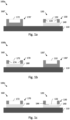
- Figs. 1a-1c show schematic views of cross sections of semiconductor devices 100a, 100b, 100c.
- the semiconductor device 100a comprises a substrate 110.
- the semiconductor device 100a comprises a radiation element 130 and detection element 170'.
- the radiation element 130 comprises a radiation layer 132 configured to radiate an electromagnetic wave.
- the detection element 170' comprises a detection layer 172 configured to detect the electromagnetic wave. That is, the radiation element 130 may radiate an electromagnetic wave to be detected by the detection element 170'.
- the radiation element 130 may be part of an emitter 120 and/or the detection element 170' may be part of a detector 160'.
- the radiation element 130 may comprise a supporting layer 134, e.g., a semiconductor substrate or a semiconductor layer.
- the radiation element 130 e.g., the radiation layer 132
- the radiation layer 132 may comprise a membrane structure or may be a membrane structure, e.g., a membrane or a diaphragm.
- the radiation element 130 may be a thermal MEMS, such as an infrared heater. That is, the radiation element 130 may be a thermally active component.
- the supporting layer 134 and the radiation layer 132 may be formed in one piece.
- the radiation layer 132 may be formed from the supporting layer 134, e.g., a semiconductor substrate, for example, by etching a portion of the supporting layer to form the radiation layer 132.
- the radiation layer 132 may be attached to the supporting layer 134.
- the supporting layer 134 may comprise multiple sub-layers (i.e., the supporting layer 134 is not formed in one piece).
- the radiation layer 132 may be formed in a sub-layer of the supporting layer 134.
- the supporting layer 134 and/or the radiation layer 132 may comprise or may be made of a semiconducting material such as silicon, silicon carbide, silicon germanium, for example.
- the supporting layer 134 and/or the radiation layer 132 may comprise or may be made of an insulating material such as silicon nitride or glass. That is, the detection element 130 may comprise or may be made of silicon nitride or glass.
- the radiation element 130 may be configured to radiate an electromagnetic wave.
- the radiation layer 132 may be configured to radiate heat or thermal radiation, e.g., infrared radiation.
- the radiation layer 132 may be configured to radiate the electromagnetic wave in an operating range, e.g., a temperature range or wavelength range, of the detection layer 172.
- the electromagnetic wave may be radiated at a first temperature range for operating the detection layer 172 for physically (i.e., according to a physical principle, e.g., the photoacoustic principle) detecting at least a first target gas between the radiation layer 132 and the detection layer 172.
- the radiation layer 132 may be configured to intermittently radiate the electromagnetic wave.
- the radiated electromagnetic wave may be absorbed, at least partially, by gas molecules which heat up accordingly. If the electromagnetic wave is no longer emitted by the radiation layer 132, no heat or thermal radiation can be absorbed anymore by the gas molecules, and they cool down again.
- This intermittent heating and cooling induces a pressure variation.
- This pressure variation may be detected by the detection layer 172 which may transduce the measured pressure variation into a corresponding measurement signal. That is, the detection layer 172 may be configured to detect the electromagnetic wave radiated by the radiation layer 132.
- the detection layer 172 may be configured to detect indirectly the electromagnetic wave radiated by the radiation layer 132.
- the detection layer 172 may be configured to detect a pressure variation induced by the electromagnetic wave.
- the detection layer 172 may be part of a thermal sensor.
- the detection layer 172 may be configured to detect directly the electromagnetic wave radiated by the radiation layer 132. That is, the detection layer 172 may be configured to determine an absorption spectrum of the electromagnetic wave, for example. In this case, the detection layer 172 may be part of a direct absorption sensor.
- the detection element 170 may comprise a supporting layer 174, e.g., a semiconductor substrate or a semiconductor layer.
- the detection element 170 e.g., the detection layer 172
- the detection layer 172 may comprise or may be a microphone structure, e.g., a MEMS microphone, a pressure sensitive transducer, a piezo transducer, a capacitive sensor, a thermal sensitive structure, a mechanical strain sensitive structure and/or a magnetic field sensitive structure.
- the detection element 170 may be a thermally sensitive component.
- the semiconductor device 100a, 100b, 100c may be used in a MEMS gas sensor, such as in a miniaturized photo acoustic spectrometer sensor or a thermally sensitive device (see Fig. 6 ).
- the supporting layer 174 and the detection layer 172 may be formed in one piece. That is, the detection layer 172 may be formed from the supporting layer 174, e.g., a semiconductor substrate, for example, by etching a portion of the supporting layer to form the detection layer 172. Alternatively, the detection layer 172 may be attached to the supporting layer 174. Optionally or alternatively, the supporting layer 174 may comprise multiple sub-layers (i.e., the supporting layer 174 is not formed in one piece). For example, the detection layer 172 may be formed in a sub-layer of the supporting layer 174.
- the supporting layer 174 and/or the detection layer 172 may comprise or may be made of a semiconducting material such as silicon, silicon carbide, silicon germanium and/or a piezoelectric material such as lithium niobate, aluminum nitride, barium titanate, for example.
- the supporting layer 174 and/or the detection layer 172 may comprise or may be made of an insulating material such as silicon nitride or glass. That is, the detection element 170 may comprise or may be made of silicon nitride or glass.
- the substrate 110 may be a printed circuit board or a lead frame, for example. Because the radiation element 130, 130' and the detection element 170, 170' may be thermally connected through the substrate 110, heat generated in the radiation element 130, 130' may affect the functionality of the detection element 170, 170'. The smaller the distance between the radiation element 130, 130'and the detection element 170, 170' become, the faster they can react to temperature changes (i.e., thermal capacity decreases and thermal modulation increases). Thermal modulation on the radiation element 130, 130' (caused by the process of radiating the electromagnetic wave) may create a modulated differential pressure.
- the modulated differential pressure may interfere with the optically generated photoacoustic signal, i.e., the induced pressure variation of the gas, and thus may negatively affect the detection element 170,170'. That is, thermal modulation on the radiation element 130, 130' (e.g., by a parasitic thermal signal) may conduct to the thermally sensitive detection element 170, 170' and may affect the sensitivity of the detection element 170, 170' due to cross-coupling. Therefore, the accuracy of the detection element 170, 170' may be decreased and/or an error of the detection element 170, 170' may be increased.
- a defined conductive thermal interface may be necessary to adjust a thermal conductivity and a thermal path in a way to demodulate parasitic thermal signals (caused by the radiation element 130, 130' radiating the electromagnetic wave) from sensor measurement signals (the electromagnetic wave measured by the detection element 170, 170').
- the conductive thermal interface may be provided by the interface layer 140, 180.
- an emitter or a detector does not comprise a separate interface layer.
- a detector 160' and an emitter 120' do not normally have an interface layer (see Figs. 1a and Figs. 1b , respectively).
- a material between the radiation element 130'/the detection element 170' and the substrate 110 is identical to a material of the radiation element 130'/the detection element 170'. Therefore, parasitic thermal signal induced by an emitter 120' can negatively affect the detector 160'.
- the conductive thermal interface i.e., the interface layer 140, 180
- the conductive thermal interface can reduce cross-coupling between radiation element 130, 130' and detection element 170, 170'.
- the interface layer 140, 180 may comprise a smaller or a larger thermal conductivity than the radiation element 130 and/or the detection element 170.
- an interface layer 140 may be only arranged between the radiation element 130 and the substrate 110.
- an interface layer 180 may be only arranged between the detection element 170 and the substrate 110 (see Fig. 1b ).
- an interface layer 140 may be arranged between the radiation element 130 and the substrate 110 and an interface layer 180 may be arranged between the detection element 170 and the substrate 110 (see Fig. 1c ).
- the interface layer 140, 180 may allow to provide a thermally isolated material stack (e.g., the emitter 120 or the detector 160) utilizing a thermally decoupling material (part of the interface layer 140, 180), e.g., an insulating material or a conductive material, with a thermal conductivity different from the thermal conductivity of the radiation element 130 and/or the detection element 170.
- the thermally decoupling material may demodulate the thermal oscillation caused by the radiation element 130 out of a frequency of the induced pressure variation to be detected by the detection element 170'. In this way, the modulated parasitic temperature oscillations of a material stack may be converted to a slow temperature drift by the thermally isolated material stack. That is, the thermally isolated material stack may be improved for a thermal path.
- the thermally isolated material stack may be combined with an arrangement as flip-chip mounting (e.g., see Figs. 1c , 3d , 4a, 4b , 5b, 5c , 6a ). In this way, cross-coupling between radiation element 130, 130' and detection 170', 170 can be reduced in a facilitated way.
- the thermally isolated material stack design may be used for the emitter 120 and/or the detector 160.
- Fig. 1c shows an example of an emitter 120 assembled using flip-chip mounting.
- the interface layer 140 may be manufactured as a "cap layer" of an intermediate semiconductor device.
- the intermediate semiconductor device may be attached to the substrate 110 using flip-chip mounting.
- the "cap layer” of the intermediate semiconductor device may become the interface layer 140.
- the radiation element 130 may be supported by the interface layer 140.
- the radiation element 130 may face the interface layer 140.
- the thermally isolated material stack comprising an interface layer 140, 180 may improve a performance of the detection element 170', 170 (due to a lower parasitic signal) and/or may allow to size-down/shrink the distance between the radiation element 130, 130' and the detection element 170', 170 due to thermal improvement possible.
- the interface layer 140, 180 may comprise or may be made of (i.e., the thermally decoupling material may comprise or may be made of) an insulating material, such as glass or silicon nitride or a conductive material such as doped silicon (if the radiation element 130'/detection element 170' comprises or is made of undoped silicon), monocrystalline silicon (if the radiation element 130'/detection element 170' comprises or is made of polycrystalline silicon) or a metal such as copper, gold, silver.
- an insulating material such as glass or silicon nitride or a conductive material such as doped silicon (if the radiation element 130'/detection element 170' comprises or is made of undoped silicon), monocrystalline silicon (if the radiation element 130'/detection element 170' comprises or is made of polycrystalline silicon) or a metal such as copper, gold, silver.
- a thickness of the interface layer 140, 180 may be at least 10 ⁇ m, or at least 30 ⁇ m, or at least 50 ⁇ m, or at least 100 ⁇ m and/or at most 1400 ⁇ m, or at most 1600 ⁇ m, or at most 1800 ⁇ m, or at most 2000 ⁇ m.
- a material of the (emitter) interface layer 140 may be different from a material of the (detector) interface layer 180, e.g., the (emitter) interface layer material may be an insulating material and the (detector) interface layer material may be a conductive material or a different insulating material.
- the (emitter) interface layer 140 may comprise a conductive material and the (detector) interface layer 180 may comprise an insulating material. In this way, parameters of the emitter 120 and the detector 160 can be adjusted independently.
- the thermal conductivity of the radiation element 130 and/or the detection element 170 may be different from the thermal conductivity of the interface layer 140, 180 by a factor of at least 5, or at least 7, or at least 9, or at least 10, or at least 12, or at least 14. In this way, the interface layer 140, 180 can thermally decouple the radiation element 130 and/or the detection element 170.
- a difference by a factor can mean that the thermal conductivity is either smaller by this factor or larger by this factor.
- the thermal conductivity of the interface layer 140, 180 may be 10 times larger or ten times smaller than the thermal conductivity of the radiation element 130 or the detection element 170.
- the radiation element 130 and/or the detection element 170 may comprise or may be made of silicon (150-170 W/(m*K)) and the interface layer 140, 180 may comprise or may be made of silicon nitride (10-50 W/(m*K)), glass (1,5 W/(m*K)) or a metal such as copper (398 W/(m*K)), gold (315 W/(m*K)), silver (429 W/(m*K)).
- the radiation element 130 and/or the detection element may comprise or may be made of glass (e.g., the supporting layer 134, 174 may comprise or may be made of glass) and the interface layer 140, 180 may be made of silicon (e.g., doped silicon, undoped silicon, monocrystalline silicon or polycrystalline silicone).
- the interface layer 140, 180 may partially thermally decouple the radiation element 130/detection element 170 from the substrate 110. In this way, a cross-coupling can be reduced and a performance of the detection element 170, 170' can be improved.
- the interface layer 140, 180 may be a conductive layer.
- the interface layer 140, 180 may have a thermal conductivity of at least 150 W/(m*K), or at least 170 W/(m*K), or at least 190 W/(m*K), or at least 200 W/(m*K) or at least 300 W/(m*K), or at least 380 W/(m*K).
- Decreasing or increasing the heat transfer between radiation element 130/detection element 170 and the substrate 110 may allow to improve a thermal decoupling of the radiation element 130 from the detection element 170, 170' and/or the detection element 170 from the radiation element 130, 130'. In this way, a cross-coupling can be reduced even further and a performance of the detection element 170, 170' can be improved.
- the interface layer 140, 180 may comprise glass or may be made of glass.
- the glass may comprise or may be made of silicon oxide such as silica quartz or phosphosilicate glass.
- the interface layer 140, 180 may act as insulating layer.
- glass may facilitate a handling of the emitter 120/detector 160, such as attachment to the substrate 110.
- an interface layer 140, 180 comprising glass may provide an improved interface between interface layer 140, 180 and substrate 110, as in comparison to an adhesive.
- the interface layer 140, 180 may comprise a surface, which could be attached to the substrate 110.
- an adhesive may not be required to attach an interface layer 140, 180, such as a glass layer or a silicon nitride layer, to a surface. In this way, an interface between the substrate 110 and the emitter 120/the detector 160 can be improved. For example, an inaccurate contact between interface layer 140 and surface due to the adhesive can be avoided.
- the interface layer 140, 180 may be directly attached to the substrate 110.
- the interface layer 140, 180 may be attached to the substrate 110 by bonding, e.g., glass to silicon anodic bonding, glass frit bonding, eutectic, transient liquid metal or metal to metal thermocompression bonding.
- bonding e.g., glass to silicon anodic bonding, glass frit bonding, eutectic, transient liquid metal or metal to metal thermocompression bonding.
- adhesive-free wafer bonding techniques such as surface-activated bonding or hydrophilic bonding, can be used to attach the interface layer 140, 180 to the substrate 110. These methods rely on surface activation or modification to create a bond without the use of adhesives. Since the interface layer 140, 180 can be attached directly to the substrate 110, an interface between the emitter 120/the detector 160 and the substrate 110 can be improved.
- the interface layer 140, 180 may be a "cap layer" of an intermediate semiconductor device.
- the radiation layer 132 may face the interface layer 140, 180. That is, the radiation layer 132 may be formed on or in a surface of the radiation element 130 facing the interface layer 140, 180.
- the interface layer 140, 180 may comprise a cavity 144. Further, the radiation layer 132 may face the cavity.
- the radiation layer 132 may be arranged above the cavity 144 to prevent a contact between interface layer 140, 180 and radiation layer 132.
- a thermally isolated material stack (comprising the interface layer 140, 180 and the radiation element 130) may be attached to the substrate 110 (e.g., using flip-chip mounting).
- the interface layer 140, 180 may be attached to the substrate 110 and the radiation element 130 may be attached to the interface layer 140, 180. That is, both the emitter 120 and the detector 160 can each be formed using flip-chip mounting or alternatively, by attaching the interface layer 140, 180 to the substrate 110 and by attaching the radiation element 130/detection element 170 to the interface layer 140, 180.
- the interface layer 140, 180 may be attached to the radiation element 130 and/or the detection element 170.
- the radiation element 130 may be an emitting layer 130.
- the emitting layer 130 may comprise the radiation layer 132. That is, the emitting layer 130 may be configured to radiate the electromagnetic wave.
- the emitting layer 130 may be formed separately from the interface layer 140.
- the emitting layer 130 may be attached to the interface layer 140.
- the emitting layer 130 may be attached to the supporting layer 134 and the supporting layer 134 may be attached to the interface layer 140.
- the emitting layer 130 may be directly attached to the interface layer 140.
- the radiation element 130 may be a thermally active component and the detection element 170 may be a thermally sensitive component.
- the radiation element 130 or the detection element 170 may be electrically connected to the substrate 110 by a coupling element.
- the radiation element 130 and the detection element 170 may be connected by multiple coupling elements to the substrate 110.
- the coupling element may be an electrical connection between the radiation element 130/the detection 170 and the substrate 110.
- the coupling element may comprise or may be a solder ball, a via, an electrically conductive adhesive and/or a wire bond.
- the semiconductor device 100a, 100b, 100c may further comprise an underfill layer arranged between the radiation element 130 or the detection element 170 and the substrate 110 (see also Figs. 4 , 5b, 5c ).
- the underfill layer may improve a stability of the emitter 120 and/or the detector 160.
- the underfill layer may increase a design flexibility of the semiconductor device 100a, 100b, 100c.
- a material of the underfill layer can be chosen depending on a thermal conductivity. That is, a thermal conductivity of the emitter 120/the detector 160 can be adjusted using the underfill layer. Thus, the thermal conductivity can be adjusted using the underfill layer during a back-end-of-line process.
- the thermal conductivity of the emitter 120/the detector 160 can be adjusted using front-end-of-line processes, e.g., bonding the interface layer 140, 170 on the substrate 110 and using back-end-of-line processes, e.g., forming the underfill layer.
- the semiconductor device 100a, 100b, 100c may further comprise a cap layer arranged above the radiation element 130 and/or the detection element 170.
- the cap layer is transparent for infrared light.
- the cap layer may cover the radiation element 130 and/or the detection element 170.
- the cap layer may not block or may not interfere with the radiated electromagnetic wave.
- the cap layer may further act to thermally decouple the radiation element 130 and/or the detection element 170.
- a thermal conductivity of the cap layer may be different from a thermal conductivity of the radiation element and/or the detection element (e.g., see Figs. 2 , 3b ).
- Fig. 1 may comprise one or more optional or additional features corresponding to one or more aspects mentioned in connection with the proposed concept or one or more examples described below (e.g., Fig. 2 - 8 ).
- Fig. 2 shows a schematic view of a cross section of another example of a semiconductor device 200.
- the semiconductor device 200 comprises a substrate 210. Further, the semiconductor device 200 comprises a radiation element 230 and detection element 270.
- the radiation element 230 comprises a radiation layer 232 configured to radiate an electromagnetic wave.
- the detection element 270 comprises a detection layer 272 configured to detect the electromagnetic wave. That is, the radiation element 230 may radiate an electromagnetic wave to be detected by the detection element 270.
- the radiation element 230 may be part of an emitter 220 and/or the detection element 270 may be part of a detector 260.
- arranging the radiation element 230 and the detection element 270 in a semiconductor device 200 may lead to cross-coupling.
- the cross-coupling can be reduced by an interface layer as described with reference to Fig. 1 .
- the cross-coupling can also be reduced by a cap layer 250, 290 .
- the semiconductor device 200 may comprise a cap layer 250, 290 arranged above the radiation element 230 and/or the detection element 270.
- a thermal conductivity of the radiation element 230 and/or the detection element 270 may be different from a thermal conductivity of the cap layer 250, 290.
- the cap layer 250, 290 may affect a heat generation and/or a heat distribution in the emitter 220 and/or the detector 260. Therefore, a heat transfer to the substrate 210 can be adjusted using the cap layer 250, 290.
- the cap layer 250, 290 may cause an increased heat transfer towards the substrate 210 or a decreased heat transferred towards the substrate 210. In this way, undesired heat generated in the emitter 210 and transferred into the substrate 210 can be at least partially thermally decoupled from the intended electromagnetic wave radiated of the radiation element 230.
- the cap layer 250, 290 may be a separate layer attached to the radiation element 230/the detection element 270.
- the above description ( Fig. 1 ) of the interface layer also applies to the cap layer 250, 290. That is, the cap layer 250, 290 can have the same properties and parameters as the interface layer.
- the cap layer 250, 290 can be combined with an interface layer. In this case, the adjustment of heat transfer can be facilitated.
- Fig. 2 shows only exemplary a cap layer 250 above the radiation element 230 and a cap layer 290 above the detection element 270.
- a cap layer 250 or a cap layer 290 may be disposed only over the radiation element 230 or only over the detection element 270, respectively.
- Fig. 2 may comprise one or more optional or additional features corresponding to one or more aspects mentioned in connection with the proposed concept or one or more examples described above (e.g., Fig. 1 ) and/or below (e.g., Fig. 3 -8 ).
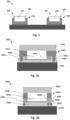
- Figs. 3a-3d show schematic views of cross sections of other examples of a part of a semiconductor device.
- Figs. 3a-3d show exemplary an emitter 320a, 320b, 320c, 320d with a three-layer stack, namely interface layer 336a, 340b, 340c, 340d, radiation element 330a, 330b, 330c, 330d comprising the supporting structure 334a, 334b, 334c, 334d and the cap layer 350a, 350b, 356c, 356d.
- the three-layer stack is an example. In other examples, the stack may comprise less layers, e.g., two layers (see Fig. 5 ) or more layers.
- the interface layer 336a, 340b, 340c, 340d and/or the radiation element 330a, 330b, 330c, 330d may comprise multiple layers.
- the substrate 310a and the interface layer 336a may comprise or may be made of silicon and may be bonded together.
- silicon to silicon bonding can be done by glass frit bonding, eutectic, transient liquid metal or metal to metal thermocompression bonding.
- Fig. 3b shows an example of an emitter 320b.
- the emitter 320b may be part of a semiconductor device according to Fig. 1 and/or Fig. 2 .
- the emitter 320b may comprise a substrate 310b, an interface layer 340b, a radiation element 330b and a cap layer 350b.
- the thermal conductivity of the interface layer 340b may be different from the thermal conductivity of the radiation element 330b.
- the thermal conductivity of the radiation element 330b may be different from the thermal conductivity of the cap layer 350b.
- the radiation element 330b may comprise a supporting layer 334b configured to support the radiation layer. Further, Fig.
- the cap layer 350b and/or the interface layer 340b may comprise or may be made of glass or a silicon nitride.
- the radiation element 330b may comprise or may be made of semiconducting material such as silicon, silicon carbide, silicon germanium and/or a piezoelectric material such as lithium niobate, aluminum nitride, barium titanate, for example.
- the interface layer 340b may be attached to the substrate 310b using bonding techniques, e.g., anodic bonding, glass frit bonding, eutectic, transient liquid metal or metal to metal thermocompression bonding.
- bonding techniques e.g., anodic bonding, glass frit bonding, eutectic, transient liquid metal or metal to metal thermocompression bonding.
- Fig. 3c shows an example of an emitter 320c.
- the emitter 320c may be part of a semiconductor device according to Fig. 1 .
- the emitter 320c may comprise a substrate 310c, an interface layer 340c, a radiation element 330c and a cap layer 356c.
- the thermal conductivity of the interface layer 340c may be different from the thermal conductivity of the radiation element 330c.
- the thermal conductivity of the radiation element 330c may be identical to the thermal conductivity of the cap layer 356c. Thus, a thermally decoupling can be achieved using the interface layer 340c.
- the radiation element 330c may comprise a supporting layer 334c configured to support the radiation layer. Further, Fig.
- the interface layer 340c may comprise or may be made of glass or a silicon nitride.
- the radiation element 330c and/or the cap layer 356c may comprise or may be made of semiconducting material such as silicon, silicon carbide, silicon germanium, for example.
- the interface layer 340c may be attached to the substrate 3 10c using an attachment layer 342c.
- the attachment layer 342c may comprise or may be made of an adhesive or an elastomer.
- Fig. 3d shows an example of an emitter 320d.
- the emitter 320d may be part of a semiconductor device according to Fig. 1 .
- the emitter 320d may comprise a substrate 310d, an interface layer 340d, a radiation element 330d and a cap layer 356d.
- the thermal conductivity of the interface layer 340d may be different from the thermal conductivity of the radiation element 330d.
- the thermal conductivity of the radiation element 330d may be identical to the thermal conductivity of the cap layer 356d. Thus, a thermally decoupling can be achieved using the interface layer 340d.
- the radiation element 330d may comprise a supporting layer 334d configured to support the radiation layer. Further, Fig.
- the 3d shows a coupling element 302d, e.g., a through substrate via such as a through glass via, configured to electrically connect the substrate 3 10d with the radiation element 330d.
- the interface layer 340d may comprise or may be made of glass or a silicon nitride.
- the radiation element 330d and/or the cap layer 356d may comprise or may be made of semiconducting material such as silicon, silicon carbide, silicon germanium, for example.
- the radiation layer 332d may face the interface layer 340d.
- the interface layer 340d may comprise a cavity 344c.
- the radiation layer 332d may face the cavity 344d. That is, a surface of the radiation element 330d on or in which the radiation element 332d is formed may face the interface layer 340d. Therefore, Fig. 3d shows an emitter 320d, which may be manufactured using flip-chip mounting.
- Figs. 3a-3d of the emitter 320a, 320b, 320c, 320d also applies to a detector.
- the emitter 320b according to Fig. 3b may comprise a through silicon via instead of a wire bond and optionally may be manufactured using flip-chip mounting or the semiconductor device 300d according to Fig. 3d may comprise a cap layer 356d comprising or made of glass or a silicon nitride.
- Fig. 1 and Fig. 2 show separated approaches for emitters and detectors for a semiconductor device, they can be combined.
- a semiconductor device may comprise an emitter according to Fig. 3d and a detector according to Fig. 3a .
- Fig. 3 may comprise one or more optional or additional features corresponding to one or more aspects mentioned in connection with the proposed concept or one or more examples described above (e.g., Fig. 1 - 2 ) and/or below (e.g., Fig. 4 - 8 ).
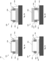
- Figs. 4a-4b show schematic views of cross sections of other examples of a part of a semiconductor device.
- Fig. 4a shows an emitter 420a.
- the emitter 420a may be part of a semiconductor device according to Fig. 1 .
- the emitter 420a may comprise a substrate 410a, an interface layer 440a, a radiation element 430a and a cap layer 456a.
- the emitter 420a may further comprise an optional underfill layer 408a.
- the underfill layer 408a may be arranged between the substrate 410a and the radiation element 430a.
- the underfill layer 408a may partially surround the interface layer 440a. That is, the interface layer 440a may be embedded in the underfill layer 408a.
- the interface layer 440a may comprise a cavity 444a.
- the radiation layer 432a of the radiation element 430a may face the cavity 444a. That is, the emitter 420a may be manufactured using flip-chip mounting.
- the emitter 420a comprises a coupling element 402a.
- the coupling element 402a may be a solder ball or a cupper pillar.
- the coupling element 402a may be partially surrounded by the underfill material 408a.
- a solder ball or a cupper pillar may be advantageously if the interface layer 440a has a smaller cross-section than the radiation element 430a.
- a thermally isolated material stack can be flip chip soldered onto the substrate 410a, e.g., a lead frame or a printed circuit board, by solder balls or cupper pillars.
- the coupling element 402b may be electrically connected with a conductive trace 409a, e.g., a solder cap arranged on top of the interface layer 440a and the underfill 408a.
- the conductive trace 409a may be electrically connected to the radiation layer 432a.
- the underfill 408a may increase a stability of the emitter 420a and/or may protect the coupling element 402a, e.g., prevent corrosion.
- the interface layer 440a may comprise or may be made of glass or silicon nitride.
- the radiation element 430a and/or the cap layer 456a may comprise or may be made of semiconducting material such as silicon, silicon carbide, silicon germanium, for example.
- Fig. 4b shows another example of an emitter 420b.
- the emitter 420b may be part of a semiconductor device according to Fig. 1 .
- the emitter 420b may comprise a substrate 410b, an interface layer 440b, a radiation element 430b and a cap layer 456b.
- the emitter 420b may further comprise an optional underfill layer 408a.
- the underfill layer 408b may be arranged between the substrate 410b and the radiation element 430b. As can be seen in Fig. 4a , the underfill layer 408b may partially surround the interface layer 440b. That is, the interface layer 440b may be embedded in the underfill layer 408b.
- the interface layer 440b may comprise a cavity 444b.
- the radiation layer 432b of the radiation element 430b may face the cavity 444b. That is, the emitter 420b may be manufactured using flip-chip mounting.
- the emitter 420a comprises a coupling element 402a.
- the cross-section of the interface layer 440b may be at least identical to the cross-section of the radiation element 430b. Therefore, the coupling element 402a may comprise a through substrate via 406b, such as a through glass via 406b, and a solder ball 404b. The solder ball 404b may be partially surrounded by the underfill material 408b.
- the through glass via 406 may have been formed, for example, through a glass "cap layer" of an intermediate semiconductor device.
- the intermediate semiconductor device can be flip chip mounted onto the substrate 410b, e.g., a lead frame or a printed circuit board, by solder balls or cupper pillars.
- the coupling element 402b may be electrically connected with a conductive trace 409b, e.g., a solder cap arranged on top of the interface layer 440b.
- the conductive trace 409b may be electrically connected to the radiation layer 432b.
- Figs. 4a-4b of the emitter 420a, 420b also applies to a detector.
- Fig. 4 may comprise one or more optional or additional features corresponding to one or more aspects mentioned in connection with the proposed concept or one or more examples described above (e.g., Fig. 1 - 3 ) and/or below (e.g., Fig. 5 - 8 ).
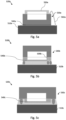
- Fig. 5a shows a coupling element 502a, e.g., a wire bond 502a, configured to electrically connect the substrate 510a with the radiation element 530a.
- the cap layer 550a may comprise or may be made of glass or a silicon nitride.
- the radiation element 530a may comprise or may be made of semiconducting material such as silicon, silicon carbide, silicon germanium, for example.
- Fig. 5 may comprise one or more optional or additional features corresponding to one or more aspects mentioned in connection with the proposed concept or one or more examples described above (e.g., Fig. 1 - 4 ) and/or below (e.g., Fig. 6 - 8 ).
- the photoacoustic sensor 600a may comprise a substrate 610a, e.g., a printed circuit board or a lead frame.
- a cover 694a may be arranged on the substrate 610a.
- the cover 694a may be configured to cover the emitter 620a and the detector 660a. Further, the cover 694a may form the measurement cavity 696a. That is, the cover 694a may be configured to reflect the electromagnetic wave radiated from the emitter 620a.
- the cover 694a may provide a housing for the emitter 620a and the detector 660a.
- the cover 694a may comprise an opening 692a configured to provide a fluid communication with a surrounding, for example, for allowing an environmental gas and/or a target gas to enter the measurement cavity 696a.
- the opening 692a may be arranged in a top wall (i.e., the wall facing the substrate 610a) of the cover 694a.
- the opening and/or another opening may be arranged in a side wall of the cover 694a.
- the semiconductor device 600a, 600b may provide a detector, e.g., a Si-microphone, packaged with wafer level bonding processes under a defined gas-sensing atmosphere, e.g., CO 2 or vacuum.
- the semiconductor device may provide a non-dispersive infrared sensor packaged with wafer level bonding processes. Typical photoacoustic sensors use silicon as bottom interface and top interface as connection to the sensing volume. Instead the semiconductor device 600a, 600b uses different materials to allow for adjustment of thermal conductivity to reduce cross-coupling.
- Fig. 6 may comprise one or more optional or additional features corresponding to one or more aspects mentioned in connection with the proposed concept or one or more examples described above (e.g., Fig. 1 - 5 ) and/or below (e.g., Fig. 7 - 8 ).
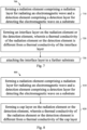
- Fig. 7 shows a block diagram of a method 700 for manufacturing a semiconductor device.
- the method 700 comprises forming 710 a radiation element comprising a radiation layer for radiating an electromagnetic wave and a detection element comprising a detection layer for detecting the electromagnetic wave on a substrate.
- the method 700 further comprises 720 forming an interface layer on the radiation element or the detection element.
- a thermal conductivity of the radiation element and/or the detection element is different from a thermal conductivity of the interface layer.
- the method 700 comprises attaching 730 the interface layer to a further substrate.
- a part of a or semiconductor device as described above, e.g., with reference to Figs. 1-6 can be formed according to method 700.
- attaching the interface layer to the further substrate may comprise a flip-chip process.
- the interface layer can be manufactured as cap layer on top of the radiation element/the detection element and can be arranged as interface layer by flip-chip mounting.
- a thermal MEMS such as an infrared heater
- a photoacoustic sensor 600a, 600b may be manufactured using wafer level bonding.
- the method 700 may further comprise forming an underfill layer with a back-end-of-line process.
- a thermal conductivity of the underfill layer is different from a thermal conductivity of the radiation element or the detection element.
- a thermal conductivity of an emitter/detector can be adjusted using a back-end-of-line process. That is, a thermal conductivity can be adjusted after front-end-of-line processing is finished, e.g., after glass to silicon bonding.
- Fig. 7 may comprise one or more optional or additional features corresponding to one or more aspects mentioned in connection with the proposed concept or one or more examples described above (e.g., Fig. 1 - 6 ) and/or below (e.g., Fig. 8 ).
- Fig. 8 shows a block diagram of a method 800 for manufacturing a semiconductor device.
- the method 800 comprises forming 810 a radiation element comprising a radiation layer for radiating an electromagnetic wave and a detection element comprising a detection layer for detecting the electromagnetic wave on a substrate.
- the method 800 further comprises forming 820 a cap layer on the radiation element or the detection element.
- a thermal conductivity of the radiation element and/or the detection element is different from a thermal conductivity of the cap layer.
- a part of a or a semiconductor device as described above, e.g., with reference to Figs. 1-6 can be formed according to method 800.
- Fig. 8 may comprise one or more optional or additional features corresponding to one or more aspects mentioned in connection with the proposed concept or one or more examples described above (e.g., Fig. 1 - 7 ).
- Examples may further be or relate to a (computer) program including a program code to execute one or more of the above methods when the program is executed on a computer, processor or other programmable hardware component.
- steps, operations or processes of different ones of the methods described above may also be executed by programmed computers, processors or other programmable hardware components.
- Examples may also cover program storage devices, such as digital data storage media, which are machine-, processor- or computer-readable and encode and/or contain machine-executable, processor-executable or computer-executable programs and instructions.
- Program storage devices may include or be digital storage devices, magnetic storage media such as magnetic disks and magnetic tapes, hard disk drives, or optically readable digital data storage media, for example.
- aspects described in relation to a device or system should also be understood as a description of the corresponding method.
- a block, device or functional aspect of the device or system may correspond to a feature, such as a method step, of the corresponding method.
- aspects described in relation to a method shall also be understood as a description of a corresponding block, a corresponding element, a property or a functional feature of a corresponding device or a corresponding system.
- An example (e.g., example 1) relates to a semiconductor device, comprising a radiation element comprising a radiation layer for radiating an electromagnetic wave and a detection element comprising a detection layer for detecting the electromagnetic wave, a substrate, and an interface layer arranged between the radiation element or the detection element and the substrate, wherein a thermal conductivity of the radiation element or the detection element is different from a thermal conductivity of the interface layer.
- Another example relates to a previous example (e.g., example 1) or to any other example, further comprising that the thermal conductivity of the radiation element or the detection element is different from the thermal conductivity of the interface layer by a factor of at least 10.
- Another example (e.g., example 4) relates to a previous example (e.g., one of the examples 1 to 3) or to any other example, further comprising that the interface layer comprises glass or is made of glass.
- Another example (e.g., example 5) relates to a previous example (e.g., one of the examples 1 to 4) or to any other example, further comprising that the interface layer is directly attached to the substrate.
- Another example (e.g., example 6) relates to a previous example (e.g., one of the examples 1 to 5) or to any other example, further comprising that the radiation element or the detection element is electrically coupled to the substrate by a coupling element.
- Another example (e.g., example 7) relates to a previous example (e.g., example 6) or to any other example, further comprising that the coupling element comprises at least one of a solder ball, a via, an electrically conductive adhesive and a wire bond.
- Another example (e.g., example 8) relates to a previous example (e.g., one of the examples 1 to 7) or to any other example, further comprising that the interface layer is directly attached to the radiation element or the detection element.
- Another example (e.g., example 9) relates to a previous example (e.g., one of the examples 1 to 8) or to any other example, further comprising an underfill layer arranged between the radiation element or the detection element and the substrate.
- Another example (e.g., example 10) relates to a previous example (e.g., example 9) or to any other example, further comprising that the underfill layer is arranged between the interface layer and the substrate.
- Another example (e.g., example 11) relates to a previous example (e.g., example 9) or to any other example, further comprising that the interface layer is at least partially embedded in the underfill layer.
- Another example relates to a previous example (e.g., example 12) or to any other example, further comprising a solder ball electrically coupling the radiation element or the detection element with the substrate, wherein the solder ball is partially embedded in the underfill layer.
- Another example relates to a previous example (e.g., example 12) or to any other example, further comprising that the solder ball extends along a lateral dimension of the interface layer.
- Another example relates to a previous example (e.g., one of the examples 1 to 13) or to any other example, further comprising that the radiation element comprises a membrane.
- Another example relates to a previous example (e.g., one of the examples 1 to 14) or to any other example, further comprising that the detection element comprises at least one of a pressure sensitive transducer, a piezo transducer, a capacitive sensor, a thermal sensitive structure, a mechanical strain sensitive structure and a magnetic field sensitive structure.
- the detection element comprises at least one of a pressure sensitive transducer, a piezo transducer, a capacitive sensor, a thermal sensitive structure, a mechanical strain sensitive structure and a magnetic field sensitive structure.
- Another example (e.g., example 16) relates to a previous example (e.g., one of the examples 1 to 15) or to any other example, further comprising a cap layer arranged above the radiation element or the detection element, the cap layer is transparent for infrared light.
- An example (e.g., example 17) relates to a semiconductor device, comprising a radiation element comprising a radiation layer for radiating an electromagnetic wave or a detection element comprising a detection layer for detecting the electromagnetic wave, a substrate, and a cap layer arranged above the radiation element or the detection element, wherein a thermal conductivity of the radiation element or the detection element is different from a thermal conductivity of the cap layer.
- An example (e.g., example 18) relates to a microelectromechanical system, MEMS, gas sensor, comprising a semiconductor device according to any one of the preceding examples.
- An example (e.g., example 19) relates to a method, comprising forming a radiation element comprising a radiation layer for radiating an electromagnetic wave and a detection element comprising a detection layer for detecting the electromagnetic wave on a substrate, forming an interface layer on the radiation element or the detection element, wherein a thermal conductivity of the radiation element or the detection element is different from a thermal conductivity of the interface layer, and attaching the interface layer to a further substrate.
- Another example relates to a previous example (e.g., example 19) or to any other example, further comprising attaching the interface layer to the further substrate comprises a flip-chip process.
- Another example (e.g., example 21) relates to a previous example (e.g., one of the examples 19 or 20) or to any other example, further comprising forming an underfill layer with a back-end-of-line process, wherein a thermal conductivity of the underfill layer is different from a thermal conductivity of the radiation element or the detection element.
- An example (e.g., example 22) relates to a method, comprising forming a radiation element comprising a radiation layer for radiating an electromagnetic wave and a detection element comprising a detection layer for detecting the electromagnetic wave on a substrate, and forming a cap layer on the radiation element or the detection element, wherein a thermal conductivity of the radiation element or the detection element is different from a thermal conductivity of the cap layer.
Landscapes
- Physics & Mathematics (AREA)
- Engineering & Computer Science (AREA)
- General Physics & Mathematics (AREA)
- Chemical & Material Sciences (AREA)
- Health & Medical Sciences (AREA)
- General Health & Medical Sciences (AREA)
- Analytical Chemistry (AREA)
- Immunology (AREA)
- Pathology (AREA)
- Biochemistry (AREA)
- Life Sciences & Earth Sciences (AREA)
- Microelectronics & Electronic Packaging (AREA)
- Manufacturing & Machinery (AREA)
- Computer Hardware Design (AREA)
- Electrochemistry (AREA)
- Chemical Kinetics & Catalysis (AREA)
- Toxicology (AREA)
- Thermal Sciences (AREA)
- Photometry And Measurement Of Optical Pulse Characteristics (AREA)
- Investigating Or Analyzing Materials By The Use Of Electric Means (AREA)
- Investigating Or Analysing Materials By Optical Means (AREA)
Abstract
Examples provide a semiconductor device. The semiconductor device comprises a radiation element and a detection element. The radiation element comprises a radiation layer for radiating an electromagnetic wave. The detection element comprises a detection layer for detecting the electromagnetic wave. Further, the semiconductor device comprises a substrate and an interface layer. The interface layer is arranged between the radiation element and/or the detection element and the substrate. A thermal conductivity of the radiation element and/or the detection element is different from a thermal conductivity of the interface layer.
Description
- Examples relate to semiconductor devices, a microelectromechanical system gas sensor and methods.
- The sensing of environmental parameters, such as noise, sound, temperature and gases gains more and more importance within mobile devices, home automatization and the automotive sector. In a sensor device, mechanical and thermal couplings play a major role for cross-coupling and readout quality, such as for microelectromechanical system (MEMS) as well as environmental sensors and others. However, cross-coupling can have a negative impact on the performance of the sensor device. Therefore, there is a demand for an improved concept to reduce cross-coupling.
- This demand may be satisfied by the subject matter of the independent claims.
- Some aspects of the present disclosure relate to a semiconductor device comprising a radiation element and a detection element. The radiation element comprises a radiation layer for radiating an electromagnetic wave. The detection element comprises a detection layer for detecting the electromagnetic wave. Further, the semiconductor device comprises a substrate and an interface layer. The interface layer is arranged between the radiation element and/or the detection element and the substrate. A thermal conductivity of the radiation element and/or the detection element is different from a thermal conductivity of the interface layer.
- Some aspects of the present disclosure relate to a semiconductor device comprising a radiation element and a detection element. The radiation element comprises a radiation layer for radiating an electromagnetic wave. The detection element comprises a detection layer for detecting the electromagnetic wave. Further, the semiconductor device comprises a substrate and a cap layer. The cap layer is arranged above the radiation element and/or the detection element. A thermal conductivity of the radiation element and/or the detection element is different from a thermal conductivity of the cap layer.
- Some aspects of the present disclosure relate to a MEMS gas sensor comprising a semiconductor device as described above.
- Some aspects of the present disclosure relate to a method comprising forming a radiation element comprising a radiation layer for radiating an electromagnetic wave and a detection element comprising a detection layer for detecting the electromagnetic wave on a substrate. The method further comprises forming an interface layer on the radiation element or the detection element. A thermal conductivity of the radiation element and/or the detection element is different from a thermal conductivity of the interface layer. Further, the method comprises attaching the interface layer to a further substrate.
- Some aspects of the present disclosure relate to a method comprising forming a radiation element comprising a radiation layer for radiating an electromagnetic wave and a detection element comprising a detection layer for detecting the electromagnetic wave on a substrate. The method further comprises forming a cap layer on the radiation element or the detection element. A thermal conductivity of the radiation element and/or the detection element is different from a thermal conductivity of the cap layer.
- Some examples of apparatuses and/or methods will be described in the following by way of example only, and with reference to the accompanying figures, in which
-
Figs. 1a-1c show schematic views of cross sections of semiconductor devices; -
Fig. 2 shows a schematic view of a cross section of another example of a semiconductor device; -
Figs. 3a-3d show schematic views of cross sections of other examples of a part of a semiconductor device; -
Figs. 4a-4b show schematic views of cross sections of other examples of a part of a semiconductor device; -
Figs. 5a-5c show schematic views of cross sections of other examples of a part of a semiconductor device; -
Figs. 6a-6b show schematic views of cross sections of examples of a semiconductor device; -
Fig. 7 shows a block diagram of a method for manufacturing a semiconductor device; and -
Fig. 8 shows a block diagram of a method for manufacturing a semiconductor device. - Some examples are now described in more detail with reference to the enclosed figures. However, other possible examples are not limited to the features of these embodiments described in detail. Other examples may include modifications of the features as well as equivalents and alternatives to the features. Furthermore, the terminology used herein to describe certain examples should not be restrictive of further possible examples.
- Throughout the description of the figures same or similar reference numerals refer to same or similar elements and/or features, which may be identical or implemented in a modified form while providing the same or a similar function. The thickness of lines, layers and/or areas in the figures may also be exaggerated for clarification.
- When two elements A and B are combined using an "or", this is to be understood as disclosing all possible combinations, i.e., only A, only B as well as A and B, unless expressly defined otherwise in the individual case. As an alternative wording for the same combinations, "at least one of A and B" or "A and/or B" may be used. This applies equivalently to combinations of more than two elements.
- If a singular form, such as "a", "an" and "the" is used and the use of only a single element is not defined as mandatory either explicitly or implicitly, further examples may also use several elements to implement the same function. If a function is described below as implemented using multiple elements, further examples may implement the same function using a single element or a single processing entity. It is further understood that the terms "include", "including", "comprise" and/or "comprising", when used, describe the presence of the specified features, integers, steps, operations, processes, elements, components and/or a group thereof, but do not exclude the presence or addition of one or more other features, integers, steps, operations, processes, elements, components and/or a group thereof.
-
Figs. 1a-1c show schematic views of cross sections ofsemiconductor devices Fig. 1a thesemiconductor device 100a comprises asubstrate 110. Further, thesemiconductor device 100a comprises aradiation element 130 and detection element 170'. Theradiation element 130 comprises aradiation layer 132 configured to radiate an electromagnetic wave. The detection element 170' comprises adetection layer 172 configured to detect the electromagnetic wave. That is, theradiation element 130 may radiate an electromagnetic wave to be detected by the detection element 170'. For example, theradiation element 130 may be part of anemitter 120 and/or the detection element 170' may be part of a detector 160'. - The
radiation element 130 may comprise a supportinglayer 134, e.g., a semiconductor substrate or a semiconductor layer. Theradiation element 130, e.g., theradiation layer 132, may be supported by the supportinglayer 134. For example, theradiation layer 132 may comprise a membrane structure or may be a membrane structure, e.g., a membrane or a diaphragm. For example, theradiation element 130 may be a thermal MEMS, such as an infrared heater. That is, theradiation element 130 may be a thermally active component. The supportinglayer 134 and theradiation layer 132 may be formed in one piece. That is, theradiation layer 132 may be formed from the supportinglayer 134, e.g., a semiconductor substrate, for example, by etching a portion of the supporting layer to form theradiation layer 132. Alternatively, theradiation layer 132 may be attached to the supportinglayer 134. Optionally or alternatively, the supportinglayer 134 may comprise multiple sub-layers (i.e., the supportinglayer 134 is not formed in one piece). For example, theradiation layer 132 may be formed in a sub-layer of the supportinglayer 134. The supportinglayer 134 and/or theradiation layer 132 may comprise or may be made of a semiconducting material such as silicon, silicon carbide, silicon germanium, for example. Alternatively, the supportinglayer 134 and/or theradiation layer 132 may comprise or may be made of an insulating material such as silicon nitride or glass. That is, thedetection element 130 may comprise or may be made of silicon nitride or glass. - The
radiation element 130, e.g., theradiation layer 132, may be configured to radiate an electromagnetic wave. For example, theradiation layer 132 may be configured to radiate heat or thermal radiation, e.g., infrared radiation. Theradiation layer 132 may be configured to radiate the electromagnetic wave in an operating range, e.g., a temperature range or wavelength range, of thedetection layer 172. For example, the electromagnetic wave may be radiated at a first temperature range for operating thedetection layer 172 for physically (i.e., according to a physical principle, e.g., the photoacoustic principle) detecting at least a first target gas between theradiation layer 132 and thedetection layer 172. - For example, the
radiation layer 132 may be configured to intermittently radiate the electromagnetic wave. The radiated electromagnetic wave may be absorbed, at least partially, by gas molecules which heat up accordingly. If the electromagnetic wave is no longer emitted by theradiation layer 132, no heat or thermal radiation can be absorbed anymore by the gas molecules, and they cool down again. This intermittent heating and cooling induces a pressure variation. This pressure variation may be detected by thedetection layer 172 which may transduce the measured pressure variation into a corresponding measurement signal. That is, thedetection layer 172 may be configured to detect the electromagnetic wave radiated by theradiation layer 132. Thus, thedetection layer 172 may be configured to detect indirectly the electromagnetic wave radiated by theradiation layer 132. That is, thedetection layer 172 may be configured to detect a pressure variation induced by the electromagnetic wave. In this case, thedetection layer 172 may be part of a thermal sensor. Optionally or alternatively, thedetection layer 172 may be configured to detect directly the electromagnetic wave radiated by theradiation layer 132. That is, thedetection layer 172 may be configured to determine an absorption spectrum of the electromagnetic wave, for example. In this case, thedetection layer 172 may be part of a direct absorption sensor. - As can be seen in
Fig. 1b , thedetection element 170 may comprise a supporting layer 174, e.g., a semiconductor substrate or a semiconductor layer. Thedetection element 170, e.g., thedetection layer 172, may be supported by the supporting layer 174. For example, thedetection layer 172 may comprise or may be a microphone structure, e.g., a MEMS microphone, a pressure sensitive transducer, a piezo transducer, a capacitive sensor, a thermal sensitive structure, a mechanical strain sensitive structure and/or a magnetic field sensitive structure. For example, thedetection element 170 may be a thermally sensitive component. Thus, thesemiconductor device Fig. 6 ). - The supporting layer 174 and the
detection layer 172 may be formed in one piece. That is, thedetection layer 172 may be formed from the supporting layer 174, e.g., a semiconductor substrate, for example, by etching a portion of the supporting layer to form thedetection layer 172. Alternatively, thedetection layer 172 may be attached to the supporting layer 174. Optionally or alternatively, the supporting layer 174 may comprise multiple sub-layers (i.e., the supporting layer 174 is not formed in one piece). For example, thedetection layer 172 may be formed in a sub-layer of the supporting layer 174. The supporting layer 174 and/or thedetection layer 172 may comprise or may be made of a semiconducting material such as silicon, silicon carbide, silicon germanium and/or a piezoelectric material such as lithium niobate, aluminum nitride, barium titanate, for example. Alternatively, the supporting layer 174 and/or thedetection layer 172 may comprise or may be made of an insulating material such as silicon nitride or glass. That is, thedetection element 170 may comprise or may be made of silicon nitride or glass. - The
substrate 110 may be a printed circuit board or a lead frame, for example. Because theradiation element 130, 130' and thedetection element 170, 170' may be thermally connected through thesubstrate 110, heat generated in theradiation element 130, 130' may affect the functionality of thedetection element 170, 170'. The smaller the distance between theradiation element 130, 130'and thedetection element 170, 170' become, the faster they can react to temperature changes (i.e., thermal capacity decreases and thermal modulation increases). Thermal modulation on theradiation element 130, 130' (caused by the process of radiating the electromagnetic wave) may create a modulated differential pressure. The modulated differential pressure may interfere with the optically generated photoacoustic signal, i.e., the induced pressure variation of the gas, and thus may negatively affect the detection element 170,170'. That is, thermal modulation on theradiation element 130, 130' (e.g., by a parasitic thermal signal) may conduct to the thermallysensitive detection element 170, 170' and may affect the sensitivity of thedetection element 170, 170' due to cross-coupling. Therefore, the accuracy of thedetection element 170, 170' may be decreased and/or an error of thedetection element 170, 170' may be increased. - To reduce cross-coupling the
radiation element 130 and/or thedetection element 170 may be at least partially thermally decoupled. This can be achieved by use of an interface layer 140 (seeFigs. 1a and 1c ) and/or an interface layer 180 (seeFigs. 1b and 1c ) having a different thermal conductivity from theradiation element 130 or thedetection element 170, respectively. For example, a thermal or mechanical interconnection for thermal stress sensitive devices as MEMS microphones, sensors or sensitive components may comprise thesemiconductor device interface layer - It is a finding of the inventors, that a defined conductive thermal interface may be necessary to adjust a thermal conductivity and a thermal path in a way to demodulate parasitic thermal signals (caused by the
radiation element 130, 130' radiating the electromagnetic wave) from sensor measurement signals (the electromagnetic wave measured by thedetection element 170, 170'). The conductive thermal interface may be provided by theinterface layer Figs. 1a and Figs. 1b , respectively). A material between the radiation element 130'/the detection element 170' and thesubstrate 110 is identical to a material of the radiation element 130'/the detection element 170'. Therefore, parasitic thermal signal induced by an emitter 120' can negatively affect the detector 160'. - The conductive thermal interface, i.e., the
interface layer radiation element 130, 130' anddetection element 170, 170'. For example, theinterface layer radiation element 130 and/or thedetection element 170. - As can be seen in
Fig. 1a , aninterface layer 140 may be only arranged between theradiation element 130 and thesubstrate 110. Optionally or alternatively, aninterface layer 180 may be only arranged between thedetection element 170 and the substrate 110 (seeFig. 1b ). Optionally or alternatively, aninterface layer 140 may be arranged between theradiation element 130 and thesubstrate 110 and aninterface layer 180 may be arranged between thedetection element 170 and the substrate 110 (seeFig. 1c ). - The
interface layer emitter 120 or the detector 160) utilizing a thermally decoupling material (part of theinterface layer 140, 180), e.g., an insulating material or a conductive material, with a thermal conductivity different from the thermal conductivity of theradiation element 130 and/or thedetection element 170. The thermally decoupling material may demodulate the thermal oscillation caused by theradiation element 130 out of a frequency of the induced pressure variation to be detected by the detection element 170'. In this way, the modulated parasitic temperature oscillations of a material stack may be converted to a slow temperature drift by the thermally isolated material stack. That is, the thermally isolated material stack may be improved for a thermal path. Optionally the thermally isolated material stack may be combined with an arrangement as flip-chip mounting (e.g., seeFigs. 1c ,3d ,4a, 4b ,5b, 5c ,6a ). In this way, cross-coupling betweenradiation element 130, 130' anddetection 170', 170 can be reduced in a facilitated way. The thermally isolated material stack design may be used for theemitter 120 and/or thedetector 160. - For example,
Fig. 1c shows an example of anemitter 120 assembled using flip-chip mounting. In this case, theinterface layer 140 may be manufactured as a "cap layer" of an intermediate semiconductor device. The intermediate semiconductor device may be attached to thesubstrate 110 using flip-chip mounting. In this way, the "cap layer" of the intermediate semiconductor device may become theinterface layer 140. Thus, theradiation element 130 may be supported by theinterface layer 140. Theradiation element 130 may face theinterface layer 140. - The thermally isolated material stack comprising an
interface layer radiation element 130, 130' and thedetection element 170', 170 due to thermal improvement possible. - For example, the
interface layer interface layer interface layer 140 may be different from a material of the (detector)interface layer 180, e.g., the (emitter) interface layer material may be an insulating material and the (detector) interface layer material may be a conductive material or a different insulating material. For example, the (emitter)interface layer 140 may comprise a conductive material and the (detector)interface layer 180 may comprise an insulating material. In this way, parameters of theemitter 120 and thedetector 160 can be adjusted independently. - In an example, the thermal conductivity of the
radiation element 130 and/or thedetection element 170 may be different from the thermal conductivity of theinterface layer interface layer radiation element 130 and/or thedetection element 170. A difference by a factor can mean that the thermal conductivity is either smaller by this factor or larger by this factor. For example, the thermal conductivity of theinterface layer radiation element 130 or thedetection element 170. For example, theradiation element 130 and/or thedetection element 170 may comprise or may be made of silicon (150-170 W/(m*K)) and theinterface layer radiation element 130 and/or the detection element may comprise or may be made of glass (e.g., the supportinglayer 134, 174 may comprise or may be made of glass) and theinterface layer interface layer radiation element 130/detection element 170 from thesubstrate 110. In this way, a cross-coupling can be reduced and a performance of thedetection element 170, 170' can be improved. - To improve thermal decoupling the
interface layer interface layer interface interface layer radiation element 130/thedetection element 170 and thesubstrate 110 may be strongly attenuated. Alternatively, theinterface layer interface layer radiation element 130/detection element 170 and thesubstrate 110 may allow to improve a thermal decoupling of theradiation element 130 from thedetection element 170, 170' and/or thedetection element 170 from theradiation element 130, 130'. In this way, a cross-coupling can be reduced even further and a performance of thedetection element 170, 170' can be improved. - In an example, the
interface layer interface layer emitter 120/detector 160, such as attachment to thesubstrate 110. In addition, aninterface layer interface layer substrate 110, as in comparison to an adhesive. Theinterface layer substrate 110. For example, an adhesive may not be required to attach aninterface layer substrate 110 and theemitter 120/thedetector 160 can be improved. For example, an inaccurate contact betweeninterface layer 140 and surface due to the adhesive can be avoided. - In an example, the
interface layer substrate 110. For example, theinterface layer substrate 110 by bonding, e.g., glass to silicon anodic bonding, glass frit bonding, eutectic, transient liquid metal or metal to metal thermocompression bonding. For example, adhesive-free wafer bonding techniques, such as surface-activated bonding or hydrophilic bonding, can be used to attach theinterface layer substrate 110. These methods rely on surface activation or modification to create a bond without the use of adhesives. Since theinterface layer substrate 110, an interface between theemitter 120/thedetector 160 and thesubstrate 110 can be improved. - As described above with reference to
Fig. 1c , theinterface layer radiation layer 132 may face theinterface layer radiation layer 132 may be formed on or in a surface of theradiation element 130 facing theinterface layer interface layer cavity 144. Further, theradiation layer 132 may face the cavity. For example, theradiation layer 132 may be arranged above thecavity 144 to prevent a contact betweeninterface layer radiation layer 132. In this case, a thermally isolated material stack (comprising theinterface layer interface layer substrate 110 and theradiation element 130 may be attached to theinterface layer emitter 120 and thedetector 160 can each be formed using flip-chip mounting or alternatively, by attaching theinterface layer substrate 110 and by attaching theradiation element 130/detection element 170 to theinterface layer - In an example, the
interface layer radiation element 130 and/or thedetection element 170. For example, theradiation element 130 may be an emittinglayer 130. The emittinglayer 130 may comprise theradiation layer 132. That is, the emittinglayer 130 may be configured to radiate the electromagnetic wave. The emittinglayer 130 may be formed separately from theinterface layer 140. Thus, the emittinglayer 130 may be attached to theinterface layer 140. For example, the emittinglayer 130 may be attached to the supportinglayer 134 and the supportinglayer 134 may be attached to theinterface layer 140. Alternatively, the emittinglayer 130 may be directly attached to theinterface layer 140. - For example, the
detection element 170 may be a measuring layer. Themeasuring layer 170 may comprise thedetection layer 172. That is, themeasuring layer 170 may be configured to measure the electromagnetic wave. Themeasuring layer 170 may be formed separately from theinterface layer 180. Thus, themeasuring layer 170 may be attached to theinterface layer 180. For example, themeasuring layer 170 may be attached to the supporting layer 174 and the supporting layer 174 may be attached to theinterface layer 180. Alternatively, themeasuring layer 170 may be directly attached to theinterface layer 180. - As described above, the
radiation element 130 may be a thermally active component and thedetection element 170 may be a thermally sensitive component. Thus, in an example, theradiation element 130 or thedetection element 170 may be electrically connected to thesubstrate 110 by a coupling element. For example, theradiation element 130 and thedetection element 170 may be connected by multiple coupling elements to thesubstrate 110. The coupling element may be an electrical connection between theradiation element 130/thedetection 170 and thesubstrate 110. In an example, the coupling element may comprise or may be a solder ball, a via, an electrically conductive adhesive and/or a wire bond. - In an example, the
semiconductor device radiation element 130 or thedetection element 170 and the substrate 110 (see alsoFigs. 4 ,5b, 5c ). The underfill layer may improve a stability of theemitter 120 and/or thedetector 160. Further, the underfill layer may increase a design flexibility of thesemiconductor device emitter 120/thedetector 160 can be adjusted using the underfill layer. Thus, the thermal conductivity can be adjusted using the underfill layer during a back-end-of-line process. In this way, the thermal conductivity of theemitter 120/thedetector 160 can be adjusted using front-end-of-line processes, e.g., bonding theinterface layer substrate 110 and using back-end-of-line processes, e.g., forming the underfill layer. - In an example, the underfill layer may be arranged between the
interface layer substrate 110. In an example, theinterface layer semiconductor device interface layer - In an example, the
semiconductor device radiation element 130 and/or thedetection element 170. The cap layer is transparent for infrared light. The cap layer may cover theradiation element 130 and/or thedetection element 170. The cap layer may not block or may not interfere with the radiated electromagnetic wave. The cap layer may further act to thermally decouple theradiation element 130 and/or thedetection element 170. For example, a thermal conductivity of the cap layer may be different from a thermal conductivity of the radiation element and/or the detection element (e.g., seeFigs. 2 ,3b ). - More details and aspects are mentioned in connection with the examples described below. The example shown in
Fig. 1 may comprise one or more optional or additional features corresponding to one or more aspects mentioned in connection with the proposed concept or one or more examples described below (e.g.,Fig. 2 - 8 ). -
Fig. 2 shows a schematic view of a cross section of another example of asemiconductor device 200. Thesemiconductor device 200 comprises a substrate 210. Further, thesemiconductor device 200 comprises aradiation element 230 anddetection element 270. Theradiation element 230 comprises aradiation layer 232 configured to radiate an electromagnetic wave. Thedetection element 270 comprises adetection layer 272 configured to detect the electromagnetic wave. That is, theradiation element 230 may radiate an electromagnetic wave to be detected by thedetection element 270. For example, theradiation element 230 may be part of anemitter 220 and/or thedetection element 270 may be part of adetector 260. - As described with reference to
Fig. 1 , arranging theradiation element 230 and thedetection element 270 in asemiconductor device 200 may lead to cross-coupling. The cross-coupling can be reduced by an interface layer as described with reference toFig. 1 . Optionally or alternatively, the cross-coupling can also be reduced by acap layer - Thus, the
semiconductor device 200 may comprise acap layer radiation element 230 and/or thedetection element 270. A thermal conductivity of theradiation element 230 and/or thedetection element 270 may be different from a thermal conductivity of thecap layer cap layer emitter 220 and/or thedetector 260. Therefore, a heat transfer to the substrate 210 can be adjusted using thecap layer cap layer radiation element 230. - The
cap layer radiation element 230/thedetection element 270. The above description (Fig. 1 ) of the interface layer also applies to thecap layer cap layer - Optionally, the
cap layer -
Fig. 2 shows only exemplary acap layer 250 above theradiation element 230 and acap layer 290 above thedetection element 270. In other examples, acap layer 250 or acap layer 290 may be disposed only over theradiation element 230 or only over thedetection element 270, respectively. - More details and aspects are mentioned in connection with the examples described above and/or below. The example shown in
Fig. 2 may comprise one or more optional or additional features corresponding to one or more aspects mentioned in connection with the proposed concept or one or more examples described above (e.g.,Fig. 1 ) and/or below (e.g.,Fig. 3 -8 ). -
Figs. 3a-3d show schematic views of cross sections of other examples of a part of a semiconductor device.Figs. 3a-3d show exemplary anemitter interface layer radiation element structure cap layer Fig. 5 ) or more layers. Optionally, theinterface layer radiation element -
Fig. 3a shows an example of anemitter 320a. Theemitter 320a may be part of a semiconductor device according toFig. 2 . Theemitter 320a may comprise asubstrate 310a, aninterface layer 336a, aradiation element 330a and acap layer 350a. The thermal conductivity of theinterface layer 336a may be identical to the thermal conductivity of theradiation element 330a. The thermal conductivity of theradiation element 330a may be different from the thermal conductivity of thecap layer 350a. Thus, a thermally decoupling can be achieved using thecap layer 350a. Theradiation element 330a may comprise a supportinglayer 334a configured to support the radiation layer. Further,Fig. 3a shows acoupling element 302a, e.g., awire bond 302a, configured to electrically connect thesubstrate 310a with theradiation element 330a. For example, thecap layer 350a may comprise or may be made of glass or a silicon nitride. Theradiation element 330a and/or theinterface layer 336a may comprise or may be made of semiconducting material such as silicon, silicon carbide, silicon germanium, for example. - The
substrate 310a and theinterface layer 336a may comprise or may be made of silicon and may be bonded together. For example, silicon to silicon bonding can be done by glass frit bonding, eutectic, transient liquid metal or metal to metal thermocompression bonding. -
Fig. 3b shows an example of anemitter 320b. Theemitter 320b may be part of a semiconductor device according toFig. 1 and/orFig. 2 . Theemitter 320b may comprise asubstrate 310b, aninterface layer 340b, aradiation element 330b and acap layer 350b. The thermal conductivity of theinterface layer 340b may be different from the thermal conductivity of theradiation element 330b. The thermal conductivity of theradiation element 330b may be different from the thermal conductivity of thecap layer 350b. Thus, a thermally decoupling can be achieved using thecap layer 350b and theinterface layer 340b. Theradiation element 330b may comprise a supportinglayer 334b configured to support the radiation layer. Further,Fig. 3b shows acoupling element 302b, e.g., awire bond 302b, configured to electrically connect thesubstrate 310b with theradiation element 330b. For example, thecap layer 350b and/or theinterface layer 340b may comprise or may be made of glass or a silicon nitride. Theradiation element 330b may comprise or may be made of semiconducting material such as silicon, silicon carbide, silicon germanium and/or a piezoelectric material such as lithium niobate, aluminum nitride, barium titanate, for example. - The
interface layer 340b may be attached to thesubstrate 310b using bonding techniques, e.g., anodic bonding, glass frit bonding, eutectic, transient liquid metal or metal to metal thermocompression bonding. -
Fig. 3c shows an example of anemitter 320c. Theemitter 320c may be part of a semiconductor device according toFig. 1 . Theemitter 320c may comprise asubstrate 310c, aninterface layer 340c, aradiation element 330c and acap layer 356c. The thermal conductivity of theinterface layer 340c may be different from the thermal conductivity of theradiation element 330c. The thermal conductivity of theradiation element 330c may be identical to the thermal conductivity of thecap layer 356c. Thus, a thermally decoupling can be achieved using theinterface layer 340c. Theradiation element 330c may comprise a supportinglayer 334c configured to support the radiation layer. Further,Fig. 3c shows acoupling element 302c, e.g., awire bond 302c, configured to electrically connect thesubstrate 310c with theradiation element 330c. For example, theinterface layer 340c may comprise or may be made of glass or a silicon nitride. Theradiation element 330c and/or thecap layer 356c may comprise or may be made of semiconducting material such as silicon, silicon carbide, silicon germanium, for example. - In contrast to
Fig. 3b theinterface layer 340c may be attached to the substrate 3 10c using anattachment layer 342c. For example, theattachment layer 342c may comprise or may be made of an adhesive or an elastomer. -
Fig. 3d shows an example of anemitter 320d. Theemitter 320d may be part of a semiconductor device according toFig. 1 . Theemitter 320d may comprise asubstrate 310d, aninterface layer 340d, aradiation element 330d and acap layer 356d. The thermal conductivity of theinterface layer 340d may be different from the thermal conductivity of theradiation element 330d. The thermal conductivity of theradiation element 330d may be identical to the thermal conductivity of thecap layer 356d. Thus, a thermally decoupling can be achieved using theinterface layer 340d. Theradiation element 330d may comprise a supportinglayer 334d configured to support the radiation layer. Further,Fig. 3d shows acoupling element 302d, e.g., a through substrate via such as a through glass via, configured to electrically connect the substrate 3 10d with theradiation element 330d. For example, theinterface layer 340d may comprise or may be made of glass or a silicon nitride. Theradiation element 330d and/or thecap layer 356d may comprise or may be made of semiconducting material such as silicon, silicon carbide, silicon germanium, for example. - As can be seen in
Fig. 3d , theradiation layer 332d may face theinterface layer 340d. Theinterface layer 340d may comprise a cavity 344c. Theradiation layer 332d may face thecavity 344d. That is, a surface of theradiation element 330d on or in which theradiation element 332d is formed may face theinterface layer 340d. Therefore,Fig. 3d shows anemitter 320d, which may be manufactured using flip-chip mounting. - The description of
Figs. 3a-3d of theemitter - Even if different features are shown in the individual
Figs. 3a-3d , they can be combined with each other. For example, theemitter 320b according toFig. 3b may comprise a through silicon via instead of a wire bond and optionally may be manufactured using flip-chip mounting or the semiconductor device 300d according toFig. 3d may comprise acap layer 356d comprising or made of glass or a silicon nitride. - Even if
Fig. 1 andFig. 2 show separated approaches for emitters and detectors for a semiconductor device, they can be combined. For example, a semiconductor device may comprise an emitter according toFig. 3d and a detector according toFig. 3a . - More details and aspects are mentioned in connection with the examples described above and/or below. The example shown in
Fig. 3 may comprise one or more optional or additional features corresponding to one or more aspects mentioned in connection with the proposed concept or one or more examples described above (e.g.,Fig. 1 - 2 ) and/or below (e.g.,Fig. 4 - 8 ). -
Figs. 4a-4b show schematic views of cross sections of other examples of a part of a semiconductor device.Fig. 4a shows anemitter 420a. Theemitter 420a may be part of a semiconductor device according toFig. 1 . Theemitter 420a may comprise asubstrate 410a, aninterface layer 440a, aradiation element 430a and acap layer 456a. Theemitter 420a may further comprise anoptional underfill layer 408a. Theunderfill layer 408a may be arranged between thesubstrate 410a and theradiation element 430a. As can be seen inFig. 4a , theunderfill layer 408a may partially surround theinterface layer 440a. That is, theinterface layer 440a may be embedded in theunderfill layer 408a. - The
interface layer 440a may comprise acavity 444a. Theradiation layer 432a of theradiation element 430a may face thecavity 444a. That is, theemitter 420a may be manufactured using flip-chip mounting. - Further, the
emitter 420a comprises acoupling element 402a. Thecoupling element 402a may be a solder ball or a cupper pillar. Thecoupling element 402a may be partially surrounded by theunderfill material 408a. A solder ball or a cupper pillar may be advantageously if theinterface layer 440a has a smaller cross-section than theradiation element 430a. For example, a thermally isolated material stack can be flip chip soldered onto thesubstrate 410a, e.g., a lead frame or a printed circuit board, by solder balls or cupper pillars. Thecoupling element 402b may be electrically connected with aconductive trace 409a, e.g., a solder cap arranged on top of theinterface layer 440a and theunderfill 408a. Theconductive trace 409a may be electrically connected to the radiation layer 432a.Theunderfill 408a may increase a stability of theemitter 420a and/or may protect thecoupling element 402a, e.g., prevent corrosion. - The
interface layer 440a may comprise or may be made of glass or silicon nitride. Theradiation element 430a and/or thecap layer 456a may comprise or may be made of semiconducting material such as silicon, silicon carbide, silicon germanium, for example. -
Fig. 4b shows another example of anemitter 420b. Theemitter 420b may be part of a semiconductor device according toFig. 1 . Theemitter 420b may comprise asubstrate 410b, aninterface layer 440b, aradiation element 430b and acap layer 456b. Theemitter 420b may further comprise anoptional underfill layer 408a. Theunderfill layer 408b may be arranged between thesubstrate 410b and theradiation element 430b. As can be seen inFig. 4a , theunderfill layer 408b may partially surround theinterface layer 440b. That is, theinterface layer 440b may be embedded in theunderfill layer 408b. - The
interface layer 440b may comprise acavity 444b. Theradiation layer 432b of theradiation element 430b may face thecavity 444b. That is, theemitter 420b may be manufactured using flip-chip mounting. - Further, the
emitter 420a comprises acoupling element 402a. In contrast toFig. 4b , the cross-section of theinterface layer 440b may be at least identical to the cross-section of theradiation element 430b. Therefore, thecoupling element 402a may comprise a through substrate via 406b, such as a through glass via 406b, and asolder ball 404b. Thesolder ball 404b may be partially surrounded by theunderfill material 408b. - The through glass via 406 may have been formed, for example, through a glass "cap layer" of an intermediate semiconductor device. The intermediate semiconductor device can be flip chip mounted onto the
substrate 410b, e.g., a lead frame or a printed circuit board, by solder balls or cupper pillars. Thecoupling element 402b may be electrically connected with aconductive trace 409b, e.g., a solder cap arranged on top of theinterface layer 440b. Theconductive trace 409b may be electrically connected to theradiation layer 432b. - The
interface layer 440b may comprise or may be made of glass or silicon nitride. Theradiation element 430b and/or thecap layer 456b may comprise or may be made of semiconducting material such as silicon, silicon carbide, silicon germanium, for example. - The description of
Figs. 4a-4b of theemitter - More details and aspects are mentioned in connection with the examples described above and/or below. The example shown in
Fig. 4 may comprise one or more optional or additional features corresponding to one or more aspects mentioned in connection with the proposed concept or one or more examples described above (e.g.,Fig. 1 - 3 ) and/or below (e.g.,Fig. 5 - 8 ). -
Figs. 5a-5c show schematic views of cross sections of other examples of a part of a semiconductor device.Figs. 5a-5c show exemplary anemitter interface layer radiation element -
Fig. 5a shows an emitter comparable toFig. 3a . Theemitter 520a may be part of a semiconductor device according toFig. 2 . The semiconductor device may comprise asubstrate 510a, aradiation element 530a and acap layer 550a. In contrast toFig. 3a , theemitter 520a does not comprise a separated interface layer. Theradiation element 530a may comprise the radiation layer and may be attached to the substrate 5 10a. For example, anattachment layer 542a may be used to attach theradiation element 530a to thesubstrate 510a. Attaching theradiation element 530a to thesubstrate 510a may facilitate a manufacturing process of a semiconductor device. - Further,
Fig. 5a shows acoupling element 502a, e.g., awire bond 502a, configured to electrically connect thesubstrate 510a with theradiation element 530a. For example, thecap layer 550a may comprise or may be made of glass or a silicon nitride. Theradiation element 530a may comprise or may be made of semiconducting material such as silicon, silicon carbide, silicon germanium, for example. -
Fig. 5b shows an emitter comparable toFig. 4b . Theemitter 520b may be part of a semiconductor device according toFig. 1 . Theemitter 520b may comprise a substrate 5 10b, aninterface layer 540b and aradiation element 530b. In contrast toFig. 4b , theemitter 520b does not comprise a separated cap layer. Theradiation element 530b may comprise the cap layer and may be attached to theinterface layer 540b. -
Fig. 5c shows anemitter 520c comparable toFig. 4a . Theemitter 520c may be part of a semiconductor device according toFig. 1 . Theemitter 520c may comprise asubstrate 510c, aninterface layer 540c and aradiation element 530c. In contrast toFig. 4a , theemitter 520c does not comprise a separated cap layer. Theradiation element 530c may comprise the cap layer and may be attached to theinterface layer 540b. - The description of
Figs. 5a-5c of theemitter - More details and aspects are mentioned in connection with the examples described above and/or below. The example shown in
Fig. 5 may comprise one or more optional or additional features corresponding to one or more aspects mentioned in connection with the proposed concept or one or more examples described above (e.g.,Fig. 1 - 4 ) and/or below (e.g.,Fig. 6 - 8 ). -
Figs. 6a-6b show schematic views of cross sections of examples of asemiconductor device photoacoustic sensor MEMS gas sensor photoacoustic sensor - The
photoacoustic sensor 600a shown inFig. 6a may comprise anemitter 620a according toFig. 3d and adetector 660a according toFig. 3d . The interface layer may comprise a thermally decoupling material, e.g., an insulating material, with a thermal conductivity lower than the thermal conductivity of the radiation element and the detection element. In this way, a cross-coupling betweenemitter 620a anddetector 660a can be reduced. As indicated by the arrows a heat transfer from theemitter 620a to the substrate may be less than a heat transfer from the substrate to thedetector 660a. Thus, thephotoacoustic sensor 600a may have a low thermal conduction. - Furthermore, the
photoacoustic sensor 600a may comprise asubstrate 610a, e.g., a printed circuit board or a lead frame. Acover 694a may be arranged on thesubstrate 610a. Thecover 694a may be configured to cover theemitter 620a and thedetector 660a. Further, thecover 694a may form themeasurement cavity 696a. That is, thecover 694a may be configured to reflect the electromagnetic wave radiated from theemitter 620a. Thecover 694a may provide a housing for theemitter 620a and thedetector 660a. Thecover 694a may comprise anopening 692a configured to provide a fluid communication with a surrounding, for example, for allowing an environmental gas and/or a target gas to enter themeasurement cavity 696a. For example, theopening 692a may be arranged in a top wall (i.e., the wall facing thesubstrate 610a) of thecover 694a. Optionally or alternatively, the opening and/or another opening may be arranged in a side wall of thecover 694a. - The
photoacoustic sensor 600a may further comprise acontroller 698a, for example an integrated circuit, e.g., an ASIC (Application Specific Integrated Circuit). Thecontroller 698a may be arranged inside or outside themeasurement cavity 696a formed by thecover 694a. Thus, it is depicted in dashed lines inFigure 6a . Thecontroller 698a may receive the measurement signal from thedetector 660a and may process the measurement signal so as to identify the at least one target gas according to the photoacoustic principle. - The
MEMS gas sensor 600b shown inFig. 6b may comprise anemitter 620b according toFig. 3a and adetector 660b according toFig. 3a . The cap layer may comprise a thermally decoupling material, e.g., an insulating material, with a thermal conductivity lower than the thermal conductivity of the radiation element and the detection element. In this way, a cross-coupling betweenemitter 620a anddetector 660a can be reduced. As indicated by the arrows a heat transfer from theemitter 620a to thedetector 660a via the substrate may be increased by the cap layer. Thus, theMEMS gas sensor 600b may have a high thermal conduction. - Furthermore, the
photoacoustic sensor 600b may comprise asubstrate 610a, acover 694b, ameasurement cavity 696b, anopening 692b and acontroller 698b as described with reference toFig. 6a . - The
photoacoustic sensor MEMS gas sensor MEMS gas sensor MEMS gas sensor MEMS gas sensor - The
semiconductor device semiconductor device - More details and aspects are mentioned in connection with the examples described above and/or below. The example shown in
Fig. 6 may comprise one or more optional or additional features corresponding to one or more aspects mentioned in connection with the proposed concept or one or more examples described above (e.g.,Fig. 1 - 5 ) and/or below (e.g.,Fig. 7 - 8 ). -
Fig. 7 shows a block diagram of amethod 700 for manufacturing a semiconductor device. Themethod 700 comprises forming 710 a radiation element comprising a radiation layer for radiating an electromagnetic wave and a detection element comprising a detection layer for detecting the electromagnetic wave on a substrate. Themethod 700 further comprises 720 forming an interface layer on the radiation element or the detection element. A thermal conductivity of the radiation element and/or the detection element is different from a thermal conductivity of the interface layer. Further, themethod 700 comprises attaching 730 the interface layer to a further substrate. A part of a or semiconductor device as described above, e.g., with reference toFigs. 1-6 can be formed according tomethod 700. - In an example, attaching the interface layer to the further substrate may comprise a flip-chip process. In this way, the interface layer can be manufactured as cap layer on top of the radiation element/the detection element and can be arranged as interface layer by flip-chip mounting. For example, a thermal MEMS, such as an infrared heater, may be encapsulated by wafer bonding using a cap wafer of glass or low thermal conductive material. For example, a
photoacoustic sensor - In an example, the
method 700 may further comprise forming an underfill layer with a back-end-of-line process. A thermal conductivity of the underfill layer is different from a thermal conductivity of the radiation element or the detection element. In this way, a thermal conductivity of an emitter/detector can be adjusted using a back-end-of-line process. That is, a thermal conductivity can be adjusted after front-end-of-line processing is finished, e.g., after glass to silicon bonding. - More details and aspects are mentioned in connection with the examples described above and/or below. The example shown in
Fig. 7 may comprise one or more optional or additional features corresponding to one or more aspects mentioned in connection with the proposed concept or one or more examples described above (e.g.,Fig. 1 - 6 ) and/or below (e.g.,Fig. 8 ). -
Fig. 8 shows a block diagram of amethod 800 for manufacturing a semiconductor device. Themethod 800 comprises forming 810 a radiation element comprising a radiation layer for radiating an electromagnetic wave and a detection element comprising a detection layer for detecting the electromagnetic wave on a substrate. Themethod 800 further comprises forming 820 a cap layer on the radiation element or the detection element. A thermal conductivity of the radiation element and/or the detection element is different from a thermal conductivity of the cap layer. A part of a or a semiconductor device as described above, e.g., with reference toFigs. 1-6 can be formed according tomethod 800. - More details and aspects are mentioned in connection with the examples described above. The example shown in
Fig. 8 may comprise one or more optional or additional features corresponding to one or more aspects mentioned in connection with the proposed concept or one or more examples described above (e.g.,Fig. 1 - 7 ). - The aspects and features described in relation to a particular one of the previous examples may also be combined with one or more of the further examples to replace an identical or similar feature of that further example or to additionally introduce the features into the further example.
- Examples may further be or relate to a (computer) program including a program code to execute one or more of the above methods when the program is executed on a computer, processor or other programmable hardware component. Thus, steps, operations or processes of different ones of the methods described above may also be executed by programmed computers, processors or other programmable hardware components. Examples may also cover program storage devices, such as digital data storage media, which are machine-, processor- or computer-readable and encode and/or contain machine-executable, processor-executable or computer-executable programs and instructions. Program storage devices may include or be digital storage devices, magnetic storage media such as magnetic disks and magnetic tapes, hard disk drives, or optically readable digital data storage media, for example. Other examples may also include computers, processors, control units, (field) programmable logic arrays ((F)PLAs), (field) programmable gate arrays ((F)PGAs), graphics processor units (GPU), application-specific integrated circuits (ASICs), integrated circuits (ICs) or system-on-a-chip (SoCs) systems programmed to execute the steps of the methods described above.
- It is further understood that the disclosure of several steps, processes, operations or functions disclosed in the description or claims shall not be construed to imply that these operations are necessarily dependent on the order described, unless explicitly stated in the individual case or necessary for technical reasons. Therefore, the previous description does not limit the execution of several steps or functions to a certain order. Furthermore, in further examples, a single step, function, process or operation may include and/or be broken up into several sub-steps, - functions, -processes or -operations.
- If some aspects have been described in relation to a device or system, these aspects should also be understood as a description of the corresponding method. For example, a block, device or functional aspect of the device or system may correspond to a feature, such as a method step, of the corresponding method. Accordingly, aspects described in relation to a method shall also be understood as a description of a corresponding block, a corresponding element, a property or a functional feature of a corresponding device or a corresponding system.
- In the following, some examples of the proposed concept are presented:
An example (e.g., example 1) relates to a semiconductor device, comprising a radiation element comprising a radiation layer for radiating an electromagnetic wave and a detection element comprising a detection layer for detecting the electromagnetic wave, a substrate, and an interface layer arranged between the radiation element or the detection element and the substrate, wherein a thermal conductivity of the radiation element or the detection element is different from a thermal conductivity of the interface layer. - Another example (e.g., example 2) relates to a previous example (e.g., example 1) or to any other example, further comprising that the thermal conductivity of the radiation element or the detection element is different from the thermal conductivity of the interface layer by a factor of at least 10.
- Another example (e.g., example 3) relates to a previous example (e.g., one of the examples 1 or 2) or to any other example, further comprising that the interface layer has a thermal conductivity of less than 2 W/(m*K).
- Another example (e.g., example 4) relates to a previous example (e.g., one of the examples 1 to 3) or to any other example, further comprising that the interface layer comprises glass or is made of glass.
- Another example (e.g., example 5) relates to a previous example (e.g., one of the examples 1 to 4) or to any other example, further comprising that the interface layer is directly attached to the substrate.
- Another example (e.g., example 6) relates to a previous example (e.g., one of the examples 1 to 5) or to any other example, further comprising that the radiation element or the detection element is electrically coupled to the substrate by a coupling element.
- Another example (e.g., example 7) relates to a previous example (e.g., example 6) or to any other example, further comprising that the coupling element comprises at least one of a solder ball, a via, an electrically conductive adhesive and a wire bond.
- Another example (e.g., example 8) relates to a previous example (e.g., one of the examples 1 to 7) or to any other example, further comprising that the interface layer is directly attached to the radiation element or the detection element.
- Another example (e.g., example 9) relates to a previous example (e.g., one of the examples 1 to 8) or to any other example, further comprising an underfill layer arranged between the radiation element or the detection element and the substrate.
- Another example (e.g., example 10) relates to a previous example (e.g., example 9) or to any other example, further comprising that the underfill layer is arranged between the interface layer and the substrate.
- Another example (e.g., example 11) relates to a previous example (e.g., example 9) or to any other example, further comprising that the interface layer is at least partially embedded in the underfill layer.
- Another example (e.g., example 13) relates to a previous example (e.g., example 12) or to any other example, further comprising a solder ball electrically coupling the radiation element or the detection element with the substrate, wherein the solder ball is partially embedded in the underfill layer.
- Another example (e.g., example 13) relates to a previous example (e.g., example 12) or to any other example, further comprising that the solder ball extends along a lateral dimension of the interface layer.
- Another example (e.g., example 14) relates to a previous example (e.g., one of the examples 1 to 13) or to any other example, further comprising that the radiation element comprises a membrane.
- Another example (e.g., example 15) relates to a previous example (e.g., one of the examples 1 to 14) or to any other example, further comprising that the detection element comprises at least one of a pressure sensitive transducer, a piezo transducer, a capacitive sensor, a thermal sensitive structure, a mechanical strain sensitive structure and a magnetic field sensitive structure.
- Another example (e.g., example 16) relates to a previous example (e.g., one of the examples 1 to 15) or to any other example, further comprising a cap layer arranged above the radiation element or the detection element, the cap layer is transparent for infrared light.
- An example (e.g., example 17) relates to a semiconductor device, comprising a radiation element comprising a radiation layer for radiating an electromagnetic wave or a detection element comprising a detection layer for detecting the electromagnetic wave, a substrate, and a cap layer arranged above the radiation element or the detection element, wherein a thermal conductivity of the radiation element or the detection element is different from a thermal conductivity of the cap layer.
- An example (e.g., example 18) relates to a microelectromechanical system, MEMS, gas sensor, comprising a semiconductor device according to any one of the preceding examples.
- An example (e.g., example 19) relates to a method, comprising forming a radiation element comprising a radiation layer for radiating an electromagnetic wave and a detection element comprising a detection layer for detecting the electromagnetic wave on a substrate, forming an interface layer on the radiation element or the detection element, wherein a thermal conductivity of the radiation element or the detection element is different from a thermal conductivity of the interface layer, and attaching the interface layer to a further substrate.
- Another example (e.g., example 20) relates to a previous example (e.g., example 19) or to any other example, further comprising attaching the interface layer to the further substrate comprises a flip-chip process.
- Another example (e.g., example 21) relates to a previous example (e.g., one of the examples 19 or 20) or to any other example, further comprising forming an underfill layer with a back-end-of-line process, wherein a thermal conductivity of the underfill layer is different from a thermal conductivity of the radiation element or the detection element.
- An example (e.g., example 22) relates to a method, comprising forming a radiation element comprising a radiation layer for radiating an electromagnetic wave and a detection element comprising a detection layer for detecting the electromagnetic wave on a substrate, and forming a cap layer on the radiation element or the detection element, wherein a thermal conductivity of the radiation element or the detection element is different from a thermal conductivity of the cap layer.
- The following claims are hereby incorporated in the detailed description, wherein each claim may stand on its own as a separate example. It should also be noted that although in the claims a dependent claim refers to a particular combination with one or more other claims, other examples may also include a combination of the dependent claim with the subject matter of any other dependent or independent claim. Such combinations are hereby explicitly proposed, unless it is stated in the individual case that a particular combination is not intended. Furthermore, features of a claim should also be included for any other independent claim, even if that claim is not directly defined as dependent on that other independent claim.
Claims (15)
- A semiconductor device (100a; 100b; 100c), comprising:a radiation element (130; 130') comprising a radiation layer (132) for radiating an electromagnetic wave and a detection element (170; 170') comprising a detection layer for detecting the electromagnetic wave;a substrate (110); andan interface layer (140; 180) arranged between the radiation element (130) or the detection element (170) and the substrate (110), wherein a thermal conductivity of the radiation element (130) or the detection element (170) is different from a thermal conductivity of the interface layer (140; 180).
- The semiconductor device (100a; 100b; 100c) according to claim 1, wherein
the thermal conductivity of the radiation element (130) or the detection element (170) is different from the thermal conductivity of the interface layer (140; 180) by a factor of at least 10. - The semiconductor device (100a; 100b; 100c) according to any one of the preceding claims, wherein
the interface layer (140; 180) has a thermal conductivity of less than 2 W/(m*K). - The semiconductor device (100a; 100b; 100c) according to any one of the preceding claims, wherein
the interface layer (140; 180) comprises glass or is made of glass. - The semiconductor device (100a; 100b; 100c) according to any one of the preceding claims, wherein
the interface layer (140; 180) is directly attached to the substrate (110). - The semiconductor device (100a; 100b; 100c) according to any one of the preceding claims, whereinthe interface layer comprises a cavity (144) and whereinthe radiation layer (132) faces the cavity (144).
- The semiconductor device (100a; 100b; 100c) according to any one of the preceding claims, wherein
the radiation element (130) or the detection element (170) is electrically coupled to the substrate (110) by a coupling element (302a; 302b; 302c; 302d). - The semiconductor device (100a; 100b; 100c) according to claim 7, wherein
the coupling element (302a; 302b; 302c; 302d) comprises at least one of a solder ball, a via, an electrically conductive adhesive and a wire bond. - The semiconductor device (100a; 100b; 100c) according to any one of the preceding claims, wherein
the interface layer (140; 180) is directly attached to the radiation element (130) or the detection element (170). - The semiconductor device (100a; 100b; 100c) according to any one of the preceding claims, further comprising
an underfill layer (408a; 408b) arranged between the radiation element (130) or the detection element (170) and the substrate (110). - The semiconductor device according to any one of the preceding claims, further comprising
a cap layer (350a; 350b; 356c; 356d) arranged above the radiation element (130) or the detection element (170), the cap layer (350a; 350b; 356c; 356d) is transparent for infrared light. - A semiconductor device, comprising:a radiation element (230) comprising a radiation layer (232) for radiating an electromagnetic wave or a detection element (270) comprising a detection layer (272) for detecting the electromagnetic wave;a substrate (210); anda cap layer (250, 290) arranged above the radiation element (230) or the detection element (270), wherein a thermal conductivity of the radiation element (230) or the detection element (270) is different from a thermal conductivity of the cap layer (250; 290).
- A microelectromechanical system, MEMS, gas sensor, comprising:
a semiconductor device according to any one of the preceding claims. - A method, comprising:forming a radiation element comprising a radiation layer for radiating an electromagnetic wave and a detection element comprising a detection layer for detecting the electromagnetic wave on a substrate;forming an interface layer on the radiation element or the detection element, wherein a thermal conductivity of the radiation element or the detection element is different from a thermal conductivity of the interface layer; andattaching the interface layer to a further substrate.
- A method, comprising:forming a radiation element comprising a radiation layer for radiating an electromagnetic wave and a detection element comprising a detection layer for detecting the electromagnetic wave on a substrate; andforming a cap layer on the radiation element or the detection element, wherein a thermal conductivity of the radiation element or the detection element is different from a thermal conductivity of the cap layer.
Priority Applications (3)
| Application Number | Priority Date | Filing Date | Title |
|---|---|---|---|
| EP23199747.9A EP4530606A1 (en) | 2023-09-26 | 2023-09-26 | Semiconductor devices, microelectromechanical system gas sensor, methods |
| US18/830,121 US20250102422A1 (en) | 2023-09-26 | 2024-09-10 | Semiconductor devices, microelectromechanical system gas sensor, methods |
| CN202411331860.3A CN119706728A (en) | 2023-09-26 | 2024-09-24 | Semiconductor device, MEMS gas sensor, and method |
Applications Claiming Priority (1)
| Application Number | Priority Date | Filing Date | Title |
|---|---|---|---|
| EP23199747.9A EP4530606A1 (en) | 2023-09-26 | 2023-09-26 | Semiconductor devices, microelectromechanical system gas sensor, methods |
Publications (1)
| Publication Number | Publication Date |
|---|---|
| EP4530606A1 true EP4530606A1 (en) | 2025-04-02 |
Family
ID=88204277
Family Applications (1)
| Application Number | Title | Priority Date | Filing Date |
|---|---|---|---|
| EP23199747.9A Pending EP4530606A1 (en) | 2023-09-26 | 2023-09-26 | Semiconductor devices, microelectromechanical system gas sensor, methods |
Country Status (3)
| Country | Link |
|---|---|
| US (1) | US20250102422A1 (en) |
| EP (1) | EP4530606A1 (en) |
| CN (1) | CN119706728A (en) |
Citations (3)
| Publication number | Priority date | Publication date | Assignee | Title |
|---|---|---|---|---|
| EP3996473A1 (en) * | 2020-11-05 | 2022-05-11 | AT & S Austria Technologie & Systemtechnik Aktiengesellschaft | Component carrier with electronic components and thermally conductive blocks on both sides |
| US20220381753A1 (en) * | 2021-06-01 | 2022-12-01 | Infineon Technologies Ag | Sensor and method for detecting guided thermal radiation |
| EP4191232A1 (en) * | 2019-08-22 | 2023-06-07 | Infineon Technologies AG | Detector cell for a photoacoustic gas sensor and photoacoustic gas sensor |
-
2023
- 2023-09-26 EP EP23199747.9A patent/EP4530606A1/en active Pending
-
2024
- 2024-09-10 US US18/830,121 patent/US20250102422A1/en active Pending
- 2024-09-24 CN CN202411331860.3A patent/CN119706728A/en active Pending
Patent Citations (3)
| Publication number | Priority date | Publication date | Assignee | Title |
|---|---|---|---|---|
| EP4191232A1 (en) * | 2019-08-22 | 2023-06-07 | Infineon Technologies AG | Detector cell for a photoacoustic gas sensor and photoacoustic gas sensor |
| EP3996473A1 (en) * | 2020-11-05 | 2022-05-11 | AT & S Austria Technologie & Systemtechnik Aktiengesellschaft | Component carrier with electronic components and thermally conductive blocks on both sides |
| US20220381753A1 (en) * | 2021-06-01 | 2022-12-01 | Infineon Technologies Ag | Sensor and method for detecting guided thermal radiation |
Also Published As
| Publication number | Publication date |
|---|---|
| CN119706728A (en) | 2025-03-28 |
| US20250102422A1 (en) | 2025-03-27 |
Similar Documents
| Publication | Publication Date | Title |
|---|---|---|
| CN101389940B (en) | Pressure sensor with silicon frit bonded cap | |
| US7997142B2 (en) | Low pressure sensor device with high accuracy and high sensitivity | |
| CN102257372B (en) | Pressure measuring device | |
| CN102105769B (en) | Media isolated differential pressure sensor with cap | |
| CN102749159B (en) | There is the sensor component sealing structure | |
| KR100372340B1 (en) | Pressure Sensor and Method of Manufacturing the Same | |
| KR101199904B1 (en) | Infrared sensor | |
| CN107110729B (en) | Pressure measuring device | |
| US20220228974A1 (en) | Detector Cell for a Photoacoustic Gas Sensor and Photoacoustic Gas Sensor | |
| CN107152983B (en) | Pressure sensor | |
| US20080164413A1 (en) | Infrared Sensor | |
| JPS5855732A (en) | Electrostatic capacity type pressure sensor | |
| US3968466A (en) | Pressure transducer | |
| KR20110066187A (en) | Infrared sensor | |
| JPH07103837A (en) | Physical quantity detection sensor | |
| US11780727B2 (en) | Low-stress packaging structure for MEMS acceleration sensor chip | |
| CN115541071B (en) | Bipolar transistor MEMS pressure sensor and preparation method thereof | |
| JP2011203226A (en) | Infrared sensor module | |
| US20250102422A1 (en) | Semiconductor devices, microelectromechanical system gas sensor, methods | |
| JP2004163148A (en) | Semiconductor pressure sensor | |
| JP2001174324A (en) | Infrared detector and infrared detector | |
| JP2012207986A (en) | Pressure sensor | |
| JP2008032451A (en) | Capacitance change pressure sensor | |
| JP2010204112A (en) | Sensor and method for manufacturing the same | |
| JPS61272623A (en) | Electrostatic capacity type pressure sensor |
Legal Events
| Date | Code | Title | Description |
|---|---|---|---|
| PUAI | Public reference made under article 153(3) epc to a published international application that has entered the european phase |
Free format text: ORIGINAL CODE: 0009012 |
|
| STAA | Information on the status of an ep patent application or granted ep patent |
Free format text: STATUS: THE APPLICATION HAS BEEN PUBLISHED |
|
| AK | Designated contracting states |
Kind code of ref document: A1 Designated state(s): AL AT BE BG CH CY CZ DE DK EE ES FI FR GB GR HR HU IE IS IT LI LT LU LV MC ME MK MT NL NO PL PT RO RS SE SI SK SM TR |
|
| STAA | Information on the status of an ep patent application or granted ep patent |
Free format text: STATUS: REQUEST FOR EXAMINATION WAS MADE |
|
| 17P | Request for examination filed |
Effective date: 20251001 |